

Preliminary
5
4
5
4
RT9177
Ultra-Low-Noise 200mA LDO Regulator
General Description
The RT9177 is a 200mA low dropout and low noise
micro-power regulator suitable for portable RF
applications. The output voltage accuracy within
±2% and range from 2.4V to 3.2V in 100mV
increments could be selected. It is designed for
using very low ESR output capacitor. Its output
remains stable even in using 1µF ceramic as its
output capacitor.
Using an internal PMOS as the pass device cause
that don’t need extra GND current in heavy load and
dropout conditions. In shutdown mode, nearly zero
operation current cause the IC is suitable for
battery-power devices. Other features including
current limiting, over temperature protection and
adding a capacitor in bypass pin to improve its noise
performance are functional.
Ordering Information
RT9177-
Package type
B
: SOT-25 Type I
BR : SOT-25 Type II
Operating temperature range
C: Commercial standard
Output voltage
24 : 2.4V
25 : 2.5V
:
:
31 : 3.1V
32 : 3.2V
Features
z
Ultra-Low-Noise(150nV/
z
1µµµµF Ceramic C
Low Dropout Voltage(220mV @ 200mA)
z
Low Operation Current - 80µµµµA Typical
z
Shutdown Function
z
Low Temperature Coefficient
z
Current and Thermal Limiting
z
Custom Voltage Available
z
SOT-25 Package
z
OUT
Stable
) for RF Application
Hz
Applications
z Cellular Telephones
z Laptop, Notebook, and Palmtop Computers
z Battery-powered Equipment
z Hand-held Equipment
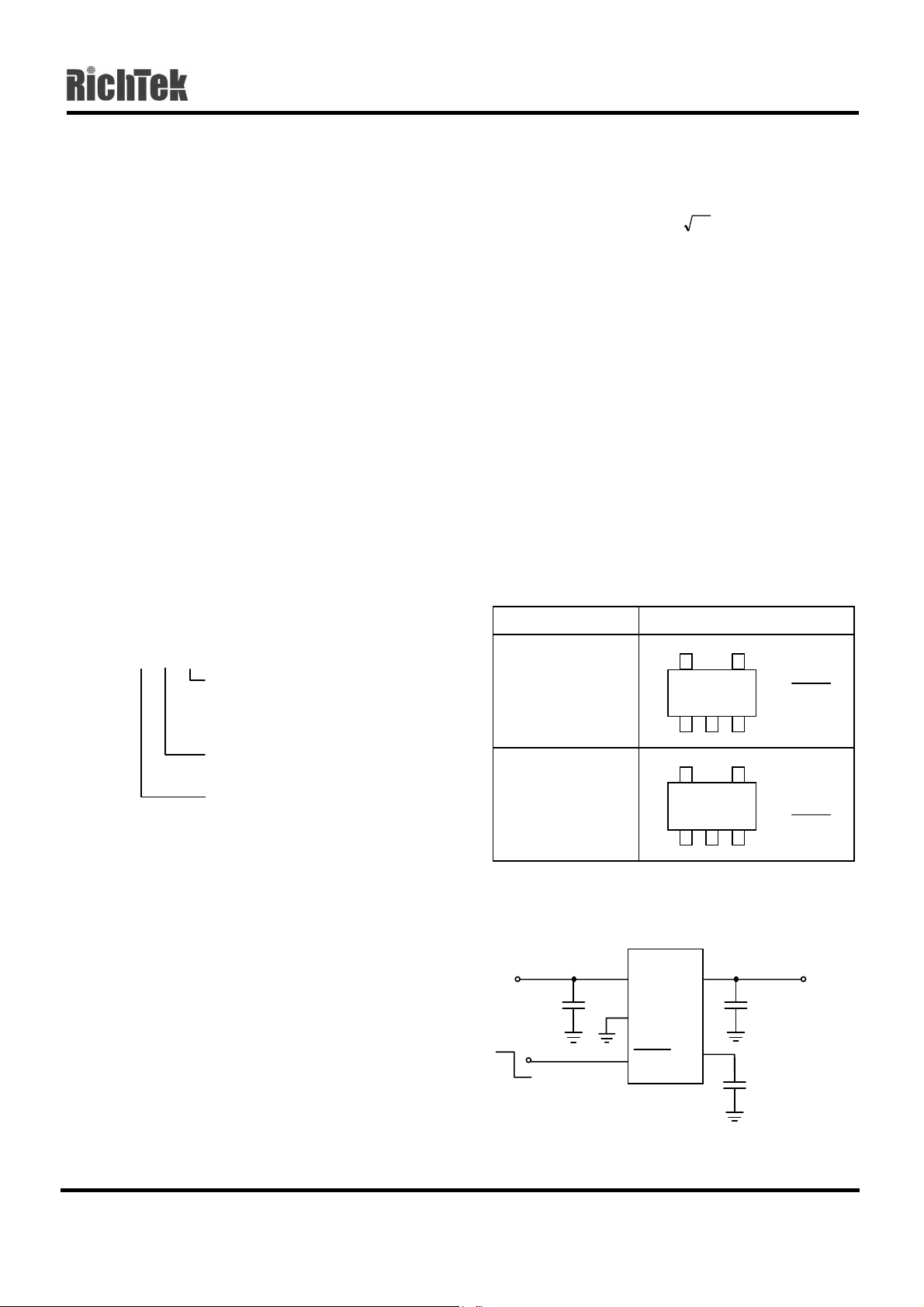
Pin Configurations
Part Number Pin Configurations
3
3
1. IN
2. GND
3. SHDN
4. BP
5. OUT
1. OUT
2. GND
3. IN
4. SHDN
5. BP
RT9177-CB
(Plastic SOT-25)
RT9177-CBR
(Plastic SOT-25)
TOP VIEW
21
TOP VIEW
21
Typical Application Circuit
RT917 7
V
IN
C
IN
1µF
ON
OFF
DS9177-00 Feb. 2001 www.richtek-ic.com.tw
IN
GND
SHDN
OUT
C
OUT
1µF
C
BP
10nF
V
OU T
1
RT9177
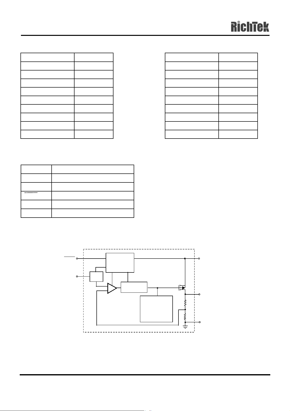
Marking Infromation
Preliminary
Part Number Marking
RT9177-24CB H9
RT9177-25CB HA
RT9177-26CB HB
RT9177-27CB HC
RT9177-28CB HD
RT9177-29CB HE
RT9177-30CB HF
RT9177-31CB HG
RT9177-32CB HH
Pin Description
Pin Name Pin Function
IN IC Power Pin
GND IC GND
SHDN Active Low Shutdown Input
Part Number Marking
RT9177-24CBR P9
RT9177-25CBR PA
RT9177-26CBR PB
RT9177-27CBR PC
RT9177-28CBR PD
RT9177-29CBR PE
RT9177-30CBR PF
RT9177-31CBR PG
RT9177-32CBR PH
BP Reference Noise Bypass
OUT Regulator Output
Function Block Diagram
SHDN
BP
VREF
Shutdown
Logic Control
+
_
Error Amp
and
MOS Driver
IN
OUT
Current-Limit
and
Thermal
Protection
GND
www.richtek-ic.com.tw DS9177-00 Feb. 2001
2
Absolute Maximum Ratings
Preliminary
RT9177
Input Voltage V
z
Power Dissipation
z
IN
7V
SOT-25 0.25W
Operating Junction Temperature Range −40°C to 125°C
z
Storage Temperature Range −65°C to 150°C
z
Thermal Resistance
z
R
θJA
Lead Temperature
z
250°C/W
(Soldering 5 sec.) 260°C
Electrical Characteristics
(V
= 5.0V, C
IN
Input Voltage
Output Voltage Accuracy
Maximum Output Current
Current Limit
GND Pin Current
Dropout Voltage
(V
(Nominal)≥3.0V Version)
OUT
Line Regulation
Load Regulation
SHDN Input High Threshold
SHDN Input Low Threshold
SHDN Bias Current
Shutdown Supply Current
Thermal Shutdown Temperature
Output Noise
Ripple Rejection PSRR
Notes: Dropout voltage definition: V
= 1µF, C
IN
OUT
= 1µF, T
= 25°C, unless otherwise specified)
A
Parameter Symbol Test Conditions Min Typ Max Units
V
IN
∆V
OUTIL
I
MAX
I
LIMIT
= 1mA
R
LOAD
= 1 Ohm
2.5 -- 6 V
-2 -- +2 %
200 -- -- mA
-- 300 -- mA
No Load -- 80 150
I
(Note)
G
V
DROP
∆V
LINEVIN
∆V
LOADIOUT
V
IH
V
IL
I
SD
I
GSD
T
SD
e
no
- V
IN
OUT
I
= 200mA
OUT
I
= 1mA
OUT
I
= 50mA
OUT
I
= 200mA
OUT
= (V
OUT
= 0mA to 200mA
VIN = 3V to 5.5V
VIN = 3V to 5.5V
V
= 0V
OUT
CBP = 10nF, C
F = 100Hz, C
when V
is 50 mV below the value of V
OUT
+0.15) to 6V, I
= 10µF
OUT
= 10nF, C
BP
OUT
OUT
= 1mA
= 10µF
-- 90 150
-- 1.1 5
-- 55 100
-- 220 300
-0.2
-- +0.2 %/V
-- 0.01 0.04 %/mA
1.0 -- -- V
-- -- 0.4 V
-- -- 100 nA
-- 0.01 1
-- 150 --
-- 150 --
nV/
-- 68 --
OUT
at V
IN
= V
OUT
+ 0.5V
µA
mV
µA
°C
Hz
dB
DS9177-00 Feb. 2001 www.richtek-ic.com.tw
3
RT9177
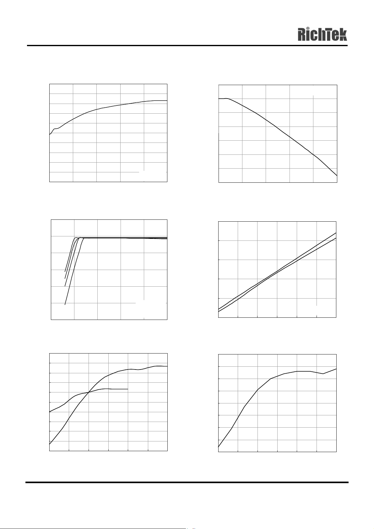
Typical Operating Characteristics
Preliminary
75
GND Current vs. Load
74
73
72
71
70
(uA)
G
I
69
68
67
66
65
0 50 100 150 200 250
I
(mA)
OUT
V
vs. V
3.10
3.00
2.90
(V)
2.80
20mA
OUT
V
50mA
2.70
100mA
2.60
2.50
200mA
2.5 3.0 3.5 4.0 4.5 5.0
OUT
VIN (V)
IN
TA = 25°C
V
OUT
T
A
= 3V
= 25°C
Output Voltage Variation vs. Load
0.2
0.0
-0.2
-0.4
(%)
OUT
-0.6
V
∆
-0.8
-1.0
-1.2
0 50 100 150 200 250
I
OUT
(mA)
Dropout Voltage vs. Output Current
250
200
150
100
Dropout Voltage (mV)
50
0
20 50 80 110 140 170 200
Output Current (mA)
TA = 25°C
80 C
25 C
V
= 3V
°
°
Output Voltage Variation vs. Temperature
0.4
0.3
0.2
0.1
0.0
(%)
-0.1
OUT
-0.2
V
∆
-0.3
-0.4
-0.5
-0.6
-40 -10 20 50 80 110 140
Temperature ( C)
No Load
200mA
°
72
71
70
69
68
(uA)
G
I
67
66
65
64
GND Current vs. Tem perature
-40 -10 20 50 80 110 140
Temperature ( C)
°
www.richtek-ic.com.tw DS9177-00 Feb. 2001
4

Preliminary
PSRR
(dB)
5
1
5-25-15-50
0
0
0
0
0
0
0-75-50-25
5
RT9177
-20
-30
-40
-50
-60
-70
PSRR (dB)
-80
-90
-100
10 100 1K 10K 100K 1M
10mA
100mA
V
OUT
T
= 25°C
A
C
BP
= 3V
= 470pF
Frequency (Hz)
Noise Signal & Spectrum Distribution
PSRR
0246810
50
150
40
50
Time (mS)
-50
30
Noise Signal (uV)
CIN = 1uF TAN
C
= 4.7uF TAN
OUT
= 10nF
C
BP
Load = 10mA
Sampling Rate = 250KHz
20
10
≈
0
-10
-20
-30
-40
-50
-60
-70
-80
-90
10 100 1K 10K 100K 1M
10mA
100mA
V
T
C
OUT
A
BP
= 3V
= 25°C
= 10nF
Frequency (Hz)
Noise Signal & Spectrum Distribution
PSRR
0246810
50
150
40
50
Time (mS)
15
50
-50
-
-
-
30
Noise Signal (uV)
≈
20
10
CIN = 1uF TAN
C
= 4.7uF TAN
OUT
CBP = 10nF
Load = 100mA
Sampling Rate = 250KHz
0
Noise Level (uV)
0 25 50 75 100 125
Frequency (KHz)
Noise Signal & Spectrum Distribution
0246810
100
250
0
80
Time (mS)
-250
60
Noise Signal (uV)
≈
40
20
0
Noise Level (uV)
0 25 50 75 100 125
CIN = 1uF TAN
= 4.7uF TAN
C
OUT
CBP = 470nF
Load = 10mA
Sampling Rate = 250KHz
Frequency (KHz)
-
25
0
-25
-50
-75
-10
0
Noise Level (uV)
0 25 50 75 100 125
Frequency (KHz)
Noise Signal & Spectrum Distribution
0246810
100
250
80
0
Time (mS)
-250
60
Noise Signal (uV)
≈
40
20
0
Noise Level (uV)
0255075100125
Frequency (KHz)
CIN = 1uF TAN
C
= 4.7uF TAN
OUT
CBP = 470nF
Load = 100mA
Sampling Rate = 250KHz
-3
2
0
-1
DS9177-00 Feb. 2001 www.richtek-ic.com.tw
5

RT9177
Preliminary
Load Transitne Response
from 1m A to 100m A
4
3
2
1
0
-1
Output Volta ge Var iation (%)
-2
-101030507090
1mA Load
Time (uS)
100mA Load
CIN = 1µF
C
= 1µF
OUT
V
= 5V
IN
T
= 25°C
A
Load Transitne Response
from 100mA to 1m A
4
100mA Load
3
2
1
0
-1
Output Voltage Variation (%)
-2
-101030507090
1mA Load
Time (uS)
CIN = 1µF
C
= 1µF
OUT
V
= 5V
IN
T
= 25°C
A
www.richtek-ic.com.tw DS9177-00 Feb. 2001
6

Application Guides
Capacitor Selection and Regulator Stability
Preliminary
RT9177
Like any low-dropout regulator, the external capacitors
used with the RT9177 must be carefully selected for
regulator stability and performance.
Using a capacitor whose value is >1µF on the RT9177
input and the amount of capacitance can be increased
without limit. The input capacitor must be located a
distance of not more than 0.5" from the input pin of the
IC and returned to a clean analog ground. Any good
quality ceramic or tantalum can be used for this
capacitor. The capacitor with larger value and lower
ESR (equivalent series resistance) provides better
PSRR and line-transient response.
The output capacitor must meet both requirements for
minimum amount of capacitance and ESR in all LDOs
application. The RT9177 is designed specifically to
work with low ESR ceramic output capacitor in space-
saving and performance consideration. Using a
ceramic capacitor whose value is at least 1µF with
ESR is > 5mΩ on the RT9177 output ensures stability.
The RT9177 still works well with output capacitor of
other types due to the wide stable ESR range. Fig.1
shows the curves of allowable ESR range as a
function of load current for various output voltages and
capacitor values. Output capacitor of larger
capacitance can reduce noise and improve load-
transient response, stability, and PSRR. The output
capacitor should be located not more than 0.5" from
the V
analog ground.
Note that some ceramic dielectrics exhibit large
capacitance and ESR variation with temperature. It
may be necessary to use 2.2µF or more to ensure
stability at temperatures below -10°C in this case. Also,
tantalum capacitors, 2.2µF or more may be needed to
maintain capacitance and ESR in the stable region for
strict application environment.
pin of the RT9177 and returned to a clean
OUT
C
= 4.7µF
OUT
C
= 1µF
OUT
Ω
Fig. 1
Tantalum capacitors maybe suffer failure due to surge
current when it is connected to a low-impedance
source of power (like a battery or very large capacitor).
If a tantalum capacitor is used at the input, it must be
guaranteed to have a surge current rating sufficient for
the application by the manufacture.
Use a 10nF bypass capacitor at BP for low output
voltage noise. The capacitor, in conjunction with an
internal 200KΩ resistor, which connects bypass pin
and the band-gap reference, creates an 80Hz low-
pass filter for noise reduction. Increasing the
capacitance will slightly decrease the output noise,
but increase the start-up time. The capacitor
connected to the bypass pin for noise reduction must
have very low leakage. This capacitor leakage
current causes the output voltage to decline by a
proportional amount to the current due to the voltage
drop on the internal 200KΩ resistor. Fig. 2 shows the
power on response.
DS9177-00 Feb. 2001 www.richtek-ic.com.tw
7

RT9177
>
>
>
>
>
>
T
CH1
1
1
1 >1
CH2
T
2
2
2 >2
CH1: 2V/div; CH2 = V
CB = 470pF
10nF
2.2 nF
VIN = 3.6V, CIN = 1µF, C
500µS/Div
, 500mV/div
OUT
OUT
= 4.7µF
Preliminary
Fig. 2
Load-Transient Considerations
The RT9177 load-transient response graphs (see
Typical Operating Characteristics) show two
components of the output response: a DC shift from
the output impedance due to the load current
change, and the transient response. The DC shift is
quite small due to the excellent load regulation of the
IC. Typical output voltage transient spike for a step
change in the load current from 1mA to 100mA is
tens mV, depending on the ESR of the output
capacitor. Increasing the output capacitor’s value
and decreasing the ESR attenuates the overshoot.
Shutdown Input Operation
The RT9177 is shutdown by pulling the SHDN input
low, and turned on by driving the input high. If this
feature is not to be used, the SHDN input should be
tied to VIN to keep the regulator on at all times (the
SHDN input must not be left floating).
To ensure proper operation, the signal source used to
drive the SHDN input must be able to swing above and
below the specified turn-on/turn-off voltage thresholds
which guarantee an ON or OFF state (see Electrical
Characteristics). The ON/OFF signal may come from
either CMOS output, or an open-collector output with
pull-up resistor to the RT9177 input voltage or another
logic supply. The high-level voltage may exceed the
RT9177 input voltage, but must remain within the
absolute maximum ratings for the SHDN pin.
Internal P-Channel Pass Transistor
The RT9177 features a typical 1.1Ω P-channel
MOSFET pass transistor. It provides several
advantages over similar designs using PNP pass
transistors, including longer battery life. The P-channel
MOSFET requires no base drive, which reduces
quiescent current considerably. PNP-based regulators
waste considerable current in dropout when the pass
transistor saturates. They also use high base-drive
currents under large loads. The RT9177 does not
suffer from these problems and consume only 80µA of
quiescent current whether in dropout, light-load, or
heavy-load applications.
Input-Output (Dropout) Voltage
A regulator’s minimum input-output voltage
differential (or dropout voltage) determines the
lowest usable supply voltage. In battery-powered
systems, this will determine the useful end-of-life
battery voltage. Because the RT9177 uses a P-
channel MOSFET pass transistor, the dropout
voltage is a function of drain-to-source on-resistance
[R
] multiplied by the load current.
ds (on)
Reverse Current Path
The power transistor used in the RT9177 has an
inherent diode connected between the regulator
input and output (see Fig.3). If the output is forced
above the input by more than a diode-drop, this
diode will become forward biased and current will
flow from the V
terminal to VIN. This diode will
OUT
also be turned on by abruptly stepping the input
voltage to a value below the output voltage. To
prevent regulator mis-operation, a Schottky diode
should be used in any applications where
input/output voltage conditions can cause the
internal diode to be turned on (see Fig.4). As shown,
the Schottky diode is connected in parallel with the
internal parasitic diode and prevents it from being
turned on by limiting the voltage drop across it to
about 0.3V. < 100 mA to prevent damage to the part.
www.richtek-ic.com.tw DS9177-00 Feb. 2001
8

Preliminary
RT9177
Current Limit and Thermal Protection
The RT9177 is included a current limit circuit used to
monitor and control the pass transistor’s gate voltage
to limit the output current to 300mA in typical and
V
IN
V
OU T
thermal-overload protection circuit used to limit total
power dissipation. When the junction temperature
exceeds TJ = 150°C, the thermal sensor signals the
shutdown logic to turn off the pass transistor and allow
Fig. 3
the IC to cool down. The thermal sensor will turn on
the pass transistor again after the IC’s junction
temperature cool down to 120°C. This will cause a
pulsing output during continuous thermal-overload
conditions. Thermal-overloaded protection is designed
to protect the RT9177 in the event of fault conditions.
V
IN
V
OU T
Do not exceed the absolute maximum junction-
temperature rating of TJ = 125°C for continuous
operation. The output can be shorted to ground for an
Fig. 4
indefinite amount of time without damaging the part by
cooperation of current limit and thermal protection.
Operating Region and Power Dissipation
The maximum power dissipation of RT9177 depends
on the thermal resistance of the case and circuit
board, the temperature difference between the die
junction and ambient air, and the rate of airflow. The
power dissipation across the device is P = I
V
). The maximum power dissipation is: PMAX =
OUT
OUT
(VIN -
(TJ - TA) /θja
where TJ - TA is the temperature difference between
the RT9177 die junction and the surrounding
environment, θja is the thermal resistance from the
junction to the surrounding environment. The GND pin
of the RT9177 performs the dual function of providing
an electrical connection to ground and channeling heat
away. Connect the GND pin to ground using a large
pad or ground plane.
DS9177-00 Feb. 2001 www.richtek-ic.com.tw
9

RT9177
Package Information
Preliminary
Symbols
C
A
D
45
B
31
b
1
θ
3
θ
e
2
θ
A1
Dimensions In Millimeters Dimensions In Inches
Min Typ Max Min Typ Max
H
L
A 1.000 1.100 1.300 0.039 0.043 0.051
A1 0.000 -- 0.100 -- -- 0.004
B 1.400 1.600 1.800 0.055 0.063 0.071
C 2.600 2.800 3.000 0.102 0.110 0.118
D 2.700 2.900 3.100 0.106 0.114 0.122
H 0.100 0.150 0.250 0.004 0.006 0.010
L 0.300 0.450 0.600 0.012 0.018 0.024
b 0.300 0.400 0.500 0.012 0.016 0.020
e -- 0.950 -- -- 0.037 --
θ12°
θ25°
θ3
-- --
5-Lead SOT- 25 Surface Mount Package
--
--
8°
10°
10°
-- -- --
-- -- --
-- -- --
www.richtek-ic.com.tw DS9177-00 Feb. 2001
10

Preliminary
RT9177
DS9177-00 Feb. 2001 www.richtek-ic.com.tw
11

RT9177
RichTek Technology Corp.
Headquarter
6F, No. 35, Hsintai Road, Chupei City
Hsinchu, Taiwan, R.O.C.
Tel: (8863)5510047 Fax: (8863)5537749
www.richtek-ic.com.tw DS9177-00 Jan. 2001
RichTek Technology Corp.
Taipei Office (Marketing)
4F-1, No. 127, Lane 235, Paochiao Road, Hsintien City
Taipei County, Taiwan, R.O.C.
Tel: (8862)89191466 Fax: (8862)89191465
Email: marketing@richtek-ic.com.tw
12
 Loading...