

查询RT9169-49GVL供应商
RT9169/H
100mA, 4
μμ
μA Quiescent Current CMOS LDO Regulator
μμ
General Description
The RT9169/H series are 100mA ultra-low quiescent
current CMOS low dropout (LDO) regulator designed for
battery-powered equipments. The output voltages ra nge
from 1.2V to 5V with 0.1V per step.
The other features include 4μA ultra-low quiescent, low
dropout voltage, high output accuracy, current limiting
protection, and high ripple rejection ratio.
Ordering Information
RT9169/H
-
Package Type
ZL : TO-92 (L-Type)
ZT : TO-92 (T-Type)
X : SOT-89
V : SOT-23-3
VL : SOT-23-3 (L-Type)
B : SOT-23-5
Operating Temperature Range
P : Pb Free with Commercial Standard
G : Green (Halogen Free with Commer cial Standard)
Output Voltage
12 : 1.2V
13 : 1.3V
:
49 : 4.9V
50 : 5.0V
Features
zz
Ultra-Low Quiescent Current: 4
z
zz
zz
z Low Dropout: 450mV at 100mA
zz
zz
z Wide Operating Voltage Ranges: 2V to 6V
zz
zz
z Current Limiting Protection
zz
zz
z Only 1
zz
zz
z High Power Supply Rejection Ratio
zz
zz
z RoHS Compliant and 100% Lead (Pb)-Free
zz
μμ
μF Output Capacitor Required for Stability
μμ
μμ
μA
μμ
Applications
z Battery-Powered Equipment
z Palmtops, Notebook Computers
z Hand-held Instruments
z PCMCIA Cards
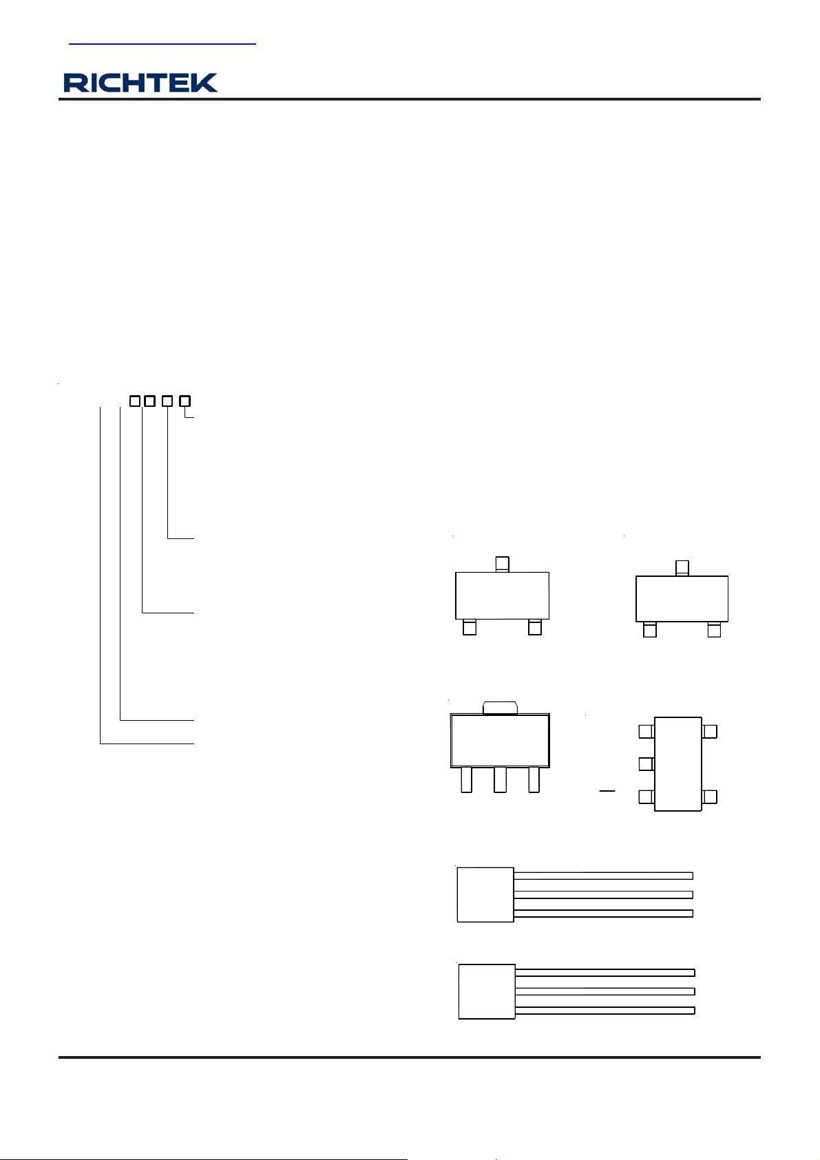
Pin Configurations
(TOP VIEW)
VIN
3
1
VOUT GND
SOT-23-3
2
VIN
3
1
GND VOUT
SOT-23-3 (L-Type)
2
Chip Enable High (SOT-23-5 Only)
Chip Enable Low
Note :
1. RT9169H package type is available in SOT-23-5 only.
2. RichTek Pb-free and Green products are :
`RoHS compliant and compatible with the current require ments of IPC/JEDEC J-STD-020.
`Suitable for use in SnPb or Pb-free soldering processes.
`100%matte tin (Sn) plating.
Marking Information
For marking information, contact our sales re presentative
directly or through a RichTek distributor located in your
area, otherwise visit our website for detail.
DS9169/H-12 March 2007 www.richtek.com
123
VIN
GND
SOT-89
VOUT
(TAB)
3
2
1
3
2
1
TO-92 (L-Type)
TO-92 (T-T ype)
VIN
GND
EN/EN
1
2
354
SOT-23-5
VOUT
GND
VIN
VOUT
NC
GND
VIN
VOUT
1
RT9169/H
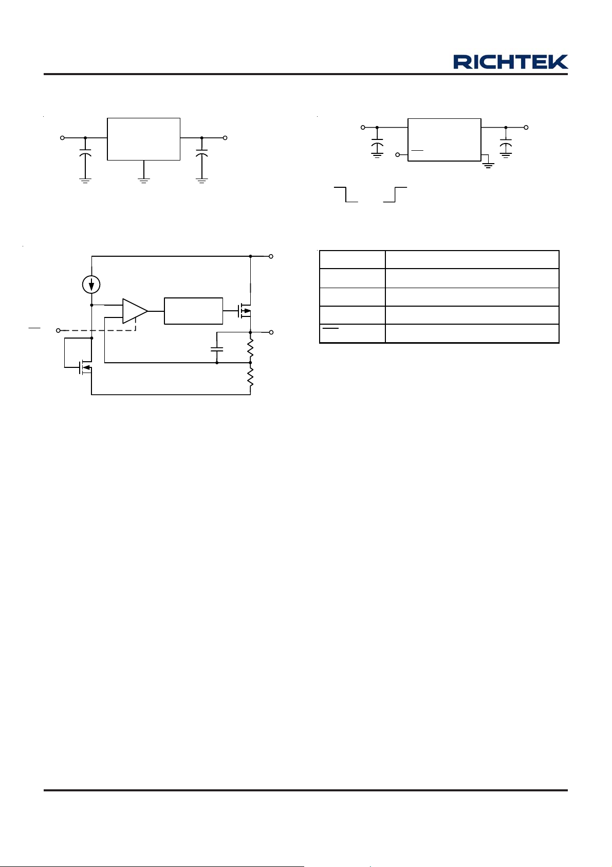
Typical Application Circuit
VIN
RT9169
VOUT
GND
C
1uF
+
IN
V
IN
Function Block Diagram
+
-
EN/EN
Current
Limit
+
C
1uF
OUT
V
OUT
VIN
VOUT
V
IN
C
1uF
RT9169
Chip Enable
+
IN
RT9169H
Chip Enable
VIN
RT9169/H
EN/EN
VOUT
GND
Functional Pin Description
Pin Name Pin Function
VIN Power Input
VOUT Output Voltage
GND Ground
EN/EN
Chip Enable Control Input
+
C
1uF
OUT
V
OUT
Absolute Maximum Ratings (Note 1)
z Input V oltage------------------------------------------------------------------------------------------------------------ 7V
z Power Dissipation, P
@ TA = 25°C
D
SOT-23-3 ---------------------------------------------------------------------------------------------------------------- 0.4W
SOT-23-5 ---------------------------------------------------------------------------------------------------------------- 0.4W
SOT- 89------------------------------------------------------------------------------------------------------------------- 0.571W
TO-92--------------------------------------------------------------------------------------------------------------------- 0.625W
z Junction T emperature------------------------------------------------------------------------------------------------- 150°C
z Lead Temperature (Soldering, 10 sec.)--------------------------------------------------------------------------- 260°C
z Storage T emperature Range ---------------------------------------------------------------------------------------- −65°C to 150°C
z Package Thermal Re sistance (Note 4)
SOT-23-3, θJA----------------------------------------------------------------------------------------------------------- 250°C/W
SOT-23-5, θJA----------------------------------------------------------------------------------------------------------- 250°C/W
SOT-89, θJA------------------------------------------------------------------------------------------------------------- 175°C/W
TO-92, θJA--------------------------------------------------------------------------------------------------------------- 160°C/W
z ESD Susceptibility (Note 2)
HBM (Human Body Mode) ------------------------------------------------------------------------------------------ 2kV
MM (Ma chine Mode)-------------------------------------------------------------------------------------------------- 200V
Recommended Operating Conditions (Note 3)
z Junction T emperature Range---------------------------------------------------------------------------------------- −40°C to 125°C
z Ambient T emperature Range---------------------------------------------------------------------------------------- −40°C to 85°C
DS9169/H-12 March 2007www.richtek.com
2
RT9169/H
Electrical Characteristics
(V
= 5.5V, CIN = 1μF, C
IN
Parameter Symbol Test Conditions Min Typ Max Units
Input Voltage Range VIN 2 -- 6 V
= 1μF, TA = 25°C, unless otherwise specified)
OUT
Output Voltage Accurac y ΔV
Maximum Output Current I
Current Limit I
IL = 1mA -2 -- +2 %
OUT
VIN = V
MAX
IL = 100mA 150 250 -- mA
LIM
+ 0.6V, VIN ≥ 3.6V 100 -- -- mA
OUT
No Load -- 4 7 μA
GND Pin Current IG
= 100mA 4 10 μA
I
OUT
I
= 1mA, VIN ≥ 3.6V -- 4 10
OUT
Dropout Voltage V
Line Regulation ΔV
Load Regulation ΔV
Output Noise eNO
DROP
I
OUT
I
OUT
V
LINE
V
LOAD ILOUT
BW = 100Hz to 50kHz
C
= 50mA, V
= 100mA, VIN ≥ 3.6V -- 450 600
= (V
IN
OUT
≥ 3.6V, I
IN
= 0mA to 100mA -- 0.01 0.04 %/mA
= 10μF
OUT
Ripple Rejection PSRR F = 1kHz, C
Standby
Current
EN/EN
Threshold
RT9169/H (SOT-23-5) EN = V
or EN = 0 -- 0.1 1 μA
IN
Logic High VIL 0.6 -- -Logic Low V
-- -- 2
IH
≥ 3.6V -- 200 300
IN
+ 0.3V) to 6V,
= 1mA
OUT
-0.2 -- +0.2 %/V
-- 250 -- μV
= 1μF -- 30 -- dB
OUT
mV
V
Thermal Shutdown Protection 125 -- -- °C
Note 1. Stresses listed as the above "Absolute Maximum Ratings" may cause permanent damage to the device. These are for
stress ratings. Functional operation of the device at these or any other conditions beyond those indicated in the
operational sections of the specifications is not implied. Exposure to absolute maximum rating conditions for extended
periods may remain possibility to affect device reliability.
Note 2. Devices are ESD sensitive. Handling precaution is highly recommended.
Note 3. The device is not guaranteed to function outside its operating conditions.
Note 4. θ
is measured in the natural convection at TA = 25°C on a low effective thermal conductivity test board of
JA
JEDEC 51-3 thermal measurement standard.
Application Information
A 1μF (or larger) capacitor is recommended between V
capa citor . Any type of ca pacitor ca n be used, but not Aluminum ele ctrolytes when operating below –25°C. The capa citance
may be increased without limit.
A 1μF capacitor (or larger) should be placed between VIN to GND.
DS9169/H-12 March 2007 www.richtek.com
and GND for stability. The part may oscillate without the
OUT
3

RT9169/H
)
)
Typical Operating Characteristics
Temperature Stab ility
3.7
V
OUT
3.3
2.9
2.5
Output Voltage (V)
2.1
V
OUT
1.7
-50 -25 0 25 50 75 100 125
Temperature
Dropout Voltage (VIN-V
0.8
0.7
0.6
0.5
0.4
0.3
(°C)
OUT
125°C
)
=
=
25°C
Quiescient Current vs. Temperature
5
4
μ
3
2
1
Quiescent Current ( A
0
-30 0 30 60 90 120
Temperature
VIN = 5V
(°C)
Short Circuit Current
500
400
300
200
25°C
125°C
0.2
Dropout Voltage (V)
0.1
0
020406080100
I
(mA)
LOAD
V
OUT
= 3.3V
PSRR
0
-10
-20
-30
-40
10mA
PSRR (dB)
-50
-60
-70
10 100 1k 10k 100k 1M
Frequency (Hz )
VIN = 5V, V
CIN = 1uF , TA = 125°C
C
= 1uF Electrolytic
OUT
Capacitor
OUT
50mA
=
100
Short Circuit Current (mA
0
012345
Inpu t/Output Differential (V)
PSRR
0
-10
OUT
50mA
=
-20
-30
-40
10mA
PSRR (dB)
-50
-60
-70
10 100 1k 10k 100k 1M
VIN = 5V, V
CIN = 1uF , TA = 125°C
C
= 1uF Electrolytic
OUT
Capacitor
Frequency (Hz)
DS9169/H-12 March 2007www.richtek.com
4

RT9169/H
300
V
I
OUT
200
100
Output Voltage
Deviation (mV)
0
≈ ≈
6
5
4
Deviation (V)
Input Voltage
3
V
V
20
TA = 25°C
0
−20
Output Voltage
Deviation (mV)
100
Line Transient Response
OUT
= 1.8V
= 50mA
Time (1ms/Div)
TA = 25°C
C
Load Transient Response
= 5V
IN
= 1.8V
OUT
= 1uF Electrolytic
OUT
C
= 1uF Ceramic
IN
C
= 1uF Ceramic
OUT
200
V
I
OUT
100
0
Output Voltage
Deviation (mV)
OUT
= 50mA
= 3.3V
TA = 25°C
C
= 1uF Electrolytic
OUT
≈ ≈
6
5
4
Deviation (V)
Input Voltage
Line Transient Response
3
Load Transient Response
V
= 5V
IN
V
= 1.8V
OUT
50
TA = 25°C
0
−50
Output Voltage
Deviation (mV)
≈
200
Time (1ms/Div)
C
C
= 1uF Ceramic
IN
= 1uF Ceramic
OUT
≈
50
Load
1
Current (mA)
−50
100
V
V
50
TA = 25°C
0
−50
Output Voltage
Deviation (mV)
100
50
Load
1
Current (mA)
−50
Time (500us/Div)
Load Transient Response
= 5V
IN
= 3.3V
OUT
Time (500us/Div)
C
= 1uF Ceramic
IN
C
= 1uF Ceramic
OUT
100
Load
10
Current (mA)
−100
Time (500us/Div)
100
50
0
−50
Output Voltage
≈
Deviation (mV)
≈ ≈
200
100
Load
10
Current (mA)
−100
Load Transient Response
V
= 5V
IN
V
= 3.3V
OUT
TA = 25°C
C
= 1uF Ceramic
IN
C
= 1uF Ceramic
OUT
Time (500us/Div)
DS9169/H-12 March 2007 www.richtek.com
5

RT9169/H
Outline Dimension
D
C
e
A
b
Dimensions In M illimeters Dimensions In Inches
Symbol
Min Max Min Max
A 0.889 1.295 0.035 0.051
A1 0.000 0.152 0.000 0.006
B
A1
H
L
B 1.397 1.803 0.055 0.071
b 0.356 0.508 0.014 0.020
C 2.591 2.997 0.102 0.118
D 2.692 3.099 0.106 0.122
e 1.803 2.007 0.071 0.079
H 0.080 0.254 0.003 0.010
L 0.300 0.610 0.012 0.024
SOT-23-3 Surface Mount Package
DS9169/H-12 March 2007www.richtek.com
6

RT9169/H
H
D
L
C
b
A
e
Dimensions In Millimeters Dimensions In Inches
Symbol
Min Max Min Max
A 0.889 1.295 0.035 0.051
A1 0.000 0.152 0.000 0.006
B 1.397 1.803 0.055 0.071
b 0.356 0.559 0.014 0.022
C 2.591 2.997 0.102 0.118
D 2.692 3.099 0.106 0.122
B
A1
e 0.838 1.041 0.033 0.041
H 0.080 0.254 0.003 0.010
L 0.300 0.610 0.012 0.024
SOT-23-5 Surface Mount Package
DS9169/H-12 March 2007 www.richtek.com
7

RT9169/H
D
D1
A
C
b1
e
b
e
A
b
Dimensions In Millimeters Dimensions In Inches
Symbol
Min Max Min Max
A 1.397 1.600 0.055 0.063
b 0.356 0.483 0.014 0.019
B 2.388 2.591 0.094 0.102
b1 0.406 0.533 0.016 0.021
C 3.937 4.242 0.155 0.167
B
C1
H
C1 0.787 1.194 0.031 0.047
D 4.394 4.597 0.173 0.181
D1 1.397 1.753 0.055 0.069
e 1.448 1.549 0.057 0.061
H 0.356 0.432 0.014 0.017
3-Lead SOT-89 Surface Mount Package
DS9169/H-12 March 2007www.richtek.com
8

RT9169/H
D
E
L
b
e
D1
A1
A
C
Symbol
Dimensions In M illimeters Dimensions In Inches
A 3.175 4.191
A1 1.143 1.372
b 0.406 0.533
C 0.406 0.533
D 4.445 5.207
D1 3.429 5.029
E 4.318 5.334
e 1.143 1.397
L
Richtek Technology Corporation
Headquarter
5F, No. 20, Taiyuen Street, Chupei City
Hsinchu, Taiwan, R.O.C.
Tel: (8863)5526789 Fax: (8863)5526611
Min Max Min Max
0.125 0.165
0.045 0.054
0.016 0.021
0.016 0.021
0.175 0.205
0.135 0.198
0.170 0.210
0.045 0.055
12.700
0.500
3-Lead TO-92 Plastic Package
Richtek Technology Corporation
Taipei Office (Marketing)
8F, No. 137, Lane 235, Paochiao Road, Hsintien City
Taipei County, Taiwan, R.O.C.
Tel: (8862)89191466 Fax: (8862)89191465
Email: marketing@richtek.com
DS9169/H-12 March 2007 www.richtek.com
9
 Loading...