


Preliminary
RT9169
100mA, 4µµµµA Quiescent Current CMOS LDO Regulator
General Description
The RT9169 series are 100mA ultra-low quiescent
current CMOS low dropout (LDO) regulator designed
for battery-powered equipments. The output voltages
range from 1.2V to 5V with 0.1V per step.
The other features include 4µA ultra-low quiescent,
low dropout voltage, high output accuracy, current
limiting protection, and high ripple rejection ratio.
Ordering Information
RT9169-
Package type
ZL : TO-92 L Type
ZT : TO-92 T Type
X : SOT-89
V : SOT-23
CB : SOT-25
Operating temperature range
C: Commercial standard
Output voltage
12 : 1.2V
13 : 1.3V
:
49 : 4.9V
50 : 5.0V
Features
z
Ultra-Low Quiescent Current: 4µµµµA
Low Dropout: 450mV at 100mA
z
Wide Operating Voltage Ranges: 2V~6V
z
Current Limiting Protection
z
Only 1µµµµF Output Capacitor Required for
z
Stability
High Power Supply Rejection Ratio
z
Applications
z Battery-Powered Equipment
z Palmtops, Notebook Computers
z Hand-held Instruments
z PCMCIA Cards
Pin Configurations
Part Number Pin Configurations
RT9169-CZL
(Plastic TO-92)
RT9169-CZT
(Plastic TO-92)
TOP VIEW
1. VIN
2. GND
3. VOUT
TOP VIEW
1. VOUT
2. VIN
3. GND
Typical Application Circuit
RT9169-CX
(Plastic SOT-89)
RT9169
C
OUT
1µF
V
OU T
RT9169-CV
(Plastic SOT-23)
V
IN
C
IN
1µF
VIN
GND
VOUT
RT9169-CB
123
3
2
1
5
4
(Plastic SOT-25)
3
21
DS9169-02 October 2001 www.richtek-ic.com.tw
TOP VIEW
1. GND
2. VIN (TAB)
3. VOUT
TOP VIEW
1. VOUT
2. GND
3. VIN
TOP VIEW
1. VIN
2. GND
3. EN
4. NC
5. VOUT
1

RT9169
Marking Information
Preliminary
Part Number Marking
RT9169-12CX B1
RT9169-13CX B2
RT9169-14CX B3
RT9169-15CX B4
RT9169-16CX B5
RT9169-17CX B6
RT9169-18CX B7
RT9169-19CX B8
RT9169-20CX B9
RT9169-21CX BA
RT9169-22CX BB
RT9169-23CX BC
RT9169-24CX BD
RT9169-25CX BE
RT9169-26CX BF
RT9169-27CX BG
Part Number Marking
RT9169-48CX C4
RT9169-49CX C5
RT9169-50CX C6
RT9169-12CZL RTD1
RT9169-13CZL RTD2
RT9169-14CZL RTD3
RT9169-15CZL RTD4
RT9169-16CZL RTD5
RT9169-17CZL RTD6
RT9169-18CZL RTD7
RT9169-19CZL RTD8
RT9169-20CZL RTD9
RT9169-21CZL RTDA
RT9169-22CZL RTDB
RT9169-23CZL RTDC
RT9169-24CZL RTDD
RT9169-28CX BH
RT9169-29CX BJ
RT9169-30CX BK
RT9169-31CX BL
RT9169-32CX BM
RT9169-33CX BN
RT9169-34CX BP
RT9169-35CX BQ
RT9169-36CX BR
RT9169-37CX BS
RT9169-38CX BT
RT9169-39CX BU
RT9169-40CX BV
RT9169-41CX BW
RT9169-42CX BX
RT9169-43CX BY
RT9169-44CX BZ
RT9169-25CZL RTDE
RT9169-26CZL RTDF
RT9169-27CZL RTDG
RT9169-28CZL RTDH
RT9169-29CZL RTDJ
RT9169-30CZL RTDK
RT9169-31CZL RTDL
RT9169-32CZL RTDM
RT9169-33CZL RTDN
RT9169-34CZL RTDP
RT9169-35CZL RTDQ
RT9169-36CZL RTDR
RT9169-37CZL RTDS
RT9169-38CZL RTDT
RT9169-39CZL RTDU
RT9169-40CZL RTDV
RT9169-41CZL RTDW
RT9169-45CX C1
RT9169-46CX C2
RT9169-47CX C3
www.richtek-ic.com.tw DS9169-02 October 2001
RT9169-42CZL RTDX
RT9169-43CZL RTDY
RT9169-44CZL RTDZ
2

Preliminary
RT9169
Part Number Marking
RT9169-45CZL RTC1
RT9169-46CZL RTC2
RT9169-47CZL RTC3
RT9169-48CZL RTC4
RT9169-49CZL RTC5
RT9169-50CZL RTC6
RT9169-12CZT RTE1
RT9169-13CZT RTE2
RT9169-14CZT RTE3
RT9169-15CZT RTE4
RT9169-16CZT RTE5
RT9169-17CZT RTE6
RT9169-18CZT RTE7
RT9169-19CZT RTE8
RT9169-20CZT RTE9
RT9169-21CZT RTEA
Part Number Marking
RT9169-43CZT RTEY
RT9169-44CZT RTEZ
RT9169-45CZT RTC7
RT9169-46CZT RTC8
RT9169-47CZT RTC9
RT9169-48CZT RTCA
RT9169-49CZT RTCB
RT9169-50CZT RTCC
RT9169-12CV B1
RT9169-13CV B2
RT9169-14CV B3
RT9169-15CV B4
RT9169-16CV B5
RT9169-17CV B6
RT9169-18CV B7
RT9169-19CV B8
RT9169-22CZT RTEB
RT9169-23CZT RTEC
RT9169-24CZT RTED
RT9169-25CZT RTEE
RT9169-26CZT RTEF
RT9169-27CZT RTEG
RT9169-28CZT RTEH
RT9169-29CZT RTEJ
RT9169-30CZT RTEK
RT9169-31CZT RTEL
RT9169-32CZT RTEM
RT9169-33CZT RTEN
RT9169-34CZT RTEP
RT9169-35CZT RTEQ
RT9169-36CZT RTER
RT9169-37CZT RTES
RT9169-38CZT RTET
RT9169-20CV B9
RT9169-21CV BA
RT9169-22CV BB
RT9169-23CV BC
RT9169-24CV BD
RT9169-25CV BE
RT9169-26CV BF
RT9169-27CV BG
RT9169-28CV BH
RT9169-29CV BJ
RT9169-30CV BK
RT9169-31CV BL
RT9169-32CV BM
RT9169-33CV BN
RT9169-34CV BQ
RT9169-35CV BR
RT9169-36CV BS
RT9169-39CZT RTEU
RT9169-40CZT RTEV
RT9169-41CZT RTEW
RT9169-42CZT RTEX
DS9169-02 October 2001 www.richtek-ic.com.tw
RT9169-37CV BT
RT9169-38CV BU
RT9169-39CV BV
RT9169-40CV BW
3

RT9169
Preliminary
Part Number Marking
RT9169-41CV BX
RT9169-42CV BY
RT9169-43CV BZ
RT9169-44CV CT
RT9169-45CV CU
RT9169-46CV CV
Pin Description
Pin Name Pin Function
VIN Power Input
VOUT Output Voltage
GND Ground
EN Chip Enable Control Input
Function Block Diagram
Part Number Marking
RT9169-47CV CW
RT9169-48CV CX
RT9169-49CV CY
RT9169-50CV CZ
RT9169-25CB C1
RT9169-28CB C2
VIN
+
_
EN
Current
Lim it
VOUT
GND
Absolute Maximum Ratings
Input Voltage 7V
z
Power Dissipation, PD @ TA = 25° C
z
TO-92 0.6W
SOT-89 0.5W
SOT-23 0.25W
SOT-25 0.25W
Operating Junction Temperature Range -40°C to 125°C
z
Storage Range -65°C to 150°C
z
Package Thermal Resistance
z
TO-92, θ
SOT-89, θ
SOT-89, θ
SOT-23, θ
SOT-25, θ
JA
JC
JA
JA
JA
160°C/W
100°C/W
300°C/W
250°C/W
250°C/W
www.richtek-ic.com.tw DS9169-02 October 2001
4

Electrical Characteristics
(V
= 5.5V, CIN = 1µF, C
IN
Parameter Symbol Test Conditions Min Typ Max Units
= 1µF, TA = 25°C, unless otherwise specified)
OUT
Preliminary
RT9169
Input Voltage Range
Output Voltage Accuracy
Maximum Output Current
Current Limit
V
IN
∆V
OUTIL
I
MAX
I
LIMIT
= 1mA
VIN = V
R
LOAD
No Load -- 4 7
GND Pin Current
Dropout Voltage
Line Regulation
Load Regulation
Output Noise
Ripple Rejection PSRR
I
G
V
DROP
∆V
LINE
∆V
LOADILOUT
e
NO
I
= 100mA
OUT
I
= 1mA, VIN ≥ 3.6V
OUT
I
= 50mA, VIN ≥ 3.6V
OUT
I
= 100mA, VIN ≥ 3.6V
OUT
VIN = (V
V
≥ 3.6V, I
IN
= 0mA to 100mA
BW = 100Hz to 50KHz
C
= 10µF
OUT
F = 1KHz, C
Standby Current RT9169-CB EN = V
+ 0.6V, VIN ≥ 3.6V
OUT
= 1Ω
+ 0.3V) to 6V,
OUT
= 1mA
OUT
= 10µF
OUT
IN
2--6V
-2 -- +2 %
100 -- -- mA
-- 250 -- mA
µA
410
µA
-- 4 --
-- 200 --
mV
-- 450 --
-0.2 -- +0.2 %/V
-- 0.01 0.04 %/mA
-- 250 --
µV
-- 50 -- DB
-- 0.1 1 µA
EN Threshold 0.6 1 2 V
Application Information
A 1µF (or larger) capacitor is recommended between
VOUT and GND for stability. The part may oscillate
without the capacitor. Any type of capacitor can be
used, but not Aluminum electrolytes when operating
below –25°C. The capacitance may be increased
without limit.
A 1µF capacitor (or larger) should be placed between
VIN to GND.
DS9169-02 October 2001 www.richtek-ic.com.tw
5
RT9169
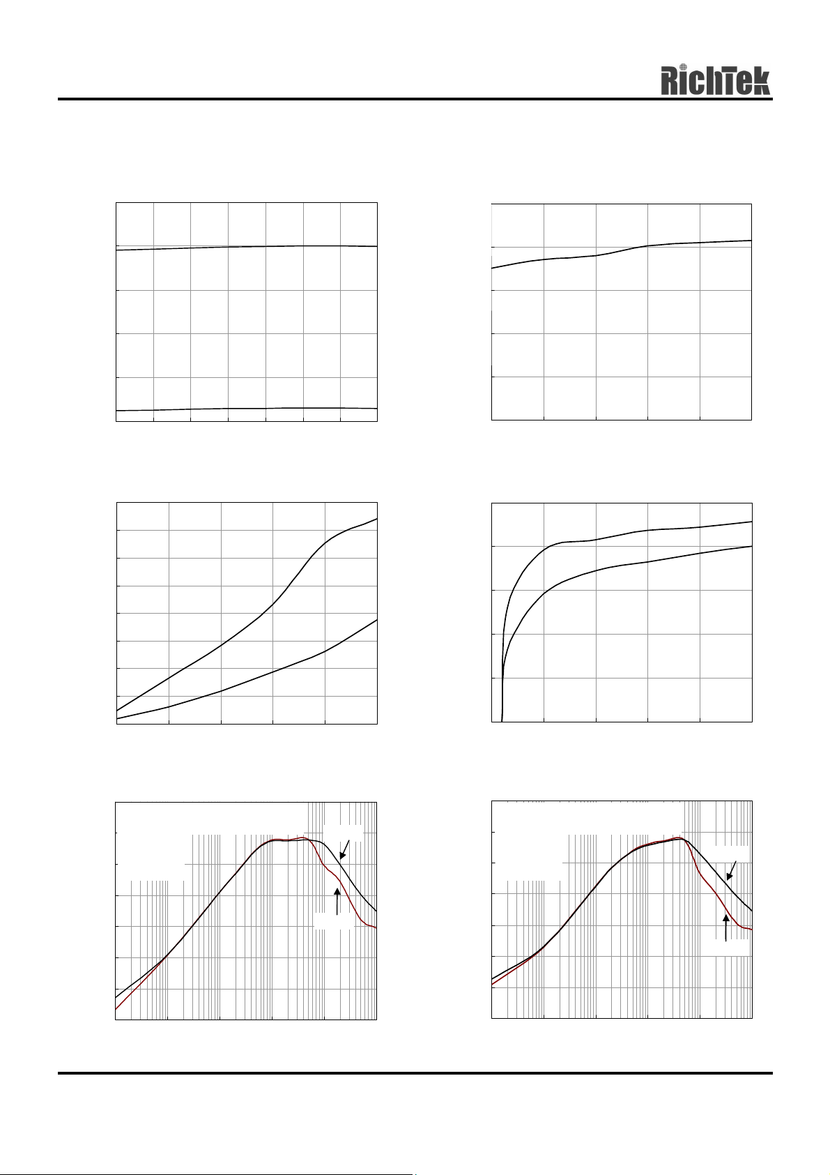
Typical Operating Charateristics
Preliminary
3.7
Temperature Stability
V
3.3
2.9
2.5
Output Voltage (V)
2.1
1.7
-50 -25 0 25 50 75 100 125
Temperature ( C)
Dropout Voltage (VIN-V
0.8
0.7
0.6
0.5
0.4
0.3
OUT
V
OUT
°
OUT
= 3.3V
= 1.8V
)
125°C
25°C
5
4
3
µ
I ( A)
2
1
VIN = 5V
Quiescient Current
0
-30 0 30 60 90 120
Temperature ( C)
°
Short Circuit Current
500
400
125°C
300
200
25°C
Dropout Voltage (V)
0.2
0.1
V
0
0 20 40 60 80 100
I
(mA)
LOAD
OUT
PSRR
0
CIN = 1µF
C
= 1µF Electrolytic Capacitor
OUT
-10
VIN = 5V
= 1.8V
V
OUT
-20
TA = 25°C
-30
-40
PSRR (dB)
-50
-60
-70
10 100 1K 10K 100K 1M
Frequenc y (Hz)
10mA
= 3.3V
50mA
100
Short Circuit Current (mA)
0
012345
Input/Output Diff erential (V)
PSRR
0
CIN = 1µF
C
= 1µF Electrolytic Capacitor
OUT
-10
VIN = 5V
= 3.3V
V
OUT
-20
TA = 25°C
-30
-40
PSRR (dB)
-50
-60
-70
10 100 1K 10K 100K 1M
Frequenc y (Hz)
50mA
10mA
www.richtek-ic.com.tw DS9169-02 October 2001
6

>
>
>2 >
>
>
(
)
>
>
>2 >
>
>
≈
(
)
≈
>
>
>2 >
>
>
≈
(
)
≈
>
>
>2 >
>
>
≈
(
)
≈
T
T
>
>
>2 >
>
>
≈
(
)
≈
>
>
>2 >
>
>
(
)
Preliminary
RT9169
Output Voltage
Input Voltage
Output Voltage
Line Transient Response
300
V
= 1.8V
OUT
200
mV
= 25°C
T
A
100
2
2 >2
0
T
Deviation
-100
≈
6
5
1
1
1 >1
T
4
Deviation (V)
0 1 2 3 4 5 6 7 8 9 10
C
OUT
= 50mA
I
OUT
Time (mS)
= 1µF Electrolytic
Load Transient Response
60
CIN = 1µF Electrolytic
mV
40
C
= 1µF Electrolytic
OUT
= 25°C
T
A
20
Deviation
2
0
2 >2
T
VIN = 5V
V
OUT
= 1.8V
≈
Line Transient Response
300
V
= 3.3V
OUT
200
= 25°C
T
mV
A
100
2
2 >2
0
Deviation
Output Voltage
T
-100
≈
6
5
1
1
1 >1
T
4
Deviation (V)
Input Voltage
0 1 2 3 4 5 6 7 8 9 10
C
OUT
= 50mA
I
OUT
Time (mS)
= 1µF Electrolytic
Load Transient Response
300
CIN = 1µF Electrolytic
mV
200
C
= 1µF Electrolytic
OUT
= 25°C
T
A
100
Output Voltage
Deviation
2
2 >2
0
T
VIN = 5V
V
= 1.8V
OUT
≈
Load Current (mA)
Output Voltage
Load Current (mA)
-20
50
1
1
1 >1
1
-50
Load Transient Response
60
CIN = 1µF Electrolytic
mV
40
C
= 1µF Electrolytic
OUT
= 25°C
T
A
20
Deviation
2
0
2 >2
-20
50
1
1
1 >1
1
-50
T
Time (100µS)
Time (100µS)
VIN = 5V
= 3.3V
V
OUT
Output Voltage
Load Current (mA)
-100
100
1
1
1 >1
10
-100
Load Current (mA)
Load Transient Response
300
CIN = 1µF Electrolytic
mV
200
C
= 1µF Electrolytic
OUT
= 25°C
T
A
100
Deviation
2
2 >2
0
-100
100
1
1
1 >1
10
-100
T
Time (100µS)
T
T
Time (100µS)
VIN = 5V
V
= 3.3V
OUT
DS9169-02 October 2001 www.richtek-ic.com.tw
7

RT9169
Package Information
D
Preliminary
E
L
A
b
e e
D1
Symbol
A 3.175 4.191
A1 1.143 1.372
b 0.406 0.533
C 0.406 0.533
D 4.445 5.207
D1 3.429 --
Dimensions In Millimeters Dimensions In Inches
Min Max Min Max
A1
C
0.125 0.165
0.045 0.054
0.016 0.021
0.016 0.021
0.175 0.205
0.135 --
E 4.318 5.334
e 1.143 1.397
L 12.700 --
3-Lead TO-92 Package
www.richtek-ic.com.tw DS9169-02 October 2001
0.170 0.210
0.045 0.055
0.500 --
8

Preliminary
RT9169
D
D1
C
C1
e e
b
b1 b
B
A
A
H
Symbol
A 1.397 1.600 0.055 0.063
b 0.356 0.483 0.014 0.019
B 2.388 2.591 0.094 0.102
b1 0.406 0.533 0.016 0.021
C -- 4.242 -- 0.167
C1 0.787 1.194 0.031 0.047
D 4.394 4.597 0.173 0.181
D1 1.397 1.753 0.055 0.069
e 1.448 1.549 0.057 0.061
H 0.381 0.432 0.015 0.017
Dimensions In Millimeters Dimensions In Inches
Min Max Min Max
3-Lead SOT-89 Surface Mount
DS9169-02 October 2001 www.richtek-ic.com.tw
9

RT9169
Preliminary
D
A1
B
L
C
e
A
b
Dimensions In Millimeters Dimensions In Inches
Symbol
Min Max Min Max
A 0.889 1.295 0.035 0.051
A1 -- 0.152 -- 0.006
B 1.397 1.803 0.055 0.071
H
b 0.356 0.508 0.014 0.020
C 2.591 2.997 0.102 0.118
D 2.692 3.099 0.106 0.122
e 1.803 2.007 0.071 0.079
H 0.102 0.254 0.004 0.010
L 0.356 0.610 0.014 0.024
SOT-23 Plastic Surface Mount
www.richtek-ic.com.tw DS9169-02 October 2001
10

D
Preliminary
RT9169
C
b
A
e
Symbol
A 0.889 1.295 0.035 0.051
A1 0.000 0.152 0.000 0.006
B 1.397 1.803 0.055 0.071
B
A1
Dimensions In Millimeters Dimensions In Inches
Min Max Min Max
H
L
b 0.356 0.559 0.014 0.022
C 2.591 2.997 0.102 0.118
D 2.692 3.099 0.106 0.122
e 0.838 1.041 0.033 0.041
H 0.102 0.254 0.004 0.010
L 0.356 0.610 0.014 0.024
SOT- 25 Surface Mount Package
DS9169-02 October 2001 www.richtek-ic.com.tw
11

RT9169
Preliminary
RICHTEK TECHNOLOGY CORP.
Headquarter
6F, No. 35, Hsintai Road, Chupei City
Hsinchu, Taiwan, R.O.C.
Tel: (8863)5510047 Fax: (8863)5537749
www.richtek-ic.com.tw DS9169-02 October 2001
RICHTEK TECHNOLOGY CORP.
Taipei Office (Marketing)
8F-1, No. 137, Lane 235, Paochiao Road, Hsintien City
Taipei County, Taiwan, R.O.C.
Tel: (8862)89191466 Fax: (8862)89191465
Email: marketing@richtek-ic.com.tw
12
 Loading...