

RT9167/A
Low-Noise, Fixed Output Voltage,300mA/500mA LDO Regulator
General Description
The RT9167/A is a 300mA/500mA low dropout and low
noise micropower regulator suitable for portable
a pplications. The output voltages ra nge from 1.5V to 5V
in 100mV increments a nd 2% accura cy . The RT9167/A is
designed for use with very low ESR ca pa citors. The output
remains stable even with 1μF cera mic output ca pa citor.
The RT9167/A use s a n intern al P-MOSFET as the pa ss
device, which does not cause extra GND current in heavy
load and dropout condition s. The shutdown mode of nearly
zero operation current makes the IC suitable f or batterypowered devices. Other features include a reference
bypass pin to improve low noise performance, current
limiting, and over te mperature protection.
Ordering Information
RT9167/A-
Package Type
B : SOT-23-5
BR : SOT-23-5 (R-Type)
S : SOP-8
Lead Plating System
P : Pb Free
G : Green (Halogen Free and Pb Free)
Output Voltage
15 : 1.5V
16 : 1.6V
:
49 : 4.9V
50 : 5.0V
2H : 2.85V
500mA Output Current
300mA Output Current
Note :
Richtek products are :
` RoHS compliant and compatible with the current require-
ments of IPC/JEDEC J-STD-020.
` Suitable for use in SnPb or Pb-free soldering processes.
Features
zz
Stable with Low-ESR Output Capacitor
z
zz
zz
z Low Dropout Voltage (350mV @ 300mA)
zz
−−
zz
z Low Operation Current
zz
zz
z Shutdown Function
zz
zz
z Low Noise Output
zz
zz
z Low Temperature Coefficient
zz
zz
z Current and Thermal Limiting
zz
zz
z Custom Voltage Available
zz
zz
z SOT-23-5 a nd SOP-8 Packages
zz
zz
z RoHS Compliant and 100% Lead (Pb)-Free
zz
μμ
−80
μA Typical
−−
μμ
Applications
z Cellular T elephones
z Laptop, Notebook, a nd Palmtop Computers
z Battery-powered Equipment
z Hand-held Equi pment
Marking Information
For marking information, conta ct our sales representative
directly or through a Richtek distributor located in your
area.
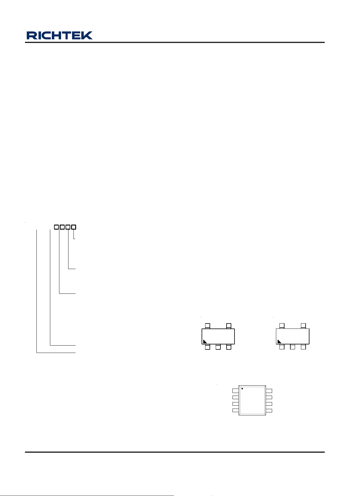
Pin Configurations
(TOP VIEW)
VOUT
5
VIN
GND
SOT-23-5
BP
4
23
EN
EN
VIN
VOUT
BP
8
2
3
4
7
6
5
BP
5
VOUT GND
EN
4
23
VIN
SOT-23-5 (R-T ype)
GND
GND
GND
GND
SOP-8
DS9167/A-29 April 2011 www.richtek.com
1
RT9167/A
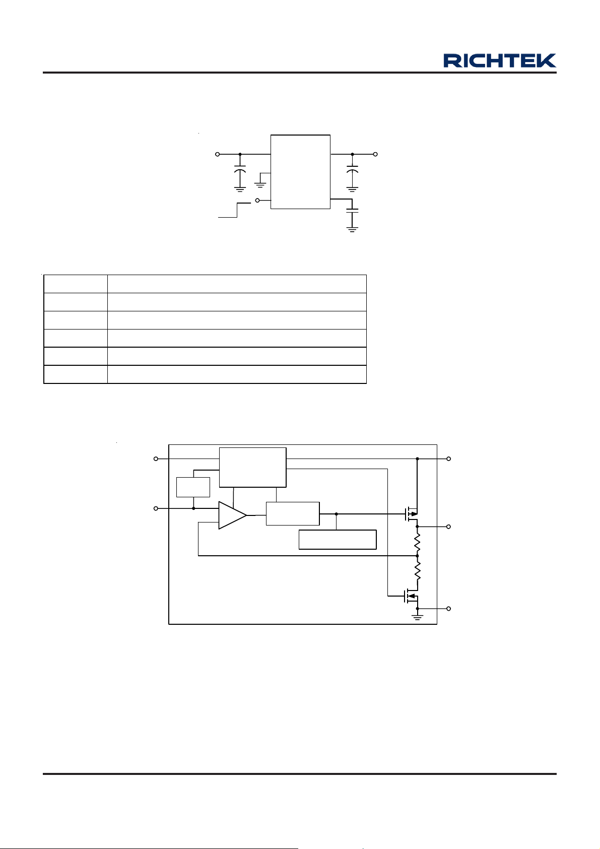
Typical Application Circuit
V
IN
Chip Enable
Functional Pin Description
Pin Name Pin Function
VIN Power Input Voltage
GND Ground
EN Chip Enable (Active High)
BP Reference Noise Bypass
VOUT Output Voltage
Function Block Diagram
C
1µF
+
IN
RT9167/A
IN
GND
EN BP
OUT
+
C
C
10nF
OUT
1µF
BP
V
OUT
EN
BP
VREF
Shutdown
and
Logic Control
+
-
Error
Amplifier
MOS Driver
Thermal Protection
VIN
VOUT
Current-Limit and
R1
R2
GND
DS9167/A-29 April 2011www.richtek.com
2
RT9167/A
Absolute Maximum Ratings
z Input V oltage ---------------------------------------------------------------------------------------------------------- 8V
z Power Dissipation, P
SOT-23-5--------------------------------------------------------------------------------------------------------------- 0.4W
SOP-8 ------------------------------------------------------------------------------------------------------------------ 0.625W
z Package Thermal Resista nce (Note1)
SOT-23-5, θJA--------------------------------------------------------------------------------------------------------- 250°C/W
SOT-23-5, θJC--------------------------------------------------------------------------------------------------------- 130°C/W
SOP-8, θJA------------------------------------------------------------------------------------------------------------ 160°C/W
SOP-8, θJC------------------------------------------------------------------------------------------------------------ 60°C/W
z Operating Junction T emperature Ra nge------------------------------------------------------------------------- −40°C to 125°C
z Storage T emperature Range --------------------------------------------------------------------------------------- −65°C to 150°C
z Lead T emperature (Soldering, 10 sec.) ------------------------------------------------------------------------- 260°C
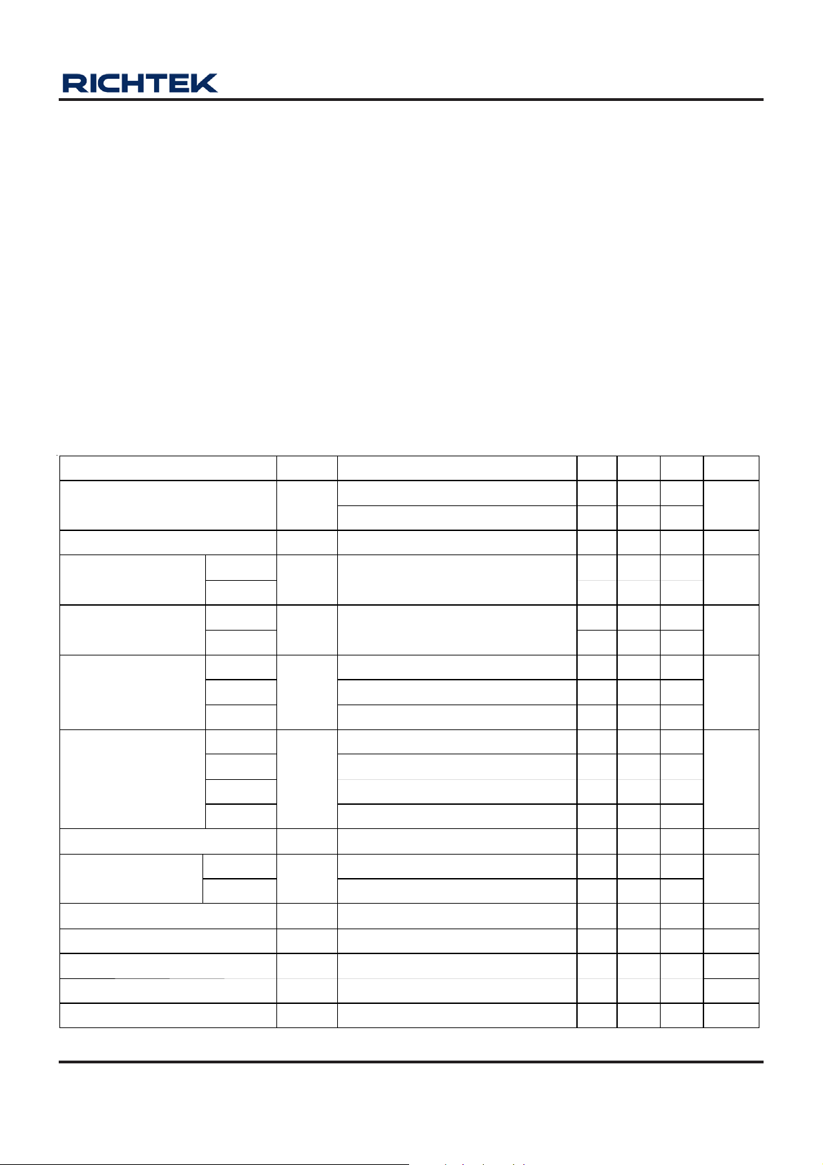
Electrical Characteristics
(V
= 5.0V, C
IN
= 1μF, C
IN
Parameter Symbol Test Conditions Min Typ Max Unit
@ TA = 25°C
D
= 1μF, T
OUT
= 25° C, unless otherwise specified)
A
Input Voltage Range
Output Voltage Accuracy
Maximum Output
Current
RT9167 300 -- -RT9167A
RT9167 400 -- --
Current Limit
RT9167A
RT9167/A No Load -- 80 150
Quiescent Current
RT9167/A
RT9167A
RT9167/A
Dropout Voltage
(V
OUT(Norm al)
Version)
(2)
= 3.0V
RT9167/A
RT9167/A
RT9167A
Line Regulation
RT9167/A
Load Regulation
RT9167A
EN Input High Threshold
EN Input Low Threshold
EN Bias Curr ent
Shutdown Supply Current
Thermal Shutdown Temp erature
2.9 -- 7
V
IN
ΔV
OUT
I
MAX
R
I
LIM
I
G
V
DROP
ΔV
LINE
ΔV
LOAD
V
VIN= 3V to 5.5V
IH
VIN = 3V to 5.5V
V
IL
I
SD
I
GSD
T
SD
= 50mA
I
L
IL = 1mA
= 1Ω
LOAD
= 300mA
I
OUT
I
= 500mA
OUT
= 1mA
I
OUT
= 50mA
I
OUT
VIN= (V
V
= 300mA
I
OUT
= 500mA
I
OUT
OUT
= 0mA to 300mA
I
OUT
= 0mA to 500mA
I
OUT
= 0V
OUT
-- 155 --
+0.15) to 7V, I
-- -- 100 nA
OUT
=1m A
2.7 -- 7
V
-2 -- 2 %
mA
500 -- --
mA
500 700 --
-- 90 150
μA
-- 90 150
-- 1.1 5
-- 55 100
mV
-- 350 450
-- 600 750
-- -- 6 mV/V
-- -- 30
mV
-- -- 35
1.6 -- -- V
-- -- 0.4 V
-- 0.01 1 μA
°C
T o be continued
DS9167/A-29 April 2011 www.richtek.com
3

RT9167/A
Parameter Symbol Test Conditions Min Typ Max Unit
Output Noise
Rippl e Rejection PSRR
Note 1. θJA is measured in the natural convection at TA = 25°C on a low effective thermal conductivity test board of
JEDEC 51-3 thermal measurement standard. Pin 1 of SOP-8 and pin4 of SOT-23-5 packages are the case position for
measurement.
θ
JA
Note 2. The dropout voltage is defined as V
CBP = 10nF, C
e
NO
F = 100Hz, C
-V
IN
, which is measured when V
OUT
= 10μF
OUT
= 10nF , C
BP
OUT
OUT
= 10μF
is V
-- 350 -- nV
-- 58 --
OUT(NORMAL)
− 100mV.
dB
Hz
DS9167/A-29 April 2011www.richtek.com
4
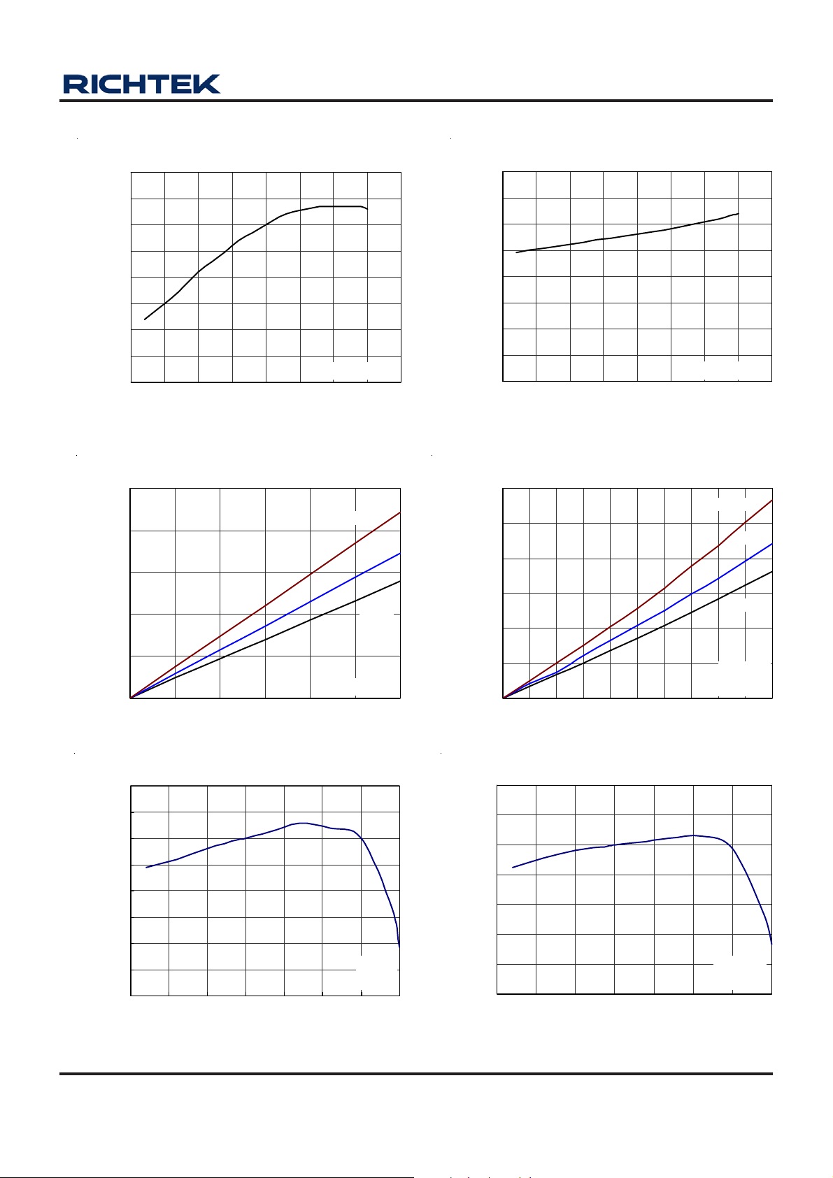
Typical Operating Characteristics
RT9167/A
Output Voltage vs. Temperature
3.33
3.32
3.31
3.30
3.29
3.28
Output Voltage (V)
3.27
3.26
3.25
-50 -25 0 25 50 75 100 125 150
Temperature
V
(°C)
Dropout Voltage vs. Load Current
250
200
150
100
Drop out Volt age (mV)
50
0
0 0.05 0.1 0.15 0.2 0.25 0.3
Load C urrent (A)
= 3.3V
OUT
125°C
RT9167
V
OUT
25°C
-40°C
= 5V
Quiescent Current vs. Temperature
120
105
90
75
60
45
30
Quiescent Current (uA)1
15
0
-50 -25 0 25 50 75 100 125 150
Temperature
(°C)
V
OUT
Dropout Voltage vs. Load Current
600
500
400
300
200
Dropou t V oltage ( m V)
100
V
0
0 0.05 0.1 0.15 0.2 0.25 0.3 0.35 0.4 0.45 0.5
Load Current (A)
OUT
= 3.3V
125°C
25°C
-40°C
RT9167A
= 3.3V
Current Limit vs. Temperature
700
650
600
550
500
450
Current Li m it (m A )
400
350
300
-50 -25 0 25 50 75 100 125
Temperature
(°C)
V
OUT
RT9167
= 5V
900
800
700
600
500
400
Current Li m it (m A )
300
200
-50-250 255075100125
Current Limit vs. Temperature
RT9167A
V
= 3.3V
OUT
Temperature
(°C)
DS9167/A-29 April 2011 www.richtek.com
5
RT9167/A
60
C
C
40
C
20
0
Output Voltage
Deviation (mV)
-20
≈ ≈
50
(mA)
1
Load Current
-50
150
V
C
100
CBP = 10nF
50
Load Transient Response
= 10μF
IN
= 1μF
OUT
= 10nF
BP
Time (50μs/Div)
Line Transient Response
= 3V
OUT
= 1μF
OUT
V
= 4V
IN
= 3V
V
OUT
Loading = 1mA
60
C
C
40
CBP = 10nF
20
0
Output Voltage
Deviation (mV)
-20
≈ ≈
50
(mA)
1
Load Current
-50
150
V
OUT
C
100
50
OUT
CBP = 10nF
Load Transient Response
= 10μF
IN
= 4.7μF
OUT
Time (50μs/Div)
Line Transient Response
= 3V
= 1μF
V
= 4V
IN
= 3V
V
OUT
Loading = 50mA
0
Output Voltage
Deviation (mV)
-50
≈ ≈
5
4
Deviation (V)
Input Voltage
150
V
C
100
CBP = 10nF
50
0
Output Voltage
Deviation (mV)
-50
≈ ≈
5
Time (1ms/Div)
Line Transient Response
= 3V
OUT
= 4.7μF
OUT
Loading = 1mA
0
Output Voltage
Deviation (mV)
-50
≈ ≈
5
4
Deviation (V)
Input Voltage
60
V
C
40
CBP = 10nF
20
0
Output Voltage
Deviation (mV)
-20
≈ ≈
5
Time (1ms/Div)
Line Transient Response
= 3V
OUT
= 4.7μF
OUT
Loading = 50mA
6
4
Deviation (V)
Input Voltage
Time (500μs/Div)
4
Deviation (V)
Input Voltage
Time (500μs/Div)
DS9167/A-29 April 2011www.richtek.com
RT9167/A
70
PSRR
60
50
40
30
PSRR (dB)
20
10
0
10 100 1K 10K 100K 1M
10 100 1000 10000 100000 1000000
V
= 3.3V, I
OUT
C
= 4.7μF, CBP = 10nF
OUT
Frequency (k Hz)
LOAD
= 1mA
DS9167/A-29 April 2011 www.richtek.com
7

RT9167/A
Voltage (0.5V / DIV)
Application Information
Capacitor Selection and Regulator Stability
Like any low-dropout regulator , the external ca pacitors used
with the RT9167/A must be carefully selected for regulator
stability and perf ormance.
Using a capa citor whose value is > 1μF on the RT9167/A
input and the amount of capacitance can be increased
without limit. The input capacitor must be located a
distance of not more than 0.5" from the in put pin of the IC
and returned to a clea n an alog ground. Any good quality
ceramic or tantalum can be used for this capacitor. The
ca pacitor with larger value and lower ESR (equivalent series
resistance) provides better PSRR and line-transient
response.
The output capacitor must meet both requirements for
minimum amount of capacitance and ESR in all LDOs
application. The RT9167/A is designed spe cifically to work
with low ESR ceramic output capacitor in space-saving
and performa nce consideration. Using a cera mic ca pacitor
whose value is at least 1μF with ESR is > 5mΩ on the
RT9167/A output ensures stability. The RT9167/A still
works well with output ca pacitor of other type s due to the
wide stable ESR range. Figure 1. shows the curves of
allowable ESR range a s a function of load current for various
output voltages and ca pa citor values. Output ca pacitor of
larger capacitance can reduce noise and improve loadtransient response, stability, and PSRR. The output
Region of Stable C
100.000
100
10.000
10
(Ω)
1.000
1
ESR ( )
0.100
0.1
OUT
C
Unstable Region
Stable Region
ESR vs. Load Current
OUT
C
OUT
= 1μF
capacitor should be located not more than 0.5" from the
V
pin of the RT9167/A and returned to a clea n a nalog
OUT
ground.
Note that some ceramic dielectrics exhibit large
capa cita nce a nd ESR vari ation with temperature. It may
be necessary to use 2.2μF or more to ensure stability at
temperatures below −10°C in this case. Also, tantalum
capacitors, 2.2μF or more may be needed to maintain
capacitance and ESR in the stable region for strict
application environ ment.
Tantalum capacitors maybe suffer failure due to surge
current when it is connected to a low-impedance source
of power (like a battery or very large capa citor). If a ta ntalum
capacitor is used at the input, it must be guaranteed to
have a surge current rating sufficient for the application
by the manufa cture.
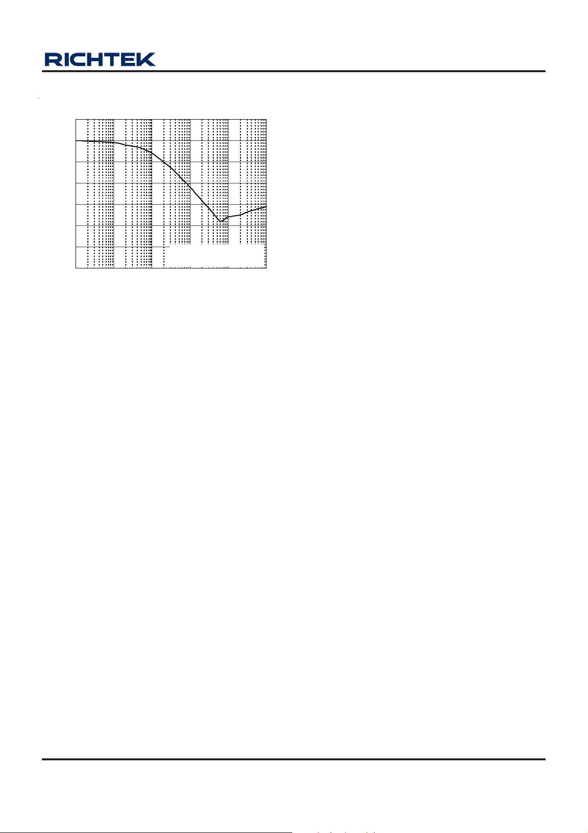
Use a 10nF bypass ca pa citor at BP f or low output voltage
noise. The ca pacitor , in conjunction with an intern al 200kΩ
resistor, which connects bypass pin and the band-gap
reference, creates an 80Hz low-pass filter for noise
reduction. Increa sing the capa citance will slightly de crease
the output noise, but increase the start-up time. The
ca pacitor connected to the bypa ss pin f or noise reduction
must have very low leakage. This capa citor leakage current
causes the output voltage to decline by a proportional
amount to the current due to the voltage drop on the intern al
200kΩ resistor. Figure 2 shows the power on respon se.
C
= 10nF
BP
CBP = 1nF
C
= 10nF
BP
C
= 10nF
BP
0.010
0.01
Unstable Region
0.001
0.001
0 50 100 150 200 250 300
Load Current (mA)
Figure 1
V
OUT
V
Voltage (0.5V/Div)
0 5.0 10.0 15.0
Time (ms)
10.0 15.0 0 5.0
OUT
= 3V
=3.0V
Figure 2
DS9167/A-29 April 2011www.richtek.com
8

RT9167/A
Load-T ransient Con siderations
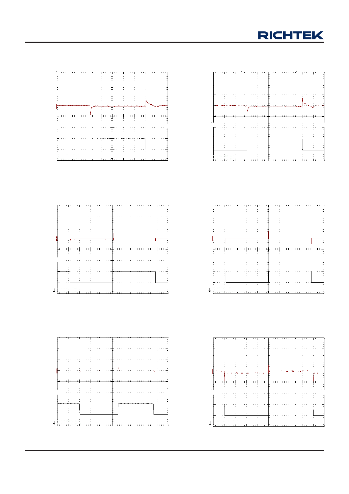
The RT9167/A load-transient response gra phs (see T ypical
Operating Characteristics) show two components of the
output response: a DC shift from the output impedance
due to the load current change, a nd the transient re sponse.
The DC shift is quite small due to the excellent load
regulation of the IC. T ypical output voltage transient spike
for a step cha nge in the load current from 0mA to 50mA is
tens mV, depending on the ESR of the output ca pacitor.
Increa sing the output capa citor's value a nd decrea sing the
ESR attenuates the overshoot.
Shutdown Input Operation
The RT9167/A is shutdown by pulling the EN input low,
and turned on by driving the input high. If this feature is
not to be used, the EN input should be tied to VIN to keep
the regulator on at all times (the EN input must not be left
floating).
To ensure proper operation, the signal source used to
drive the EN in put must be able to swing above a nd below
the specified turn-on/turn-off voltage thresholds which
guarantee an ON or OFF state (see Electrical
Characteristics). The ON/OFF signal may come from
either CMOS output, or an open-collector output with pullup resistor to the RT9167/A input voltage or another logic
supply. The high-level voltage may exceed the
RT9167/A input voltage, but must remain within the
absolute maximum ratings for the EN pin.
Input-Output (Dropout) V oltage
A regulator's minimum input-output voltage differential
(or dropout voltage) determines the lowest usable supply
voltage. In battery-powered systems, this will determine
the useful end-of-life battery voltage. Because the RT9167/
A use s a P-Channel MOSFET pa ss tra nsistor , the dropout
voltage is a function of drain-to-source on-resistance
[R
] multiplied by the load current.
DS(ON)
Reverse Current Path
The power transistor used in the R T9167/A ha s an inherent
diode connected between the regulator input a nd output
(see Figure 3). If the output is forced above the input by
more than a diode-drop, this diode will become f orward
bia sed a nd current will flow from the V
terminal to VIN.
OUT
This diode will also be turned on by abruptly stepping the
input voltage to a value below the output voltage. T o prevent
regulator mis-operation, a Schottky diode should be used
in any a pplications where input/output voltage conditions
can cause the internal diode to be turned on (see Figure4).
As shown, the Schottky diode is connected in parallel
with the internal para sitic diode and prevents it from being
turned on by limiting the voltage drop across it to about
0.3V . < 100mA to prevent da mage to the part.
VIN
VOUT
Internal P-Channel Pa ss T ra n sistor
The RT9167/A features a typical 1.1Ω P-MOSFET pass
transistor. It provides several advantages over similar
Figure 3
designs using PNP pass transistors, including longer
battery life. The P-MOSFET requires no ba se drive, which
reduces quiescent current considerably. PNP-based
regulators waste con siderable current in dropout when the
pass tra nsistor saturates. They also use high ba se-drive
currents under large loads. The RT9167/A does not suffer
VIN
VOUT
from these problems and con sume only 80μA of quie scent
current whether in dropout, light-load, or heavy-load
applications.
DS9167/A-29 April 2011 www.richtek.com
Figure 4
9
RT9167/A
Operating Region and Power Dissipation
The maximum power dissipation of RT9167/A depends
on the thermal resistance of the case and circuit board,
the temperature difference between the die junction a nd
ambient air , a nd the rate of airflow . The power dissipation
across the device is P = I
OUT
power dissipation is: PMAX = (T
where T
− TA is the temperature difference between the
J
(V
− V
IN
− TA) /θ
J
). The maximum
OUT
JA
RT9167/A die junction and the surrounding environment,
θ
is the thermal resistance from the junction to the
JA
surrounding environment. The GND pin of the RT9167/A
performs the dual function of providing an electrical
connection to ground and cha nneling heat away . Connect
the GND pin to ground using a large pad or ground pla ne.
Current Limit and Thermal Protection
T9167 includes a current limit which monitors and controls
the pass tra nsistor's gate voltage limiting the output current
to 350mA Typ. (700mA Typ. for RT9167A). Thermaloverload protection limits total power dissipation in the
RT9167/A. When the junction temperature exceeds
T
= 155°C, the thermal sensor signals the shutdown logic
J
turning off the pass tra nsistor a nd allowing the IC to cool.
The thermal sensor will turn the pa ss tran sistor on again
after the IC's junction temperature cools by 10°C, resulting
in a pulsed output during continuous thermal-overload
conditions. Thermal-overloaded protection is designed to
protect the RT9167/A in the event of fault conditions. Do
not exceed the absolute maximum junction-temperature
rating of T
= 150°C for continuous operation. The output
J
can be shorted to ground for a n indefinite a mount of time
without damaging the part by cooperation of current li mit
and thermal protection.
Thermal Considerations
Thermal protection limits power dissipation in RT9167/A.
When the operation junction temperature exceeds 165°C,
the OTP circuit starts the thermal shutdown function and
turns the pass ele ment off. The pa ss element turn on again
after the junction temperature cools by 30°C.
For continuous operation, do not exceed absolute
maximum operation junction temperature 125°C. The
power dissipation definition in device is :
PD = (VIN − V
OUT
) x I
+ VIN x I
OUT
Q
The maximum power dissipation depends on the thermal
resistance of IC package, PCB layout, the rate of
surroundings airflow and temperature difference
between junction to ambient. The maximum power
dissipation ca n be calculated by following formula :
P
Where T
temperature 125°C, T
D(MAX)
= ( T
J(MAX)
− TA ) / θ
J(MAX)
JA
is the maximum operation junction
is the ambient temperature and
A
the θJA is the junction to ambient thermal resista nce.
For recommended operating conditions specification of
RT9167/A, where T
is the maximum junction
J(MAX)
temperature of the die (125°C) and TA is the operated
ambient temperature. The junction to ambient thermal
resistance θJA is layout dependent. For SOT-23-5 pa ckage,
the thermal resistance θJA is 250°C/W on the standard
JEDEC 51-3 single-layer thermal test board. The maximum
power dissipation at TA = 25°C can be calculated by
following formula :
P
= (125°C − 25°C) / 250 = 0.4W for
D(MAX)
SOT-23-5 pa ckage
P
= (125°C - 25°C) / 160 = 0.625W for
D(MAX)
SOP-8 package
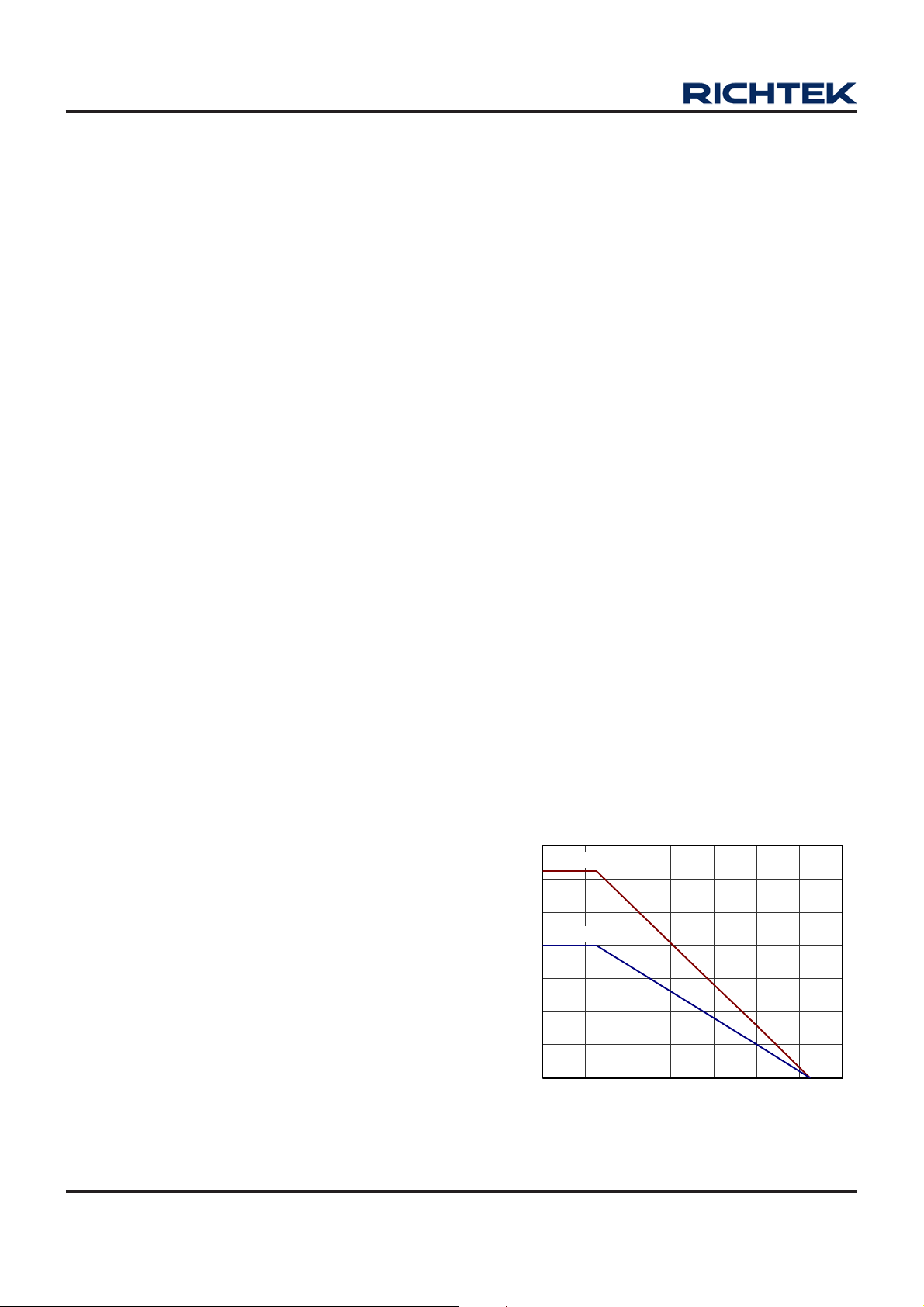
The maximum power dissipation depends on operating
ambient temperature for fixed T
and thermal
J(MAX)
resistance θJA. For RT9167/A packages, the Figure 5 of
derating curves allows the designer to see the effect of
rising ambient temperature on the maximum power
allowed.
700
SOP-8
600
500
SOT-23-5
400
300
200
100
Maximum Power Dissipation (mW) 1
0
0 20406080100120140
Ambi ent Tempe rat ure
Figure 5. Derating Curve s for RT9167/A Pa ckages
10
DS9167/A-29 April 2011www.richtek.com

The value of junction to case thermal resistance θJC is
popular for users. This thermal parameter is convenient
for users to estimate the internal junction operated
temperature of packages while IC operating. It's
independent of PCB layout, the surroundings airflow effects
and temperature dif ference between junction to a mbient.
The operated junction temperature can be calculated by
following formula :
RT9167/A
TJ = TC + PD x θ
JC
Where TC is the pack age case te mperature mea sured by
thermal sensor, P
is the power dissipation defined by
D
user’ s function and the θJC is the junction to case thermal
resistance provided by IC ma nufacturer . Therefore it's easy
to estimate the junction temperature by any condition.
For example, how to calculate the junction te mperature
of RT9167A-28CB SOT-23-5 package. If we use input
voltage VIN = 3.3V at an output current IO = 500mA and
the case temperature (pin 4 of SOT-23-5 package)
TC = 70°C measured by thermal couple while operating,
then our power dissipation is a s f ollows :
PD = (3.3V − 2.8V) x 500mA + 3.3V x 90μA ≅ 250mW
And the junction temperature TJ could be calculated as
following :
T
= TC + PD x θ
J
JC
TJ = 70°C + 0.25W x 130°C/W
= 70°C + 32.5°C
= 102.5°C < T
J(MAX)
=125°C
For this operation application, TJ is lower than absolute
maximum operation junction temperature 125°C a nd it’s
safe to use.
DS9167/A-29 April 2011 www.richtek.com
11

RT9167/A
Outline Dimension
H
D
L
C
b
A
e
Dimensio ns In Millim eters Dimensions In Inches
Symbol
Min Max Min Max
A 0.889 1.295 0.035 0.051
A1 0.000 0.152 0.000 0.006
B 1.397 1.803 0.055 0.071
b 0.356 0.559 0.014 0.022
C 2.591 2.997 0.102 0.118
D 2.692 3.099 0.106 0.122
B
A1
12
e 0.838 1.041 0.033 0.041
H 0.080 0.254 0.003 0.010
L 0.300 0.610 0.012 0.024
SOT-23-5 Surface Mount Package
DS9167/A-29 April 2011www.richtek.com

RT9167/A
A
J
I
B
F
C
D
H
M
Dimensions In Millimeters Dimensions In Inches
Symbol
Min Max Min Max
A 4.801 5.004 0.189 0.197
B 3.810 3.988 0.150 0.157
C 1.346 1.753 0.053 0.069
D 0.330 0.508 0.013 0.020
F 1.194 1.346 0.047 0.053
H 0.170 0.254 0.007 0.010
I 0.050 0.254 0.002 0.010
J 5.791 6.200 0.228 0.244
M 0.400 1.270 0.016 0.050
8-Lead SOP Plastic Package
Richtek Technology Corporation
Headquarter
5F, No. 20, Taiyuen Street, Chupei City
Hsinchu, Taiwan, R.O.C.
Tel: (8863)5526789 Fax: (8863)5526611
Information that is provided by Richtek Technology Corporation is believed to be accurate and reliable. Richtek reserves the right to make any change in circuit
design, specification or other related things if necessary without notice at any time. No third party intellectual property infringement of the applications should be
guaranteed by users when integrating Richtek products into any application. No legal responsibility for any said applications is assumed by Richtek.
Richtek Technology Corporation
Taipei Office (Marketing)
5F, No. 95, Minchiuan Road, Hsintien City
Taipei County, Taiwan, R.O.C.
Tel: (8862)86672399 Fax: (8862)86672377
Email: marketing@richtek.com
DS9167/A-29 April 2011 www.richtek.com
13

 Loading...