

DDR Termination Regulator
RT9026
General Description
RT9026 is a 3A sink/source tracking termination regulator .
It is specifically designed for low-cost and low-external
component count systems. The RT9026 possesses a high
speed operating amplif ier that provides fa st load transient
response and only requires 20μF of ceramic output
capacitance. The RT9026 supports remote sensing
functions and all features required to power the DDRI/II/III
and low-power DDRIII/DDRIV VTT bus termination
according to the JEDEC specification. In addition, the
RT9026 includes integrated sleep-state controls pla cing
VTT in High-Z in S3 (suspend to RAM) and soft-off f or VTT
and VTTREF in S5 (shutdown). The RT9026 is available
in the thermal efficient package SOP-8 (Exposed Pad),
MSOP-10 (Exposed Pad) and WDFN-10L 3x3.
Applications
z DDRI/II/III and Low-Power DDRIII/DDRIV Memory
Termination
z SSTL-2, SSTL-18
z HSTL T ermination
Ordering Information
RT9026
Package Type
SP : SOP-8 (Exposed Pad-Option 1)
FP : MSOP-10 (Exposed Pad)
QW : WDFN-10L 3x3 (W-Type)
Lead Plating System
P : Pb Free
G : Green (Halogen Free and Pb Free)
Note :
Richtek products are :
` RoHS compliant and compatible with the current require-
ments of IPC/JEDEC J-STD-020.
` Suitable for use in SnPb or Pb-free soldering processes.
Features
zz
Support DDRI, DDRII, DDRIII, Low-Power DDRIII and
z
zz
DDRIV Requirement
``
` Source/Sink 3A for DDRI and DDRII
``
``
` Source/Sink 2A for DDRIII
``
``
` Source/Sink 1.5A for Low-Power DDRIII
``
``
` Source/Sink 1.2A for Low-Power DDRIV
``
zz
z Input Voltage Range : 3.15V to 5.5V
zz
zz
z VLDOIN Voltage Range : 1.2V to 3.3V
zz
zz
z Requires Only 20
zz
zz
z Supports High-Z in S3 and Soft-Off in S5
zz
zz
z Integrated Divider T racks 1/2 V DDQSNS for Both VTT
zz
μμ
μF Ceramic Output Capacitance
μμ
and VTTREF
zz
z Remote Sensing (VTTSNS)
zz
zz
z ±20mV Accuracy for VTT and VTTREF
zz
zz
z 10mA Buffered Reference (Sourcing/Sinking)
zz
(VTTREF)
zz
z Built-In Soft-Start
zz
zz
z Over Current Protection
zz
zz
z Thermal Shutdown Protection
zz
zz
z SOP-8 (Exposed Pad), MSOP-10 (Exposed Pad) and
zz
10-Lead WDFN Package
zz
z RoHS Compliant and Halogen Free
zz
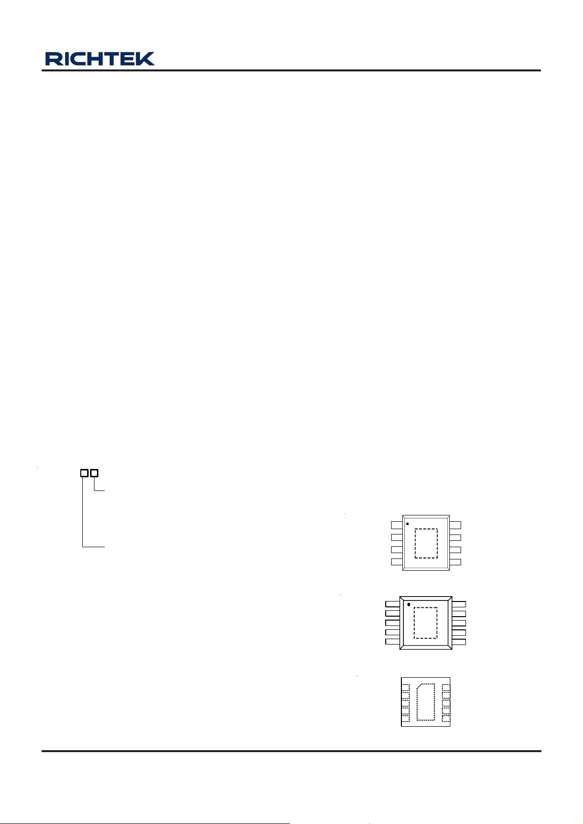
Pin Configurations
(TOP VIEW)
GND
GND
8
VTT
7
VLDOIN
6
5
10
9
8
7
6
VIN
VDDQSNS
VIN
S5
GND
S3
VTTREF
9
11
GND
2
S3
VTTSNS
VTTREF
3
4
SOP-8 (Exposed Pad)
VDDQSNS
VLDOIN
VTT
PGND
VTTSNS
2
3
4
5
MSOP-10 (Exposed Pad)
VDDQSNS
VLDOIN
VTT
PGND
VTTSNS
1
2
3
4
5
GND
10
VIN
9
S5
8
GND
7
S3
9
11
VTTREF
WDFN-10L 3x3
DS9026-06 August 2011 www.richtek.com
1
RT9026
Marking Information
RT9026PSP
RT9026PSP : Product Code
RT9026
PSPYMDNN
YMDNN : Date Code
RT9026PFP
A0-YM
DNN
A0- : Product Code
YMDNN : Date Code
RT9026GSP
RT9026GSP : Product Code
RT9026
YMDNN : Date Code
GSPYMDNN
RT9026PQW
E6- : Product Code
E6-YM
YMDNN : Date Code
DNN
RT9026GQW
E6= : Product Code
E6=YM
YMDNN : Date Code
DNN
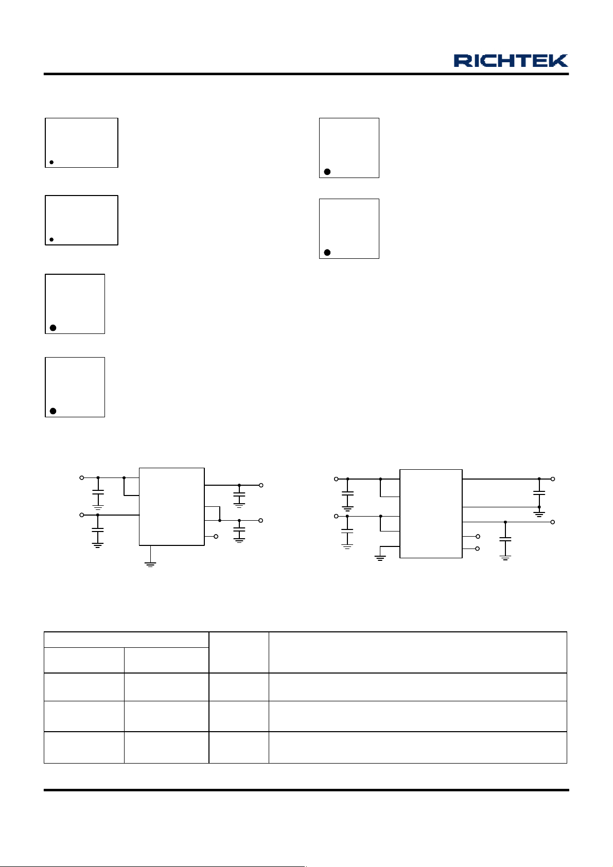
Typical Application Circuit
RT9026
VLDOIN
3.3V or 5V
C1
10µF
C2
1µF
7
VLDOIN
5
6
VTTREF
VDDQSNS
VTTSNS
VIN
GND
1, 9 (Exposed Pad)
VTT
S3
4
3
8
2
S3
VTTREF
C3
0.1µF
VTT
C4
10µF x 2
RT9026GFP
A0=YM
DNN
VLDOIN
C1
10µF
VTT
C4
10µF x 2
A0= : Product Code
YMDNN : Date Code
RT9026
1
VDDQSNS
2
VLDOIN
3
VTT
5
VTTSNS
4
PGND
VIN
GND
VTTREF
S5
S3
10
8, 11 (Exposed Pad)
6
9
S5
7
S3
C3
0.1µF
3.3V or 5V
C2
1µF
VTTREF
Figure 1. For SOP-8 (Exposed Pad) Package Figure 2. For MSOP-10 (Exposed Pad) / WDFN-10L 3x3
Package
Functional Pin Description
Pin No.
RT9026□SP
1,
9 (Exposed Pad)
2 7 S3
3 5 VTTSNS
RT9026□FP
RT9026□QW
8,
11 (Exposed Pad)
Pin Name
GND
Ground. The exposed pad must be soldered to a large PCB and
connected to GND for maximum power dissipation.
Active Low Suspend to RAM Mode Control Pin, VTT is turned
off and left High-Z, VTTREF is active.
VTT Voltage Sense Input Pin. Connect to plus terminal of the
output capacitor.
2
Pin Function
To be Continued
DS9026-06 August 2011www.richtek.com
Pin No.
RT9026□SP
RT9026□FP
RT9026□QW
4 6 VTTREF
Pin Name
Buffered output that is a reference output, equal to
VDDQSNS/2.
5 1 VDDQSNS VLDOIN Sense Input Pin.
6 10 VIN Analog Input Pin (to control loop).
7 2 VLDOIN
8 3 VTT
Power supply of the VTT and VTTREF output stage (to power
MOS).
Output voltage for connection to termination resistors, equal to
VDDQSNS/2.
-- 4 PGND Power Ground of the VTT Output.
RT9026
Pin Function
-- 9 S5
Function Block Diagram
VDDQSNS
GND
VIN
+
VIN OK
-
S3
S5
2.32V/
2.2V
ENREF
Half DDQ
+
-
ENVTT
Active low shutdown control pin, both VTT and VTTREF are
turned off and discharged to ground.
VLDOIN
+
-
+
-
5V(10%)
+
+
-5V(10%)
ENREF
ENVTT
+
-
+
-
PGOOD
VTTREF
VTT
PGND
VTTSNS
Table 1. S3 and S5 Control Table
State S3 S5 VTT VREF
Normal High High
Standby Low High
Shutdown
Shutdown
DS9026-06 August 2011 www.richtek.com
Low Low 0V (Discharge) 0V (Discharge)
High Low 0V (Discharge) 0V (Discharge)
1.25V/0.9V/0.75V
/0.675V/0.6V
12mV/6mV
(High-Z)
1.25V/0.9V/0.75V
/0.675V/0.6V
1.25V/0.9V/0.75V
/0.675V/0.6V
3
RT9026
Supply
Absolute Maximum Ratings (Note 1)
l Supply Input Voltage, VIN----------------------------------------------------------------------------------------------6V
l Supply Input Voltage, VLDOIN, VDDQSNS------------------------------------------------------------------------3.6V
l Power Dissipation, P
SOP-8 (Exposed Pad)--------------------------------------------------------------------------------------------------1.333W
MSOP-10 (Exposed Pad)----------------------------------------------------------------------------------------------1.163W
WDFN-10L 3x3-----------------------------------------------------------------------------------------------------------1.429W
l Package Thermal Resistance (Note 2)
SOP-8 (Exposed Pad), θJA--------------------------------------------------------------------------------------------75°C/W
SOP-8 (Exposed Pad), θJC--------------------------------------------------------------------------------------------28°C/W
MSOP-10 (Exposed Pad), θJA----------------------------------------------------------------------------------------86°C/W
MSOP-10 (Exposed Pad), θJC----------------------------------------------------------------------------------------30°C/W
WDFN-10L 3x3, θJA------------------------------------------------------------------------------------------------------70°C/W
WDFN-10L 3x3, θJC-----------------------------------------------------------------------------------------------------8.2°C/W
l Lead Temperature (Soldering, 10 sec.)------------------------------------------------------------------------------260°C
l Junction Temperature---------------------------------------------------------------------------------------------------150°C
l Storage Temperature Range------------------------------------------------------------------------------------------- −65°C to 150°C
l ESD Susceptibility (Note 3)
HBM (Human Body Mode)---------------------------------------------------------------------------------------------2kV
MM (Machine Mode)----------------------------------------------------------------------------------------------------200V
@ TA = 25°C
D
Recommended Operating Conditions (Note 4)
l Supply Input Voltage, VIN----------------------------------------------------------------------------------------------3.15V to 5.5V
l Supply Input Voltage, VLDOIN, VDDQSNS------------------------------------------------------------------------1.2V to 3.3V
l Junction Temperature Range------------------------------------------------------------------------------------------ −40°C to 125°C
l Ambient Temperature Range------------------------------------------------------------------------------------------ −40°C to 85°C
Electrical Characteristics
(VIN = 5V, VLDOIN = VDDQSNS = 2.5V, C1=10µF, C2=1µF, C3=0.1µF, C4=10µFx2, T
and RT9026PQW, unless otherwise specified)
Parameter Symbol Test Conditions Min Typ Max Unit
VIN (to control loop)
Current
VIN Standby Current I
VIN Shutdown Current I
VLDOIN (to power MOS)
Supply Current
VLDOIN Standby Current I
VLDOIN Shutdown Current I
VDDQSNS Input Current I
VTTSNS Input Current I
I
VIN = 5V, No Load, S5 = S3 = 5V -- -- 2 mA
VIN
VIN = 5V, No Load, S5 = 5V, S3 = 0V -- -- 300 µA
VINSTB
VIN = 5V, No Load, S5 = S3 = 0V
VINSHDN
I
VLDOIN
VLDOINSTB
VLDOINSHDN
VDDQSNS
VTTSNS
(Only for RT9026PFP and RT9026PQW)
VIN = 5V, No Load, S5 = S3 = 5V -- -- 2 mA
VIN = 5V, No Load, S5 = 5V, S3 = 0V -- -- 10 µA
VIN = 5V, No Load, S5 = S3 = 0V -- -- 1 µA
VIN = 5V, S5 = S3 = 5V -- -- 50 µA
VIN = 5V, S5 = S3 = 5V -- -- 1 µA
VDDQSNS = VLDOIN = 2.5V -- 1.25
VTT Output Voltage VTT
VDDQSNS = VLDOIN = 1.8V -- 0.9 -VDDQSNS = VLDOIN = 1.5V -- 0.75
= 25°C, S5 function only for RT9026PFP
A
-- -- 1 µA
--
--
V
To be Continued
DS9026-06 August 2011www.richtek.com
4
Parameter Symbol Test Conditions Min Typ Max Unit
= 2.5V/1.8V,
VTT Output Voltage VTT
VTTREF, VTT Output
Tolerance
VTT Source Current Limit I
V
VTTTOL
VTTOCLsr
RT9026
VDDQSNS = VLDOIN = 1.35V -- 0.675
VDDQSNS = VLDOIN = 1.2V -- 0.6 -VDDQSNS = VLDOIN =
2.5V/1.8V/1.5V/1.35V/1.2V,
∣I
∣= 0A
VTT
VDDQSNS = VLDOIN = 1.2V,
∣I
∣= 1.2A
VTT
−20
−30
-- 20
-- 30
VDDQSNS = VLDOIN =
2.5V/1.8V/1.5V/1.35V,
∣I
∣= 1.5A
VTT
VDDQSNS = VLDOIN
∣I
∣= 3A
VTT
−30
−40
-- 30
-- 40
VTT = 0V 3 4 -- A
-V
mV
VTT Sink Current Limit I
VTT Discharge Current I
VTTREF Output Voltage V
VDDQSNS/2, VTTREF
Output Voltage Tolerance
VTTREF Source Current Limit I
VTTOCLsk
DSCHRG
VTTREF
V
VTTREFTOL
VTTREFOCL
VTT = VDDQSNS 3 4 -- A
VDDQSNS = 0V, VTT = 1.25V,
S5 = S3 = 0V
V
VTTREF
V2
VDDQSNS
=
--
10 17 -- mA
1.25/0.9/
0.75/
-- V
0.675/0.6
VLDOIN = VDDQSNS =
2.5V/1.8V/1.5V/1.35V/1.2V,
I
VTTREF
V
VTTREF
< 10mA
= 0V 20 40 60 mA
−20 -- 20 mV
Rising -- -- 2.7
UVLO Threshold Voltage V
UVLO
V
Hysteresis -- 0.2 --
Logic-High VIH S5, S3 pin 1.6 -- --
Input Voltage
V
Logic-Low VIL S5, S3 pin -- -- 0.4
Logic Input Leakage Current I
S5, S3 pin -- -- 1 µA
ILK
Thermal Shutdown Protection TSD -- 160 -- °C
Thermal Shutdown Hysteresis ∆TSD -- 20 -- °C
Note 1. Stresses listed as the above “ Absolute Maximum Ratings” may cause permanent damage to the device. These are for
stress ratings. Functional operation of the device at these or any other conditions beyond those indicated in the
operational sections of the specifications is not implied. Exposure to absolute maximum rating conditions for extended
periods may remain possibility to affect device reliability.
Note 2. θJA is measured in the natural convection at TA = 25°C on a high effective four-layers thermal conductivity test board of
JEDEC 51-7 thermal measurement standard. The case point of θJC is on the exposed pad for SOP-8 (Exposed Pad)
, MSOP-10 (Exposed Pad) and WDFN-10L 3x3 package.
Note 3. Devices are ESD sensitive. Handling precaution is recommended.
Note 4. The device is not guaranteed to function outside its operating conditions.
DS9026-06 August 2011 www.richtek.com
5
RT9026
)
Typical Operating Characteristics
V
DDQSNS
= V
, C1 = 10μF, C2 = 1μF, C3 = 0.1μF, C4 = 10μF x 2 unless otherwise specified.
LDOIN
1.25VTT Output Voltage vs. Temperature
1.30
1.28
1.26
1.24
Output Voltage (V )
1.22
V
= 2.5V
1.20
LDOIN
-50 -25 0 25 50 75 100 125
Temperature (°C)
0.75VTT Output Voltage vs. Temperature
0.80
0.79
0.78
0.77
0.76
0.75
0.74
0.73
Output Voltage (V )
0.72
0.71
V
= 1.5V
0.70
LDOIN
-50 -25 0 25 50 75 100 125
Temperature (°C)
VIN = 3.3V
VIN = 5V
VIN = 3.3V
VIN = 5V
0.9VTT Output Voltage vs. Temperature
0.95
0.94
0.93
0.92
0.91
0.90
0.89
0.88
Output Voltage ( V)
0.87
0.86
V
= 1.8V
0.85
LDOIN
-50 -25 0 25 50 75 100 125
VIN = 3.3V
Temperatu re (°C)
0.675VTT Output Voltage vs. Temperature
0.725
0.715
0.705
0.695
0.685
0.675
0.665
0.655
Output Voltage ( V )
0.645
0.635
V
= 1.35V
0.625
LDOIN
-50-25 0 25 50 75100125
Temperature (°C)
VIN = 3.3V
VIN = 5V
VIN = 5V
0.6VTT Output Voltage vs. Temperature
0.65
0.64
0.63
0.62
0.61
0.60
0.59
0.58
Output Voltage (V)
0.57
0.56
V
= 1.2V
0.55
LDOIN
-50-25 0 25 50 75100125
Temperatu re (°C)
VIN = 3.3V
VIN = 5V
1000
Supply Current (µA
IN
V
VIN Supply Current vs. Temperature
VIN = 5V, V
950
900
850
800
750
700
650
600
-50-25 0 25 50 75100125
= 2.5V
LDOIN
V
= 1.8V
LDOIN
Temperature (°C)
VIN = 5V, V
VIN = 3.3V, V
V
V
V
V
V
V
LDOIN
LDOIN
LDOIN
LDOIN
LDOIN
LDOIN
LDOIN
LDOIN
= 1.5V
= 1.35V
= 1.2V
= 2.5V
= 1.8V
= 1.5V
= 1.35V
= 1.2V
DS9026-06 August 2011www.richtek.com
6
RT9026
)
250
230
210
190
Standby Current (µA
IN
170
V
150
V
TT
(20mV/Div)
VIN Standby Current vs. Te m pe rature
VIN = 5V, V
-50-250 255075100125
= 2.5V
LDOIN
V
= 1.8V
LDOIN
V
= 1.5V
LDOIN
V
= 1.35V
LDOIN
V
= 1.2V
LDOIN
Temperature (°C)
VIN = 3.3V, V
V
V
V
V
LDOIN
LDOIN
LDOIN
LDOIN
LDOIN
= 2.5V
= 1.8V
= 1.5V
= 1.35V
= 1.2V
0.9VTT @ 3A Transient Response
VIN = 5V, V
LDOIN
= 1.8V
Source
V
TT
(20mV/Div)
I
VTT
(2A/Div)
V
TT
(20mV/Div)
1.25VTT @ 3A Transient Response
VIN = 5V, V
= 2.5V
LDOIN
Time (500μs/Div)
0.75VTT @ 2A Transient Response
VIN = 5V, V
LDOIN
= 1.5V
Source
Source
I
VTT
(2A/Div)
V
TT
(20mV/Div)
I
VTT
(1A/Div)
Time (500μs/Div)
0.675VTT @ 1.5A Transient Response
VIN = 5V, V
LDOIN
= 1.35V
Source
I
VTT
(1A/Div)
V
TT
(20mV/Div)
I
VTT
(1A/Div)
Time (500μs/Div)
0.6VTT @ 1.2A Transient Response
VIN = 5V, V
LDOIN
= 1.2V
Source
Time (400μs/Div) Time (400μs/Div)
DS9026-06 August 2011 www.richtek.com
7

RT9026
V
TT
(20mV/Div)
I
VTT
(2A/Div)
V
TT
(20mV/Div)
1.25VTT @ 3A Transient Response
VIN = 5V, V
= 2.5V
LDOIN
Time (500μs/Div)
0.75VTT @ 2A Transient Response
VIN = 5V, V
LDOIN
= 1.5V
Sink
Sink
V
TT
(20mV/Div)
I
VTT
(2A/Div)
V
TT
(20mV/Div)
0.9VTT @ 3A Transient Response
VIN = 5V, V
= 1.8V
LDOIN
Time (500μs/Div)
Sink
0.675VTT @ 1.5A Transient Response
VIN = 5V, V
LDOIN
= 1.35V
Sink
I
VTT
(1A/Div)
V
TT
(20mV/Div)
I
VTT
(1A/Div)
0.6V
TTREF
VIN = 5V, V
Time (500μs/Div)
@ 1.2A Transient Response
= 1.2V
LDOIN
Time (400μs/Div)
Sink
I
VTT
(1A/Div)
V
TTREF
(10mV/Div)
I
VTTREF
(10mA/Div)
0.9V
TTREF
VIN = 5V, V
Time (400μs/Div)
@ 10mA Transient Response
= 1.8V
LDOIN
Time (1ms/Div)
Source
DS9026-06 August 2011www.richtek.com
8
RT9026
V
TTREF
(10mV/Div)
I
VTTREF
(10mA/Div)
S3
(5V/Div)
S5
(5V/Div)
V
TTREF
(1V/Div)
V
TT
(1V/Div)
0.9V
VIN = 5V, V
@ 10mA Transient Response
TTREF
= 1.8V
LDOIN
Time (1ms/Div)
Start Up
S3 = 0V, C3 = 1μF, S5 : Low to High
Sink
S3
(5V/Div)
S5
(5V/Div)
V
TTREF
(1V/Div)
V
TT
(1V/Div)
S3
(5V/Div)
S5
(5V/Div)
V
TTREF
(1V/Div)
V
TT
(1V/Div)
Start Up
S3 = 0V, C3 = 0.1μF, S5 : Low to High
Time (2.5μs/Div)
Start Up
S3 = 0V, S5 = 5V, S3 : Low to High
Time (10μs/Div)
Time (10μs/Div)
Power Off
S3
S3
(5V/Div)
S5
S5
(5V/Div)
V
TTREF
(1V/Div)
V
(1V/Div)
DS9026-06 August 2011 www.richtek.com
V
TTREF
V
TT
TT
S3 = 0V, C3 = 0.1μF, S3 and S5 : High to Low
Time (1ms/Div)
9

RT9026
(
(
Application Information
RT9026 is a 3A sink/source tracking termination regulator .
It is specifically designed for low-cost and low-external
component count system such as notebook PC
applications. The RT9026 possesses a high speed
operating amplifier that provides fa st load tra nsient response
and only requires a 10μF cera mic input ca pacitor a nd two
10μF ceramic output ca pa citor .
VTTREF Regulator
VTTREF is a reference output voltage with source/sink
current capa bility up to 10mA. T o en sure stable operation
0.1μF ceramic capacitor between VTTREF and GND is
recommended.
S3, S5 Logic Control
The S3 and S5 terminals should be connected to SLP_S3
and SLP_S5 signals respectively . Both VTTREF a nd VTT
are turned on at normal state (S3 = High, S5 = High). In
standby state (S3 = Low, S5 = High) VTTREF is kept
alive while VTT is turned off a nd left high impedance. Both
VTT and VTTREF outputs are turned of f and discharged
to ground through internal MOSFETs during shutdown
state (S5 = low).
Table 2. S3 and S5 Control
STATE S3 S5 VTTREF VTT
Normal H H ON ON
Standby L H ON OFF(high-Z)
Shutdown L L
OFF
discharge)
OFF
discharge)
For stable operation, the total ca pacita nce of the cerarnic
capcitor at the VTT output terminal must not be larger
than 30μF. The RT9026 is designed specifically to work
with low ESR ceramic output capacitor in space saving
and performa nce consideration. Larger output ca pacita nce
can reduce the noise a nd improve load tran sient response,
stability and PSRR. The output capa citor should be located
near the VTT output terminal pin as close as possible.
Thermal Considerations
For continuous operation, do not exceed absolute
maximum operation junction temperature. The maximum
power dissipation depends on the thermal resistance of
IC package, PCB layout, the rate of surroundings airflow
and temperature difference between junction to a mbient.
The maximum power dissipation can be calculated by
following formula :
P
Where T
temperature, T
D(MAX)
= ( T
J(MAX)
− TA ) / θ
J(MAX)
JA
is the maximum operation junction
is the ambient temperature a nd the θ
A
JA
the junction to ambient thermal resistance.
For recommended operating conditions specification of
the RT9026, the maximum junction temperature is 125°C.
The junction to ambient thermal resistance θJA is layout
dependent. The thermal resista nce θJA for W DF N-10L 3x3
is 70°C/W, for SOP-8 (Exposed Pad) is 75°C/W and for
MSOP-10 (Exposed Pad) is 86°C/W on the standard
JEDEC 51-7 four layers thermal test board. The maximum
power dissipation at T
= 25°C can be calculated by
A
following formula :
is
Capacitor Selection
P
= (125°C − 25°C) / (70°C/W) = 1.429W for
D(MAX)
W DF N-10L 3x3 pa ckages
Good bypassing is recommended from VLDOIN to GND
to help improve AC performance. A 10μF or greater input
capacitor located as close as possible to the IC is
recommended. The input ca p a citor must be located at a
distance of less than 0.5 inches from the VLDOIN pin of
the IC.
Adding a ceramic capacitor 1μF close to the VIN pin a nd
it should be kept away from any para sitic impeda nce from
the supply power.
P
SOP-8 (Exposed Pad) packages
P
MSOP-10 (Exposed Pad) packages
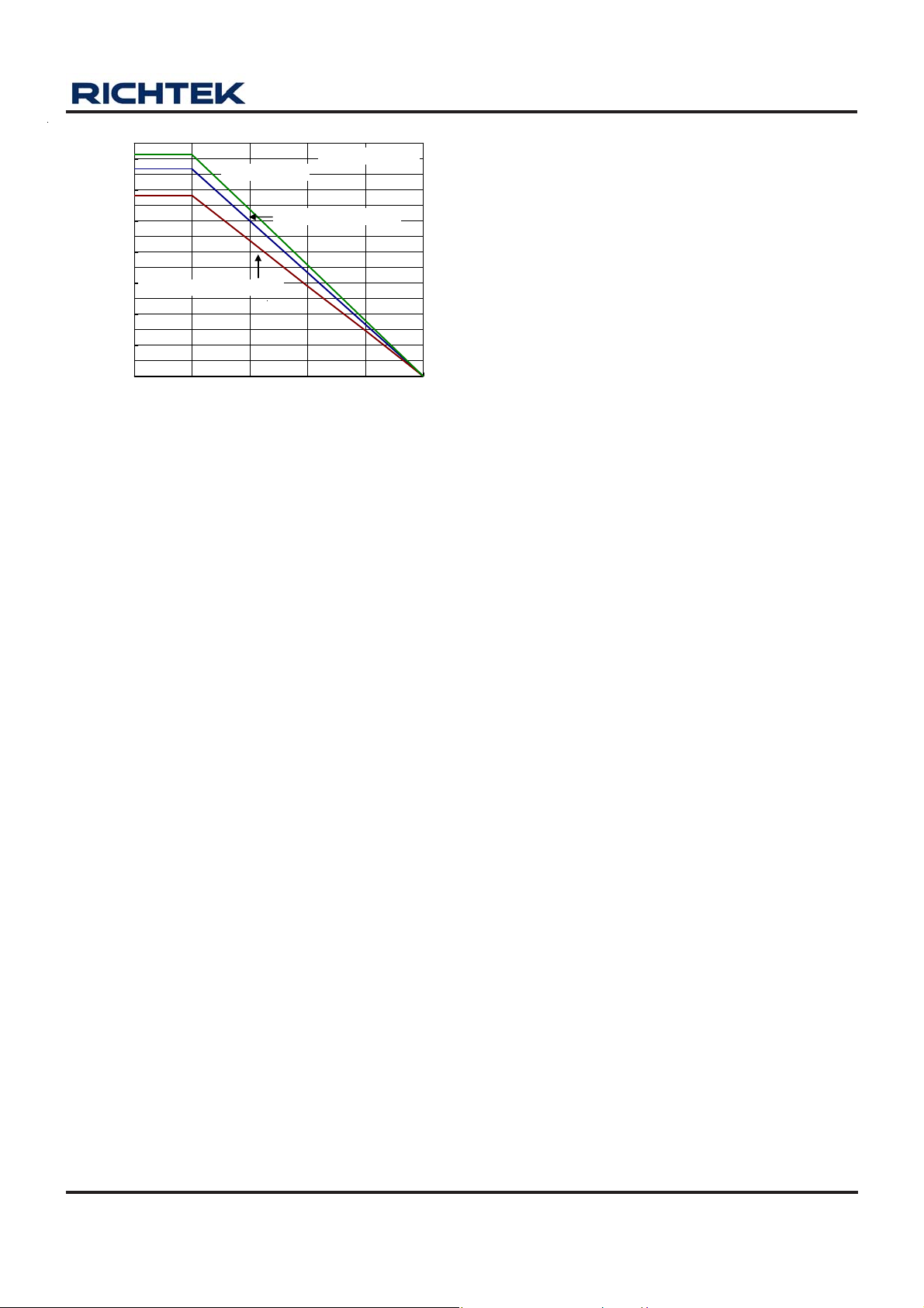
The maximum power dissipation depends on operating
ambient temperature for fixed T
resistance θJA. For RT9026 packages, the Figure 3 of
derating curves allows the designer to see the effect of
= (125°C − 25°C) / (75°C/W) = 1.333W for
D(MAX)
= (125°C − 25°C) / (86°C/W) = 1.163W for
D(MAX)
and thermal
J(MAX)
rising ambient temperature on the maximum power
allowed.
DS9026-06 August 2011www.richtek.com
10
RT9026
1.5
1.4
1.3
1.2
1.1
1.0
0.9
0.8
0.7
0.6
MSOP-10 (Exposed Pad)
0.5
0.4
0.3
0.2
0.1
Maximum Power Dissipation (W) 1
0.0
0 25 50 75 100 125
WDFN-10L 3x3
Four-Layers PCB
SOP-8 (Exposed Pad)
Ambient Temperature (°C)
Figure 3. Derating Curves f or the RT9026 Pack ages
DS9026-06 August 2011 www.richtek.com
11

RT9026
Outline Dimension
A
EXPOSED THERMAL PAD
(Bottom of Package)
J
I
Dimensions In Millimeters Dimensions In Inches
Symbol
Min Max Min Max
A 4.801 5.004 0.189 0.197
B 3.810 4.000 0.150 0.157
Y
B
X
F
C
D
H
M
C 1.346 1.753 0.053 0.069
D 0.330 0.510 0.013 0.020
F 1.194 1.346 0.047 0.053
H 0.170 0.254 0.007 0.010
M 0.406 1.270 0.016 0.050
Option 1
Option 2
I 0.000 0.152 0.000 0.006
J 5.791 6.200 0.228 0.244
X 2.000 2.300 0.079 0.091
Y 2.000 2.300 0.079 0.091
X 2.100 2.500 0.083 0.098
Y 3.000 3.500 0.118 0.138
8-Lead SOP (Exposed Pad) Plastic Package
12
DS9026-06 August 2011www.richtek.com

RT9026
D
L
EXPOSED THERMAL PAD
(Bottom of Package)
Dimensions In Millimeters Dimensions In Inches
Symbol
A 0.810 1.100 0.032 0.043
A1 0.000 0.100 0.000 0.004
A2 0.750 0.950 0.030 0.037
E
A
Min Max Min Max
U
E1
V
e
A2
A1
b
b 0.170 0.270 0.007 0.011
D 2.900 3.100 0.114 0.122
e 0.500 0.020
E 4.800 5.000 0.189 0.197
E1 2.900 3.100 0.114 0.122
L 0.400 0.800
U 1.300 1.700
V 1.500 1.900
10-Lead MSOP (Exposed Pad) Plastic Package
0.016 0.031
0.051 0.067
0.059 0.075
DS9026-06 August 2011 www.richtek.com
13

RT9026
D
E
A
A3
A1
D2
L
E2
SEE DETAIL A
1
2
e
b
1
1
2
DETAIL A
Pin #1 ID a nd T ie Bar Mark Option s
Note : The configuration of the Pin #1 identifier is optional,
but must be located within the zone indicated.
Dimensions In Millimeters Dimensions In Inches
Symbol
Min Max Min Max
A 0.700 0.800 0.028 0.031
A1 0.000 0.050 0.000 0.002
A3 0.175 0.250 0.007 0.010
b 0.180 0.300 0.007 0.012
D 2.950 3.050 0.116 0.120
D2 2.300 2.650 0.091 0.104
E 2.950 3.050 0.116 0.120
E2 1.500 1.750 0.059 0.069
e 0.500 0.020
L 0.350 0.450
Richtek Technology Corporation
Headquarter
5F, No. 20, Taiyuen Street, Chupei City
Hsinchu, Taiwan, R.O.C.
Tel: (8863)5526789 Fax: (8863)5526611
0.014 0.018
W-Type 10L DFN 3x3 Package
Richtek Technology Corporation
Taipei Office (Marketing)
5F, No. 95, Minchiuan Road, Hsintien City
Taipei County, Taiwan, R.O.C.
Tel: (8862)86672399 Fax: (8862)86672377
Email: marketing@richtek.com
Information that is provided by Richtek Technology Corporation is believed to be accurate and reliable. Richtek reserves the right to make any change in circuit
design, specification or other related things if necessary without notice at any time. No third party intellectual property infringement of the applications should be
guaranteed by users when integrating Richtek products into any application. No legal responsibility for any said applications is assumed by Richtek.
DS9026-06 August 2011www.richtek.com
14

 Loading...