

Datasheet RT9018A-10GQW, RT9018A-12GQW, RT9018A-12PQW, RT9018A-15GQW, RT9018A-18GQW Datasheet (Richtek) [ru]
...Page 1
®
Maximum 3A, Ultra Low Dropout Regulator
RT9018A/B
General Description
The RT9018A/B is a high performance positive voltage
regulator designed for use in applications requiring very
low Input voltage and very low dropout voltage at up to
3A(Peak). It operates with a VIN as low as 1.4V and VDD
voltage 3V with output voltage programmable as low as
0.8V. The significant feature includes ultra low dropout,
ideal for applications where VOUT is very close to VIN.
Additionally, there is an enable pin to further reduce power
dissipation while shutdown. The RT9018A/B provides
excellent regulation over variations in line, load and
temperature. and provides a power OK signal to indicate
if the voltage level of Vo reaches 90% of its rating value.
The RT9018A/B is available in the SOP-8 (Exposed Pad)
and WDFN-10L 3x3 packages with 1V, 1.05V, 1.2V, 1.5V,
1.8V and 2.5V internally preset outputs that are also
adjustable using external resistors.
Ordering Information
RT9018A/B-
Package Type
SP : SOP-8 (Exposed Pad-Option 1)
QW : WDFN-10L 3x3
Lead Plating System
P : Pb Free
G : Green (Halogen Free and Pb Free)
Z : ECO (Ecological Element with
Halogen Free and Pb free)
Output Voltage
10 : 1V/Adj
1K : 1.05V/Adj
12 : 1.2V/Adj
15 : 1.5V/Adj
18 : 1.8V/Adj
25 : 2.5V/Adj
Enable Pin Function
A : Internal Pull High
B : Internal Pull Low
Note :
Richtek products are :
` RoHS compliant and compatible with the current require-
ments of IPC/JEDEC J-STD-020.
` Suitable for use in SnPb or Pb-free soldering processes.
Features
zz
z Maximum 3A Low-Dropout Voltage Regulator
zz
zz
z High Accuracy Output Voltage
zz
zz
z Typically 210mV Dropout at 3A
zz
zz
z Power Good Output
zz
zz
z Output Voltage Pull Low Resistance when Disable
zz
zz
z Thermal and Over Current Protection
zz
zz
z RoHS Compliant and 100% Lead (Pb)-Free
zz
±±
±1.5%
±±
Applications
z Front Side Bus VTT (1.2V/3A)
z NoteBook PC Applications
z Motherboard Applications
Marking Information
For marking information, contact our sales representative
directly or through a Richtek distributor located in your
area.
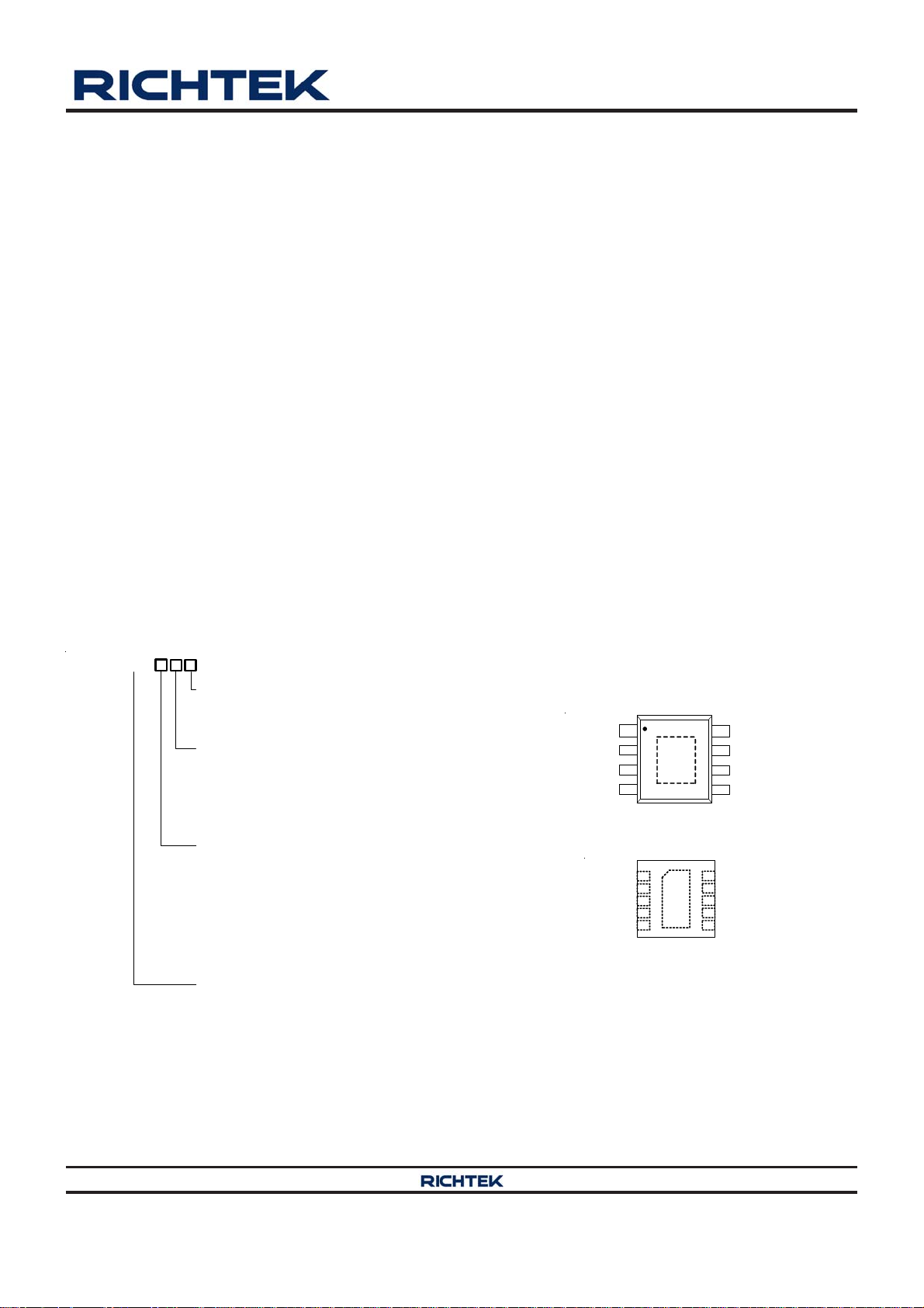
Pin Configurations
(TOP VIEW)
GND
GND
8
GND
7
ADJ
6
9
11
VOUT
5
NC
VDD
10
9
VIN
8
VIN
7
VIN
9
EN
PGOOD
EN
VIN
VDD
2
3
4
SOP-8 (Exposed Pad)
1
VOUT
2
VOUT
3
VOUT
4
ADJ
PGOOD
5
WDFN-10L 3x3
Copyright 2012 Richtek Technology Corporation. All rights reserved. is a registered trademark of Richtek Technology Corporation.
©
DS9018A/B-09 April 2012 www.richtek.com
1
Page 2
RT9018A/B
Typical Application Circuit
10µF
VIN
EN
VDD
1µF
VOUT
RT9018A/B
PGOOD
GND
ADJ
V
100k
OUT
V
IN
Chip Enable
V
DD
Figure 1. Fixed Voltage Regulator Figure 2. Adjustable Voltage Regulator
10µF
V
OUT
V
IN
Chip Enable
R2R1
×=
R1
R2
+
R2
10µF
V
OUT
0.8 V
OUT
VIN
10µF
EN
V
DD
VDD
1µF
VOUT
RT9018A/B
PGOOD
GND
ADJ
C
Dummy
100k
V
OUT
Function
Pin Description
Pi n No.
SOP-8
(Exposed Pad)
WDFN -1 0L 3x3
3 7, 8, 9 VIN Supply Input Voltage.
2 6 EN Chip Enable (Active-High).
4 10 VDD Supply Voltage of Control Circuitry.
1 5 PGOOD Power Good Open Drain Output.
7 4 ADJ
6 1, 2, 3 VOUT Output Voltage.
5 -- NC No Internal Connection.
8,
9 (Exposed Pad)
11 (Exposed Pad) GND
Function Block Diagram
VIN
Pin
Name
Pin Function
Set the output voltage by the internal feedback resistors when
ADJ is grounded. If external feedback resistors is used, V
OUT
=
0.8V x (R 1 + R2) /R2.
Ground. The exposed pad must be soldered to a large PCB
and connected to GND for maximum power dissipation.
VOUT
OCP
OTP
EN
VDD
Copyright 2012 Richtek Technology Corporation. All rights reserved. is a registered trademark of Richtek Technology Corporation.
©
POR
Driver
0.8V
0.72V
+
Error
Amplifier
-
+
Mode
ADJ
PGOOD
GND
DS9018A/B-09 April 2012www.richtek.com
2
Page 3
RT9018A/B
Absolute Maximum Ratings (Note 1)
z Supply Voltage, VIN ------------------------------------------------------------------------------------------------------ 1V to 6V
z Control Voltage, VDD ----------------------------------------------------------------------------------------------------- 3V to 6V
z Output Voltage, VOUT --------------------------------------------------------------------------------------------------- 0.8 to 6V
z Power Dissipation, P
SOP-8 (Exposed Pad) --------------------------------------------------------------------------------------------------- 1.33W
WDFN-10L 3x3 ------------------------------------------------------------------------------------------------------------- 1.67W
z Package Thermal Resistance (Note 2)
SOP-8 (Exposed Pad), θJA---------------------------------------------------------------------------------------------- 75°C/W
SOP-8 (Exposed Pad), θJC--------------------------------------------------------------------------------------------- 15°C/W
WDFN-10L 3x3, θJA------------------------------------------------------------------------------------------------------- 60°C/W
z Junction Temperature ----------------------------------------------------------------------------------------------------- 150°C
z Lead Temperature (Soldering, 10 sec.)------------------------------------------------------------------------------- 260°C
z Storage Temperature Range -------------------------------------------------------------------------------------------- −65°C to 150°C
z ESD Susceptibility (Note 3)
HBM (Human Body Mode) ---------------------------------------------------------------------------------------------- 2kV
MM (Machine Mode) ------------------------------------------------------------------------------------------------------ 200V
@ TA = 25°C
D
Recommended Operating Conditions (Note 4)
z Supply Voltage, V
z Control Voltage, VDD
z Control Voltage with PGOOD, VDD
z Junction Temperature Range -------------------------------------------------------------------------------------------- −40°C to 125°C
z Ambient Temperature Range -------------------------------------------------------------------------------------------- −40°C to 85°C
------------------------------------------------------------------------------------------------------- 1.4V to 5.5V
IN
(VDD
> V
+ 1.5V) -------------------------------------------------------------------------- 3V to 5.5V
OUT
(Note 8) ----------------------------------------------------------------------- 4.5V to 5.5V
Electrical Characteristics
(V
= V
IN
+ 500mV, V
OUT
Parameter Symbol Test Conditions Min Typ Max Unit
POR Threshold 2.4 2.7 3 V
POR Hysteresis 0.15 0.2 -- V
Adjustable Pin Threshold V
Reference Voltage (ADJ Pin Voltage) V
Fixed Output Voltage Range ΔV
Line Regulation (VIN) ΔV
Load Regulation (Note 5) ΔV
Dropout Voltage (Note 6) V
Quiescent Current (Note 7) IQ V
Current Limit I
EN
= V
DD
= 5V, C
= C
IN
= 10μF, T
OUT
TH_ADJ
I
ADJ
−1.5 0 1.5 %
OUT
LINE_IN
LOAD
DROP
3.2 4.5 -- A
LIM
= T
A
I
OUT
OUT
V
IN
I
OUT
V
IN
I
OUT
I
OUT
I
OUT
DD
= 25°C, unless otherwise specified)
J
= 1mA -- 0.2 0.4 V
= 1mA 0.788 0.8 0.812 V
= V
= V
+ 0.5V to 5V,
OUT
= 1mA
+ 1V,
OUT
= 1mA to 3A
-- 0.2 0.6 %
-- 0.2 1 %
= 2A -- 150 250
= 3A -- 210 350
mV
= 5.5V -- 0.6 1.2 mA
Copyright 2012 Richtek Technology Corporation. All rights reserved. is a registered trademark of Richtek Technology Corporation.
©
DS9018A/B-09 April 2012 www.richtek.com
3
Page 4
RT9018A/B
Parameter Symbol Test Conditions Min Typ Max Unit
Short Circuit Current
In-rush Current
V
Pull Low Resistance
OUT
V
< 0.2V 0.5 1.8 -- A
OUT
= 10μF, Enable Start-up -- 0.6 -- A
C
OUT
= 0V -- 150 -- Ω
V
EN
Chip Enable
EN Input Bias Current IEN V
Current
EN Threshold Voltage
RT9018A -- 10 20 VDD Shutdown
RT9018B
Logic-Low V
Logic-High V
I
VEN = 0V
SHDN
VDD = 5V -- -- 0.7
ENL
VDD = 5V 1.2 -- --
ENH
= 0V -- 12 -- μA
EN
-- -- 1
μA
V
Powe r Good
PGOOD Rising Threshold -- 90 93 %
PGOOD Hysteresis 3 10 -- %
PGOOD Sink Capability I
PGOOD
= 10mA -- 0.2 0.4 V
PGOOD Delay 0.5 1.5 5 ms
Thermal Protection
Thermal Shutdown Temperature TSD -- 160 -- °C
Thermal Shutdown Hysteresis ΔTSD -- 30 -- °C
Thermal Shutdown Temperature
Fold-back
V
< 0.4V -- 110 -- °C
OUT
Note 1. Stresses beyond those listed “Absolute Maximum Ratings” may cause permanent damage to the device. These are
stress ratings only, and functional operation of the device at these or any other conditions beyond those indicated in
the operational sections of the specifications is not implied. Exposure to absolute maximum rating conditions may
affect device reliability.
Note 2. θ
Note 3. Devices are ESD sensitive. Handling precaution recommended.
Note 4. The device is not guaranteed to function outside its operating conditions.
Note 5. Regulation is measured at constant junction temperature by using a 2ms current pulse. Devices are tested for load
Note 6. The dropout voltage is defined as V
Note 7. Quiescent, or ground current, is the difference between input and output currents. It is defined by I
Note 8. The control voltage must within 4.5V to 5.5V when using PGOOD function.
is measured at T
JA
measured at the exposed pad of the package.
regulation in the load range from 1mA to 3A.
load condition (I
current.
= 25°C on a high effective thermal conductivity four-layer test board per JEDEC 51-7. θJC is
A
-V
IN
= 0mA). The total current drawn from the supply is the sum of the load current plus the ground pin
OUT
, which is measured when V
OUT
OUT
is V
OUT(NORMAL)
- 100mV.
= IIN - I
Q
under no
OUT
Copyright 2012 Richtek Technology Corporation. All rights reserved. is a registered trademark of Richtek Technology Corporation.
4
©
DS9018A/B-09 April 2012www.richtek.com
Page 5

Typical Operating Characteristics
RT9018A/B
V
OUT
(20mV/Div)
I
OUT
(1A/Div)
V
IN
Load Transient Response
VDD = 5V, VIN = 1.8V, V
VIN Line Transient Response
VDD = 5V, V
3
2
OUT
= 1.2V
OUT
Time (2.5ms/Div)
= 1.2V, I
OUT
= 0A
V
OUT
(20mV/Div)
I
OUT
(1A/Div)
V
IN
Load Transient Response
VDD = 5V, VIN = 1.8V, V
VIN Line Transient Response
VDD = 5V, V
3
2
OUT
= 1.2V
OUT
Time (2.5ms/Div)
= 1.2V, I
OUT
= 2A
V
OUT
(20mV/Div)
V
DD
V
OUT
(20mV/Div)
Time (250μs/Div)
VDD Line Transient Response
VIN = 1.8V, V
5
4
= 1.2V, I
OUT
OUT
Time (250μs/Div)
= 0A
V
OUT
(20mV/Div)
V
DD
V
OUT
(20mV/Div)
Time (250μs/Div)
VDD Line Transient Response
VIN = 1.8V, V
5
4
= 1.2V, I
OUT
OUT
Time (250μs/Div)
= 2A
Copyright 2012 Richtek Technology Corporation. All rights reserved. is a registered trademark of Richtek Technology Corporation.
©
DS9018A/B-09 April 2012 www.richtek.com
5
Page 6

RT9018A/B
)
400
350
300
250
200
150
100
Dropout Voltage (mV)
V
IN
(1V/Div)
V
OUT
(1V/Div)
PGOOD
(1V/Div)
Dropout Voltage vs. Load Current
50
0
0 0.3 0.6 0.9 1.2 1.5 1.8 2.1 2.4 2.7 3
Load Current (A)
I
OUT
Start Up from V
= 3A
IN
125°C
25°C
-40°C
EN
(1V/Div)
V
OUT
(1V/Div)
PGOOD
(1V/Div)
I
IN
(2A/Div)
V
DD
(5V/Div)
V
OUT
(1V/Div)
PGOOD
(1V/Div)
I
I
OUT
OUT
Start Up from Enable
= 3A
Time (500μs/Div)
Start Up from V
= 3A
DD
I
IN
(2A/Div)
Time (1ms/Div)
Short Circuit Protection
VDD = 5V, VIN = 1.8V, V
I
OUT
(1A/Div)
Time (100μs/Div)
OUT
= 1.2V
I
IN
(2A/Div)
2.6
2.4
2.2
2.0
1.8
1.6
1.4
1.2
Short Circuit Current Ishort (A
1.0
Time (500μs/Div)
Short Circuit Current vs . Te mp e rature
-40 -20 0 20 40 60 80 100
Temperature (°C)
Copyright 2012 Richtek Technology Corporation. All rights reserved. is a registered trademark of Richtek Technology Corporation.
©
DS9018A/B-09 April 2012www.richtek.com
6
Page 7

RT9018A/B
)
)
VDD Standby Current vs. Temperature
32
VIN = 3.3V, VEN = 0V, VDD = 5V
28
24
20
Standby Current (μA) 1
V
16
12
DD
RT9018A
8
4
RT9018B
0
-4
-50-25 0 25 50 75100125
Temperature (°C)
Reference Voltage vs. Temperature
0.84
0.83
0.82
0.81
0.80
0.79
0.78
Reference Voltage (V)
0.77
0.76
-40 -25 -10 5 20 35 50 65 80 95 110 125
Temp erature (°C)
Quiescent Current vs. Temperature
1200
1.2
1100
1.1
1000
1.0
900
0.9
800
0.8
700
0.7
600
0.6
500
0.5
400
0.4
300
0.3
Quiescent Current (uA
Quiescent Current (mA)
200
0.2
100
0.1
0
0
-40 -25 -10 5 20 35 50 65 80 95 110 125
VIN = 1.8V, V
OUT
= 1.2V, I
Temperature (°C)
Output Voltage vs. Temperature
1.25
VIN = 1.8V, V
1.24
1.23
1.22
1.21
1.20
1.19
1.18
Output Voltage (V)
1.17
1.16
1.15
-40 -25 -10 5 20 35 50 65 80 95 110 125
ADJ
= 0V, I
OUT
= 0A
Temperature (°C)
OUT
= 0A
VDD POR Threshold Voltage vs. Temperature
3.00
2.95
2.90
2.85
2.80
2.75
2.70
2.65
2.60
POR Voltage (V)
2.55
2.50
2.45
2.40
-40 -25 -10 5 20 35 50 65 80 95 110 125
Rising
Falling
Temperature (°C)
ADJ Threshold Voltage vs. Temperature
0.30
0.28
0.26
0.24
0.22
0.20
0.18
0.16
0.14
0.12
ADJ Threshold Voltage Range (V
0.10
-40 -25 -10 5 20 35 50 65 80 95 110 125
Temp erature (°C)
Copyright 2012 Richtek Technology Corporation. All rights reserved. is a registered trademark of Richtek Technology Corporation.
©
DS9018A/B-09 April 2012 www.richtek.com
7
Page 8

RT9018A/B
Over Current Protection Fold Back
3
VIN = VEN = 3.3V, VDD = 5V
2.5
(V)
2
OUT
1.5
1
Output Voltage V
0.5
0
0 0.5 1 1.5 2 2.5 3 3.5 4
Loading Current I
OUT
(A)
Copyright 2012 Richtek Technology Corporation. All rights reserved. is a registered trademark of Richtek Technology Corporation.
©
DS9018A/B-09 April 2012www.richtek.com
8
Page 9

Application Information
RT9018A/B
Adjustable Mode Operation
The output voltage of RT9018A/B is adjustable from 0.8V
to (VIN - V
) by external voltage divider resisters as
DROP
shown in Typical Application Circuit (Figure 2). The value
of resisters R1 and R2 should be more than 10kΩ to
reduce the power loss. The VDD must be greater than
(V
+ 1.5V).
OUT
Enable
The RT9018A/B goes into shutdown mode when the EN
pin is in the logic low condition. During this condition, the
pass transistor, error amplifier, and band gap are turned
off, reducing the supply current to 10μA typical. The
RT9018A/B goes into operation mode when the EN pin is
in the logic high condition. If the EN pin is floating, NOTE
that the RT9018A/B internal initial logic level. For RT9018A,
the EN pin function pulls high level internally. So the
regulator will be turn on when EN pin is floating. For
RT9018B, the EN pin function pulls low level internally.
So the regulator will be turn off when EN pin is floating.
Output Capa citor
The RT9018A/B is specifically designed to employ ceramic
output capacitors as low as 10μF. The ceramic capacitors
offer significant cost and space savings, along with high
frequency noise filtering.
Input Capacitor
Good bypassing is recommended from input to ground to
help improve AC performance. A 10μF input capacitor or
greater located as close as possible to the IC is
recommended.
Current Limit
The RT9018A/B contains an independent current limit and
the short circuit current protection to prevent unexpected
applications. The current limit monitors and controls the
pass transistor’s gate voltage, limiting the output current
to higher than 4.5A typical. When the output voltage is
less than 0.4V, the short circuit current protection starts
the current fold back function and maintains the loading
current 1.8A. The output can be shorted to ground
indefinitely without damaging the part.
Power Good
The power good function is an open-drain output. Connects
100kΩ pull up resistor to VOUT to obtain an output voltage.
The PGOOD pin will output high immediately after the
output voltage arrives 90% of normal output voltage. The
PGOOD pin will output high with typical 1.5ms delay time.
Thermal-Shutdown Protection
Thermal protection limits power dissipation to prevent IC
over temperature in RT9018A/B. When the operation
junction temperature exceeds 160°C, the over-temperature
protection circuit starts the thermal shutdown function
and turns the pass transistor off. The pass transistor turn
on again after the junction temperature cools by 30°C.
RT9018A/B lowers its OTP trip level from 160°C to 110°C
when output short circuit occurs (V
< 0.4V). It limits
OUT
IC case temperature under 100°C and provides maximum
safety to customer while output short circuit occurring.
Power Dissipation
For continuous operation, do not exceed absolute
maximum operation junction temperature 125°C. The
power dissipation definition in device is :
PD = (V
− V
OUT
) x I
IN
+ VIN x I
OUT
Q
The maximum power dissipation depends on the thermal
resistance of IC package, PCB layout, the rate of
surroundings airflow and temperature difference between
junctions to ambient. The maximum power dissipation can
be calculated by following formula :
P
Where T
temperature 125°C, T
D(MAX)
= (T
− TA) / θ
J(MAX)
is the maximum operation junction
J(MAX)
JA
is the ambient temperature and the
A
θJA is the junction to ambient thermal resistance.
For recommended operating conditions specification,
where T
is the maximum junction temperature of
J (MAX)
the die (125°C) and TA is the maximum ambient
temperature. The junction to ambient thermal resistance
for SOP-8 (Exposed Pad) package is 75°C/W on the
standard JEDEC 51-7 (4 layers, 2S2P) thermal test board.
The copper thickness is 2oz. The maximum power
dissipation at TA = 25°C can be calculated by following
Copyright 2012 Richtek Technology Corporation. All rights reserved. is a registered trademark of Richtek Technology Corporation.
DS9018A/B-09 April 2012 www.richtek.com
©
9
Page 10

RT9018A/B
formula :
P
= (125°C − 25°C) / (75°C/W) = 1.33W (SOP-8
D (MAX)
Exposed Pad on the minimum layout)
Layout Considerations
The thermal resistance θJA of SOP-8 (Exposed Pad) is
determined by the package design and the PCB design.
However, the package design had been designed. If
possible, it’ s useful to increase thermal performance by
the PCB design. The thermal resistance θJA can be
decreased by adding a copper under the exposed pad of
SOP-8 (Exposed Pad) package.
As shown in Figure 3, the amount of copper area to which
the SOP-8 (Exposed Pad) is mounted affects thermal
performance. When mounted to the standard SOP-8
(Exposed Pad) pad (Figure 3.a), θJA is 75°C/W. Adding
copper area of pad under the SOP-8 (Exposed Pad) Figure
3.b) reduces the θJA to 64°C/W. Even further, increasing
the copper area of pad to 70mm2 (Figure 3.e) reduces the
θJA to 49°C/W.
Figure 3 (d). Copper Area = 50mm2, θ
= 51°C/W
JA
Figure 3 (e). Copper Area = 70mm2, θJA = 49°C/W
Figure 3. Thermal Resistance vs. Different Cooper Area
Layout Design
Figure 3 (a). Minimum Footprint, θ
JA
Figure 3 (b). Copper Area = 10mm2, θ
= 75°C/W
= 64°C/W
JA
The maximum power dissipation depends on operating
ambient temperature for fixed T
resistance θ
. The Figure 4 of de-rating curves allows
JA
and thermal
J(MAX)
the designer to see the effect of rising ambient temperature
on the maximum power allowed.
2.2
2
1.8
1.6
1.4
1.2
1
0.8
0.6
Power Dissipation (W)
0.4
0.2
JEDEC 4-Layers PCB
0
0 20 40 60 80 100 120 140
Ambient Temperature (°C)
Copper Area
70mm
50mm
30mm
10mm
Minimum Layout
2
2
2
2
Figure 4. De-rating Curves
Figure 3 (c). Copper Area = 30mm2, θ
Copyright 2012 Richtek Technology Corporation. All rights reserved. is a registered trademark of Richtek Technology Corporation.
©
= 54°C/W
JA
DS9018A/B-09 April 2012www.richtek.com
10
Page 11

Outline Dimension
RT9018A/B
H
M
EXPOSED THERMAL PAD
(Bottom of Package)
A
Y
J
I
B
X
F
C
D
Dimensions In Millimeters Dimensions In Inches
Symbol
Min Max Min Max
A 4.801 5.004 0.189 0.197
B 3.810 4.000 0.150 0.157
Option 1
Option 2
C 1.346 1.753 0.053 0.069
D 0.330 0.510 0.013 0.020
F 1.194 1.346 0.047 0.053
H 0.170 0.254 0.007 0.010
I 0.000 0.152 0.000 0.006
J 5.791 6.200 0.228 0.244
M 0.406 1.270 0.016 0.050
X 2.000 2.300 0.079 0.091
Y 2.000 2.300 0.079 0.091
X 2.100 2.500 0.083 0.098
Y 3.000 3.500 0.118 0.138
8-Lead SOP (Exposed Pad) Plastic Package
Copyright 2012 Richtek Technology Corporation. All rights reserved. is a registered trademark of Richtek Technology Corporation.
DS9018A/B-09 April 2012 www.richtek.com
©
11
Page 12

RT9018A/B
D
E
A
A3
A1
D2
L
E2
SEE DETAIL A
1
2
1
e
b
1
2
DETAIL A
Pin #1 ID and Tie Bar Mark Options
Note : The configuration of the Pin #1 identifier is optional,
but must be located within the zone indicated.
Dimensions In Millimeters Dimensions In Inches
Symbol
Min Max Min Max
A 0.700 0.800 0.028 0.031
A1 0.000 0.050 0.000 0.002
A3 0.175 0.250 0.007 0.010
b 0.180 0.300 0.007 0.012
D 2.950 3.050 0.116 0.120
D2 2.300 2.650 0.091 0.104
E 2.950 3.050 0.116 0.120
E2 1.500 1.750 0.059 0.069
e 0.500 0.020
L 0.350 0.450
W-Type 10L DFN 3x3 Package
0.014 0.018
Richtek Technology Corporation
5F, No. 20, Taiyuen Street, Chupei City
Hsinchu, Taiwan, R.O.C.
Tel: (8863)5526789
Richtek products are sold by description only. Richtek reserves the right to change the circuitry and/or specifications without notice at any time. Customers should
obtain the latest relevant information and data sheets before placing orders and should verify that such information is current and complete. Richtek cannot
assume responsibility for use of any circuitry other than circuitry entirely embodied in a Richtek product. Information furnished by Richtek is believed to be
accurate and reliable. However, no responsibility is assumed by Richtek or its subsidiaries for its use; nor for any infringements of patents or other rights of third
parties which may result from its use. No license is granted by implication or otherwise under any patent or patent rights of Richtek or its subsidiaries.
DS9018A/B-09 April 2012www.richtek.com
12
Page 13

 Loading...