

Page 1
查询RT9002A供应商
Dual Low-Dropout Regulator with Detector
RT9002A/B/C
General Description
The RT9002A/B/C is a dual-channel, low noise, and low
dropout regulator. The first regulator is capable of sourcing
240mA, while the second regulator can source up to
500mA and includes a voltage detection function. The
RT9002A/B/C performance is optimized for CD/DVD-ROM,
CD/RW or wireless communication supply applications.
The RT9002A/B/C regulator is stable with output capacitors
as low as 1μF. The other features include high output
accuracy, ultra-fast transient response, tight load and line
regulation, current limiting/thermal protection and high
ripple rejection ratio. The RT9002A/B/C is
available in
SOP-8 package requiring minimum board space and
smallest components.
Ordering Information
RT9002A/B/C
Note :
RichTek Pb-free and Green products are :
`RoHS compliant and compatible with the current require-
ments of IPC/JEDEC J-STD-020.
`Suitable for use in SnPb or Pb-free soldering processes.
`100% matte tin (Sn) plating.
-
Package Type
S : SOP-8
Operating Temperature Range
P : Pb Free with Commercial Standard
G : Green (Halogen Free with Commer cial Standard)
Output Voltage : VOUT1/VOUT2
A : 2.5V/3.3V
B : 1.5V/2.8V
C : 2.5V/3.3V
Features
zz
Low Quiescent Current (Typically 70
z
zz
zz
z Wide Operating Voltage Ranges : 2.5V to 5.5V
zz
zz
z Ultra-Fast T ran sient Response
zz
zz
z Tight Load and Line Regulation
zz
zz
z Current Limiting Protection
zz
zz
z Thermal Shutdown Protection
zz
zz
z Only low-ESR Ceramic Capacitors Required for
zz
Stability
zz
z Custom LDO V
zz
OUT1
, V
Voltage Available from
OUT2
1.5V to 3.3V
zz
z Custom V
zz
zz
z RoHS Compliant and 100% Lead (Pb)-Free
zz
Detector Available from 3.5V to 4.0V
IN
μμ
μA)
μμ
Applications
z CD/DVD-ROM, CD/RW
z Wireless LAN Card/Keyboard/Mouse
z Battery-Powered Equipment
z XDSL Router
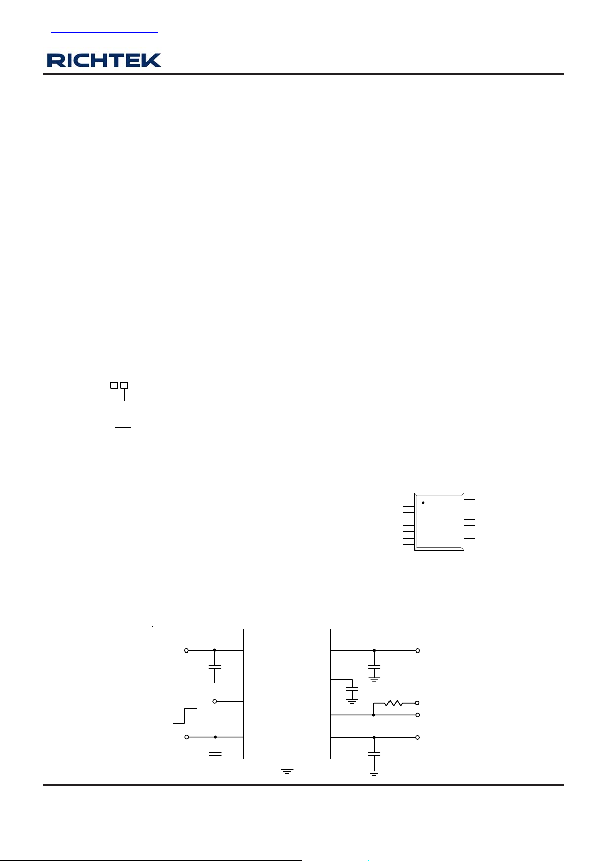
Pin Configurations
(TOP VIEW)
SOP-8
8
EN1
7
GND
6
VDOUT
5
VOUT2
VIN1
VOUT1
Cd
VIN2
2
3
4
Typical Application Circuit
Cd
2
3
6
Cd
C
1uF1uF
100k
C
1uF
OUT1
R1
OUT2
V
V
V
V
OUT1
IN2
DOUT
OUT2
V
IN1
C
IN1
Chip Enable
V
IN2
C
IN2
1uF
1
VIN1
RT9002A/B/C
8
EN1
45
VIN2 VOUT2
VOUT1
VDOUT
GND
7
DS9002ABC-03 March 2007 www.richtek.com
1
Page 2
RT9002A/B/C
Functional Pin Description
Pin No. Pin Name Pin Function
1 VIN1 Channel 1 Supply Input.
2 VOUT1 Channel 1 Output Voltage.
3 Cd Delay Capacitor.
4 VIN2 Channel 2 Supply Voltage.
5 VOUT2 Channel 2 Output Input.
6 VDOUT Detector Output Voltage. (RT9002A = Active High, RT9002B and RT9002C = Active Low)
7 GND Common Ground.
8 EN1 Chip Enable (Active High) for Channel 1.
Function Block Diagram
EN1
Cd
VDOUT
Shutdown
and
Logic Control
V
REF
+
-
Error
Amplifier
+
-
Amplifier
-
+
Comparator
Error
V
REF
VD
MOS Driver
Current-Limit
and
Thermal
Protection
MOS Driver
Current-Limit
and
Thermal
Protection
VIN1
VOUT1
VIN2
VOUT2
GND
DS9002ABC-03 March 2007www.richtek.com
2
Page 3
RT9002A/B/C
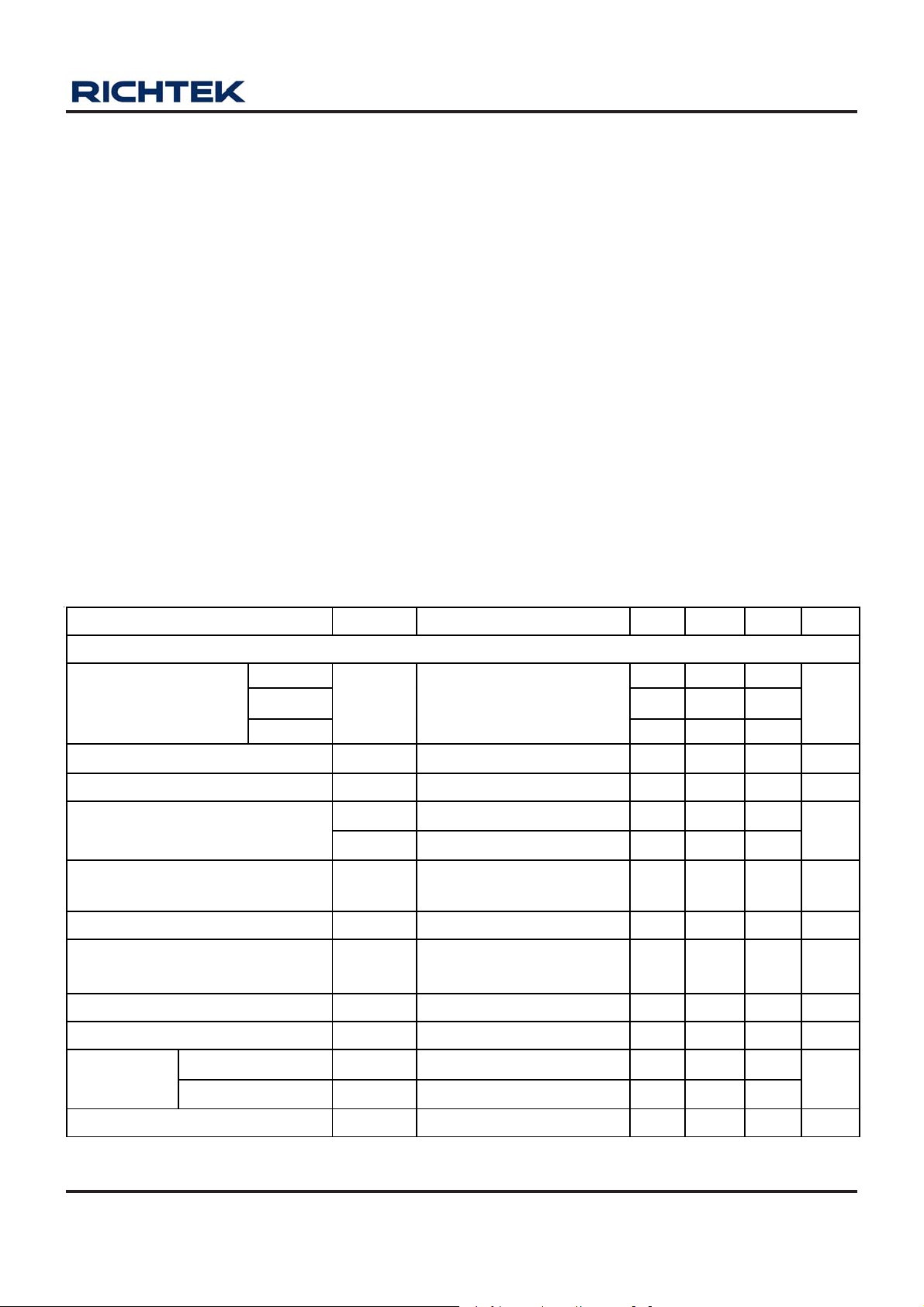
Absolute Maximum Ratings (Note 1)
z Supply Input Voltage-------------------------------------------------------------------------------------------------- 6V
z Package Thermal Resistance (Note 4)
SOP-8, θJA-------------------------------------------------------------------------------------------------------------- 110°C/W
z Power Dissipation, P
SOP-8 -------------------------------------------------------------------------------------------------------------------- 0.909W
z Lead Temperature (Soldering, 10 sec.) --------------------------------------------------------------------------- 260°C
z Junction Temperature ------------------------------------------------------------------------------------------------- 150°C
z Storage Temperature Range ---------------------------------------------------------------------------------------- −65°C to 150°C
z ESD Susceptibility (Note 2)
HBM (Human Body Mode) ------------------------------------------------------------------------------------------ 2kV
MM (Machine Mode) -------------------------------------------------------------------------------------------------- 200V
Recommended Operating Conditions (Note 3)
z Supply Input Voltage -------------------------------------------------------------------------------------------------- 2.5V to 5.5V
z Chip Enable Input Voltage ------------------------------------------------------------------------------------------- 0V to 5.5V
z Junction Temperature Range ---------------------------------------------------------------------------------------- −40°C to 125°C
z Ambient Temperature Range ---------------------------------------------------------------------------------------- −40°C to 125°C
@ T
D
= 25°C
A
Electrical Characteristics
(V
= V
IN
+ 1V, whichever is greater, CIN = 1μF, C
OUT
Parameter Symbol Test Conditions Min Typ Max Units
Regulator 1
RT9002A 2.45 2.50 2.55
Output Voltage Accuracy
RT9002B 1.47 1.50 1.53
ΔV
OUT1
RT9002C
Maximum Output Current I
Load Regulation (Note 5) ΔV
Dropout Voltage (Note 6)
OUT1_MAX
LOAD1
V
DROP1_1
V
DROP1_2
Quiescent Current (Note 7) IQ1
Standby Current I
Line Regulation ΔV
STB1
LINE1
Power Supply Rejection Rate PSRR1 f = 100Hz, I
Current Limit I
LIM1
Logic-Low Voltage VIL -- -- 0.6
EN Threshold
Logic-High Voltage V
Thermal Shutdown Protection T
IH
SD1
= 1μF, TA = 25°C, unless otherwise specified)
OUT
I
OUT1
= 30mA
240 -- -- mA
1mA < I
I
OUT1
I
OUT1
V
I
OUT1
V
V
V
V
OUT1
= 30mA -- 50 --
= 100mA -- 150 --
= V
IN1
= 0mA
= 3.5V, V
IN1
= 3.5V to 5.5V,
IN1
= V
IN1
= V
IN1
1.8 -- --
-- 170 -- °C
2.45 2.50 2.55
< 100mA -- 1 -- mV
= 3.5V,
EN1
= 0V -- 0.1 1 μA
EN1
, I
EN1
OUT1
EN1
= 30mA
OUT1
= 100mA -- −60 -- dB
= 5V -- 450 -- mA
-- 30 -- μA
-- 0.01 0.2 %/V
To be continued
V
mV
V
DS9002ABC-03 March 2007 www.richtek.com
3
Page 4
RT9002A/B/C
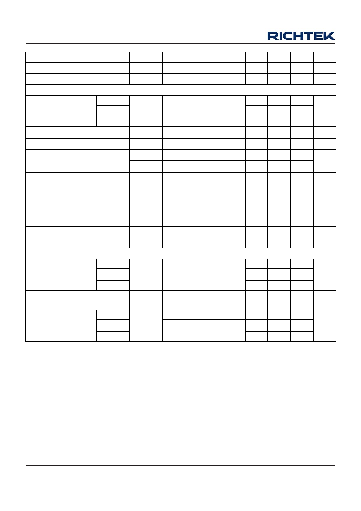
Parameter Symbol Test Conditions Min Typ Max Units
Thermal Shutdown Hysteresis
ΔT
SD1
Enable Pin Current IEN V
-- 40 --
= 3.5V, Enable -- 0.1 1 μA
IN
Regulator 2
RT9002A 3.234 3.30 3.366
Output Voltage Accuracy
RT9002B 2.744 2.80 2.856
ΔV
OUT2
I
OUT2
= 30mA
RT9002C
Maximum Output Current I
Load Regulation (Note 5) ΔV
Dropout Voltage (Note 6)
OUT2_MAX
LOAD2
V
DROP2_1
V
DROP2_2
Quiescent Current (Note 7) IQ2 V
Line Regulation ΔV
LINE2
500 -- -- mA
1mA < I
I
OUT2
I
OUT2
V
I
OUT2
OUT2
= 30mA -- 50 90
= 100mA -- 150 200
= 4.3V, I
IN2
= 4.3V to 5.5V,
IN2
= 30mA
Power Supply Rejection Rate PSRR2 f = 100Hz, I
Current Limit I
Thermal Shutdown Protection T
Thermal Shutdown Hysteresis
V
LIM2
-- 170 -- °C
SD2
ΔT
SD2
= 5V -- 800 -- mA
IN2
-- 40 --
Detector
°C
3.234 3.30 3.366
< 100mA -- 15 50 mV
mV
= 0mA -- 40 -- μA
OUT2
-- 0.01 0.2 %/V
= 100mA -- −60 -- dB
OUT2
V
°C
RT9002A 3.528 3.60 3.672
Detect Fall Voltage
RT9002B 3.822 3.9 3.978
VDF
RT9002C
Hysteresis ΔV
RT9002A V
Sink Current
RT9002B 4.0 8.0 --
I
DOUT
RT9002C
HYS
DOUT
V
DOUT
= 0.5V, V
= 0.5V, V
3.528 3.60 3.672
V
DF
x0.02
= 5.0V 7.0 12.0 --
IN2
= 2.0V
IN2
V
DF
x0.05
4.0 8.0 --
V
DF
x0.08
V
V
mA
DS9002ABC-03 March 2007www.richtek.com
4
Page 5

RT9002A/B/C
Note 1. Stresses listed as the above “Absolute Maximum Ratings” may cause permanent damage to the device. These are for
stress ratings. Functional operation of the device at these or any other conditions beyond those indicated in the
operational sections of the specifications is not implied. Exposure to absolute maximum rating conditions for extended
periods may remain possibility to affect device reliability.
Note 2. Devices are ESD sensitive. Handling precaution recommended.
Note 3. The device is not guaranteed to function outside its operating conditions.
Note 4. θ
Note 5. Regulation is measured at constant junction temperature by using a 20ms current pulse. Devices are tested for load
Note 6. The dropout voltage is defined as V
Note 7. Quiescent, or ground current, is the difference between input and output currents. It is defined by I
is measured in the natural convection at TA = 25°C on a high effective thermal conductivity test board of JEDEC
JA
51-7 2S2P 4-layer thermal measurement standard.
regulation in the load range from 1mA to 100mA.
-V
load condition (I
IN
= 0mA). The total current drawn from the supply is the sum of the load current plus the ground pin
OUT
, which is measured when V
OUT
OUT
is V
OUT(NORMAL)
− 100mV.
= IIN - I
Q
OUT
current.
under no
DS9002ABC-03 March 2007 www.richtek.com
5
Page 6

RT9002A/B/C
Typical Operating Characteristics
Input Voltage vs. Detector Voltage
7
RT9002A
6
5
4
3
2
Reset Voltage (V)
1
0
0123456
Input Voltage (V)
Output Voltage vs. Temperature
3.6
RT9002A
3.4
3.2
3.0
2.8
2.6
Output Voltage (V)
2.4
2.2
-50 -25 0 25 50 75 100 125
Temperature
(°C)
V
V
OUT2
OUT1
125
Input Voltage vs. Detector Voltage
7
RT9002B
6
5
4
3
2
Reset Voltage (V)
1
0
0123456
Input Voltage (V)
Output Voltage v s . Te m perature
3.0
RT9002B
2.8
2.6
2.4
2.2
2.0
1.8
Output Voltage (V)
1.6
1.4
-50 -25 0 25 50 75 100 125
Temperature
(°C)
V
V
OUT2
OUT1
Qu iesc ent Current vs. Inp ut Voltage
45
RT9002A
42.5
40
V
V
OUT2
OUT1
37.5
35
32.5
30
Quiescent Current (uA)
27.5
25
2.5 3 3.5 4 4.5 5 5.5
Input Voltage (V)
42.5
37.5
32.5
Quiescent Current (uA)
27.5
Qu iesc ent Current vs. Input Voltage
45
RT9002B
V
V
OUT2
OUT1
40
35
30
25
2.533.544.555.5
Input Voltage (V)
DS9002ABC-03 March 2007www.richtek.com
6
Page 7

RT9002A/B/C
Nch Driver Sink Current vs. Input Voltage
60
RT9002A
50
40
30
20
10
-40°C
25°C
125°C
Nch Driver Output Current (mA)
0
0123456
Input Voltage (V)
Nch Driver Sink Current vs. V
200
RT9002A
175
150
125
100
75
50
25
Nch Driver Output Current (mA)
0
0123456
VDD = 5V
VDS (V)
VDD = 5.5V
VDD = 4.5V
DS
Nch Dr iver Sink Current vs. Input Voltage
60
RT9002B
50
40
30
20
10
Nch Driver Output Current (mA)
0
0123456
Input Voltage (V)
Nch Driver Sink Current vs. V
110
RT9002B
100
90
80
70
60
50
40
30
20
10
Nch Driver Output Current (mA)
0
01234 56
-40°C
25°C
125°C
VDD = 0.5V
VDS (V)
DS
VDD = 3.5V
VDD = 3V
VDD = 2.5V
VDD = 2V
VDD = 1.5V
VDD = 1V
Output Delay Time v s . Load Capac itance
1000
RT9002A
100
10
1
0.1
Output Delay Time (ms)
0.01
0.0000 0.0001 0.0010 0.0100 0.1000
Load Capacitance (uF)
Output Delay Time vs. Load Capacitance
1000
RT9002B
100
10
1
0.1
Output Delay Time (us)
0.01
0.0000 0.0001 0.0010 0.0100 0.1000
Load Capacitance (uF)
DS9002ABC-03 March 2007 www.richtek.com
7
Page 8

RT9002A/B/C
Dropout Voltage vs. Load Current
400
RT9002A, V
350
300
250
200
150
100
Dropout Voltage (mV)
50
0
0 50 100 150 200 250 300
OUT1
= 2.5V
Load Current (mA)
EN Pin Shutdown Response
RT9002A, V
I
LOAD
(5V/Div)
= 75mA
OUT1
125°C
25°C
-40°C
600
500
400
300
200
Dropout Voltage (mV)
100
V
OUT
(1V/Div)
Dropout Voltage vs. Load Current
RT9002C, V
0
0 0.1 0.2 0.3 0.4 0.5
= 3.3V
OUT2
Load Current (A)
125°C
25°C
-40°C
Line Transient Response
RT9002A
Boost I
5
4
LOAD
= 50mA
Shutdown Voltage
OUT
V
I
OUT1
(100mA/Div)
V
OUT1
(5mV/Div)
V
OUT2
(50mV/Div)
(1V/Div)
RT9002A
I
LOAD
Time (100μs/Div)
Load Transient Response
= 10mA to 100mA
V
OUT1
(20mV/Div)
V
OUT2
(20mV/Div)
Shutdown Voltage
OUT
V
RT9002A, V
I
LOAD
(5V/Div)
(1V/Div)
= 75mA
Time (250μs/Div)
Start Up
OUT1
Time (500μs/Div)
Time (10μs/Div)
DS9002ABC-03 March 2007www.richtek.com
8
Page 9

RT9002A/B/C
600
40 0
200
-200
Noise (μV/Div)
-400
-600
RT9002B, V
I
OUT1
0
= 100mA
Noise
OUT1
Time (10ms/Div)
600
40 0
200
-200
Noise (μV/Div)
-400
-600
RT9002B, V
No Load
0
Noise
OUT1
Time (10ms/Div)
DS9002ABC-03 March 2007 www.richtek.com
9
Page 10

RT9002A/B/C
Applications Information
Like any low-dropout regulator, the external capacitors used
with the RT9002A/B/C must be carefully selected for
regulator stability and performance. Using a capacitor
whose value is > 1μF on the RT9002A/B/C input and the
amount of capacitance can be increased without limit. The
input capacitor must be located a distance of not more
than 0.5 inch from the input pin of the IC and returned to a
clean analog ground. Any good quality ceramic can be
used for this capacitor. The capacitor with larger value and
lower ESR (equivalent series resistance) provides better
PSRR and line-transient response.
The output capacitor must meet both requirements for
minimum amount of capacitance and ESR in all LDOs
application. The RT9002A/B/C is designed specifically to
work with low ESR ceramic output capacitor in space-
saving and performance consideration. Using a ceramic
capacitor whose value is at least 1μF with ESR is > 20mΩ
on the RT9002A/B/C output ensures stability. The
RT9002A/B/C still works well with output capacitor of other
types due to the wide stable ESR range. Figure 1. shows
the curves of allowable ESR range as a function of load
current for various output capacitor values. Output capacitor
of larger capacitance can reduce noise and improve load
transient response, stability, and PSRR. The output
capacitor should be located not more than 0.5 inch from
the VOUT pin of the RT9002A/B/C and returned to a clean
analog ground.
Enable
The RT9002A/B/C goes into sleep mode when the Enable
pin is in a logic low condition. During this condition, the
pass transistor, error amplifier, and bandgap are turned off,
reducing the supply current to 0.1μA typical. The Enable
pin may be directly tied to VIN to keep the part on. The
Enable input is CMOS logic and cannot be left floating.
PSRR
The power supply rejection ratio (PSRR) is defined as the
gain from the input to output divided by the gain from the
supply to the output. The PSRR is found to be
⎛
Δ
×=
log20PSRR
⎜
Δ
Supply
⎝
⎞
Error Gain
⎟
⎠
Note that when heavy load measuring, Δsupply will cause
Δtemperature. And Δtemperature will cause Δoutput
voltage. So the heavy load PSRR measuring is include
temperature effect.
Current Limit
The RT9002A/B/C contains an independent current limiter,
which monitors and controls the pass transistor's gate
voltage, limiting the output1/2 current to 0.45/0.8A (typ.).
The output can be shorted to ground indefinitely without
damaging the part.
Thermal-Shutdown Protection
Region of Stable C
100
10
ESR (Ω)
ESR (Ω)
OUT
1
OUT
0.1
0.01
Region of Stable C
Region of Stable C
0.001
0 50 100 150 200 250 300
10
ESR vs. Load Current
OUT
RT9002APS
V
= 4.0V, V
IN
C
= C
IN
OUT
Unstable Region
Stable Region
Unstable Region (Simulation Verify)
Load Current (mA)
= 3.3V
OUT2
= 1uF/X7R
Figure 1
Thermal-shutdown protection limits total power dissipation
in the RT9002A/B/C. When the junction temperature
exceeds TJ = +170°C, the thermal sensor signals the
shutdown logic, turning off the pass transistor and allowing
the IC to cool. The thermal sensor turns the pass transistor
on again after the IC's junction temperature cools by 40°C,
resulting in a pulsed output during continuous thermal
overload conditions. Thermal-shutdown protection is
designed to protect the RT9002A/B/C in the event of fault
conditions. For continual operation, do not exceed the
absolute maximum junction temperature rating of TJ =
+125°C.
DS9002ABC-03 March 2007www.richtek.com
Page 11

Outline Dimension
RT9002A/B/C
A
J
I
Dimensions In M illimeters Dimensions In Inches
Symbol
Min Max Min Max
A 4.801 5.004 0.189 0.197
B
F
C
D
H
M
B 3.810 3.988 0.150 0.157
C 1.346 1.753 0.053 0.069
D 0.330 0.508 0.013 0.020
F 1.194 1.346 0.047 0.053
H 0.170 0.254 0.007 0.010
I 0.050 0.254 0.002 0.010
J 5.791 6.200 0.228 0.244
M 0.400 1.270 0.016 0.050
Richtek Technology Corporation
Headquarter
5F, No. 20, Taiyuen Street, Chupei City
Hsinchu, Taiwan, R.O.C.
Tel: (8863)5526789 Fax: (8863)5526611
8-Lead SOP Plastic Package
Richtek Technology Corporation
Taipei Office (Marketing)
8F, No. 137, Lane 235, Paochiao Road, Hsintien City
Taipei County, Taiwan, R.O.C.
Tel: (8862)89191466 Fax: (8862)89191465
Email: marketing@richtek.com
DS9002ABC-03 March 2007 www.richtek.com
11
 Loading...