

Page 1
®
RT8885A
Dual Output 3-Phase + 2-Phase PWM Controller
and GPU Core Power Supply
General Description
The RT8885A is a dual output 3-phase + 2-phase PWM
controller with 3 integrated MOSFET gate drivers and a
single SVID interface for CPU and GPU core power supply.
This part complies with Intel VR12/IMVP7 Pulse Width
Modulation Specification. The RT8885A adopts G-NAVP
(Green-Native AVP), which is a Richtek proprietary topology
derived from finite DC gain compensator in constant on-
time control mode. G-NAVPTM makes this part an easy-
setting PWM controller to meet all Intel mobile CPU/GPU
AVP (Active Voltage Positioning) requirements. The
RT8885A uses SVID interface to control an internal 8-bit
DAC for output voltage programming. The built-in high
accuracy DAC converts the VID code to a reference voltage
ranging from 0V to 1.52V with 5mV step voltage. The
system accuracy of the controller reaches 0.8%. Each
output channel of the RT8885A can operate in multi-phase
continuous conduction mode or in single-phase diode
emulation mode to reach a maximum of 90% efficiency in
different load conditions. The droop function (load line) is
selectable and the load line is easily programmed by setting
the DC gain of the error amplifier. With proper
compensation, the load transient response can achieve
optimized AVP performance. The output voltage transition
slew rate is programmed via the SVID interface. The
RT8885A supports inductor DCR and sense-resistor
current sensing. This device provides power good
indication, current monitor, thermal monitor and thermal
throttling output signals for IMVP7 CPU and GPU core.
This part also provides complete fault protection functions
including over voltage, under voltage, negative voltage, over
current, thermal shutdown and under voltage lockout.
TM
Features
Dual Output : 3-Phase (CORE) + 2-Pha se (GFX)
Integrated MOSFET Drivers : 2 (CORE) + 1 (GFX)
VR12/IMVP7 PWM Specification Compliant
Serial VID Interface
G-NAV P
Fast Line/Load Transient Response
Quick Response for Load Transient
0.5% DAC Accuracy
0.8% System Accuracy
Accurate Current Balance
Selectable Droop Function
Selectable Forced DEM Operation
Built-in ADC for Platform Programming
Power Good Indicator
Current Monitor Output
Thermal Monitor
Thermal Throttling Indicator VRHOT
Phase Shedding in PS1
Phase Shedding and Diode Emulation in PS2
Differential Remote Output Voltage Sense
Lossless Inductor DCR Current Sense
Switching Frequency up to 1MHz per Phase
OVP, UVP, NVP, OCP, OTP, UVLO
56-Lead WQFN Package
RoHS Compliant and Halogen Free
TM
T opology
Applications
IMVP7 Intel CPU/CPU Core Power Supply
Laptop Computer
AVP Step-Down Converter
For CPU
Simplified Application Circuit
V
GFX
Copyright 2014 Richtek Technology Corporation. All rights reserved. is a registered trademark of Richtek Technology Corporation.
©
Buck A1
Buck A2
RT8885A
PWMA2 Driver Bus #2
SVID BusFrom CPU
DS8885A-01 January 2014 www.richtek.com
Driver Bus #1Driver Bus #A1
PWM3
Buck 1
Buck 2
Buck 3
V
CORE
1
Page 2
RT8885A
Ordering Information
RT8885A
Package Type
QW : WQFN-56L 7x7 (W-Type)
Lead Plating System
Z : ECO (Ecological Element with
Halogen Free and Pb free)
Note :
Richtek products are :
RoHS compliant and compatible with the current require-
ments of IPC/JEDEC J-STD-020.
Suitable for use in SnPb or Pb-free soldering processes.
Pin Configurations
UGATEA
PHASEA
LGATEA
PWMA2
TONSETA
ISENA2P
ISENA2N
ISENA1P
ISENA1N
COMPA
FBA
RGNDA
IMONA
VSENA
VDIO
ALERT
VCLK
BOOTA
1
2
3
4
5
6
7
8
9
10
11
12
13
14
Marking Information
(TOP VIEW)
PVCC2
BOOT2
UGATE2
PHASE2
LGATE2
PGND
RT8885A
ZQW
YMDNN
PHASE1
PVCC1
LGATE1
454647484950515253545556
44 43
57
262524232221201918171615
27 28
BOOT1
UGATE1
42
41
40
39
38
37
36
35
34
33
32
31
30
29
RT8885AZQW : Product Number
YMDNN : Date Code
PWM3
TONSET
ISEN2P
ISEN2N
ISEN1N
ISEN1P
ISEN3P
ISEN3N
VSEN
COMP
FB
RGND
IMON
VREF/QRTH
EN
VCC
SET1
TSEN/ZLL
SET2
RSET/OFS
RSETA/OFSA
IBIAS
AGND
OCSET
VRHOT
VR_READY
VRA_READY
TSENA/ZLLA
WQFN-56L 7x7
Copyright 2014 Richtek Technology Corporation. All rights reserved. is a registered trademark of Richtek Technology Corporation.
©
DS8885A-01 January 2014www.richtek.com
2
Page 3

RT8885A
Functional Pin Description
Pin No. Pin Name Pin Function
1 PWMA2
2 TON SETA
3, 5 ISENA[2:1]P Positive Current Sense Input for Channel 2 and Channel 1 of GFX VR.
4, 6 ISENA[2:1]N
7 COMPA GFX VR Compensation Pin. This pin is the output of the error amplifier.
8 FBA
9 RGN DA
10 IMONA
11 VSENA
12 VDIO
13
14 VCLK
15 VRA_READ Y
16 VR_READY
17
18 IBIAS
19 TSENA/ZLLA
20 OCSET
21 AGND Analog Ground Pin.
22 TSEN/ZLL
Copyright 2014 Richtek Technology Corporation. All rights reserved. is a registered trademark of Richtek Technology Corporation.
DS8885A-01 January 2014 www.richtek.com
©
ALER T
VRHOT
GFX VR Channel 2 PWM Signal Output. Connect this pin to the PWM input
of external MOSFET driver for channel 2 of GFX VR.
GFX VR PWM On-Time Setting Pin. Connect this pin to input voltage VIN via
a resistor to set the ripple size of GFX VR output in CCM.
Negative Current Sense Input Pin for Channel 2 and Channel 1 of GFX VR.
ISENA2N can be pulled high to VCC to disable GFX VR channel 2. Connect
to this pin with a sense resistor of 680.
GFX VR Output Voltage Feedback Pin. Connect this pin to the CPU voltage
remote sense pin with a resistor. This pin is the inverting input node of the
error amplifier.
Return Ground for GFX VR. This pin is the inverting input node for differential
remote voltage sensing.
GFX VR Current Monitor Output. Connect a thermally compensated resistor
network from this pin to VREF/QRTH pin. IMONA pin output voltage V
is proportional to the total output current of GFX VR.
GFX VR Output Voltage Sensing Pin. Voltage on this pin is monitored for
voltage-related protections.
Data Transmission Line of SVID Interface. This pin has an open drain
structure. Pull high this pin to platform VCCIO rail with a resistor placed close
to controller.
Alert Line of the SVID Interface (Active Low). This pin has an open drain
structure. Pull high this pin to platform VCCIO rail with a resistor placed close
to controller.
Clock Signal Line of SVID Interface. This pin has an open drain structure. Pull
high VCLK to platform VCCIO rail with a resistor placed close to controller.
GFX VR Power Good Indicator Output. This pin has an open drain structure.
Pull high this pin to platform VCCIO rail with a resistor.
CORE VR Power Good Indicator Output. This pin has an open drain
structure. Pull high this pin to platform VCCIO rail with a resistor.
Thermal Throttling Output (Active Low). This pin has an open drain structure.
Pull high this pin to platform VCCIO rail with a resistor.
Internal Bias Current Setting Pin. Connect this pin to GND only with a 53.6k
resistor placed close to the controller.
This Pin Provides Two Functions for GFX VR : Thermal Monitor Input, and
Droop Enable/Disable Setting. Connect a thermally compensated resistive
voltage divider from VCC to GND and connect the joint of the voltage divider
to this pin.
CORE VR and GFX VR Over Current Protection Threshold Setting Pin.
Connect a resistive voltage divider from VCC to GND and connect the joint of
the voltage divider to this pin to set summed total over current protection
threshold and per phase over current protection threshold for CORE VR and
GFX VR individually.
This Pin Provides Two Functions for CORE VR : Thermal Monitor Input, and
Droop Enable/Disable Setting. Connect a thermally compensated resistive
voltage divider from VCC to GND and connect the joint of the voltage divider
to this pin.
IMONA
3
Page 4

RT8885A
Pin No. Pin Name Pin Func ti on
This pin provides three settings for GFX VR : internal compensation ramp
23 RSETA/OFSA
24 RSET/OFS
25 SET2
26 SET1
27 VCC
28 EN Voltage Regulator Enable Signal Input.
29 VREF/QRTH
30 IMON
31 RGND
32 FB
33 COMP CORE VR Compensation Pin. This pin is the output of the error amplifier.
34 VSEN
35, 39, 38 ISEN[3:1]N
36, 40, 37 ISEN[3:1]P Positive current sense input for channel 3, 2 and 1 of CORE VR.
41 TONSET
42 PWM3
43 BOOT1
44 UGATE1
factor for control loop, output voltage offset and forced-DEM operation.
Connect a resistive voltage divider from VCC to GND and connect the joint
of the voltage divider to this pin.
This pin provides three settings for CORE VR : internal compensation
ramp factor for control loop, output voltage offset and forced-DEM
operation. Connect a resistive voltage divider from VCC to GND and
connect the joint of the voltage divider to this pin.
This pin provides three settings for GFX VR : initial startup voltage
V
INI_GFX
, maximum output current ICCMAXA and PWM on-time of quick
response for load transient response boost. Connect a resistive voltage
divider from VCC to GND, and connect the joint of the voltage divider to
this pin.
This pin provides three settings for CORE VR : Initial startup voltage
V
INI_CORE
, maximum output current ICCMAX and PWM on-time of quick
response for load transient response boost. Connect a resistive voltage
divider from VCC to GND and connect the joint of the voltage divider to
this pin.
Controller Power Supply Pin. Connect this pin to GND with a ceramic
capacitor larger than 1F.
This Pin Provides Two Functions : Fixed 0.6V Reference Voltage Output,
and Quick Response Trigger Threshold Setting. Connect a resistive
voltage divider from VCC to GND and connect the joint of the voltage
divider to this pin. Bypass this pin to GND with ceramic capacitor for noise
decoupling.
CORE VR Current Monitor Output. Connect a thermally compensated
resistor network from this pin to VREF/QRTH pin. IMON pin output voltage
V
is proportional to the total output current of CORE VR.
IMON
Return Ground for CORE VR. This pin is the inverting input node for
differential remote voltage sensing.
CORE VR Feedback Pin. This pin is the inverting input node of the error
amplifier.
CORE VR output voltage sensing pin. Voltage on this pin is monitored for
voltage related protections.
Negative Current Sense Input Pin for Channel 3, 2 and 1 of CORE VR.
ISENA2N and ISENA3N can be pulled high to VCC to disable CORE VR
channel 2 and channel 3, respectively. Connect to this pin with a sense
resistor of 680.
CORE VR PWM On-Time Setting Pin. Connect this pin to input voltage
VIN via a resistor to set the ripple size of CORE VR output in CCM.
CORE VR Channel 3 PWM Signal Output. Connect this pin to the PWM
input of external MOSFET driver for channel 3 of CORE VR.
CORE VR Channel 1 Bootstrap Flying Capacitor Connection Pin. This pin
powers channel 1 high side MOSFET drivers. Connect this pin to PHASE1
pin wi th a cer amic capacitor.
CORE VR Channel 1 High Side MOSFET Floating Gate Driver Output.
Connect this pin to the gate of high side MOSFET of channel 1.
Copyright 2014 Richtek Technology Corporation. All rights reserved. is a registered trademark of Richtek Technology Corporation.
4
©
DS8885A-01 January 2014www.richtek.com
Page 5

Pin No. Pin Name Pin Function
CORE VR Channel 1 Switching Node Connection Pin. Connect this pin to
45 PHASE1
46 LGATE1
47 PVCC1
48 LGATE2
49 PHASE2
50 UGATE2
51 BOOT2
52 PVCC2
53 LGATEA
54 PHASEA
55 UGATEA
56 BOOTA
57
(Exposed Pad)
PGND
the joint of high side MOSFET sources, the low side MOSFET drains and
the inductor of channel 1.
CORE VR Channel 1 Low Side MOSFET Gate Driver Output. Connect
this pin to the gate of low side MOSFET of channel 1.
CORE VR Embedded MOSFET Driver Power Supply Pin. This pin
powers channel 1 and channel 2 MOSFET gate drivers. Connect this pin
to GND with a ceramic capacitor larger than 1μF.
CORE VR Channel 2 Low Side MOSFET Gate Driver Output. Connect
this pin to the gate of low side MOSFET of channel 2.
CORE VR Channel 2 Switching Node Connection Pin. Connect this pin to
the joint of high side MOSFET sources, the low side MOSFET drains and
the inductor of channel 2.
CORE VR Channel 2 High Side MOSFET Floating Gate Driver Output.
Connect this pin to the gate of high side MOSFET of channel 2.
CORE VR Channel 2 Bootstrap Flying Capacitor Connection Pin. This pin
powers channel 2 high side MOSFET drivers. Connect this pin to
PHASE2 pin with a ceramic capacitor.
GFX VR Embedded MOSFET Driver Power Supply Pin. Connect this pin
to GND with a ceramic capacitor larger than 1F.
GFX VR Channel 1 Low Side MOSFET Gate Driver Output. Connect this
pin to the gate of low side MOSFET of channel 1.
GFX VR Channel 1 Switching Node Connection Pin. Connect this pin to
the joint of high side MOSFET sources, the low side MOSFET drains and
the inductor of channel 1.
GFX VR Channel 1 High Side MOSFET Floating Gate Driver Output.
Connect this pin to the gate of high side MOSFET of channel 1.
GFX VR Channel 1 Bootstrap Flying Capacitor Connection Pin. This pin
powers channel 1 high side MOSFET drivers. Connect this pin to
PHASEA pin with a ceramic capacitor.
Power Ground. The exposed pad is the return ground of all low side
MOSFET gate drivers. This exposed pad must be soldered to a large
PCB and connected to GND for maximum power dissipation.
RT8885A
Copyright 2014 Richtek Technology Corporation. All rights reserved. is a registered trademark of Richtek Technology Corporation.
DS8885A-01 January 2014 www.richtek.com
©
5
Page 6
RT8885A
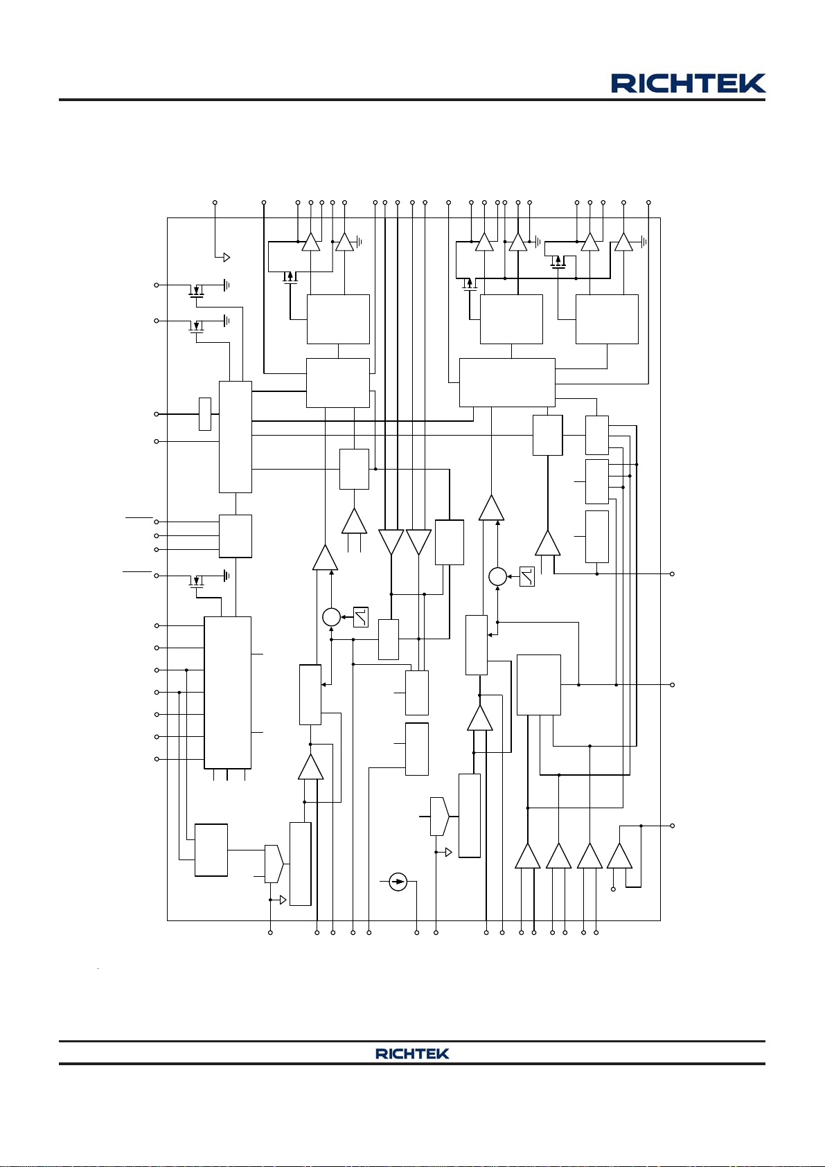
Function Block Diagram
AGND
VR_READY
PWMA2
BOOTA
UGATEA
PHASEA
PVCC2
LGATEA
TONSETA
ISENA1P
ISENA1N
ISENA2P
ISENA2N
TONSET
BOOT1
UGATE1
PHASE1
PVCC1
LGATE1
PGND
BOOT2
UGATE2
PHASE2
LGATE2
PWM3
VRA_READY
VCC
EN
ALERT
VDIO
VCLK
VRHOT
TSEN/ZLL
TSENA/ZLLA
RSETA/OFSA
RSET/OFS
OCSET
SET1
SET2
UVLO
Control & Protection Logic
SVID
ADC
XCVR
VQRTH VQRTHA
PWM
Offset
AMP
ERROR
+
CMP
+
Cancellation
-
Driver
TON
QR
-
+
Logic
Generator
Phase
Selector
CMP
+
-
VSENA
VQRTHA
+-+
SUM
To Protection Logic
Current
OCPOV/UV/NV
Logic
Driver
Balance
VSEN
IMON
Logic
Driver
TON
Generator
Phase
Selector
CMP
PWM
+
-
-
Current
Balance
QR
CMP
+
-
To Protection Logic
+
VQRTH
Offset
Cancellation
OCPOV/UV/NVIBIAS
AMP
ERROR
+
-
VSET
SUM
IMON
QRTH
VREF/
IMONA
Offset
Generator
Logic
From Control
Copyright 2014 Richtek Technology Corporation. All rights reserved. is a registered trademark of Richtek Technology Corporation.
©
DAC
RGNDA
VSETA
Rate Control
Soft-Start & Slew
FBA
COMPA
IMONA
VSENA
DAC
Rate Control
RGND
Soft-Start & Slew
+
-
+-+-+
FB
COMP
ISEN3P
ISEN2P
ISEN3N
ISEN1P
ISEN2N
-
0.6V
ISEN1N
From Control Logic
VREF/QRTH
DS8885A-01 January 2014www.richtek.com
6
Page 7

Operation
RT8885A
The RT8885A adopts G-NAVPTM (Green-Native AVP),
which is a Richtek proprietary topology derived from finite
DC gain compensator in constant on-time control mode.
G-NAVPTM is based on the finite gain peak current mode
with CCRCOT (Constant Current Ripple Constant On-Time)
topology. The control loop consists of PWM modulators
with power stages, current sense amplifiers and an error
amplifier as shown in functional block diagram. The
HS_FET on-time is determined by CCRCOT on-time
generator. Low offset current sense amplifiers are used
for current balance, loop control and over current detection.
By increasing the loading current, the current signal is
rose to increase the steady state COMP voltage, and then
the output voltage is decreased to achieving AVP.
A near-DC offset canceling is added to the output of EA to
eliminate the inherent output offset of finite gain peak
current mode controller. After EN go high, the internal ADC
sense pin setting for VINITAL, ICCMAX, over current
protection and internal compensation ramp setting. The
internal ADC also sense IMON and TSEN pin voltage for
INTEL reporting.
Copyright 2014 Richtek Technology Corporation. All rights reserved. is a registered trademark of Richtek Technology Corporation.
DS8885A-01 January 2014 www.richtek.com
©
7
Page 8

RT8885A
Table 1. VR12/IMVP7 Compliant VID Table
VID7 VID6 VID5 VID4 VID3 VID2 VID1 VID0 H 1 H0 DAC Voltage (V)
0
0
0
0
0
0
0
0
0
0
0
0
0
0
0
0
0
0
0
0
0
0
0
0
0
0
0
0
0
0
0
0
0
0
0
0
0
0
0
0
0
0
0
0
0
0
0
0
0
0
0
0
0
0
0
0
0
0
0
0
0
0
0
0
0
0
0
0
0
0
0
0
0
0
0
0
0
0
0
0
0
0
0
0
0
0
0
0
0
0
0
0
0
0
0
0
0
0
0
0
0
0
0
0
0
0
0
0
0
0
0
0
0
0
0
0
0
0
0
0
0
0
1
1
1
1
1
1
1
1
1
1
1
1
1
0
0
0
0
0
0
0
0
0
0
0
0
0
0
0
0
1
1
1
1
1
1
1
1
1
1
1
1
1
1
1
1
0
0
0
0
0
0
0
0
0
0
0
0
0
0
0
0
0
0
0
0
0
1
1
1
1
1
1
1
1
0
0
0
0
0
0
0
0
1
1
1
1
1
1
1
1
0
0
0
0
0
0
0
0
1
1
1
1
1
0
0
0
0
1
1
1
1
0
0
0
0
1
1
1
1
0
0
0
0
1
1
1
1
0
0
0
0
1
1
1
1
0
0
0
0
1
1
1
1
0
0
0
0
1
0
0
1
1
0
0
1
1
0
0
1
1
0
0
1
1
0
0
1
1
0
0
1
1
0
0
1
1
0
0
1
1
0
0
1
1
0
0
1
1
0
0
1
1
0
0
0 0 0.000
1
0 1 0.250
0
0 2 0.255
1
0 3 0.260
0
0 4 0.265
1
0 5 0.270
0
0 6 0.275
1
0 7 0.280
0
0 8 0.285
1
0 9 0.290
0
0 A 0.295
1
0 B 0.300
0
0 C 0.305
1
0 D 0.310
0
0 E 0.315
1
0 F 0.320
0
1 0 0.325
1
1 1 0.330
0
1 2 0.335
1
1 3 0.340
0
1 4 0.345
1
1 5 0.350
0
1 6 0.355
1
1 7 0.360
0
1 8 0.365
1
1 9 0.370
0
1 A 0.375
1
1 B 0.380
0
1 C 0.385
1
1 D 0.390
0
1 E 0.395
1
1 F 0.400
0
2 0 0.405
1
2 1 0.410
0
2 2 0.415
1
2 3 0.420
0
2 4 0.425
1
2 5 0.430
0
2 6 0.435
1
2 7 0.440
0
2 8 0.445
1
2 9 0.450
0
2 A 0.455
1
2 B 0.460
0
2 C 0.465
Copyright 2014 Richtek Technology Corporation. All rights reserved. is a registered trademark of Richtek Technology Corporation.
8
©
DS8885A-01 January 2014www.richtek.com
Page 9

RT8885A
VID7 VID6 VID5 VID4 VID3 VID2 VID1 VID0 H 1 H0 DAC Voltage (V)
0
0
0
0
0
0
0
0
0
0
0
0
0
0
0
0
0
0
0
0
0
0
0
0
0
0
0
0
0
0
0
0
0
0
0
0
0
0
0
0
0
0
0
0
0
0
0
0
0
0
0
0
0
0
0
0
0
0
0
0
0
0
0
0
0
1
1
1
1
1
1
1
1
1
1
1
1
1
1
1
1
1
1
1
1
1
1
1
1
1
1
1
1
1
1
1
1
1
1
1
1
1
1
1
1
1
1
1
1
1
1
0
0
0
0
0
0
0
0
0
0
0
0
0
0
0
0
0
0
0
0
0
0
0
0
0
0
0
0
0
0
1
1
1
1
1
1
1
1
1
1
1
1
1
1
1
1
0
0
0
0
0
0
0
0
0
0
0
0
0
0
0
0
1
1
1
1
1
1
1
1
1
1
1
1
1
1
0
0
0
0
0
0
0
0
1
1
1
1
1
1
1
1
0
0
0
0
0
0
0
0
1
1
1
1
1
1
1
1
0
0
0
0
0
0
0
0
1
1
1
1
1
1
0
0
0
0
1
1
1
1
0
0
0
0
1
1
1
1
0
0
0
0
1
1
1
1
0
0
0
0
1
1
1
1
0
0
0
0
1
1
1
1
0
0
0
0
1
1
0
0
1
1
0
0
1
1
0
0
1
1
0
0
1
1
0
0
1
1
0
0
1
1
0
0
1
1
0
0
1
1
0
0
1
1
0
0
1
1
0
0
1
1
2 D 0.470
0
2 E 0.475
1
2 F 0.480
0
3 0 0.485
1
3 1 0.490
0
3 2 0.495
1
3 3 0.500
0
3 4 0.505
1
3 5 0.510
0
3 6 0.515
1
3 7 0.520
0
3 8 0.525
1
3 9 0.530
0
3 A 0.535
1
3 B 0.540
0
3 C 0.545
1
3 D 0.550
0
3 E 0.555
1
3 F 0.560
0
4 0 0.565
1
4 1 0.570
0
4 2 0.575
1
4 3 0.580
0
4 4 0.585
1
4 5 0.590
0
4 6 0.595
1
4 7 0.600
0
4 8 0.605
1
4 9 0.610
0
4 A 0.615
1
4 B 0.620
0
4 C 0.625
1
4 D 0.630
0
4 E 0.635
1
4 F 0.640
0
5 0 0.645
1
5 1 0.650
0
5 2 0.655
1
5 3 0.660
0
5 4 0.665
1
5 5 0.670
0
5 6 0.675
1
5 7 0.680
0
5 8 0.685
1
5 9 0.690
0
5 A 0.695
Copyright 2014 Richtek Technology Corporation. All rights reserved. is a registered trademark of Richtek Technology Corporation.
DS8885A-01 January 2014 www.richtek.com
©
9
Page 10

RT8885A
VID7 VID6 VID5 VID4 VID3 VID2 VID1 VID0 H 1 H0 DAC Voltage (V)
0
0
0
0
0
0
0
0
0
0
0
0
0
0
0
0
0
0
0
0
0
0
0
0
0
0
0
0
0
0
0
0
0
0
0
0
0
1
1
1
1
1
1
1
1
1
1
1
1
1
1
1
1
1
1
1
1
1
1
1
1
1
1
1
1
1
1
1
1
1
1
1
1
1
1
1
1
1
1
1
1
1
1
0
0
0
0
0
0
0
0
0
0
0
0
0
0
1
1
1
1
1
1
1
1
1
1
1
1
1
1
1
1
1
1
1
1
1
1
1
1
1
1
1
1
1
1
1
1
0
0
0
0
0
0
0
0
0
1
1
1
1
1
0
0
0
0
0
0
0
0
0
0
0
0
0
0
0
0
1
1
1
1
1
1
1
1
1
1
1
1
1
1
1
1
0
0
0
0
0
0
0
0
0
1
1
1
1
1
0
0
0
0
0
0
0
0
1
1
1
1
1
1
1
1
0
0
0
0
0
0
0
0
1
1
1
1
1
1
1
1
0
0
0
0
0
0
0
0
1
0
1
1
1
1
0
0
0
0
1
1
1
1
0
0
0
0
1
1
1
1
0
0
0
0
1
1
1
1
0
0
0
0
1
1
1
1
0
0
0
0
1
1
1
1
0
1
0
0
1
1
0
0
1
1
0
0
1
1
0
0
1
1
0
0
1
1
0
0
1
1
0
0
1
1
0
0
1
1
0
0
1
1
0
0
1
1
0
0
1
1
0
1
5 B 0.700
0
5 C 0.705
1
5 D 0.710
0
5 E 0.715
1
5 F 0.720
0
6 0 0.725
1
6 1 0.730
0
6 2 0.735
1
6 3 0.740
0
6 4 0.745
1
6 5 0.750
0
6 6 0.755
1
6 7 0.760
0
6 8 0.765
1
6 9 0.770
0
6 A 0.775
1
6 B 0.780
0
6 C 0.785
1
6 D 0.790
0
6 E 0.795
1
6 F 0.800
0
7 0 0.805
1
7 1 0.810
0
7 2 0.815
1
7 3 0.820
0
7 4 0.825
1
7 5 0.830
0
7 6 0.835
1
7 7 0.840
0
7 8 0.845
1
7 9 0.850
0
7 A 0.855
1
7 B 0.860
0
7 C 0.865
1
7 D 0.870
0
7 E 0.875
1
7 F 0.880
0
8 0 0.885
1
8 1 0.890
0
8 2 0.895
1
8 3 0.900
0
8 4 0.905
1
8 5 0.910
0
8 6 0.915
1
8 7 0.920
0
8 8 0.925
Copyright 2014 Richtek Technology Corporation. All rights reserved. is a registered trademark of Richtek Technology Corporation.
10
©
DS8885A-01 January 2014www.richtek.com
Page 11

RT8885A
VID7 VID6 VID5 VID4 VID3 VID2 VID1 VID0 H 1 H0 DAC Voltage (V)
1
1
1
1
1
1
1
1
1
1
1
1
1
1
1
1
1
1
1
1
1
1
1
1
1
1
1
1
1
1
1
1
1
1
1
1
1
1
1
1
1
1
1
1
1
1
0
0
0
0
0
0
0
0
0
0
0
0
0
0
0
0
0
0
0
0
0
0
0
0
0
0
0
0
0
0
0
0
0
0
0
0
0
0
0
0
0
0
0
0
0
0
0
0
0
0
0
0
0
0
0
0
0
0
0
0
0
0
0
0
0
0
0
0
0
1
1
1
1
1
1
1
1
1
1
1
1
1
1
1
1
1
1
1
1
1
1
1
0
0
0
0
0
0
0
1
1
1
1
1
1
1
1
1
1
1
1
1
1
1
1
0
0
0
0
0
0
0
0
0
0
0
0
0
0
0
0
1
1
1
1
1
1
1
1
1
1
1
1
1
1
0
0
0
0
0
0
0
0
1
1
1
1
1
1
1
1
0
0
0
0
0
0
0
0
1
1
1
1
1
1
1
1
0
0
0
0
0
0
0
0
0
0
1
1
1
1
0
0
0
0
1
1
1
1
0
0
0
0
1
1
1
1
0
0
0
0
1
1
1
1
0
0
0
0
1
1
1
1
0
0
0
0
1
1
1
0
1
1
0
0
1
1
0
0
1
1
0
0
1
1
0
0
1
1
0
0
1
1
0
0
1
1
0
0
1
1
0
0
1
1
0
0
1
1
0
0
1
1
0
0
1
1
8 9 0.930
0
8 A 0.935
1
8 B 0.940
0
8 C 0.945
1
8 D 0.950
0
8 E 0.955
1
8 F 0.960
0
9 0 0.965
1
9 1 0.970
0
9 2 0.975
1
9 3 0.980
0
9 4 0.985
1
9 5 0.990
0
9 6 0.995
1
9 7 1.000
0
9 8 1.005
1
9 9 1.010
0
9 A 1.015
1
9 B 1.020
0
9 C 1.025
1
9 D 1.030
0
9 E 1.035
1
9 F 1.040
0
A 0 1.045
1
A 1 1.050
0
A 2 1.055
1
A 3 1.060
0
A 4 1.065
1
A 5 1.070
0
A 6 1.075
1
A 7 1.080
0
A 8 1.085
1
A 9 1.090
0
A A 1.095
1
A B 1.100
0
A C 1.105
1
A D 1.110
0
A E 1.115
1
A F 1.120
0
B 0 1.125
1
B 1 1.130
0
B 2 1.135
1
B 3 1.140
0
B 4 1.145
1
B 5 1.150
0
B 6 1.155
Copyright 2014 Richtek Technology Corporation. All rights reserved. is a registered trademark of Richtek Technology Corporation.
DS8885A-01 January 2014 www.richtek.com
©
11
Page 12

RT8885A
VID7 VID6 VID5 VID4 VID3 VID2 VID1 VID0 H1 H0 DAC Voltage (V)
1
1
1
1
1
1
1
1
1
1
1
1
1
1
1
1
1
1
1
1
1
1
1
1
1
1
1
1
1
1
1
1
1
1
1
1
1
1
1
1
1
1
1
1
1
1
0
0
0
0
0
0
0
0
0
1
1
1
1
1
1
1
1
1
1
1
1
1
1
1
1
1
1
1
1
1
1
1
1
1
1
1
1
1
1
1
1
1
1
1
1
1
1
1
1
1
1
1
1
1
1
0
0
0
0
0
0
0
0
0
0
0
0
0
0
0
0
0
0
0
0
0
0
0
0
0
0
0
0
0
0
0
0
1
1
1
1
1
1
1
1
1
1
1
1
1
1
0
0
0
0
0
0
0
0
0
0
0
0
0
0
0
0
1
1
1
1
1
1
1
1
1
1
1
1
1
1
1
1
0
0
0
0
0
0
1
1
1
1
1
1
1
1
0
0
0
0
0
0
0
0
1
1
1
1
1
1
1
1
0
0
0
0
0
0
0
0
1
1
1
1
1
1
1
1
0
0
0
0
0
1
0
0
0
0
1
1
1
1
0
0
0
0
1
1
1
1
0
0
0
0
1
1
1
1
0
0
0
0
1
1
1
1
0
0
0
0
1
1
1
1
0
0
0
0
1
1
0
0
1
0 B A 1.175
1
1 B B 1.180
0
0 B C 1.185
0
1 B D 1.190
1
0 B E 1.195
1
1 B F 1.200
0
0 C 0 1.205
0
1 C 1 1.210
1
1
0
0
1
1
0
0
1
1
0
0
1
1
0
0 D 0 1.285
0
1 D 1 1.290
1
1
0
0
1
1
0
0
1
1
0
0
1
1
0
0
1
1
0
1
B 7 1.160
0
B 8 1.165
1
B 9 1.170
0
C 2 1.215
1
C 3 1.220
0
C 4 1.225
1
C 5 1.230
0
C 6 1.235
1
C 7 1.240
0
C 8 1.245
1
C 9 1.250
0
C A 1.255
1
C B 1.260
0
C C 1.265
1
C D 1.270
0
C E 1.275
1
C F 1.280
0
D 2 1.295
1
D 3 1.300
0
D 4 1.305
1
D 5 1.310
0
D 6 1.315
1
D 7 1.320
0
D 8 1.325
1
D 9 1.330
0
D A 1.335
1
D B 1.340
0
D C 1.345
1
D D 1.350
0
D E 1.355
1
D F 1.360
0
E 0 1.365
1
E 1 1.370
0
E 2 1.375
1
E 3 1.380
0
E 4 1.385
Copyright 2014 Richtek Technology Corporation. All rights reserved. is a registered trademark of Richtek Technology Corporation.
12
©
DS8885A-01 January 2014www.richtek.com
Page 13
RT8885A
VID7 VID6 VID5 VID4 VID3 VID2 VID1 VID0 H 1 H0 DAC Voltage (V)
1
1
1
1
1
1
1
1
1
1
1
1
1
1
1
1
1
1
1
1
1
1
1
1
1
1
1
1
1
1
1
1
1
1
1
1
1
1
1
1
1
1
1
1
1
1
1
1
1
1
1
1
1
1
1
1
1
1
1
1
1
1
1
1
1
1
1
1
1
1
1
1
1
1
1
1
1
1
1
1
1
0
0
0
0
0
0
0
0
0
0
0
1
1
1
1
1
1
1
1
1
1
1
1
1
1
1
1
0
0
0
1
1
1
1
1
1
1
1
0
0
0
0
0
0
0
0
1
1
1
1
1
1
1
1
1
1
1
0
0
0
0
1
1
1
1
0
0
0
0
1
1
1
1
0
0
0
0
1
1
1
1
0
1
1
0
0
1
1
0
0
1
1
0
0
1
1
0
0
1
1
0
0
1
1
0
0
1
1
1
E 5 1.390
0
E 6 1.395
1
E 7 1.400
0
E 8 1.405
1
E 9 1.410
0
E A 1.415
1
E B 1.420
0
E C 1.425
1
E D 1.430
0
E E 1.435
1
E F 1.440
0
F 0 1.445
1
F 1 1.450
0
F 2 1.455
1
F 3 1.460
0
F 4 1.465
1
F 5 1.470
0
F 6 1.475
1
F 7 1.480
0
F 8 1.485
1
F 9 1.490
0
F A 1.495
1
F B 1.500
0
F C 1.505
1
F D 1.510
0
F E 1.515
1
F F 1.520
Table 2. OCSET Pin Setting (Summed/Per Phase OCP) for CORE VR
CORE VR Per Phase Over
Current Protection (OCP)
Threshold I
PHOCP
(A)
CORE VR Total Summed
Current OCP (% of I
CCMAX
)
ADC Code
PHOC_CTRL [2:0]
OCSET Pin Voltage Before
Current Injection V
OCSET
120 52.5
128 87.5
136 122.5
10
144 157.5
000
152 192.5
160 227.5
Disable
262.5
120 332.5
128 367.5
136 402.5
15
144 437.5
001
152 472.5
160 507.5
Disable
Copyright 2014 Richtek Technology Corporation. All rights reserved. is a registered trademark of Richtek Technology Corporation.
DS8885A-01 January 2014 www.richtek.com
©
542.5
13
Page 14
RT8885A
CORE VR Per Phase Over
Current Protection (OCP)
Threshold I
PHOCP
(A)
22.5
33.8
50.6
75.9
113.9
170.9
CORE VR Total Summed
Current OCP (% of I
CCMAX
120 612.5
128 647.5
136 682.5
144 717.5
152 572.5
160 787.5
Disable
120 892.5
128 927.5
136 962.5
144 997.5
152 1032.5
160 1067.5
Disable
120 1172.5
128 1207.5
136 1242.5
144 1277.5
152 1312.5
160 1347.5
Disable
120 1452.5
128 1487.5
136 1522.5
144 1557.5
152 1592.5
160 1627.5
Disable
120 1732.5
128 1767.5
136 1802.5
144 1837.5
152 1872.5
160 1907.5
Disable
120 2012.5
128 2047.5
136 2082.5
144 2117.5
152 2152.5
160 2187.5
Disable
ADC Code
)
PHOC_CTRL [2:0]
010
011
100
101
110
111
OCSET Pin Voltage Before
Current Injection V
OCSET
822.5
1102.5
1382.5
1662.5
1942.5
2222.5
Copyright 2014 Richtek Technology Corporation. All rights reserved. is a registered trademark of Richtek Technology Corporation.
14
©
DS8885A-01 January 2014www.richtek.com
Page 15
Table 2. OCSET Pin Setting (Summed/Per Phase OCP) for GFX VR
GFX VR Per Phase Over
Current Protection (OCP)
Threshold I
PHOCPA
(A)
170.9
113.9
75.9
50.6
33.8
22.5
GFX VR Total Summed
Current OCP (% of I
120 52.5
128 87.5
136 122.5
144 157.5
152 192.5
160 227.5
Disable
120 332.5
128 367.5
136 402.5
144 437.5
152 472.5
160 507.5
Disable
120 612.5
128 647.5
136 682.5
144 717.5
152 572.5
160 787.5
Disable
120 892.5
128 927.5
136 962.5
144 997.5
152 1032.5
160 1067.5
Disable
120 1172.5
128 1207.5
136 1242.5
144 1277.5
152 1312.5
160 1347.5
Disable
120 1452.5
128 1487.5
136 1522.5
144 1557.5
152 1592.5
160 1627.5
Disable
CCMAXA
ADC Cod e
)
PHOC_CTRL [2:0]
111
110
101
100
011
010
RT8885A
OCSET Pin Voltage Difference
V
OCSET
Current Injection) (mV)
(Before and After
262.5
542.5
822.5
1102.5
1382.5
1662.5
Copyright 2014 Richtek Technology Corporation. All rights reserved. is a registered trademark of Richtek Technology Corporation.
DS8885A-01 January 2014 www.richtek.com
©
15
Page 16
RT8885A
GFX VR Per Phase Over
Current Protection (OCP)
Threshold I
PHOCPA
(A)
15
10
CORE VR Initial
Maximum Output Current
Startup Voltage
V
INI_CORE
(V)
0
0.9
GFX VR Total Summed
Current OCP (% of I
120 1732.5
128 1767.5
136 1802.5
144 1837.5
152 1872.5
160 1907.5
Disable
120 2012.5
128 2047.5
136 2082.5
144 2117.5
152 2152.5
160 2187.5
Disable
Table 3. SET1 Pin Setting (V
CCMAX
for 3 Phase
I
Operation (A)
40 40 52.5
50 45 87.5
60 50 122.5
70 55 157.5
75 60 192.5
80 65 227.5
85 70 262.5
90 75 297.5
95 80 332.5
100 85 367.5
105 90 402.5
110 100 437.5
115 110 472.5
120 120 507.5
40 40 612.5
50 45 647.5
60 50 682.5
70 55 717.5
75 60 752.5
80 65 787.5
85 70 822.5
90 75 857.5
95 80 892.5
100 85 927.5
105 90 962.5
110 100 997.5
115 110 1032.5
120 120 1067.5
ADC Code
)
CCMAXA
PHOC_CTRL [2:0]
001
000
INI_CORE
and I
Maximum Output Current
I
CCMAX
for 2/1 Phase
Operation* (A)
OCSET Pin Voltage Difference
V
OCSET
(Before and After
Current Injection) (mV)
1942.5
2222.5
)
CCMAX
SET1 Pin Voltage Difference
V
(Before and Af ter
SET1
Current Injection) (mV)
Copyright 2014 Richtek Technology Corporation. All rights reserved. is a registered trademark of Richtek Technology Corporation.
16
©
DS8885A-01 January 2014www.richtek.com
Page 17

RT8885A
CORE VR Initial
Startup Voltage
V
INI_CORE
(V)
Maximum Output Current
CCMAX
for 3 Phase
I
Operation (A)
Maximum Output Current
I
for 2/1 Phase
CCMAX
Operation* (A)
40 40 1172.5
50 45 1207.5
60 50 1242.5
70 55 1277.5
75 60 1312.5
80 65 1347.5
1
85 70 1382.5
90 75 1417.5
95 80 1452.5
100 85 1487.5
105 90 1522.5
110 100 1557.5
115 110 1592.5
120 120 1627.5
40 40 1732.5
50 45 1767.5
60 50 1802.5
70 55 1837.5
75 60 1872.5
80 65 1907.5
1.1
85 70 1942.5
90 75 1977.5
95 80 2012.5
100 85 2047.5
105 90 2082.5
110 100 2117.5
115 110 2152.5
120 120 2187.5
* Pull high ISEN2N or ISEN3N to VCC to disable channel 2 or channel 3.
SET1 Pin Voltage Difference
V
(Before and After
SET1
Current Injection) (mV)
Copyright 2014 Richtek Technology Corporation. All rights reserved. is a registered trademark of Richtek Technology Corporation.
DS8885A-01 January 2014 www.richtek.com
©
17
Page 18
RT8885A
GFX VR
Initial Startup
Voltage
V
INI_GFX
(V)
0
0.9
Maximum
Output
Current
I
CCMAXA
Table 4. SET2 Pin Setting (V
SET2 Pin Voltage
Difference V
(Before and Af ter
(A)
Current Injection) (mV)
SET2
Initial Startup
V
and I
INI_GFX
GFX VR
Voltage
INI_GFX
(V)
CCMAXA
Maximum
Output
Current
I
CCMAXA
)
SET2 Pin Voltage
Difference V
SET2
(Before and Af ter
(A)
Current Injection) (mV)
15 52.5 15 1172.5
20 87.5 20 1207.5
25 122.5 25 1242.5
30 157.5 30 1277.5
35 192.5 35 1312.5
40 227.5 40 1347.5
45 262.5 45 1382.5
50 297.5 50 1417.5
1
55 332.5 55 1452.5
60 367.5 60 1487.5
65 402.5 65 1522.5
70 437.5 70 1557.5
75 472.5 75 1592.5
80 507.5
80 1627.5
15 612.5 15 1732.5
20 647.5 20 1767.5
25 682.5 25 1802.5
30 717.5 30 1837.5
35 752.5 35 1872.5
40 787.5 40 1907.5
45 822.5 45 1942.5
50 857.5 50 1977.5
1.1
55 892.5 55 2012.5
60 927.5 60 2047.5
65 962.5 65 2082.5
70 997.5 70 2117.5
75 1032.5 75 2152.5
80 1067.5
80 2187.5
Copyright 2014 Richtek Technology Corporation. All rights reserved. is a registered trademark of Richtek Technology Corporation.
18
©
DS8885A-01 January 2014www.richtek.com
Page 19
CORE VR
Forced-DEM
Disable
RT8885A
Table 5. RSET/OFS Pin Setting (Forced-DEM Enable and Ramp Factor)
RSET/OFS Pin
CORE VR
Compensation
Ramp Factor
Voltage Difference
V
RSET
(Before and
After Current
CORE VR
Forced-DEM
CORE VR
Compensation
Ramp Factor
Injection) (mV)
1 52.5 1 1172.5
2 87.5 2 1207.5
3 122.5 3 1242.5
4 157.5 4 1277.5
5 192.5 5 1312.5
6 227.5 6 1347.5
7 262.5 7 1382.5
8 297.5 8 1417.5
9 332.5 9 1452.5
10 367.5 10 1487.5
11 402.5 11 1522.5
12 437.5 12 1557.5
13 472.5 13 1592.5
14 507.5 14 1627.5
15 542.5 15 1662.5
16 577.5 16 1697.5
Enable
17 612.5 17 1732.5
18 647.5 18 1767.5
19 682.5 19 1802.5
20 717.5 20 1837.5
21 752.5 21 1872.5
22 787.5 22 1907.5
23 822.5 23 1942.5
24 857.5 24 1977.5
25 892.5 25 2012.5
26 927.5 26 2047.5
27 962.5 27 2082.5
28 997.5 28 2117.5
29 1032.5 29 2152.5
30 1067.5
30 2187.5
RSET/OFS Pin
Voltage Difference
V
RSET
(Before and
After Current
Injection) (mV)
Copyright 2014 Richtek Technology Corporation. All rights reserved. is a registered trademark of Richtek Technology Corporation.
DS8885A-01 January 2014 www.richtek.com
©
19
Page 20
RT8885A
GFX VR
Forced-DEM
Disable
Compensation
Ramp Factor
Table 6. RSETA/OFSA Pin Setting (Forced-DEM Enable and Ramp Factor)
GFX VR
RSETA/OFSA Pin
Voltage Difference
V
RSETA
(Before and
After Current
Injection) (mV)
GFX VR
Forced-DEM
GFX VR
Compensation
Ramp Factor
RSETA/OFSA Pin
Voltage Difference
V
RSETA
(Before and
After Current
Injection) (mV)
1 52.5 1 1172.5
2 87.5 2 1207.5
3 122.5 3 1242.5
4 157.5 4 1277.5
5 192.5 5 1312.5
6 227.5 6 1347.5
7 262.5 7 1382.5
8 297.5 8 1417.5
9 332.5 9 1452.5
10 367.5 10 1487.5
11 402.5 11 1522.5
12 437.5 12 1557.5
13 472.5 13 1592.5
14 507.5 14 1627.5
15 542.5 15 1662.5
16 577.5 16 1697.5
Enable
17 612.5 17 1732.5
18 647.5 18 1767.5
19 682.5 19 1802.5
20 717.5 20 1837.5
21 752.5 21 1872.5
22 787.5 22 1907.5
23 822.5 23 1942.5
24 857.5 24 1977.5
25 892.5 25 2012.5
26 927.5 26 2047.5
27 962.5 27 2082.5
28 997.5 28 2117.5
29 1032.5 29 2152.5
30 1067.5
30 2187.5
Copyright 2014 Richtek Technology Corporation. All rights reserved. is a registered trademark of Richtek Technology Corporation.
20
©
DS8885A-01 January 2014www.richtek.com
Page 21
RT8885A
T a ble 7. V REF/QRTH Pin Setting (CORE/GFX V R Quick Response Threshold)
VREF/QRTH
Pin Volta g e
V
REF/QRTH
(mV)
CORE VR
Quick
Response
Threshold
(mV)
GFX VR Quick
Response
Threshold
(mV)
VREF/QRTH
Pin Voltage
V
REF/QRTH
(mV)
CORE VR
Quick
Response
Threshold
(mV)
17.5 Disable 1137.5 Disable
52.5 32 1172.5 32
87.5 43 1207.5 43
122.5 54 1242.5 54
157.5 64 1277.5 64
Disable
64
192.5 75 1312.5 75
227.5 85 1347.5 85
262.5
95 1382.5
297.5 Disable 1417.5 Disable
332.5 32 1452.5 32
367.5 43 1487.5 43
402.5 54 1522.5 54
437.5 64 1557.5 64
32
75
472.5 75 1592.5 75
507.5 85 1627.5 85
542.5
95 1662.5
577.5 Disable 1697.5 Disable
612.5 32 1732.5 32
647.5 43 1767.5 43
682.5 54 1802.5 54
717.5 64 1837.5 64
43
85
752.5 75 1872.5 75
787.5 85 1907.5 85
822.5
95 1942.5
857.5 Disable 1977.5 Disable
892.5 32 2012.5 32
927.5 43 2047.5 43
962.5 54 2082.5 54
997.5 64 2117.5 64
54
95
1032.5 75 2152.5 75
1067.5 85 2187.5 85
1102.5
95 2222.5
GFX VR
Quick
Response
Threshold
(mV)
95
95
95
95
Copyright 2014 Richtek Technology Corporation. All rights reserved. is a registered trademark of Richtek Technology Corporation.
DS8885A-01 January 2014 www.richtek.com
©
21
Page 22

RT8885A
Absolute Maximum Ratings (Note 1)
VCC to GND ------------------------------------------------------------------------------------------------ −0.3V to 6.5V
RGNDx to GND -------------------------------------------------------------------------------------------- −0.3V to 0.3V
TONSETx to GND ----------------------------------------------------------------------------------------- −0.3V to 28V
PVCCx to PGND ------------------------------------------------------------------------------------------ −0.3V to 6.5V
BOOTx to PHASEx --------------------------------------------------------------------------------------- −0.3V to 6.5V
UGATEx to PHASEx
DC------------------------------------------------------------------------------------------------------------- −0.3V to (BOOTx − PHASEx)
< 20ns ------------------------------------------------------------------------------------------------------- −5V to 7.5V
PHASEx to GND
DC------------------------------------------------------------------------------------------------------------- −0.3V to 28V
< 20ns ------------------------------------------------------------------------------------------------------- −8V to 32V
LGATEx to GND
DC------------------------------------------------------------------------------------------------------------- −0.3V to (PVCCx + 0.3V)
< 20ns ------------------------------------------------------------------------------------------------------- −2.5V to 7.5V
Others -------------------------------------------------------------------------------------------------------- −0.3V to (V
Power Dissipation, P
@ T
D
= 25°C
A
WQFN−56L 7x7 -------------------------------------------------------------------------------------------- 3.226W
Package Thermal Resistance (Note 2)
WQFN-56L 7x7, θJA--------------------------------------------------------------------------------------- 31°C/W
WQFN-56L 7x7, θJC-------------------------------------------------------------------------------------- 6°C/W
Junction Temperature ------------------------------------------------------------------------------------- 150°C
Lead Temperature (Soldering, 10 sec.) --------------------------------------------------------------- 260°C
Storage Temperature Range ---------------------------------------------------------------------------- −65°C to 150°C
ESD Susceptibility (Note 3)
HBM (Human Body Mode) ------------------------------------------------------------------------------ 2kV
MM (Machine Mode) -------------------------------------------------------------------------------------- 200V
+ 0.3V)
CC
Recommended Operating Conditions (Note 4)
Supply Voltage, V
Battery Input Voltage, V
Junction Temperature Range ---------------------------------------------------------------------------- −40°C to 125°C
Ambient Temperature Range ---------------------------------------------------------------------------- −40°C to 85°C
Copyright 2014 Richtek Technology Corporation. All rights reserved. is a registered trademark of Richtek Technology Corporation.
©
22
-------------------------------------------------------------------------------------- 4.5V to 5.5V
CC
------------------------------------------------------------------------------- 6V to 24V
IN
DS8885A-01 January 2014www.richtek.com
Page 23
Electrical Characteristics
(VCC = PVCC1 = PVCC2 = 5V, TA = 25°C, unless otherwise specified)
Parameter Symbol Test Conditions Min Typ Max Unit
VCC Supply Input
= 1.05V, not switching, measure
V
Supply Current ICC
Shutdown Current I
V
SHD N
Reference and DAC
DAC Accuracy V
FBx
RGND/RGNDA
RGND Pin Current I
V
RGNDx
Slew Rate
Dynamic VID Slew Rate SR
Error Amplifier
Input Offset V
-- -- 2 mV
EAO FS
DC Gain AV R
Gain-Bandwidth Product GBW C
Slew R at e SR
Output Voltage Range V
Maximum Source
Current
I
OUTEA_MAX VCOMP
R
COMPx
Current Sense Amplifier
Input Offset Voltage V
Impedance at Neg. Input R
Impedance at Pos. Input R
CORE VR A
DC Gain
GFX VR A
Output Current Range I
Current Mirror Gain to
IMON
SENxN
A
0.75 -- 0.75 mV
CSOFS
1 -- -- M
ISEN xN
1 -- -- M
ISEN xP
-- 10 --
I_CORE
-- 10 --
I_GF X
Measure ISENxN/ISENAxN pin 13 -- 100 A
MIRROR
I
Zero Current Detection
Zero Current Detection
Threshold
V
ZCD_TH
V
PWM On-Time Setting
TONSETx Pin Voltage V
PWM On-Time T
TONSETx Input Current
Range
TONSETx
ONx
I
TONSETx
I
I
V
EN
+ I
I
VCC
= 0V, measure I
EN
1.000V V
PVCCx
DAC
1.520V, no load, active
mode
0.800V V
0.500V V
0.250V V
= 1.05V, not switching -- -- 500 A
EN
< 1.000V 5 0 5 mV
DAC
< 0.800V 8 0 8 mV
DAC
< 0.500V 8 0 8 mV
DAC
SetVID_slow 2.5 3.125 3.75
SetVID_fast 10 12.5 15
= 47k (Note 5) 70 80 -- dB
L
= 5pF (Note 5) -- 10 -- MHz
LOAD
C
R
= 10pF (Gain = 4,
LOAD
= 47k, V
LOAD
= 47k 0.3 -- 3.6 V
LOAD
COMPx
= 2V -- 250 -- A
/ I
IMON
ISENXN
ZCD_TH
TONSETx
TONSETx
= 1V 25 -- 280 A
DAC
-- 1 -- A/A
= GND V
= 80A, V
= 80A, V
PHASEx
DAC
DAC
RT8885A
-- 12 20 mA
+ I
VCC
= 0.5V to 3V)
= 1.1V -- 1.1 -- V
= 1V -- 305 -- ns
-- -- 5 A
PVCCx
0.5 0 0.5 %VID
mV/s
-- 5 -- V/s
V/V
-- 5 -- mV
Copyright 2014 Richtek Technology Corporation. All rights reserved. is a registered trademark of Richtek Technology Corporation.
DS8885A-01 January 2014 www.richtek.com
©
23
Page 24
RT8885A
Parameter Symbol Test Conditions Min Typ Max Unit
IBIAS
IBIAS Pin Voltage V
VREF/QRTH
Reference Voltage Output V
Output Accuracy C
Sink Current Capability I
External Compensation
Capacitor
Source Current Cap a bi l ity I
QRTH (Refer to VREF/QRTH Pin Setting table for other settings not listed b elow)
R
IBIAS
-- 0.6 -- V
REF
C
VREF
us e MLCC 0.1 -- 2.2 F
C
VREF
VREF_Source
C
= 53.6k 2.09 2.14 2.19 V
IBIAS
= 0.1F, I
VREF
= 0.1F -- 400 -- A
VREF
= 0.1F -- 100 -- A
VREF
= 400A 2 -- 2 %
VREF
CORE VR Quick
Response Trigger
Threshold Voltage
V
QRTH
297.5mV < V
V
REF_INI
1977.5mV < V
V
REF_INI
V
REF_INI
REF_INI
comes from voltage divider
comes from voltage divider
< 262.5mV, CORE QR is disabled
REF_INI
< 542.5mV
< 2222.5mV
-- 32 --
-- 95 --
Q RAT H ( Refer to VREF/QRTH Pin Setting table for other settings not listed below)
V
= (52.5 + 35 x K) mV,
GFX VR Quick Response
Trigger Threshold Voltage
V
QRTHA
REF
(K = 0, 8, 16, 24, 32, 40, 48, 56).
V
= (262.5 + 35 x K) mV,
REF
(K = 0, 8, 16, 24, 32, 40, 48, 56).
V
= (17.5 + 35 x K) mV, (K = 0, 8, 16, 24, 32, 40, 48, 56),
REF
-- 32 --
-- 95 --
GFX QR is disabled
RSET/RSETA (Refer to RSET/RSETA Pin Setting table for other settings not listed below)
Ramp Factor
V
RSETx0
(K = 0, 32)
V
RSETx0
V
RSETx1
(K = 0, 32)
V
RSETx1
V
RSETx2
(K = 0, 32)
V
RSETx2
= (52.5 + 35 x K) mV,
-- 1 --
comes from voltage divider
= (577.5 + 35 x K) mV,
-- 16 --
comes from voltage divider
= (1067.5 + 35 x K) mV,
-- 30 --
comes from voltage divider
Forced-DEM Func t i on
Forced-DEM Enable
Threshold
V
RSETx_DEM
V
RSETx
comes from voltage divider 1172.5 -- 2187.5 mV
OFS/O FSA
V
Output Offset Accuracy V
FBx_OFFSET
= 1.2V, V
OFSx
measure FBx voltage
V
= 1.6V, V
OFSx
measure FBx voltage
= 1.0V, V
V
OFSx
measure FBx voltage
= 1.000V,
DAC
= 1.000V,
DAC
= 1.000V,
DAC
0.985 1 1.015
1.375 1.4 1.425
0.775 0.8 0.825
OFS/OFSA Pin Upper
Voltage Clamping
V
OFSx_CLAMPH
-- 1.8 -- V
Threshold
mV
mV
V
Copyright 2014 Richtek Technology Corporation. All rights reserved. is a registered trademark of Richtek Technology Corporation.
24
©
DS8885A-01 January 2014www.richtek.com
Page 25
RT8885A
Parameter Symbol Test Conditions Min Typ Max Unit
OFS/OFSA Pin Lower
Voltage C lam p ing
Threshold
Protection
Under Voltage Lockout
Threshold
Under Voltage Lockout
Hysteresis
UVLO Delay Time t
Absolute Over Voltage
Protection Threshold
(without Offset)
Absolute Over Voltage
Protection Threshold
(wi th Offset )
V
OFSx_CLAMPL
V
VCC Falling Edge 4.04 4.24 4.44 V
UVLO
V
UVLO
UVLO_DELAY
V
OVABS_NOOFS
V
OVABS_OFS
-- 0.9 -- V
-- 100 -- mV
VCC Rising Above UVLO Threshold -- 3 -- s
With respect to VOUT_MAX, measure
VSENx
With respect to VOUT_MAX, measure
VSENx
100 150 200 mV
400 450 500 mV
OVP Delay Time t
Under Voltage
Protection Threshold
(without Offset)
Under Voltage
Protection Threshold
(wi th Offset )
Delay of UVP t
Negative Voltage
Protection Threshold
NVP Delay t
OCSET Pin
CORE VR Per Phase
Over Current Protection
(OCP) Threshold
Setting
OVP_DELAY
VSENx Rising Above Threshold -- 1 -- s
Measured at VSEN/VSENA with
V
UVP_NOOFS
respect to unloaded output voltage
(UOV)
450 400 350 mV
0.8V < UOV < 1.52V
Measured at VSEN/VSENA with
V
UVP_OFS
respect to unloaded output voltage
(UOV)
550 500 450 mV
0.8V< UOV <1.52V
VSENx Falling Below UVP Threshold -- 3 -- s
UVP
V
Measure VSENx after OVP 100 50 -- mV
NVP
NV_DELAY
V
OCPH0
V
OCPH1
V
OCPH2
V
OCPH3
V
OCPH4
V
OCPH5
V
OCPH6
V
OCPH7
VSENx falling below threshold after
OVP
PHOC_CTRL [2:0] =
[000]
PHOC_CTRL [2:0] =
[001]
PHOC_CTRL [2:0] =
[010]
PHOC_CTRL [2:0] =
[011]
PHOC_CTRL [2:0] =
[100]
PHOC_CTRL [2:0] =
[101]
PHOC_CTRL [2:0] =
[110]
PHOC_CTRL [2:0] =
[111]
Measure
OCSET Pin
Voltage
-- 1 -- s
52.5 157.5 262.5
332.5 437.5 542.5
612.5 717.5 822.5
892.5 997.5 1102.5
1172.5 1277.5 1382.5
1452.5 1557.5 1662.5
1732.5 1837.5 1942.5
2012.5 2117.5 2222.5
mV
Copyright 2014 Richtek Technology Corporation. All rights reserved. is a registered trademark of Richtek Technology Corporation.
DS8885A-01 January 2014 www.richtek.com
©
25
Page 26

RT8885A
Parameter Symbol Test Conditions Min Typ Max Unit
CORE VR Per Phase
OCP Threshold
CORE VR per Phase
OCP Delay Time
CORE VR Summed
Total OCP Threshold
Sett ing
Summed Total Over
Current Pr otection
Threshold on
IMON/I MONA
Summed Total OCP
Delay Time
I
t
V
V
V
V
V
V
V
V
t
PHOCP
PHOCP_DELAY
OCAVG0
OCAVG1
OCAVG2
OCAVG3
OCAVG4
OCAVG5
OCAVG6
IMONx_OCP
AOCP_DELAY
PHOC_CTRL[2:0] =
[000]
PHOC_CTRL[2:0] =
[001]
PHOC_CTRL[2:0] =
[010]
PHOC_CTRL[2:0] =
[011]
PHOC_CTRL[2:0] =
[100]
PHOC_CTRL[2:0] =
[101]
PHOC_CTRL[2:0] =
[110]
PHOC_CTRL[2:0] =
[111]
Measure
Current Sense
Amplifier
Output Current
8.2 10 11.8
12.3 15 17.7
18.5 22.5 26.6
27.7 33.8 39.8
41.5 50.6 59.7
62.3 75.9 89.6
93.4 113.9 134.4
140.1 170.9 201.6
-- 1 -- s
I
AVGOCP
ICCMAX
I
AVGOCP
ICCMAX
I
AVGOCP
ICCMAX
I
AVGOCP
ICCMAX
I
AVGOCP
ICCMAX
I
AVGOCP
ICCMAX
Average total OCP is
disabled
I
AVGOCP
ICCMAX
I
AVGOCP
ICCMAX
I
AVGOCP
ICCMAX
I
AVGOCP
ICCMAX
I
AVGOCP
ICCMAX
I
AVGOCP
ICCMAX
V
IMONx
Threshold
= 120% of
=128% of
= 136% of
= 144% of
= 152% of
= 160% of
= 120% of
= 128% of
= 136% of
= 144% of
= 152% of
= 160% of
Rising Above Summed OCP
Measure
OCSET pin
Voltage,
PHOC_CTRL
[2:0] = [001]
Measure
IMONx
with
V
Respect to
0.6V V
REF
-- 332.5 --
-- 367.5 --
-- 402.5 --
-- 437.5 --
-- 472.5 --
-- 507.5 --
-- 542.5 --
2.05 2.15 2.25
2.24 2.29 2.34
2.39 2.44 2.49
2.53 2.58 2.63
2.67 2.72 2.77
2.82 2.87 2.92
-- 40 -- s
A
mV
V
Copyright 2014 Richtek Technology Corporation. All rights reserved. is a registered trademark of Richtek Technology Corporation.
26
©
DS8885A-01 January 2014www.richtek.com
Page 27

RT8885A
Parameter Symbol Test Conditions Min Typ Max Unit
PHOCA_CTRL [2:0] =
[000]
PHOCA_CTRL [2:0] =
[001]
PHOCA_CTRL [2:0] =
[010]
PHOCA_CTRL [2:0] =
[011]
PHOCA_CTRL [2:0] =
[100]
PHOCA_CTRL [2:0] =
[101]
PHOCA_CTRL [2:0] =
[110]
PHOCA_CTRL [2:0] =
[111]
PHOCA_CTRL[2:0] =
[000]
PHOCA_CTRL[2:0] =
[001]
PHOCA_CTRL[2:0] =
[010]
PHOCA_CTRL[2:0 ]=
[011]
PHOCA_CTRL[2:0] =
[100]
PHOCA_CTRL[2:0] =
[101]
PHOCA_CTRL[2:0] =
[110]
PHOCA_CTRL[2:0] =
[111]
I
AAVGOCP
= 120% of
ICCMAXA
I
AAVGOCP
= 128% of
ICCMAXA
I
AAVGOCP
= 136% of
ICCMAXA
I
AAVGOCP
= 144% of
ICCMAXA
I
AAVGOCP
= 152% of
ICCMAXA
I
AAVGOCP
= 160% of
ICCMAXA
Average total OCP is
disabled
Measure
OCSET Pin
Voltage
Difference
Before and
After 40A
Current
Injection
Measure
Current
Sense
Amplifier
Output
Current
Measure
OCSET Pin
Voltage
Difference
Before and
After 40A
Current
Injection,
PHOCA_CTR
L [2:0] = [001]
2012.5 2117.5 2222.5
1732.5 1837.5 1942.5
1452.5 1557.5 1662.5
1172.5 1277.5 1382.5
892.5 997.5 1102.5
612.5 717.5 822.5
332.5 437.5 542.5
52.5 157.5 262.5
8.2 10 11.8
12.3 15 17.7
18.5 22.5 26.6
27.7 33.8 39.8
41.5 50.6 59.7
62.3 75.9 89.6
93.4 113.9 134.4
140.1 170.9 201.6
-- 1732.5 --
-- 1767.5 --
-- 1802.5 --
-- 1837.5 --
-- 1872.5 --
-- 1907.5 --
-- 1942.5 --
mV
A
mV
-- 4 0 -- A
GFX VR per Phase
Ov er Cur re n t Protec ti on
(OCP) Threshold
Setting
GFX VR Per Phase
OCP Threshold
Summed Total OCP
Threshold Setting for
GFX VR
OCSET Pi n Output
Injection Current
V
OCAPH0
V
OCAPH1
V
OCAPH2
V
OCAPH3
V
OCAPH4
V
OCAPH5
V
OCAPH6
V
OCAPH7
I
PHOCP A
V
V
V
V
V
V
V
I
INJECTOCSE T
OCASUM0
OCASUM1
OCASUM2
OCASUM3
OCASUM4
OCASUM5
OCASUM6
Copyright 2014 Richtek Technology Corporation. All rights reserved. is a registered trademark of Richtek Technology Corporation.
DS8885A-01 January 2014 www.richtek.com
©
27
Page 28

RT8885A
Parameter Symbol Test Conditions Min Typ Max Unit
Logic Inpu ts
EN Input
Threshold
Voltage
EN Hysteresis V
Leakage Current of EN I
VCLK, VD IO
Input DC
Threshold
Vol tage
Leakage Current of
VCLK, VDIO
VDIO Low Voltage V
ALERT
Logic-High V
Logic-Low V
Logic-High VIH With respect to Intel Spec. 0.65 -- --
Logic-Low V
With respect to 1V, 70% 0.7 -- --
EN_H
With respect to 1V, 30% -- -- 0.3
EN_L
-- 30 -- mV
ENHYS
LEAK_EN
IL
I
LEAK_IN
VDIO
1 -- 1 A
With respect to Intel Spec. -- -- 0.45
1 -- 1 A
I
= 10mA -- -- 0.13 V
VDIO
V
V
ALERT Low Voltage V
I
ALERT
ALERT
= 10mA
Power Go od Indic at i on
VR_READY/VRA_READ
Y Low Voltage
VR_READY/VRA_READ
Y Delay Time
V
VRx_R EADY
t
VRx_READY_DELAY
I
VRx_READY
V
VSEN
goes high
V
VSENA
= 4m A -- -- 0 . 4 V
= V
= V
INI_CORE
INI_GFX
to VR _READY
to
VRA_READY goes high
Delay Time of SVI D
Interface Ready
t
SVID_RDY_DELAY
From EN goes high to SVID is
ready for receiving command
VRHOT
VRHOT Outp ut Volt age V
I
VRH OT
VRHOT
= 10mA
Current Monitor IMON/IMONA
CORE VR Unloaded
Current Monitor Output
Vol tage
GFX VR Unloaded
Current Monitor Output
Vol tage
V
IMON_0A
V
IMONA_0A
With respect to 0.6V V
across inductor DCR V
SENSE
= 680, R
IMON
R
With respect to 0.6V V
across inductor DCR V
SENSE
= 680, R
IMON
R
, voltage
REF
= 0V,
DCR
= 20.4k
, voltage
REF
= 0V,
DCR
= 20.4k
67.5 0 67.5 mV
SET1 Pin (R ef e r to SET1 Pi n Setti ng Table for Ot her Set ti ngs Not Li st e d Bel ow )
-- -- 0.13 V
70 100 130 s
-- -- 2 ms
-- -- 0.13 V
45 0 45 mV
Initial Startup Voltage for CORE VR
SET1 Pin Voltage for
V
INI_CORE
Set ting
V
SET1_VINI
V
INI_CORE
V
SET 1
V
INI_CORE
V
SET 1
V
INI_CORE
V
SET 1
V
INI_CORE
V
SET 1
= R
= R
= R
= R
= 1.1V,
x I
SET 1
= 1V,
x I
SET 1
= 0.9V,
x I
SET1
= 0V,
x I
SET 1
INJECT1
INJECT1
INJECT1
INJECT1
1732 -- 2187
1172 -- 1627
612 -- 1027
52 -- 507
Copyright 2014 Richtek Technology Corporation. All rights reserved. is a registered trademark of Richtek Technology Corporation.
28
©
DS8885A-01 January 2014www.richtek.com
mV
Page 29

Parameter Symbol Test Conditions Min Typ Max Unit
SET1 Pin Output
Injection Current
ICCMAX Setting
SET1 Pin Voltage for
ICCMAX Setting
Quick Response Setting
I
INJECT1
V
-- 40 -- A
SET1_ICCMAX
RT8885A
V
INI_CORE
R
SET1
V
INI_CORE
R
SET1
V
INI_CORE
R
SET1
= 1.1V, V
x I
INJECT1
= 1.1V, V
x I
INJECT1
=1 .1V, V
x I
INJE CT1
SET1
, I
CCMAX
SET1
, I
CCMAX
SET1
, I
CCMAX
=
= 40A
=
= 80A
=
= 120A
-- 1732.5 --
-- 1907.5 --
-- 2187.5 --
mV
CORE VR Quick
Response On-Time
t
ON_QR_CORE
V
= 0.75V, V
DAC
I
TONSET
= 80A
SET1
= 0.4V,
-- 305 -- ns
SET2 Pin (Refer to SET2 Pin Setting Table for Other Settings Not Listed Below)
Initial Startup Voltage for GFX VR
SET2 Pin Voltage for
V
INI_GFX
Setting
SET2 Pin Output
Injection Current
V
SET2_VINI
I
INJECT2
V
INI_GFX
x I
V
INI_GFX
x I
V
INI_GFX
I
INJECT2
V
INI_GFX
I
INJECT2
-- 40 -- A
INJECT2
INJECT2
= 1.1V, V
= 1.0V, V
=0.9V, V
= 0V, V
SET2
SET2
SET2
SET2
= R
= R
= R
= R
SET2
SET2
SET2
SET2
0.0525 -- 0.5075
0.6125 -- 1.0675
x
1.1725 -- 1.6275
x
1.7325 -- 2.1875
ICCMAXA Settin g
SET2 Pin Voltage for
ICCMAXA Setting
GFX VR Quick
Response On-Time
V
V
V
t
ON _QR_G FX
IM AX A0
IM AX A1
IM AX A2
INJECT2
, I
INJECT2
= 0.75V, V
= 1.1V, V
, I
CCMAXA
=1.1V, V
CCMAXA
= 1.1V, V
, I
CCMAXA
= 80A
V
INI_GFX
x I
V
INI_GFX
I
INJECT2
V
INI_GFX
x I
V
DAC
I
TONSETA
SET2
= 15A
SET2
= 50A
SET2
= 80A
SET2
= R
SET2
= R
SET2
= R
SET2
= 0.4V,
-- 1732.5 --
x
-- 1977.5 --
-- 2187.5 --
-- 305 -- ns
V
mV
Temperature Zone
TSEN Threshold for
Tmp_Zone[7] Transition
TSEN Threshold for
Tmp_Zone[6] Transition
TSEN Threshold for
Tmp_Zone[5] Transition
TSEN Threshold for
Tmp_Zone[4] Transition
TSEN Threshold for
Tmp_Zone[3] Transition
TSEN Threshold for
Tmp_Zone[2] Transition
Copyright 2014 Richtek Technology Corporation. All rights reserved. is a registered trademark of Richtek Technology Corporation.
DS8885A-01 January 2014 www.richtek.com
©
100% of TEMP_MAX 1.855 1.8725 1.89
97% of TEMP_MAX 1.8 1.8175 1.835
94% of TEMP_MAX 1.745 1.7625 1.78
V
91% of TEMP_MAX 1.69 1.7075 1.725
88% of TEMP_MAX 1.635 1.6525 1.67
85% of TEMP_MAX 1.58 1.5975 1.615
29
Page 30

RT8885A
Parameter Symbol Test Conditions Min Typ Max Unit
TSEN Threshold for
Tmp_Zone[1] Transition
TSEN Threshold for
Tmp_Zone[0] Transition
Register Update Period t
ADC
82% of TEMP_MAX 1.525 1.5425 1.56 V
75% of TEMP_MAX 1.47 1.4875 1.505 V
-- 300 -- s
TSEN
Latency t
-- -- 150 s
LAT
Droop D isab le
V
DRPDIS_L
Droop Disable Threshold
V
DRPDIS_H
TSEN Pin Injection
Current
I
INJECT_TSE N
TSEN/ TSE NA Disa b le
V
TSENx Disable
Threshold
TSENDI S_L
V
TSENDI S_H
PWM Output Driving Capability
R
PWM3, PWMA2
Source/Sink Resistance
PWM_S RC
R
PWM_S NK
M OSFET Ga t e Dr iv e r
Upper Driver Source R
Upper Driver Sink R
Lower Driver Source R
Lower Driver Sink R
Internal Boost Charging
Switch On-Resistance
UGATEsr
UGATEsk
LGAT Es r
LGAT Es k
R
BOOT
Measure TSENx/ZLLx voltage
when current injection is on
Measure TSENx/ZLLx voltage
when current injection is on
-- -- 3.1
V
3.8 -- --
-- 40 -- A
Measure TSENx/ZLLx voltage
when current injection is off
Measure TSENx/ZLLx voltage
when current injection is off
-- -- 2.5
V
2.9 -- - -
-- 20 --
-- 10 --
V
V
V
V
V
V
V
BOOTx
BOOTx
UGATE
PVCCx
PVCCx
LGATEx
PHASEx
V
UGATEx
= 1V -- 1 --
= 5V,
V
LGATEx
= 1V -- 0. 5 - -
= 5V,
= 1V
= 1V
-- 1 --
-- 1 --
PVCCx to BOOTx -- 30 --
Note 1. Stresses beyond those listed “Absolute Maximum Ratings” may cause permanent damage to the device. These are
stress ratings only, and functional operation of the device at these or any other conditions beyond those indicated in
the operational sections of the specifications is not implied. Exposure to absolute maximum rating conditions may
affect device reliability.
Note 2. θ
Note 3. Devices are ESD sensitive. Handling precaution is recommended.
Note 4. The device is not guaranteed to function outside its operating conditions.
Note 5. Guaranteed by Design.
Copyright 2014 Richtek Technology Corporation. All rights reserved. is a registered trademark of Richtek Technology Corporation.
30
is measured at T
JA
measured at the exposed pad of the package.
©
= 25°C on a high effective thermal conductivity four-layer test board per JEDEC 51-7. θJC is
A
DS8885A-01 January 2014www.richtek.com
Page 31

Typical Application Circuit
2
C
7
F
µ
0
1
2
x
V
GFX
3
C
i
o
n
p
O
t
5
L
/
H
µ
0
.
3
6
9
3
2
.
4
C
4
C
0
4
0
7
2
x
µ
F
2
6
x
7
3
C
F
µ
m
5
R
F
0
.
1
µ
3
VCCAXG_SENSE
VSSAXG_SENSE
4
2
R
0
1
5V
OFS
OFSA
R
NTC1
4
R
100k
1
0
ß = 4250
4
R
.
5
4
R
.
6
L
4
/
H
.
0
3
6
µ
1
3
C
F
µ
.
1
0
2
a
l
3
C
3
F
µ
0
1
x
2
Optional
m
1
.
1
3
7
R36
3
.
k
C36
3
C
8
p
O
t
i
n
o
Optional
R
NTC2
3
0
4
1
5
5
k
k
9
k
100k
ß = 4250
R
1
R
5
R
6
Optional
m
1
.
1
3
3
R
3
V
IN
Q10
a
l
C41
6
4
k
0
0
7
4
1
k
.
8
4
k
9
5
.
.
Q
3
k
9
V
R
1
8
R
.
2
R
GFX
5
R
7
.
2
5
R
6
5
0
5
R
.
2
2
5
R
0
IMON
IMONA
4
9
2
.
k
5
0
k
7
R
C34
5
3
0.1µF
0
R
8
3
0
0
1
2
4
C
3
4
C
5
5
1
R
k
0
k
6
2
5
R
2
6
3
k
6
5
R
3
7
k
3
k
6
4
8
5
R
k
1
.
5
V
2
3
0
3
C
R34 680
R78 680
C44
220µF
3
R
0
1
k
5
R
1
M
6
R
9
k
1
6
R
3
k
6
6
R
2
.
4
R
1
3
7
R
k
1
5
IN
Q
Q
BOOT
UGATE
PHASE
LGATE
PGND
9
9
0
1
2
k
7
2
8
.
8
R
1
R
100k
ß = 4250
7
8
R
1
R
N
R
N
R
1
R
2
2
k
7
k
1
NTC3
8
2
R
4
.
7
k
2
C
.
1
µ
0
D2
RT9610
C45
82µF
4
R
0
5
3
.
7
k
1
4
0
0
3
6
C
4
6
C
5
6
2
k
6
6
k
.
4
4
RT8885A
R1 1
V
5
T
R
8
8
8
5
52
C
C
V
P
6
2
C
µ
F
2
.
2
9
2
R
1
3
k
7
2
N
O
8
F
R
R
2
C
9
.
0
1
µ
F
VCC
PWM
T
0
0
3
55
A
G
U
0
1
3
56
O
O
B
54
S
A
H
P
53
T
A
G
L
5
N
E
S
I
6
N
E
S
I
V
5
3
5
C
F
µ
1
1
W
M
P
A
2
A
T
E
S
A
E
T
A
T
A
E
A
E
P
1
A
N
1
A
A
2
OD
3
P
2
A
N
I
E
S
4
N
2
A
N
I
E
S
7
P
A
M
O
C
8
F
A
B
11
N
A
E
S
V
9
A
D
N
G
R
21
D
N
G
A
27
C
C
V
6
4
C
6
7
R
F
µ
2
.
2
C
N
6
R
8
C
N
6
R
9
2
1
k
0
7
R
.
2
4
R
1
24
23
26
25
20
R71
53.6k
18
k
22
19
30
10
7
R
5
.
8
k
1
7
R
7
k
6
1
6
7
k
1
R
NTC4
100k
ß = 4250
29
7
4
C
F
µ
0
.
1
S
/
F
O
T
E
S
R
A
S
F
O
/
A
T
E
S
R
E
1
T
S
2
T
E
S
T
E
S
C
O
I
S
A
I
B
L
/
L
N
Z
E
S
T
A
L
/
L
Z
A
E
N
S
T
N
O
I
M
A
N
I
M
O
VR_READY
VRA_READY
H
/
T
R
Q
F
E
R
V
D
N
G
P
57 (Exposed Pad)
V
P
N
O
T
U
G
O
B
A
P
H
G
L
E
S
I
E
I
S
U
G
O
B
A
P
H
G
L
E
S
I
I
E
S
P
E
S
I
I
E
S
C
V
R
VCLK
ALERT
VRHOT
C
S
T
A
O
S
T
A
N
N
A
T
O
S
T
A
N
N
W
N
N
O
S
G
VDIO
47
1
C
1
C
µ
F
.
2
2
3
R
k
1
0
5
41
T
E
0
4
R
44
1
E
1
T
1
E
1
E
P
1
N
1
2
E
2
T
2
E
2
E
P
2
N
2
3
M
0
5
R
43
45
46
37
38
9
0
R
50
0
1
0
R
51
49
48
40
39
5
V
VCC
5
1
C
F
µ
1
42
PWM
OD
36
P
3
35
N
3
33
P
M
32
F
B
34
N
E
31
D
N
14
12
13
16
15
17
28
EN
D1
RT9610
2
7
R
0
1
3
6V to 24V
2
R
.
7
4
3
C
F
µ
0
1
.
4
C
F
µ
.
0
1
9
C
µ
F
.
0
1
BOOT
UGATE
PHASE
LGATE
PGND
C25
100pF
0
2
R
.
5
4
k
3
R
1
V
IN
Q1
Q2
V
IN
Q3
Q4
R17 680
220pF
R
1
2
6
0
3
Optional
Optional
R13 680
C14
0.1µF
C24
9
1
R
0
k
1
2
1
0
0
2
R
5
1
R8 680
R
5
0
2
C
1
2
x
6
R
5
C
C8
2 x 10µF
1
1
0
1
C
R
R
1
0
0
4
1
0
V
2
4
k
µ
F
CORE
3
R
3
Q6
1
R
0
1
C22
C23
L
1
/
H
0
.
3
µ
6
7
R
k
.
3
L2
0.36µH/1.1m
1
2
k
.
3
2
1
C
o
O
p
t
i
V
IN
Q
5
Optional
8
0
Optional
2
3
R
R
k
1
0
7
1
C21
V
l
a
3
0
µ
F
1
0.36µH/1.1m
1
R
.
3
3
CORE
C
9
1
4
x
5
.
4
L3
1
C
7
6
.
1
µ
F
0
k
8
1
C
l
a
n
t
p
i
o
O
0
C
2
0
4
7
F
µ
x
4
2
F
µ
2
2
m
m
.
1
6
C
µ
F
0
.
1
7
C
t
i
n
o
p
O
1
C
1
F
.
µ
1
0
a
n
l
1
C
2
x
R15
C16
VCC_SENSE
VSS_SENSE
VCCIO
1.05V
2
2
5
VCLK
VDIO
ALERT
VR_READY
VRA_READY
VRHOT
EN
Copyright 2014 Richtek Technology Corporation. All rights reserved. is a registered trademark of Richtek Technology Corporation.
©
DS8885A-01 January 2014 www.richtek.com
31
Page 32
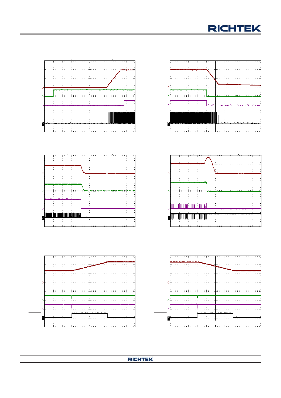
RT8885A
Typical Operating Characteristics
V
CORE
(500mV/Div)
EN
(2V/Div)
VR_READY
(2V/Div)
UGATE1
(20V/Div)
V
CORE
(1V/Div)
I
LOAD
(154A/Div)
CORE VR Power On from EN
Boot VID = 1V
Time (200μs/Div)
CORE VR OCP
V
CORE
(500mV/Div)
EN
(2V/Div)
VR_READY
(2V/Div)
UGATE1
(20V/Div)
V
CORE
(1V/Div)
VR_READY
(1V/Div)
CORE VR Power Off from EN
Boot VID = 1V
Time (200μs/Div)
CORE VR OVP and NVP
VR_READY
(1V/Div)
UGATE1
(50V/Div)
V
CORE
(500mV/Div)
VCLK
(2V/Div)
VDIO
(2V/Div)
ALERT
(2V/Div)
VID = 1.1V, I
LOAD(MAX) =
Time (100μs/Div)
CORE VR Dynamic VID Up
0.7V to 1.2V, Slew Rate = Slow, I
Time (40μs/Div)
LOAD =
123A
20A
UGATE1
(50V/Div)
LGATE1
(10V/Div)
V
CORE
(500mV/Div)
VCLK
(2V/Div)
VDI O
(2V/Div)
ALERT
(2V/Div)
VID = 1.1V
Time (40μs/Div)
CORE VR Dynamic VID Down
1.2V to 0.7V, Slew Rate = Slow, I
Time (40μs/Div)
LOAD =
20A
Copyright 2014 Richtek Technology Corporation. All rights reserved. is a registered trademark of Richtek Technology Corporation.
©
DS8885A-01 January 2014www.richtek.com
32
Page 33
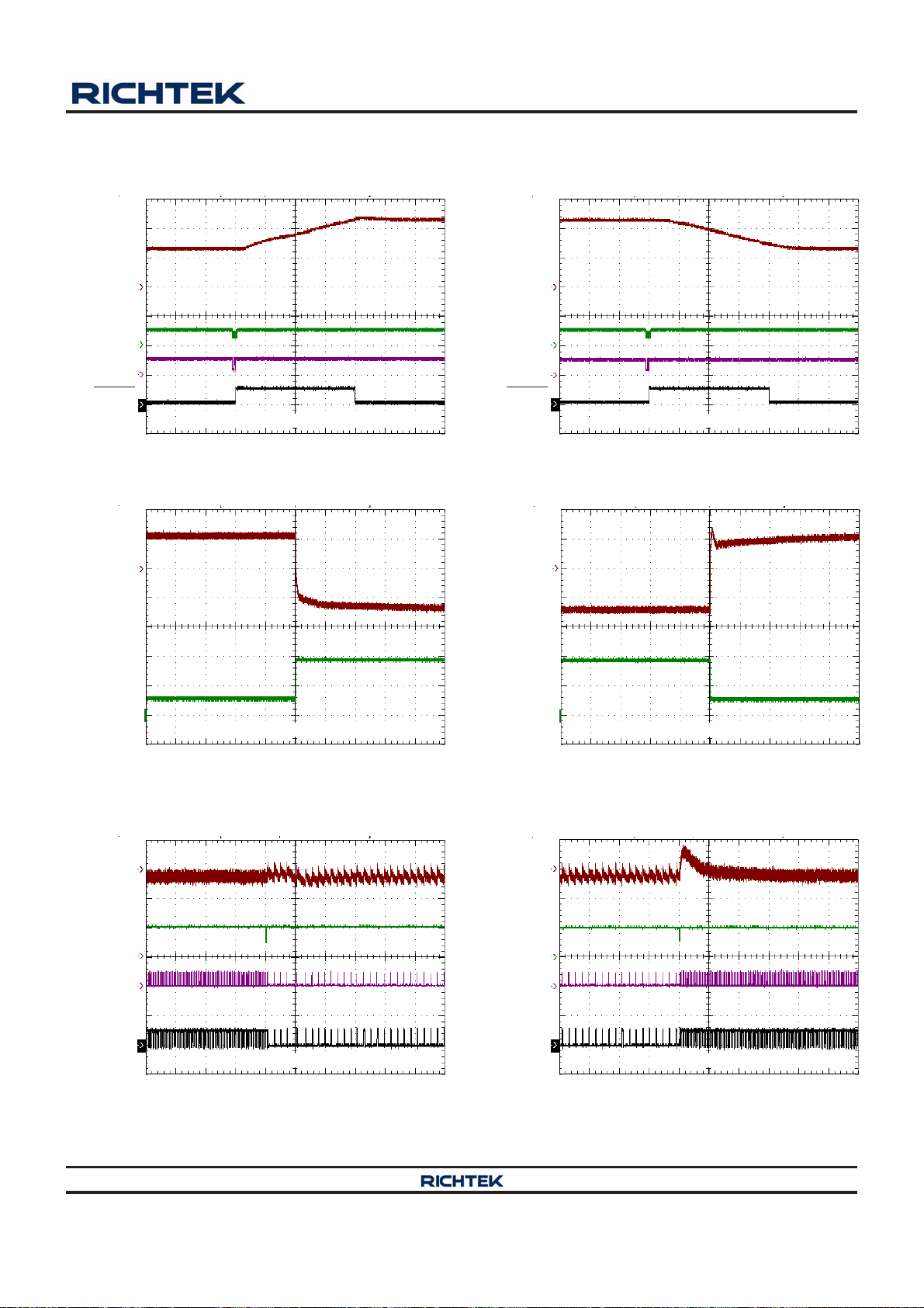
RT8885A
V
CORE
(500mV/Div)
VCLK
(2V/Div)
VDIO
(2V/Div)
ALERT
(2V/Div)
V
CORE
(50mV/Div)
CORE VR Dynamic VID Up
0.7V to 1.2V, Slew Rate = Fast, I
Time (10μs/Div)
LOAD =
CORE VR Load Transient
20A
V
CORE
(500mV/Div)
VCLK
(2V/Div)
VDIO
(2V/Div)
ALERT
(2V/Div)
V
CORE
(50mV/Div)
CORE VR Dynamic VID Down
1.2V to 0.7V, Slew Rate = Fast, I
Time (10μs/Div)
LOAD =
CORE VR Load Transient
20A
I
LOAD
(A/Div)
V
CORE
(20mV/Div)
VCLK
(1V/Div)
UGATE1
(50V/Div)
LGATE1
(10V/Div)
94
28
VID = 0.9V, f
= 305Hz, Rise Time = 150ns
LOAD
Time (100μs/Div)
CORE VR Mode Transient
VID = 1.1V, PS0 to PS2, I
Time (100μs/Div)
LOAD =
0.6A
I
LOAD
(A/Div)
V
CORE
(20mV/Div)
VCLK
(1V/Div)
UGATE1
(50V/Div)
LGATE1
(10V/Div)
94
28
VID = 0.9V, f
= 305Hz, Rise Time = 150ns
LOAD
Time (100μs/Div)
CORE VR Mode Transient
VID = 1.1V, PS2 to PS0, I
Time (100μs/Div)
LOAD =
0.6A
Copyright 2014 Richtek Technology Corporation. All rights reserved. is a registered trademark of Richtek Technology Corporation.
©
DS8885A-01 January 2014 www.richtek.com
33
Page 34

RT8885A
TSEN
(100mV/Div)
VRHOT
(500mV/Div)
V
GFX
(500mV/Div)
EN
(2V/Div)
VRA_READY
(2V/Div)
CORE VR Thermal Monitoring
Time (10ms/Div)
GFX VR Power On form EN
CORE VR Reference Voltage vs. Temperature
1.002
1.001
1.000
0.999
0.998
0.997
Reference Voltage (V)
0.996
0.995
-50 -25 0 25 50 75 100 125
Temp erature (° C)
GFX VR Power Off form EN
V
GFX
(500mV/Div)
EN
(2V/Div)
VRA_READY
(2V/Div)
VID = 1VTSEN Sweep from 1.7V to 1.9V
UGATE1
(20V/Div)
V
GFX
(1V/Div)
I
LOAD
(138A/Div)
VRA_READY
(1V/Div)
UGATE1
(50V/Div)
Time (200μs/Div)
GFX VR OCP
VID = 1.1V, I
Time (100μs/Div)
Boot VID = 1V
LOAD(MAX) =
55A
UGATE1
(20V/Div)
V
GFX
(1V/Div)
VRA_READY
(1V/Div)
UGATE1
(50V/Div)
LGATE1
(10V/Div)
Boot VID = 1V
Time (200μs/Div)
GFX VR OVP and NVP
VID = 1.1V
Time (40μs/Div)
Copyright 2014 Richtek Technology Corporation. All rights reserved. is a registered trademark of Richtek Technology Corporation.
©
DS8885A-01 January 2014www.richtek.com
34
Page 35
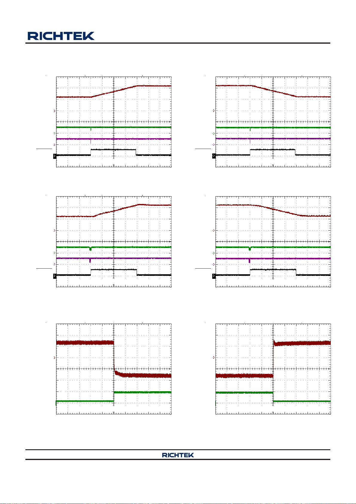
RT8885A
V
GFX
(500mV/Div)
VCLK
(2V/Div)
VDIO
(2V/Div)
ALERT
(2V/Div)
V
GFX
(500mV/Div)
GFX VR Dynamic VID Up
0.7V to 1.2V, Slew Rate = Slow, I
Time (40μs/Div)
GFX VR Dynamic VID Up
LOAD =
20A
V
GFX
(500mV/Div)
VCLK
(2V/Div)
VDIO
(2V/Div)
ALERT
(2V/Div)
V
GFX
(500mV/Div)
GFX VR Dynamic VID Down
1.2V to 0.7V, Slew Rate = Slow, I
Time (40μs/Div)
LOAD =
GFX VR Dynamic VID Down
20A
VCLK
(2V/Div)
VDIO
(2V/Div)
ALERT
(2V/Div)
V
GFX
(50mV/Div)
I
LOAD
(A/Div)
46
9
0.7V to 1.2V, Slew Rate = Fast, I
Time (10μs/Div)
GFX VR Load Transient
VID = 1.23V, f
= 305Hz, Rise Time = 150ns
LOAD
LOAD =
20A
VCLK
(2V/Div)
VDIO
(2V/Div)
ALERT
(2V/Div)
V
GFX
(50mV/Div)
I
LOAD
(A/Div)
46
9
1.2V to 0.7V, Slew Rate = Fast, I
Time (10μs/Div)
GFX VR Load Transient
VID = 1.23V, f
= 305Hz, Rise Time = 150ns
LOAD
LOAD =
20A
Time (100μs/Div)
Copyright 2014 Richtek Technology Corporation. All rights reserved. is a registered trademark of Richtek Technology Corporation.
©
Time (100μs/Div)
DS8885A-01 January 2014 www.richtek.com
35
Page 36
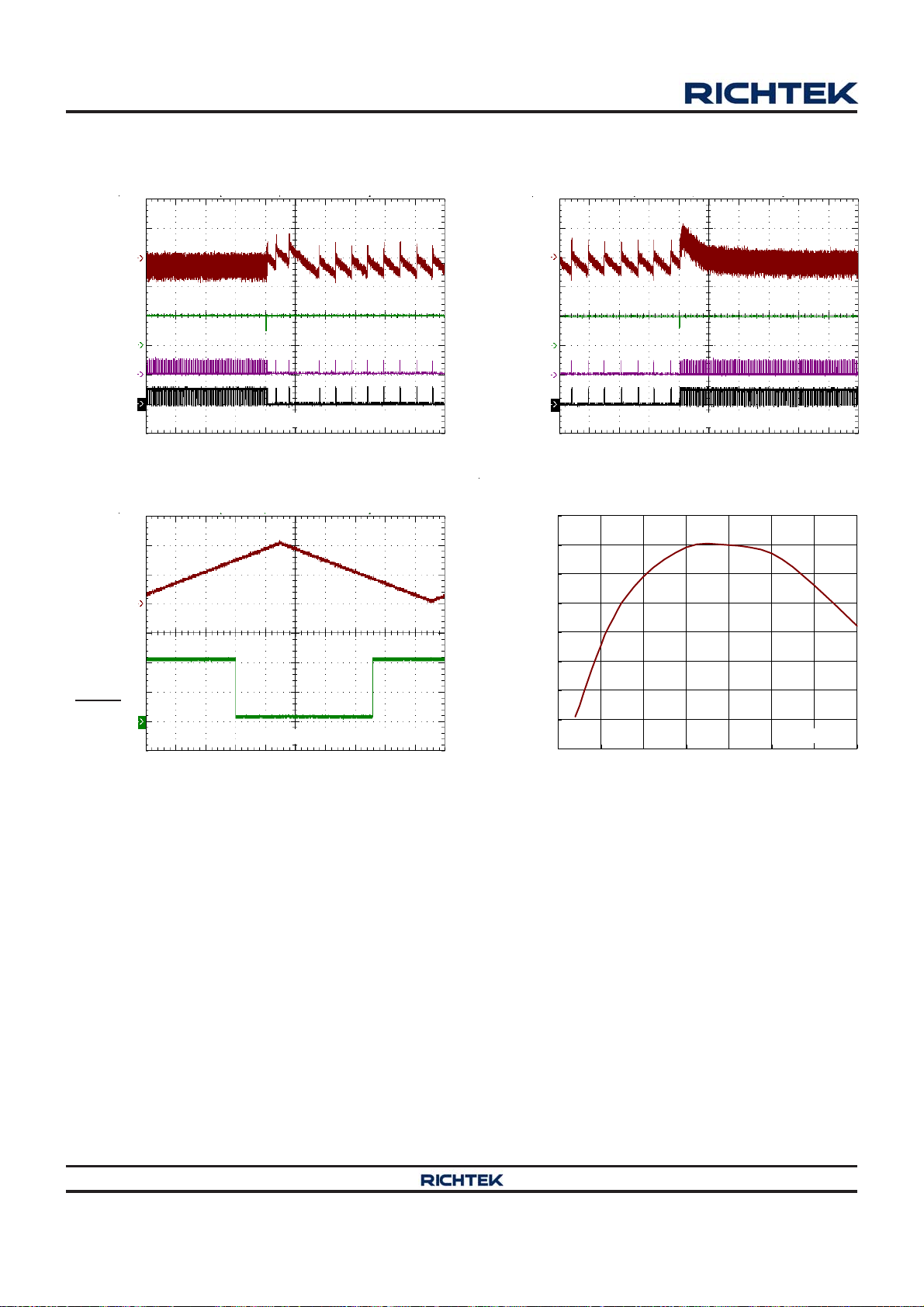
RT8885A
V
GFX
(20mV/Div)
VCLK
(1V/Div)
UGATE1
(50V/Div)
LGATE1
(10V/Div)
TSENA
(100mV/Div)
GFX VR Mode Transient
VID = 1.1V, PS0 to PS2, I
Time (100μs/Div)
LOAD =
GFX VR Thermal Monitoring
0.2A
GFX VR Mode Transient
V
GFX
(20mV/Div)
VCLK
(1V/Div)
UGATE1
(50V/Div)
LGATE1
(10V/Div)
VID = 1.1V, PS2 to PS0, I
Time (100μs/Div)
GFX VR Reference Voltage vs. Temperature
1.004
1.003
1.002
1.001
LOAD =
0.2A
VRHOT
(500mV/Div)
TSENA Sweep from 1.7V to 1.9V
Time (10ms/Div)
Reference Voltage (V)
1.000
0.999
0.998
0.997
VID = 1V
0.996
-50-25 0 25 50 75100125
Temperature (°C)
Copyright 2014 Richtek Technology Corporation. All rights reserved. is a registered trademark of Richtek Technology Corporation.
©
DS8885A-01 January 2014www.richtek.com
36
Page 37
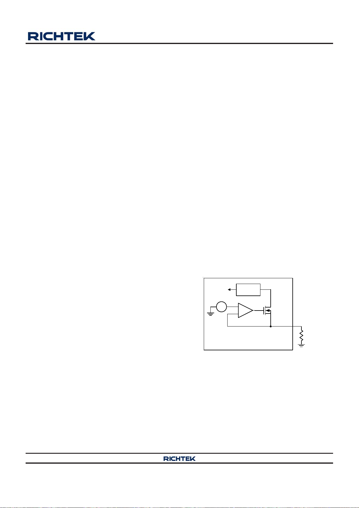
Application Information
RT8885A
The RT8885A is a CPU power controller which includes
two voltage rails : a 3/2/1 phase synchronous buck
controller, the CORE VR, and a 2/1 phase synchronous
buck controller, the GFX VR. The IC is compliant with
Intel VR12/IMVP7 voltage regulator specification to fulfill
Intel's CPU power supply requirements of both CORE and
GFX voltage rails. A Serial VID (SVID) interface is built-in
the RT8885A to communicate with Intel VR12/IMVP7
compliant CPU.
The RT8885A adopts G-NAVPTM (Green Native AVP), which
is Richtek's proprietary topology derived from finite DC
gain compensator with current mode control, making it
an easy setting PWM controller, meeting all Intel CPU
requirements of AVP (Active Voltage Positioning). The load
line can be easily programmed by setting the DC gain of
the error amplifier. The RT8885A has fast transient response
due to the G-NAVPTM commanding variable switching
frequency. Based on the G-NAVPTM topology, the IC also
features a quick response mechanism for optimized AVP
performance during load transient.
The G-NAVPTM topology also represents a high efficiency
system with green power concept. With the G-NAVP
TM
topology, the RT8885A becomes a green power controller
with high efficiency under heavy load, light load, and very
light load conditions. The IC supports mode transition
function with various operating states, including multi-
phase, single phase and diode emulation modes. These
different operating states allow the overall power control
system to have the lowest power loss. By utilizing the G-
NAVPTM topology, the operating frequency of the RT8885A
varies with VID, load, and input voltage to further enhance
the efficiency even in CCM.
The built-in high accuracy DAC converts the SVID code
ranging from 0.25V to 1.52V with 5mV per step. The
RT8885A supports VID on-the-fly function with three
different slew rates : Fast, Slow and Decay. The RT8885A
also built-in in a high accuracy ADC for some platform
setting functions, such as no-load offset or over current
level. The controller supports both DCR and sense resistor
current sensing. The RT8885A provides VR_READY and
VRA_READY signals for both CORE VR and GFX VR. It
also features complete fault protection function including
over voltage, under voltage, negative voltage, over current
and under voltage lockout. The RT8885A is available in a
WQFN-56L 7x7 small footprint package.
General Loop Functions :
Precise Reference Current Generation
The RT8885A includes complicated analog circuits inside
the controller. These analog circuits need very precise
reference voltage/current to drive these analog devices.
The RT8885A will auto generate a 2.14V voltage source
at IBIAS pin, and an exact 53.6kΩ resistor is required to
be connected between IBIAS and analog ground, as shown
in Figure 1. Through this connection, the RT8885A will
generate a 40μA current from the IBIAS pin to analog
ground, and this 40μA current will be mirrored inside the
RT8885A for internal use. Note that other type of
connection or other values of resistance applied at the
IBIAS pin may cause failure of the RT8885A's functions,
such as slew rate control, OFS accuracy, etc. In other
words, the IBIAS pin can only be connected with an exact
53.6kΩ resistor to GND. The resistance accuracy of this
resistor is recommended to be 1% or higher.
Current
Mirror
2.14V
+
-
+
-
IBIAS
53.6k
Figure 1. IBIAS Setting
SET1 Pin Setting
The RT8885A provides SET1 pin for platform users to set
CORE VR's functions : initial startup voltage V
INI_CORE
maximum output current ICCMAX and PWM on-time of
quick response for load transient boost.
Figure 2 (a) shows PWM on-time of quick response QR
for CORE VR setting with the SET1 pin voltage V
SET1_DIV
When EN pin goes high, the SET1 pin voltage is sensed
,
.
Copyright 2014 Richtek Technology Corporation. All rights reserved. is a registered trademark of Richtek Technology Corporation.
DS8885A-01 January 2014 www.richtek.com
©
37
Page 38
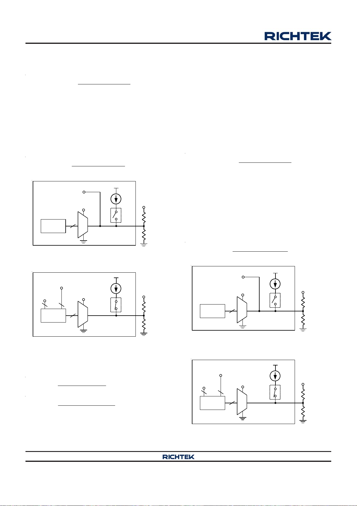
RT8885A
and held to set PWM on-time of quick response for load
transient boost. The SET1 pin voltage V
SET1_DIV
is shown
as :
R
VVCC
SET1_DIV
RR
Figure 2 (b) shows V
setting with the SET1 pin voltage differenceΔV
SET1_D
SET1_U SET1_D
INI_CORE
and ICCMAX for CORE VR
SET1
(1)
. After
PWM on-time of QR for CORE VR setting, a 40μA is
injected into SET1 pin while the SET1 pin voltage difference
ΔV
is sensed and decoded to set initial startup voltage
SET1
V
INI_CORE
SET1 pin voltage difference ΔV
V40A
and maximum output current ICCMAX. The
is shown as :
SET1
V
SET1_DIV
ADC
40µA
SET1
SET1
QR On-time
V
SET1
Register
RR
SET1_U SET1_D
RR
SET1_U SET1_D
2.24V
VCC
R
SET1_U
R
SET1_D
(2)
SET2 Pin Setting
The RT8885A provides SET2 pin for platform users to set
GFX VR's functions : initial startup voltage V
INI_GFX
maximum output current ICCMAXA and PWM on-time of
quick response for load transient boost.
Figure 3 (a) shows PWM on-time of quick response QR
for GFX VR setting with the SET2 pin voltage V
SET2_DIV
When EN pin goes high, the SET2 pin voltage is sensed
and held to set PWM on-time of quick response for load
transient boost. The SET2 pin voltage V
SET2_DIV
is shown
as :
R
VVCC
SET2_DIV
RR
Figure 3 (b) shows V
setting with the SET2 pin voltage difference ΔV
SET2_D
SET2_U SET2_D
INI_GFX
and ICCMAXA for GFX VR
SET2
(5)
. After
PWM on-time of QR for GFX VR setting, a 40μA is injected
into SET2 pin while the SET2 pin voltage difference ΔV
is sensed and decoded to set initial startup voltage V
SET2
INI_GFX
and maximum output current ICCMAXA. The SET2 pin
voltage difference ΔV
is shown as :
SET2
,
.
Figure 2 (a). PWM On-Time of Quick Response for
CORE VR Setting
V
INI_CORE
(2-bits)
ICCMAX
(4-bits)
V
SET1
Register
Figure 2 (b). V
2.24V
ADC
INI_CORE
40µA
VCC
R
V
SET1
SET1
SET1_U
R
SET1_D
and ICCMAX for CORE VR
Setting
If V
SET1_DIV
and ΔV
are determined, R
SET1
SET1_U
and R
SET1_D
can be calculated as follows :
R =
SET1_U
R =
SET1_D
VCC V
40 A V
RV
SET1_U SET1_ DIV
VCC V
SET1
SET1_DIV
SET1_DIV
(3)
(4)
In addition, Richtek provides a Microsoft Excel-based
spreadsheet to help design the SET1 resistor network for
CORE VR.
V
SET2_DIV
ADC
R
SET2_U
R
SET2_D
(6)
40µA
VCC
SET2
RR
V40A
SET2
QR On-time
V
SET2
Register
SET2 _U SET2 _D
RR
SET2 _U SET2 _D
2.24V
Figure 3 (a). PWM On-Time of Quick Response for GFX
VR Setting
V
ICCMAXA
(4-bits)
V
SET2
Register
Figure 3 (b). V
INI_GFX
(2-bits)
2.24V
V
SET2
ADC
and ICCMAXA for GFX VR Setting
INI_GFX
40µA
SET2
VCC
R
SET2_U
R
SET2_D
Copyright 2014 Richtek Technology Corporation. All rights reserved. is a registered trademark of Richtek Technology Corporation.
©
DS8885A-01 January 2014www.richtek.com
38
Page 39

RT8885A
If V
SET2_DIV
and ΔV
are determined, R
SET2
SET2_U
and R
SET2_D
can be calculated as follows :
R =
SET2 _U
R =
SET2 _D
VCC V
40 A V
RV
SET2 _U SET2 _ DIV
VCC V
SET2
SET2 _ DIV
SET2 _ DIV
(7)
(8)
In addition, Richtek provides a Microsoft Excel-based
spreadsheet to help design the SET2 resistor network for
GFX VR.
RSET/OFS Pin Setting
The RT8885A provides RSET/OFS pin for platform users
to set CORE VR's functions : internal compensation ramp
factor for control loop, output voltage offset and forced-
DEM operation.
Figure 4 (a) shows output voltage offset for CORE VR
setting with the RSET/OFS pin voltage V
RSET_DIV
. When
EN pin goes high, the RSET/OFS pin voltage is sensed
and held to set output voltage offset for CORE VR. The
RSET/OFS pin voltage V
VVCC
RSET _DIV
RSET_DIV
RR
RSET_U RSET_D
R
RSET_D
is shown as :
(9)
Figure 4 (b) shows internal compensation ramp factor and
forced-DEM operation for CORE VR setting with the
RSET/OFS pin voltage difference ΔV
. After output
RSET
voltage offset for CORE VR setting, a 40μA is injected
into RSET/OFS pin while the RSET/OFS pin voltage
difference ΔV
is sensed and decoded to set internal
RSET
compensation ramp factor and forced-DEM operation. The
RSET/OFS pin voltage difference ΔV
V
RSET_DIV
ADC
RR
V40A
RSET
QR On-time
V
RSET
Register
RSET _U RSET _D
RR
RSET _U RSET _ D
2.24V
RSET
40µA
RSET
is shown as :
(10)
VCC
R
RSET_U
R
RSET_D
Figure 4 (a). Output Voltage Offset for CORE VR Setting
Forced-DEM
(1-bits)
Ramp Current
(5-bits)
V
RSET
Register
2.24V
ADC
V
RSET
40µA
RSET
VCC
R
RSET_U
R
RSET_D
Figure 4 (b). Internal Compensation Ramp Factor and
Forced-DEM Operation for CORE VR Setting
If V
RSET_DIV
R
RSET_D
R =
RSET _ U
R =
RSET _ D
and ΔV
are determined, R
RSET
can be calculated as follows :
VCC V
40 A V
RV
RSET _U RSET _DIV
VCC V
RSET
RSET _ DIV
RSET _ DIV
RSET_U
and
(11)
(12)
In addition, Richtek provides a Microsoft Excel-based
spreadsheet to help design the RSET/OFS resistor
network for CORE VR.
RSET A/OFSA Pin Setting
The RT8885A provides RSETA/OFSA pin for platform users
to set GFX VR's functions : internal compensation ramp
factor for control loop, output voltage offset and forced-
DEM operation.
Figure 5 (a) shows output voltage offset for GFX VR setting
with the RSETA/OFSA pin voltage V
RSETA_DIV
. When EN
pin goes high, the RSETA/OFSA pin voltage is sensed
and held to set output voltage offset for GFX VR. The
RSETA/OFSA pin voltage V
VVCC
RSETA_DIV
RSETA_DIV
R
RR
RSETA_U RSETA_D
RSETA_D
is shown as :
(13)
Figure 5 (b) shows internal compensation ramp factor and
forced-DEM operation for GFX VR setting with the RSETA/
OFSA pin voltage difference ΔV
. After output voltage
RSETA
offset for GFX VR setting, a 40μA is injected into RSETA/
OFSA pin while the RSETA/OFSA pin voltage difference
ΔV
is sensed and decoded to set internal
RSETA
compensation ramp factor and forced-DEM operation. The
RSETA/OFSA pin voltage difference ΔV
RR
V40A
RSETA
RSETA _ U RSETA _D
RR
RSETA _U RSETA _ D
is shown as:
RSETA
(14)
Copyright 2014 Richtek Technology Corporation. All rights reserved. is a registered trademark of Richtek Technology Corporation.
DS8885A-01 January 2014 www.richtek.com
©
39
Page 40
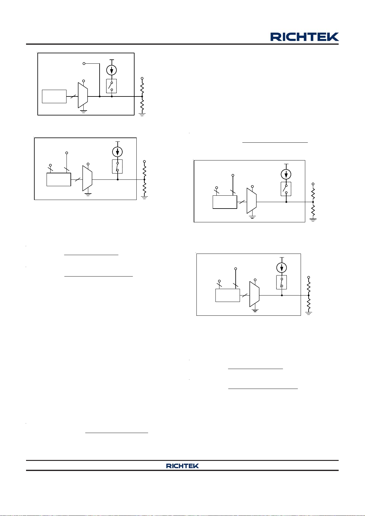
RT8885A
QR On-time
V
RSETA
Register
RSETA_DIV
2.24V
ADC
40µA
RSETA
VCC
R
RSETA_U
R
RSETA_D
V
Figure 5 (a). Output Voltage Offset for GFX VR Setting
Forced-DEM
(1-bits)
Ramp Current
(5-bits)
V
RSETA
Register
2.24V
ADC
V
RSETA
40µA
RSETA
VCC
R
RSETA_U
R
RSETA_D
Figure 5 (b). Internal Compensation Ramp Factor and
Forced-DEM Operation for GFX VR Setting
If V
RSETA_DIV
R
RSETA_D
R =
RSETA _U
R =
RSETA _D
and ΔV
are determined, R
RSETA
can be calculated as follows :
VCC V
40 A V
RV
RSETA _U RSETA _DIV
VCC V
RSETA
RSETA _DIV
RSETA _DIV
RSETA_U
and
(15)
(16)
In addition, Richtek provides a Microsoft Excel-based
spreadsheet to help design the RSETA/OFSA resistor
network for GFX VR.
Figure 6 (b) shows GFX VR's summed total over current
protection SUM_OCP threshold and per phase over current
protection PH_OCP threshold setting with the OCSET
pin voltage difference ΔV
. After CORE VR over current
OCSET
protection thresholds setting, a 40μA is injected into
OCSET pin while the OCSET pin voltage difference
ΔV
is sensed and decoded to set SUM_OCP and
OCSET
PH_OCP thresholds for GFX VR. The OCSET pin voltage
difference ΔV
V40A
OCSET
CORE Summed
OCP (3-bits)
CORE Per-phase
OCP (3-bits)
V
OCSET
Register
is shown as :
OCSET
V
OCSET_DIV
RR
OCSET _U OCSET _ D
RR
OCSET _ U OCSET _ D
2.24V
ADC
40µA
OCSET
VCC
R
OCSET_U
R
OCSET_D
(18)
Figure 6 (a). CORE VR SUM_OCP and PH_OCP
Thresholds Setting
GFX Summed
OCP (3-bits)
GFX Per-phase
OCP (3-bits)
V
OCSET
Register
2.24V
V
ADC
OCSET
40µA
OCSET
VCC
R
OCSET_U
R
OCSET_D
OCSET Pin Setting
The RT8885A provides OCSET pin for platform users to
set CORE VR and GFX VR over current protection
thresholds.
Figure 6 (a) shows CORE VR's summed total over current
protection SUM_OCP threshold and per phase over current
protection PH_OCP threshold setting with the OCSET
pin voltage V
OCSET_DIV
. When EN pin goes high, the OCSET
pin voltage is sensed, held and decoded to set SUM_OCP
and PH_OCP thresholds for CORE VR. The OCSET pin
voltage V
VVCC
OCSET_DIV
Copyright 2014 Richtek Technology Corporation. All rights reserved. is a registered trademark of Richtek Technology Corporation.
OCSET_DIV
©
is shown as :
R
OCSET_D
RR
OCSET_U OCSET_D
(17)
Figure 6 (b). GFX VR SUM_OCP and PH_OCP
Thresholds Setting
If V
OCSET_DIV
R
OCSET_D
R =
OCSET _ U
R =
OCSET _D
and ΔV
are determined, R
OCSET
can be calculated as follows :
VCC V
40 A V
RV
OCSET _U OCSET _ DIV
VCC V
OCSET
OCSET _DIV
OCSET _ DIV
OCSET_U
In addition, Richtek provides a Microsoft Excel-based
spreadsheet to help design the OCSET resistor network
for both VRs.
DS8885A-01 January 2014www.richtek.com
40
and
(19)
(20)
Page 41
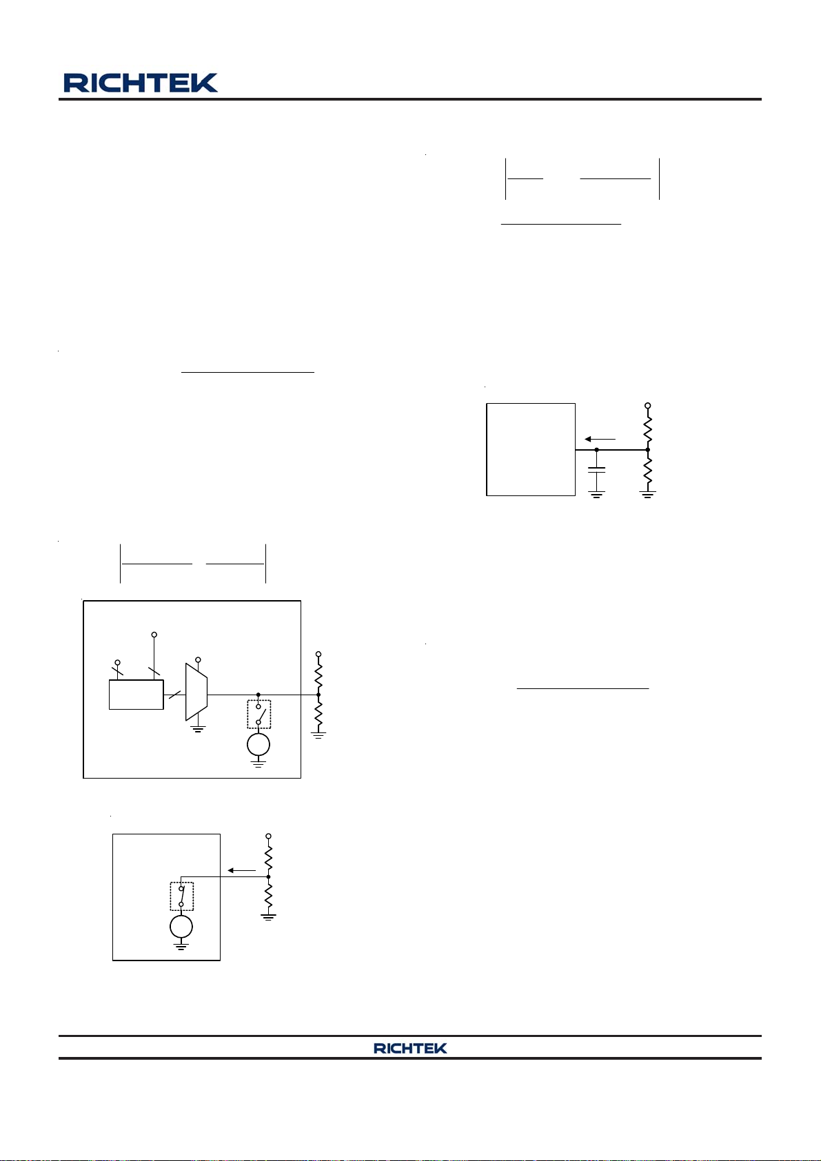
RT8885A
VREF/QRTH Pin Setting
The VREF/QRTH pin provides two functions: providing fixed
0.6V reference voltage output during normal operation of
VR controller and programming the quick response trigger
thresholds (QRTH) for CORE VR and GFX VR.
Figure 7 (a) shows CORE VR and GFX VR QRTH setting
with the VREF/QRTH pin voltage V
QRTH_DIV
. When the
rising edge of EN pin goes high, the VREF/QRTH pin
voltage V
QRTH_DIV
is sensed and decoded to set QRTH for
CORE VR and GFX VR. The VREF/QRTH pin voltage
V
QRTH_DIV
VV
QRTH_DIV
is shown as :
CC
RR
R
QRTH_ D
QRTH_ U QRTH _ D
(21)
Figure 7 (b) shows the illustration of 0.6V regulation at
the VREF/QRTH pin during the normal operation of VR
controller after EN pin goes high. Due to the design margin
of the internal voltage regulator, the sink current through
the VREF/QRTH pin should be under 300μA and source
current through the VREF/QRTH pin should be under
80μA.
V0.6V
I
VREF
CORE QRTH
OCP (3-bits)
Register
CC
RR
QRTH_U QRTH_D
CORE QRTH
OCP (3-bits)
V
QRTH
2.24V
V
ADC
Regulator
0.6V
QRTH_DIV
Voltage
+
-
VREF
0.6V
(22)
V
CC
R
QRTH_U
R
QRTH_D
If V
QRTH_DIV
and I
are determined, R
VREF
QRTH_U
and R
QRTH_D
can be calculated as follows :
R = 1
QRTH _ U
R = R
QRTH _ D QRTH _ U
V
IV
VREF QRTH_ DIV
VV
In the application circuit, the C
CC
0.6V
V
QRTH _ DIV
CC QRTH _ DIV
is used to stabilize
VREF
(23)
(24)
the internal voltage regulator at VREF/QRTH pin, as in
shown Figure 8. Therefore, the capacitance of C
VREF
must
be greater than 0.1μF and the maximum capacitance of
this capacitor is 2.2μF. However, this capacitance should
be chosen carefully due to the pin setting accuracy.
VCC
I
VREF
VREF/QRTH
C
Figure 8. Illustration of Capacitor C
VREF
R
QRTH_U
R
QRTH_D
at VREF/QRTH
VREF
Pin
In order to ensure the voltage on VREF/QRTH pin has
been settled when the rising edge of EN pin goes high
for pin setting accuracy, the equivalent RC time constant
at this pin should be under 2ms as shown in follows :
5R C 2ms
QUTH_ EQU VREF
VR
R =
QRTH _ EQU
QRTH_ U QRTH_ D
VR
QRTH_ U QRTH_ D
(25)
(26)
In addition, Richtek provides a Microsoft Excel-based
spreadsheet to help design the VREF/QRTH resistor
network for both VRs.
Figure 7 (a). CORE VR and GFX VR QRTH Setting
V
CC
R
QRTH_U
R
QRTH_D
Voltage
Regulator
VREF
+
-
0.6V
I
VREF
TSEN/ZLL Pin Setting
The TSEN/ZLL pin provides two functions for CORE VR :
thermal monitor input, and droop enable/disable setting.
Figure 9 (a) shows CORE VR droop enable/disable setting
with the TSEN/ZLL pin voltage difference ΔV
TSEN
. When
EN pin goes high, a 40μA is injected into TSEN/ZLL pin. If
the TSEN/ZLL pin voltage difference ΔV
is greater than
TSEN
3.8V, CORE VR droop is disabled. If not CORE VR droop
Figure 7 (b). Illustration of 0.6V Regulation at VREF Pin
Copyright 2014 Richtek Technology Corporation. All rights reserved. is a registered trademark of Richtek Technology Corporation.
DS8885A-01 January 2014 www.richtek.com
©
41
Page 42

RT8885A
is enabled. The TSEN/ZLL pin voltage difference ΔV
TSEN
is shown as :
RR
V40A
TSEN
where R
TSEN_EQU
TSEN _ 3 TSEN _EQU
RR
TSEN _ 3 TSEN _ EQU
R
RR
TSEN _ 1 TSEN_NTC
RR
TSEN_1 TSEN_ NTC
TSEN_ 2
(27)
Figure 9 (b) shows CORE VR thermal monitor function
enable/disable setting with the TSEN/ZLL pin voltage
V
TSEN_DIV
the TSEN/ZLL pin voltage V
the TSEN/ZLL pin voltage V
. After CORE VR droop enable/disable setting,
TSEN_DIV
TSEN_DIV
is sensed and held. If
is greater than 2.9V,
CORE VR thermal monitor function is disabled. If not
CORE VR thermal monitor function is enabled. The TSEN/
ZLL pin voltage V
VVCC
TSEN_DIV
TSEN_DIV
is shown as :
R
TSEN_3
RR
TSEN_3 TSEN_EQU
(28)
TSENA/ZLLA Pin Setting
The TSENA/ZLLA pin provides two functions for GFX VR :
thermal monitor input, and droop enable/disable setting.
Figure 10 (a) shows GFX VR droop enable/disable setting
with the TSENA/ZLLA pin voltage difference ΔV
TSENA
EN pin goes high, a 40μA is injected into TSENA/ZLLA
pin. If the TSENA/ZLLA pin voltage difference ΔV
greater than 3.8V, GFX VR droop is disabled. If not GFX
VR droop is enabled. The TSENA/ZLLA pin voltage
difference ΔV
V40A
TSENA
where R
TSENA_EQU
R
is shown as :
TSENA
RR
TSENA _3 TSENA _ EQU
RR
TSENA _3 TSENA _EQU
RR
TSENA _1 TSENA _ NTC
RR
TSENA _ 1 TSENA _NTC
TSENA _ 2
Figure 10 (b) shows GFX VR thermal monitor function
enable/disable setting with the TSENA/ZLLA pin voltage
VCC
40µA
TSEN
R
TSEN_1
R
TSEN_NTC
R
TSEN_2
R
TSEN_3
3.8V
Zero LL
CMP
+
-
+
-
V
TSEN_INJ
Figure 9 (a). CORE VR Droop Enable/Disable Setting
VCC
Disable TSEN
CMP
-
+
2.9V
-
+
V
TSEN_DIV
40µA
TSEN
R
TSEN_1
R
TSEN_NTC
R
TSEN_2
R
TSEN_3
V
TSENA_DIV
the TSENA/ZLLA pin voltage V
held. If the TSENA/ZLLA pin voltage V
. After GFX VR droop enable/disable setting,
TSENA_DIV
is sensed and
TSENA_DIV
is greater
than 2.9V, GFX VR thermal monitor function is disabled.
If not GFX VR thermal monitor function is enabled. The
TSENA/ZLLA pin voltage V
VVCC
TSENA_DIV
Zero LL
CMP
+
-
+
V
TSENA_INJ
-
3.8V
TSENA_DIV
RR
TSENA_3 TSENA_EQU
40µA
TSENA
R
TSENA_3
R
TSENA_1
is shown as :
VCC
R
R
TSENA_2
R
TSENA_3
Figure 10 (a). GFX VR Droop Enable/Disable Setting
Figure 9 (b). CORE VR Thermal Monitor Function
Enable/Disable Setting
If V
TSEN_DIV
R
TSEN_3
R =
TSEN_ EQU
R =
TSEN_ 3
and ΔV
are determined, R
TSEN
can be calculated as follows :
VCC V
40 A V
RV
TSEN_EQU TSEN_ DIV
VCC V
TSEN_ DIV
TSEN_DIV
TSEN
TSEN_EQU
and
(29)
(30)
40µA
R
Disable TSENA
CMP
+
-
+
2.9V
V
-
TSENA
TSENA_DIV
TSENA_1
Figure 10 (b). GFX VR Thermal Monitor Function Enable/
VCC
R
R
TSENA_2
R
TSENA_3
Disable Setting
Copyright 2014 Richtek Technology Corporation. All rights reserved. is a registered trademark of Richtek Technology Corporation.
42
©
DS8885A-01 January 2014www.richtek.com
. When
is
TSENA
(31)
(32)
TSENA_NTC
TSENA_NTC
Page 43

RT8885A
If V
TSENA_DIV
R
TSENA_3
R =
TSENA _EQU
R =
TSENA _ 3
V
INITA L
and ΔV
are determined, R
TSENA
can be calculated as follows :
VCC V
40 A V
RV
TSENA _EQU TSENA _ DIV
VCC V
TSENA
TSENA _DIV
TSENA _DIV
Setting
TSENA_EQU
and
(33)
(34)
The initial startup voltage of the RT8885A can be set by
platform users through the SET1 and the SET2 pins. Refer
to the SET1 and SET2 pin setting section and Table 3 and
Table 4, platform users can set the V
For example, choose VCC = 5V, V
= 53A and T
:
R
SET1_U
377.34k
R
SET1_D
32.81k
= TON, then solve for R
ON_QR
VCC V
40 A V
5V 1207.5mV
40 A 0.4V
VV
SET1_U SET1_ DIV
VCC V
377.34k 0.4V
5V 0.4V
SET1
SET1_DIV
SET1_DIV
INI_CORE
INI_CORE
and V
INI_GFX
= 1V, ICCMAX
and R
SET1_U
SET1_D
(35)
(36)
Start-Up Sequence
The RT8885A utilizes an internal soft-start sequence which
strictly follows Intel VR12/IMVP7 start-up sequence
specifications. After POR and EN go high, the controller
considers all the power inputs ready and enters start-up
sequence. If V
INITAL
= 0V, V
is programmed to stay at
OUT
0V for 2ms waiting for SVID command as shown in Figure
11 (a). If V
INITAL
0V, V
will ramp up to V
OUT
(which is not zero) immediately after both POR go high
and EN go high as shown in Figure 11 (b). After V
reaches target V
.
SVID command. After the RT8885A receives a valid VID
INITAL
, V
OUT
will stay at V
INITAL
code (typically SetVID_Slow command), V
up to the target voltage with specified slew rate (see
section “Data and Configuration Register”). After V
reaches target voltage (VID voltage for V
for V
INITAL
0), the RT8885A will send out VR_READY
INITAL
signal to indicate that the power state of the RT8885A is
ready. The VR ready circuit is an open-drain structure, so
a pull-up resistor connected to a voltage source is required.
voltage
INITAL
waiting for
will ramp
OUT
= 0 or V
OUT
OUT
INITAL
VCC
POR
EN
SVID
V
OUT_CORE
PWM
V
OUT_GFX
PWMA
VR_READY
VRA_READY
4.2V
T
= 2ms (MAX)
SET
XX
Hi-Z
Hi-Z
SVID
MAX Phases
Valid
Defined
SVID
MAX Phases
100µs
SVID
SVID
Defined
100µs
MAX Phases
MAX Phases
Figure 11 (a). Power Sequence for the RT8885A (V
SVID
SVID
INITIAL
0.2V
0.2V
= V
Hi-Z
Hi-Z
INITIALA
4.1V
XX
= 0V)
Copyright 2014 Richtek Technology Corporation. All rights reserved. is a registered trademark of Richtek Technology Corporation.
©
DS8885A-01 January 2014 www.richtek.com
43
Page 44

RT8885A
VCC
POR
EN
SVID
V
OUT_CORE
PWM
V
OUT_GFX
PWMA
VR_READY
VRA_READY
4.2V
T
= 2ms (MAX)
SET
XX
Hi-Z
Hi-Z
SVID
Defined
SVID
MAX Phases
Valid XX
VBOOT
SVID
Defined
VBOOTA
SVID
Defined
100µs
100µs
SVID
MAX Phases
SVID
MAX Phases
SVID
Defined
Defined
Figure 11 (b). Power Sequence for the RT8885A (V
SVID
INITIAL
SVID
MAX Phases
SVID
MAX Phases
0V, V
0.2V
0.2V
INITIALA
4.1V
Hi-Z
Hi-Z
0V)
Power Down Sequence
Similar to the start-up sequence, the RT8885A also utilizes
a soft shutdown mechanism during turn-off. After EN goes
low, the internal reference voltage (positive terminal of
compensation EA) starts ramping down with 3.125mV/μs
slew rate, and V
After V
drops below 0.2V, the RT8885A will be shut
OUT
will follow the reference voltage to 0V.
OUT
down and all functions (drivers) are disabled. The
VR_READY and VRA_READY will be pulled down
immediately after POR goes low or EN goes low.
CORE VR
Active Phase Determination : Before EN
The number of active phases is determined by the internal
circuitry that monitors the ISENxN voltages during start-
up. Normally, the CORE VR operates as a 3-phase PWM
controller. Setting ISEN3N to VCC before power on can
program a 2-phase operation, and pulling ISEN2N, and
setting ISEN2N, and ISEN3N to VCC before power on can
program a 1-phase operation. Before EN, CORE VR
detects whether the voltages of ISEN2N and ISEN3N are
higher than “VCC − 0.5V” respectively to decide how
many phases should be active. Phase selection is only
active during EN. When EN = high, the number of active
phases is determined and latched. The unused ISENxP
pins are recommended to be connected to VCC and
unused PWM pins can be left floating.
Loop Control
The CORE VR adopts Richtek's proprietary G-NAVP
TM
topology. G-NAVPTM is based on the finite gain peak current
mode with CCRCOT (Constant Current Ripple Constant
On-Time) topology. The output voltage, V
OUT_CORE
will
decrease with increasing output load current. The control
loop consists of PWM modulators with power stages,
current sense amplifiers and an error amplifier as shown
in Figure 12.
Similar to the peak current mode control with finite
compensator gain, the HS_FET on-time is determined by
CCRCOT on-time generator. When load current increases,
VCS increases, the steady state COMP voltage also
increases and induces V
OUT_CORE
to decrease, thus
achieving AVP. A near-DC offset canceling is added to the
output of EA to eliminate the inherent output offset of finite
gain peak current mode controller.
Copyright 2014 Richtek Technology Corporation. All rights reserved. is a registered trademark of Richtek Technology Corporation.
©
DS8885A-01 January 2014www.richtek.com
44
Page 45

V
IN
CMP
V
SS_SENSE
HS_FET
LS_FET
R
CSx
C2 C1
R2
R
R1
CCRCOT
PWM
+
COMP2
Logic
-
V
CS
1/3
-
EA
+
GM
PWMx
ISENxP
+
ISENxN
-
IMON
VREF
COMP
+
RGND
-
V
DAC
FB
Driver
R
IMON
V
R
SENSE
C
OUT_CORE
X
V
CC_SENSE
R
C
L
X
Figure 12. CORE VR : Simplified Schematic for Droop
and Remote Sense in CCM
TON Setting
High frequency operation optimizes the application for the
smaller component size, trading off efficiency due to higher
switching losses. This may be acceptable in ultra portable
devices where the load currents are lower and the
controller is powered from a lower voltage supply. Low
frequency operation offers the best overall efficiency at
the expense of component size and board space. Figure
13 shows the On-Time setting Circuit. Connect a resistor
(R
) between V
TON
IN_CORE
and TONSET to set the on-time
of UGATE :
12
t (0.5VV 1.2V)
ON DAC
24.4 10 R
VV
IN DAC
where tON is the UGATE turn on period, V
input voltage of the CORE VR, and V
is the DAC voltage.
DAC
TON
IN_CORE
(37)
is the
RT8885A
avoid this disadvantage of CCRCOT topology. When V
is larger than 1.2V, the on-time equation will be modified
to :
C
t (V 1.2V)
ON DAC
20.33 10 R V
VV
IN DAC
TON DAC
12
On-time translates only roughly to switching frequencies.
For better efficiency of the given load range, the maximum
switching frequency is suggested to be :
f
SW(MAX)
where f
V
mode or HFM, V
(t 60ns) R 50ns
ON ON _ LS FET(MAX)
IccTDC
VDCRRNR
DAC _ PS0 ON _ LS FET(MAX) DROOP
VRR
IN(MAX) ON _ LS FET(MAX) ON_ HS FET(MAX )
DAC_PS0
N
ITDC
CC
N
is the maximum switching frequency,
S(MAX)
is the test VID of application at PS0 for turbo
IN(MAX)
IccTDC
is the maximum application input
1
N
voltage, IccTDC is the thermal design current of application,
N is the phase number, R
equivalent high side FET R
ON_HS-FET(MAX)
DS(ON)
maximum equivalent low side FET R
inductor DCR, and R
is the load line setting.
DROOP
is the maximum
, R
ON_LS-FET(MAX)
DS(ON)
, DCR is the
Current Sense Setting
The current sense topology of the CORE VR is continuous
inductor current sensing. Therefore, the controller has less
noise sensitive. Low offset amplifiers are used for current
balance, loop control and over current detection. The
ISENxP and ISENxN pins denote the positive and negative
input of the current sense amplifier of each phase.
DAC
(38)
(39)
is the
Users can either use a current sense resistor or the
CCRCOT
On-Time
Computer
On-Time
TONSET
V
DAC
R
Figure 13. CORE VR : On-Time Setting with RC Filter
When V
is larger than 1.2V, the equivalent switching
DAC
frequency may be over 500kHz, and this too fast switching
TON
R1
C1
V
IN_CORE
inductor's DCR for current sensing. Using the inductor’s
DCR allows higher efficiency as shown in Figure 14.
V
L
CSx
OUT_CORE
DCR
C
X
I
SENxN
+
-
ISENxP
ISENxN
I
L
R
X
R
frequency is unacceptable. Therefore, the CORE VR
implements a pseudo constant frequency technology to
Copyright 2014 Richtek Technology Corporation. All rights reserved. is a registered trademark of Richtek Technology Corporation.
DS8885A-01 January 2014 www.richtek.com
©
Figure 14. CORE VR : Lossless Inductor Sensing
45
Page 46

RT8885A
In order to optimize transient performance, RX and CX must
be set according to the equation below :
L
DCR
RC
X
X
(40)
Then the proportion between the phase current IL and the
sensed current I
DCR
II
where R
SENxN L
R
only an exact 680Ω sense resistor. The
CSx
resistance accuracy of R
can be described as below :
SENxN
CSx
is recommended to be 1% or
CSx
(41)
higher.
In addition to considering the inductance tolerance, the
resistor RX has to be tuned on board by examining the
transient voltage. If the output voltage transient has an
initial dip below the minimum load line requirement and
the recovery is too fast causing a ring back. Vice versa,
with a resistance too large the output voltage transient
has only a small initial dip with a slow recovery.
Using current sense resistor in series with the inductor
can have better accuracy, but the efficiency is a trade-off.
Considering the equivalent inductance (L
) of the current
ESL
sense resistor, an RC filter is recommended. The RC filter
calculation method is similar to the above mentioned
inductor DCR sensing method.
Current Monitoring and Current Reporting
The RT8885A provides the current monitor function for
CORE VR. IMON pin reports CORE VR inductor current.
The IMON pin outputs a high-speed analog current source
that is 1 time of the summed current. Thus I
IMON
can be
described as below :
II
IMON SENxN
(42)
The RT8885A monitors the IMON pin voltage and considers
that CORE VR has reached ICCMAX when IMON pin
voltage is 2.392V.
As Figure 12 shows, a resistor R
the IMON pin and VREF pin. Through the R
is connected between
IMON
to convert
IMON
the IMON pin current to voltage. The voltage of IMON pin
is expressed in Equation 43 :
VIR0.6
IMON IMON IMON
(43)
Rewriting Equations 41 and 42 gives Equation 44 :
DCR
II
IMON LOAD
R
CSx
(44)
Substitution of Equation 44 into Equation 43 gives
Equation 45 :
VIR0.6
IMON LOAD IMON
R
CSx
(45)
DCR
Rewriting Equation 45 and application of full load condition
gives Equation 46 :
R(V 0.6)
CSx IMON
R
IMON
DCR I
For example, given R
= 2.392V at I
LOAD(MAX)
LOAD
= 680Ω, DCR = 0.82mΩ, V
CSx
= 53A, Equation 46 gives R
(46)
IMON
IMON
=
28kΩ.
In addition, Richtek provides a Microsoft Excel-based
spreadsheet to help design the IMON resistor network
with temperature compensation for CORE VR.
Droop Setting
It's very easy to achieve Active Voltage Positioning (AVP)
by properly setting the error amplifier gain due to the native
droop characteristics. This target is to have
VVI R
OUT DAC LOAD DROOP
Then solving the switching condition V
COMP2
(47)
= VCS in
Figure 12 yields the desired error amplifier gain as
R2
A
V
R1 R
where R
G
I
DROOP
is the equivalent load line resistance as
DROOP
(48)
well as the desired static output impedance.
The summed current sense gain GI as
R
SENSE
GR
IIMON
R3
CSx
where R
is the current-sense resistor. If no external
SENSE
sense resistor present, it is the DCR of the inductor. R
is the sense resistor. R
1
is the equivalent resistance
IMON
(49)
CSx
of temperature dependent resistor.
Droop Disable
Refer to the TSEN pin setting section, disabling the CORE
VR droop can be set by platform users through the TSEN
pin.
Loop Compensation
Optimized compensation of the CORE VR allows for best
possible load step response of the regulator's output. A
type-I compensator with one pole and one zero is adequate
Copyright 2014 Richtek Technology Corporation. All rights reserved. is a registered trademark of Richtek Technology Corporation.
46
©
DS8885A-01 January 2014www.richtek.com
Page 47

RT8885A
for proper compensation. Figure 12 shows the
compensation circuit. Prior design procedure shows how
to select the resistive feedback components for the error
amplifier gain. Next, C1 and C2 must be calculated for
compensation. The target is to achieve constant resistive
output impedance over the widest possible frequency
range.
The pole frequency of the compensator must be set to
compensate the output capacitor ESR zero :
f
p
1
2CR
C
(50)
where C is the capacitance of output capacitor, and RC is
the ESR of output capacitor. C2 can be calculated as
follows :
C2
C
R2
(51)
CR
The zero of compensator has to be placed at half of the
switching frequency to filter the switching related noise.
Such that,
C1
1
R1 f
SW
(52)
Differential Remote Sense Setting
The CORE VR includes differential, remote-sense inputs
to eliminate the effects of voltage drops along the PC
board traces, CPU internal power routes and socket
contacts. Figure 15 shows the CORE VR differential
remote voltage sense connection. The CPU contains on-
die sense pins, V
to V
SS_SENSE
. Connect FB to V
CC_SENSE
and V
SS_SENSE
CC_SENSE
. Connect RGND
with a resistor to
build the negative input path of the error amplifier. The
V
and the precision voltage reference are referred to
DAC
RGND for accurate remote sensing.
CPU V
CC_SENSE
Compensation
To
RGND
R3 R1
R4 R2
CPU V
SS_SENSE
V
C1C2
GND
OUT_CORE
Figure 15. CORE VR : Differential Remote Voltage
Sense Connection
Current Balance
The CORE VR implements internal current balance
mechanism in the current loop. The CORE VR senses
and compares per-phase current signal with average
current. If the sensed current of any particular phase is
larger than average current, the on-time of this phase will
be adjusted to be shorter.
No Load Offset (SVID & Platform)
The CORE VR features no load offset function which
provides the possibility of wide range positive offset of
output voltage. The no-load offset function can be
implemented through the SVID interface or RSET/OFS
pin. Users can disable pin offset function by simply
connecting RSET/OFS pin to GND. The RT8885A will latch
the RSET/OFS status after EN goes high.
If pin offset function is enabled, then the output voltage is
VVIR
OUT _ CORE DAC LOAD DROOP
V V
SVID OFS PIN OFS
(53)
If not the output voltage is
V
OUT_CURE
= V
DAC
− I
LOAD
x R
DROOP
+ V
SVID−OFS
(54)
The pin offset voltage is set by the divider voltage on RSET/
OFS pin. The linear range of offset pin voltage is from 1V
to 1.4V. The pin offset voltage can be calculated as below:
VV1.2V
PIN OFS OFS
(55)
For example, supplying 1.3V at RSET/OFS pin will achieve
100mV offset at the output.
Operation Mode Transition
The RT8885A supports operation mode transition function
at the CORE VR for the SetPS command of Intel's VR12/
IMVP7 CPU. The default operation mode of the CORE
VR is PS0, which is full phase CCM operation. Other
operation modes include PS1 (single phase CCM
operation) and PS2 (single phase DEM operation).
After receiving SetPS command, the CORE VR will
immediately change to the new operation state. When
the CORE VR receives SetPS command of PS1 operation
mode, the CORE VR operates as a single phase CCM
controller, and only channel 1 is active. The CORE VR will
disable phase 2 and phase 3 by disabling Internal PWM
logic drivers at UGATE2 , LGATE2 and PWM3 pins
(UGATE2 = 0V , LGATE2 = 0V , PWM3 = high impedance
state). Therefore, the external driver which supports tri-
state shutdown is required for compatibility with PS1
operation mode.
Copyright 2014 Richtek Technology Corporation. All rights reserved. is a registered trademark of Richtek Technology Corporation.
DS8885A-01 January 2014 www.richtek.com
©
47
Page 48
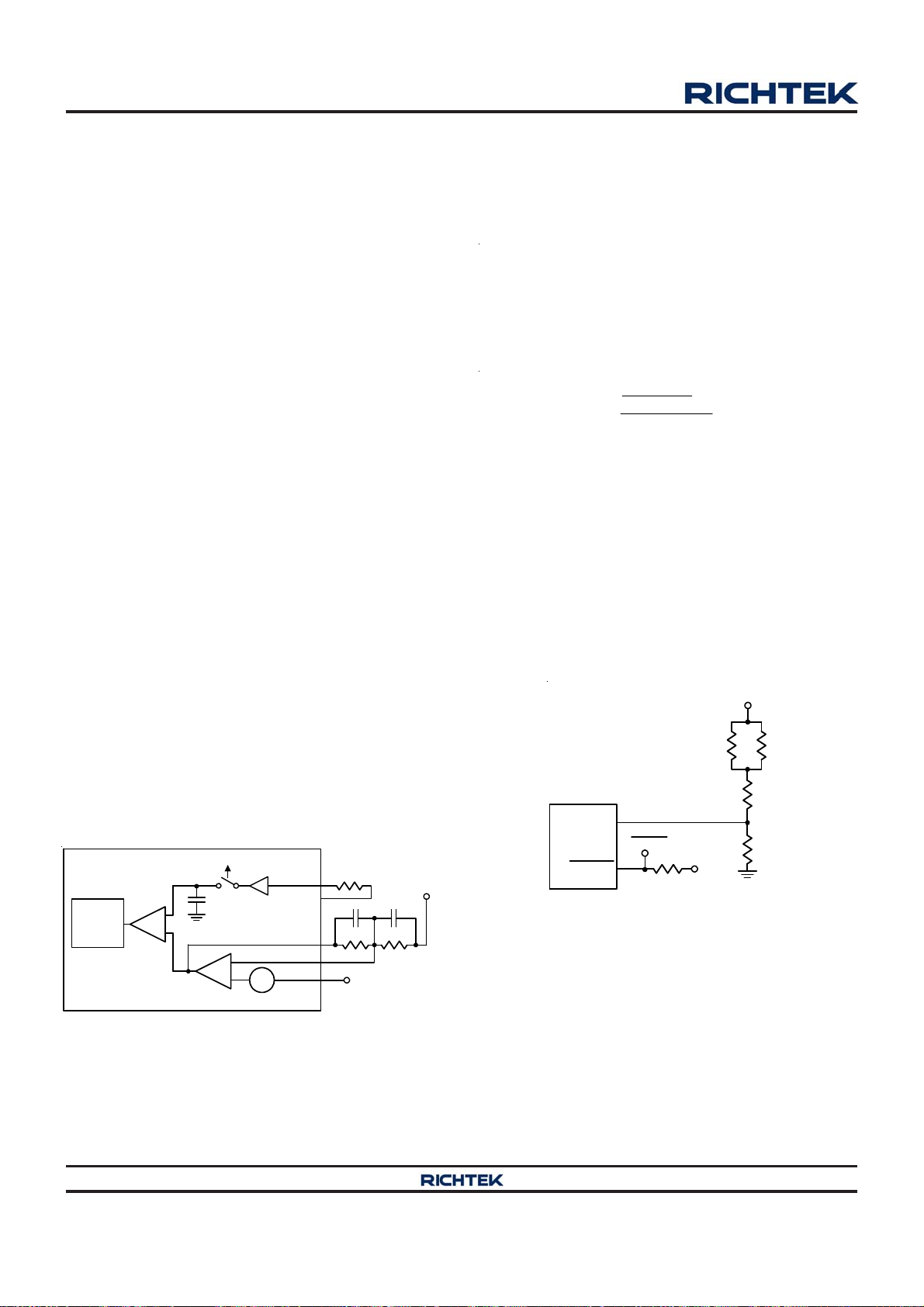
RT8885A
When the CORE VR receives SetPS command of PS2
operation mode, the CORE VR operates as a single phase
DCM controller, and only channel 1 is active with diode
emulation operation. The CORE VR will disable phase 2
and phase 3 by disabling Internal PWM logic drivers at
UGATE2 , LGATE2 and PWM3 pins (UGATE2 = 0V ,
LGATE2 = 0V , PWM = high impedance state). Therefore,
the external driver which support tri-state shutdown is
required for compatibility with PS2 operation state.
If the CORE VR receives dynamic VID change command
(SetVID), the CORE VR will automatically enter PS0
operation mode and all phases will be activated. After
V
OUT_CORE
reaches target voltage, the CORE VR will stay
at PS0 state. VR will ignore any former SetPS command
that CPU issues and asks CORE VR to be forced into
PS1 or PS2 operation states during dynamic VID process.
Dynamic VID Enhancement
During a dynamic VID transition, the charging (dynamic
VID up) or discharging (dynamic VID down) current causes
unwanted load-line effect which degrades the setting time
performance. In order to improve dynamic VID transition
performance, the RT8885A provides internalTM DVID
compensation function, as shown in Figure 16.
A switch (called DVID switch) turns on to observe sensed
current when the controller is normal operation. During a
dynamic VID transition, the switch turns off to hold sensed
current to compensate the charging or discharging current
effect. Therefore, the output voltage can be adjusted to
the target value more quickly.
CCRCOT
PWM
Logic
CMP
+
V
CS
DVID Event
-
EA
+
1/3
COMP
+
-
RGND
V
DAC
IMON
VREF
FB
R
IMON
C2 C1
R2
V
SS_SENSE
V
CC_SENSE
R1
Figure 16. InternalTM DVID Compensation Function
Ramp Amplitude Adjust
When the CORE VR enters PS2 operation mode, the
internal ramp of CORE VR will be modified for the reason
of stability. In case of smooth transition into PS2, the
CCM ramp amplitude should be designed properly. The
RT8885A provides RSET pin for platform users to set the
ramp amplitude of the CORE VR in CCM. The criterion is
to set the ramp amplitude proportional to the on-time. The
equation will be :
7
21.6 10 t V V
1 16 Ramp Factor 2.95%
()
ON IN DAC
[( ) ]
(56)
where 21.6 x 10⁻⁷ is an internal coefficient of analog circuit.
According to Equation 56 and Table 5, the ramp factor
equation can be simplified to :
R
TON
2.95%
4
1
(57)
Ramp Factor = 16
8.85 10
Thermal Monitoring and Temperature Reporting
The CORE VR provides thermal monitoring function via
sensing TSEN pin voltage. Through the voltage divider
resistors, R1, R
, R2, and R3, the voltage of TSEN will
NTC
be proportional to VR temperature as shown in Figure 17.
When VR temperature rises, TSEN voltage also rises.
The ADC circuit of the CORE VR monitors the voltage
variation at the TSEN pin from 1.4875V to 1.8725V with
55mV resolution. This voltage is then decoded into digital
format and stored into Temperature_Zone register.
VCC
TSEN
VRHOT
V
VRHOT
R1 R
VTT
R
TT
NTC
R2
R3
Figure 17. CORE VR : Thermal Monitoring Circuit
To meet Intel's VR12/IMVP7 specification, platform users
have to set the TSEN voltage to meet the temperature
variation of VR from 75% to 100% VR max temperature.
For example, if the VR max temperature is 100°C, platform
users have to set the TSEN voltage to be 1.5425V when
VR temperature reaches 82°C and 1.8725V when VR
temperature reaches 100°C. Detailed voltage setting
versus temperature variation is shown in Table 8. The
thermometer code is implemented in Temperature_Zone
register.
Copyright 2014 Richtek Technology Corporation. All rights reserved. is a registered trademark of Richtek Technology Corporation.
48
©
DS8885A-01 January 2014www.richtek.com
Page 49
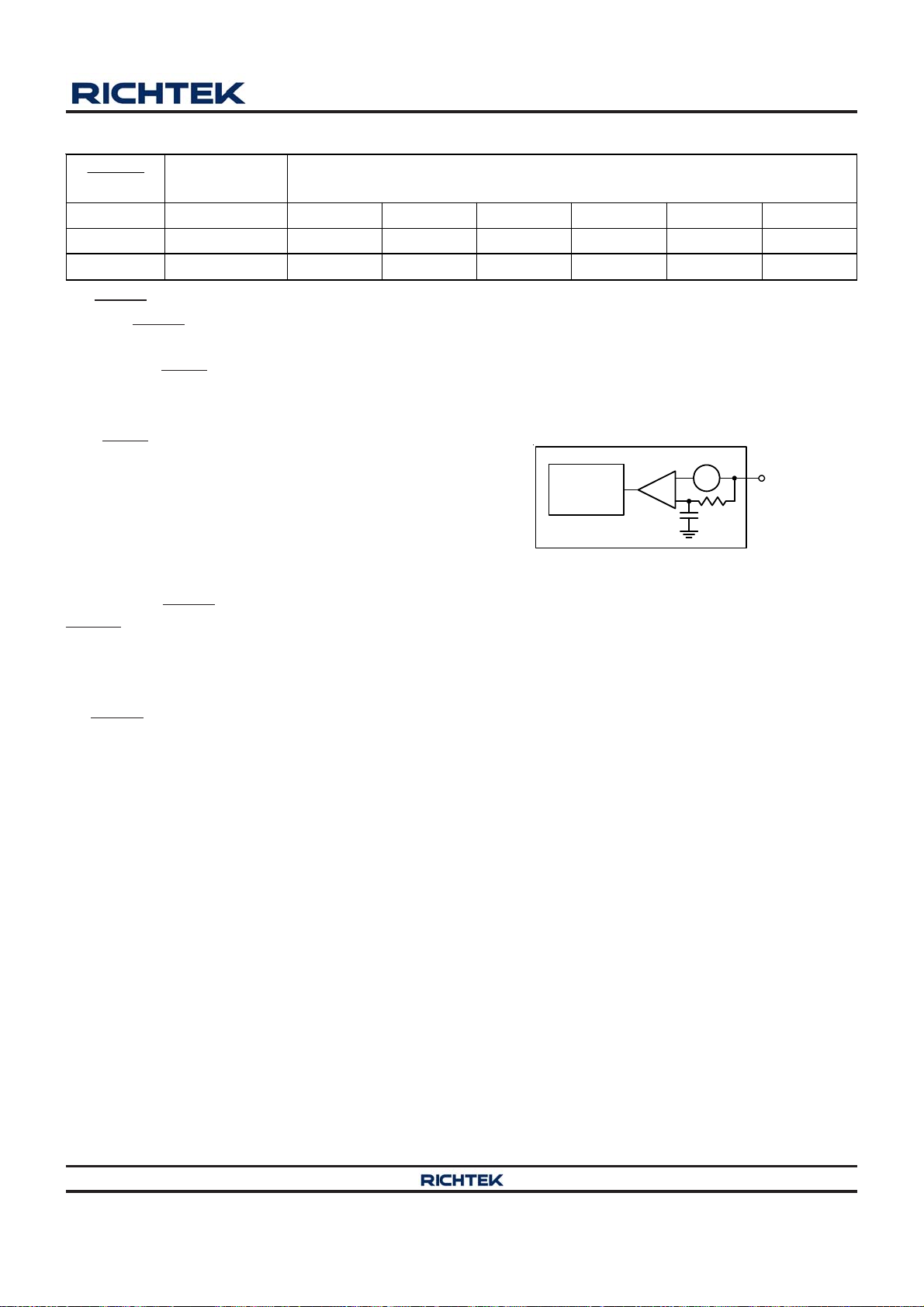
Table 8. Temperature_Zone Register
RT8885A
VRHOT
SVID Thermal
Alert
Comparator Trip Points Temperatures Scaled to maximum = 100%
Vo ltage Represents Assert bit Minimum Level
b7 b6 b5 b4 b3 b2 b1 b0
100% 97% 94% 91% 88% 85% 82% 75%
1.8725V 1.8175V 1.7625V 1.7075V 1.6525V 1.5975V 1.5425V 1.4875V
The VRHOT pin is an open-drain structure that sends out
active low VRHOT signal. When b6 of Temperature_Zone
register asserts to 1 (when TSEN voltage rises above
1.8175V), the ALERT signal will be asserted to low, which
is so-called SVID thermal alert. In the mean time, the
CORE VR will assert bit 1 data to 1 in Status_1 register.
The ALERT assertion will be de-asserted when b5 of
Temperature_Zone register is de-asserted from 1 to 0
(which means TSEN voltage falls under 1.7625V), and bit
times will be overridden by the quick response pulse.
Moreover, the quick response trigger threshold level,
QR_TH, is set by VREF/QRTH pin, and the quick response
pulse width, QR_TON, is set by SET1 pin. The detailed
pins setting refers to the VREF/QRTH and SET1 pin
setting section.
QR_TH
+
QR Pulse
Generation
Circuit
CMP
-
+
-
VSEN
1 of Status_1 register will also be cleared to 0. The bit 1
assertion of Status_1 is not latched and cannot be cleared
by GetReg command. When b7 of Temperature_Zone
register asserts to 1 (when TSEN voltage rises above
1.8725V), the VRHOT signal will be asserted to low. The
VRHOT assertion will be de-asserted when b6 of
Temperature_Zone register is de-asserted from 1 to 0
Figure 18. CORE VR : Quick Response Triggering
Circuit
Over Current Protection
The RT8885A provides summed total over current and per
phase over current protections.
(which means TSEN voltage falls under 1.8175V). It is
typically recommended to connect a pull-up resistor from
the VRHOT pin to a voltage source.
The controller determines summed total over current
protection SUM_OCP by comparing the I
IMON
with
SUM_OCP threshold whose setting refers to the OCSET
Quick Response
The RT8885A utilizes a quick response feature to support
heavy load current demand during instantaneous load
transient.
The controller monitors the abrupt VSEN pin voltage droop
to trigger QR pulse generation circuit, as shown in Figure
18. At steady state, the VSEN pin voltage droop cannot
trigger a quick response circuit. When this abrupt voltage
droop is lower than the QR trigger threshold level, the QR
circuit will be triggered. When quick response is triggered,
the quick response circuit will generate a quick response
pulse. The internal quick response pulse generation circuit
is similar to the on-time generation circuit. After generating
a quick response pulse, the pulse is then applied to the
on-time generation circuit, and all the active phases' on-
pin setting section. It declares SUM_OCP when I
above the SUM_OCP threshold for 40μs. When I
IMON
IMON
above the SUM_OCP threshold for 40μs, it declares
SUM_OCP. Therefore, latched SUM_OCP forces PWM
into high impedance, which disables internal PWM logic
drivers. Moreover, the GFX VR will also enter soft shut
down sequence.
The controller monitors either phase I
SENxN
current to
determine per phase over current protection PH_OCP. If
either phase I
current is greater than PH_OCP
SENxN
threshold for 100ns, the controller will declare fault and
PH_OCP latches off. Therefore, latched SUM_OCP forces
PWM into high impedance, which disables internal PWM
logic drivers. Moreover, the GFX VR will also enter soft
shut down sequence.
is
is
Copyright 2014 Richtek Technology Corporation. All rights reserved. is a registered trademark of Richtek Technology Corporation.
DS8885A-01 January 2014 www.richtek.com
©
49
Page 50

RT8885A
Over Voltage Protection (OVP)
The over voltage protection circuit of the CORE VR
monitors the output voltage via the VSEN pin after EN.
The supported maximum operating VID of the VR (V
(MAX)
is stored in the VOUT_Max register. If pin offset function
is enabled, the OVP threshold will be VMAX value plus
450mV. If not the OVP threshold will be VMAX value plus
150mV. Once V
OUT_CORE
exceeds OVP threshold, OVP
is triggered and latched. The CORE VR will try to turn on
low side MOSFETs and turn off high side MOSFETs of all
active phases of the CORE VR to protect the CPU. When
OVP is triggered by the CORE VR, the GFX VR will also
enter soft shut down sequence. A 1μs delay is used in
OVP detection circuit to prevent false trigger. OVP
detection circuit will have a 1μs trigger delay which can
prevent false trigger caused by any glitches. And only
VCC re-power or POR reset can release OVP latch.
Negative Voltage Protection (NVP)
During OVP latch state, the CORE VR also monitors the
VSEN pin for negative voltage protection. Since the OVP
latch continuously turns on all low side MOSFETs of the
CORE VR, the CORE VR may suffer negative output
voltage which is mainly caused by negative inductor
current. As a consequence, when the VSEN voltage drops
below −50mV after triggering OVP, the CORE VR will
trigger NVP to turn off all low side MOSFETs of the CORE
VR while the high side MOSFETs still remains off. After
triggering NVP, if the output voltage rises above 0V, the
NVP latch will be released and turn on all low side
MOSFETs due to OVP is still asserted. A 1μs trigger delay
is used in NVP detection circuit to prevent false trigger.
Under Voltage Protection (UVP)
The CORE VR implements under voltage protection of
V
OUT_CORE
. If pin offset function is enabled, the UVP
threshold will be VID minus 500mV. If not the OVP
threshold will be VID minus 400mV. Once V
OUT_CORE
is
less than the UVP threshold, the CORE VR will trigger
UVP latch. The UVP latch will turn off both high side and
low side MOSFETs. When UVP is triggered by the CORE
VR, the GFX VR will also enter soft shut down sequence.
A 3μs trigger delay is used in UVP detection circuit to
prevent false trigger. And only VCC re-power or POR reset
can release UVP latch.
Under Voltage Lock Out (UVLO)
During normal operation, if the voltage at the VCC pin
drops below POR threshold, the CORE VR will trigger
UVLO. The UVLO protection forces all high side MOSFETs
)
and low side MOSFETs off by shutting down internal PWM
logic drivers. A 3μs trigger delay is used in UVLO detection
circuit to prevent false trigger.
GFX VR
Active Phase Determination : Before EN
The number of active phases is determined by the internal
circuitry that monitors the ISENAxN voltages during start-
up. Normally, the GFX VR operates as a 2-phase PWM
controller. Setting ISENA2N to VCC before power-on can
program a 1-phase operation, and pulling ISENA1N, and
setting ISENA2N to VCC before power-on can disable GFX
VR operation. Before EN, GFX VR detects whether the
voltages of ISENA1N and ISENA2N are higher than “VCC
− 0.5V” respectively to decide how many phases should
be active. Phase selection is only active during EN. When
EN = high, the number of active phases is determined and
latched. The unused ISENAxP pins are recommended to
be connected to VCC and unused PWM pins can be left
floating.
Loop Control
The GFX VR adopts Richtek’s proprietary G-NAVP
topology. G-NAVPTM is based on the finite gain peak current
mode with CCRCOT (Constant Current Ripple Constant
On-Time) topology. The output voltage, V
decrease with increasing output load current. The control
loop consists of PWM modulators with power stages,
current sense amplifiers and an error amplifier as shown
in Figure 19.
Similar to the peak current mode control with finite
compensator gain, the HS_FET on-time is determined by
CCRCOT on-time generator. When load current increases,
VCS increases, the steady state COMPA voltage also
increases and induces V
OUT_GFX
to decrease, thus achieving
AVP. A near-DC offset canceling is added to the output of
EA to eliminate the inherent output offset of finite gain
peak current mode controller.
OUT_GFX
TM
will
Copyright 2014 Richtek Technology Corporation. All rights reserved. is a registered trademark of Richtek Technology Corporation.
50
©
DS8885A-01 January 2014www.richtek.com
Page 51
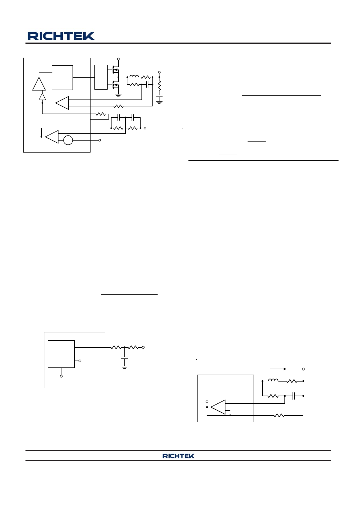
V
IN
CMP
CCRCOT
+
-
V
CS
1/3
COMP2
-
EA
+
PWM
Logic
GM
V
+
-
+
DAC
PWMAx
ISENAxP
ISENAxN
IMONA
VREF
COMPA
FBA
RGNDA
-
Driver
R
IMONA
HS_FET
LS_FET
R
CSx
R2
V
SSAXG_SENSE
R
C2 C1
R1
L
X
R
SENSE
C
X
V
V
OUT_GFX
R
C
C
CCAXG_SENSE
Figure 19. GFX VR : Simplified Schematic for Droop and
Remote Sense in CCM
TONA Setting
High frequency operation optimizes the application for the
smaller component size, trading off efficiency due to higher
switching losses. This may be acceptable in ultra portable
devices where the load currents are lower and the
controller is powered from a lower voltage supply. Low
frequency operation offers the best overall efficiency at
the expense of component size and board space. Figure
20 shows the On-Time setting Circuit. Connect a resistor
(R
) between V
TONA
and TONSETA to set the on-
IN_GFX
time of UGATE :
12
t (0.5VV 1.2V)
ON DAC
24.4 10 R
VV
IN DAC
where tON is the UGATE turn on period, V
input voltage of the GFX VR, and V
is the DAC voltage.
DAC
TONA
(58)
is the
IN_GFX
RT8885A
implements a pseudo constant frequency technology to
avoid this disadvantage of CCRCOT topology. When V
is larger than 1.2V, the on-time equation will be modified
to :
12
t (V 1.2V)
ON DAC
20.33 10 R V
VV
TONA DAC
IN DAC
On-time translates only roughly to switching frequencies.
For better efficiency of the given load range, the maximum
switching frequency is suggested to be :
f
SW(MAX)
where f
V
mode or HFM, V
(t 60ns) R 50ns
ON ON _ LS FET(MAX)
IccTDC
VDCRRNR
DAC _ PS0 ON _ LS FET(MAX) DROOP
VRR
IN(MAX) ON _ LS FET(MAX) ON_ HS FET(MAX )
DAC_PS0
N
ITDC
CC
N
is the maximum switching frequency,
S(MAX)
is the test VID of application at PS0 for turbo
IN(MAX)
IccTDC
is the maximum application input
1
N
voltage, IccTDC is the thermal design current of application,
N is the phase number, R
equivalent high side FET R
ON_HS-FET(MAX)
DS(ON)
maximum equivalent low side FET R
inductor DCR, and R
is the load line setting.
DROOP
is the maximum
, R
ON_LS-FET(MAX)
DS(ON)
, DCR is the
Current Sense Setting
The current sense topology of the GFX VR is continuous
inductor current sensing. Therefore, the controller has less
noise sensitive. Low offset amplifiers are used for current
balance, loop control and over current detection. The
ISENAxP and ISENAxN pins denote the positive and
negative input of the current sense amplifier of each phase.
DAC
(59)
(60)
is the
Users can either use a current-sense resistor or the
CCRCOT
On-Time
Computer
On-Time
TONSETA
V
DAC
R
Figure 20. GFX VR : On-Time Setting with RC Filter
When V
is larger than 1.2V, the equivalent switching
DAC
TONA
R1
C1
V
IN
inductor's DCR for current sensing. Using the inductor’s
DCR allows higher efficiency as shown in Figure 21.
V
DCR
C
OUT_GFX
X
I
SENAxN
+
-
ISENAxP
ISENAxN
I
L
L
R
X
R
CSx
frequency may be over 500kHz, and this too fast switching
frequency is unacceptable. Therefore, the GFX VR
Copyright 2014 Richtek Technology Corporation. All rights reserved. is a registered trademark of Richtek Technology Corporation.
DS8885A-01 January 2014 www.richtek.com
©
Figure 21. GFX VR : Lossless Inductor Sensing
51
Page 52

RT8885A
In order to optimize transient performance, RX and CX must
be set according to the equation below :
L
DCR
RC
X
X
(61)
Then the proportion between the phase current IL and the
sensed current I
DCR
II
SENAxN L
where R
R
is only an exact 680Ω sense resistor. The
CSx
resistance accuracy of R
can be described as below :
SENAxN
CSx
is recommended to be 1% or
CSx
(62)
higher.
In addition to considering the inductance tolerance, the
resistor RX has to be tuned on board by examining the
transient voltage. If the output voltage transient has an
initial dip below the minimum load line requirement and
the recovery is too fast causing a ring back. Vice versa,
with a resistance too large the output voltage transient
has only a small initial dip with a slow recovery.
Using current sense resistor in series with the inductor
can have better accuracy, but the efficiency is a trade-off.
Considering the equivalent inductance (L
) of the current
ESL
sense resistor, an RC filter is recommended. The RC filter
calculation method is similar to the above mentioned
inductor DCR sensing method.
Current Monitoring and Current Reporting
The RT8885A provides the current monitor function for GFX
VR. IMONA pin reports GFX VR inductor current.
The IMONA pin outputs a high-speed analog current source
that is 1 time of the summed current. Thus I
IMONA
can be
described as below :
II
IMONA SENAxN
(63)
The RT8885A monitors the IMONA pin voltage and
considers that GFX VR has reached ICCMAXA when
IMONA pin voltage is 2.392V.
As Figure 19 show, a resistor R
the IMONA pin and VREF pin. Through the R
is connected between
IMONA
IMONA
to
convert the IMONA pin current to voltage. The voltage of
IMONA pin is expressed in Equation 64 :
VIR0.6
IMONA IMONA IMONA
(64)
Rewriting Equations 62 and 63 gives Equation 65 :
DCR
II
IMONA LOAD
R
CSx
(65)
Substitution of Equation 65 into Equation 64 gives
Equation 66 :
DCR
VIR0.6
IMONA LOAD IMONA
R
CSx
(66)
Rewriting Equation 66 and application of full load condition
gives Equation 67 :
R(V 0.6)
CSx IMONA
R
IMONA
DCR I
For example, given R
= 2.392V at I
LOAD(MAX)
LOAD
= 680Ω, DCR = 0.82mΩ, V
CSx
= 53A, Equation 65 gives R
(67)
IMONA
IMONA
=
28kΩ.
In addition, Richtek provides a Microsoft Excel-based
spreadsheet to help design the IMONA resistor network
with temperature compensation for GFX VR.
Droop Setting
It's very easy to achieve Active Voltage Positioning (AVP)
by properly setting the error amplifier gain due to the native
droop characteristics. This target is to have
VVI R
OUT DAC LOAD DROOP
Then solving the switching condition V
COMP2
(68)
= VCS in
Figure 19 yields the desired error amplifier gain as
R2
A
V
R1 R
where R
G
I
DROOP
is the equivalent load line resistance as
DROOP
(69)
well as the desired static output impedance.
The summed current sense gain GI as
R
SENSE
GR
IIMONA
R3
CSx
where R
is the current-sense resistor. If no external
SENSE
sense resistor present, it is the DCR of the inductor. R
is the sense resistor. R
1
is the equivalent resistance
IMONA
(70)
CSx
of temperature dependent resistor.
Droop Disable
Refer to the TSENA pin setting section, disabling the GFX
VR droop can be set by platform users through the TSENA
pin.
Loop Compensation
Optimized compensation of the GFX VR allows for best
possible load step response of the regulator's output. A
type-I compensator with one pole and one zero is adequate
for proper compensation. Figure 19 shows the
Copyright 2014 Richtek Technology Corporation. All rights reserved. is a registered trademark of Richtek Technology Corporation.
52
©
DS8885A-01 January 2014www.richtek.com
Page 53

RT8885A
compensation circuit. Prior design procedure shows how
to select the resistive feedback components for the error
amplifier gain. Next, C1 and C2 must be calculated for
compensation. The target is to achieve constant resistive
output impedance over the widest possible frequency
range.
The pole frequency of the compensator must be set to
compensate the output capacitor ESR zero :
f
p
1
2CR
C
(71)
where C is the capacitance of output capacitor, and RC is
the ESR of output capacitor. C2 can be calculated as
follows :
C2
C
R2
(72)
CR
The zero of compensator has to be placed at half of the
switching frequency to filter the switching related noise.
Such that,
C1
1
R1 f
SW
(73)
Differential Remote Sense Setting
The GFX VR includes differential, remote-sense inputs to
eliminate the effects of voltage drops along the PC board
traces, CPU internal power routes and socket contacts.
Figure 22 shows the GFX VR differential remote voltage
sense connection. The CPU contains on-die sense pins,
V
CCAXG_SENSE
V
SSAXG_SENSE
and V
SSAXG_SENSE
. Connect FBA to V
. Connect RGNDA to
CCAXG_SENSE
with a resistor
to build the negative input path of the error amplifier. The
V
and the precision voltage reference are referred to
DAC
RGNDA for accurate remote sensing.
CPU V
CCAXG_SENSE
Compensation
To
RGNDA
R3 R1
R4 R2
CPU V
SSAXG_SENSE
C1C2
V
OUT_GFX
GND
Figure 22. GFX VR : Differential Remote Voltage Sense
Connection
Current Balance
The GFX VR implements internal current balance
mechanism in the current loop. The GFX VR senses and
compares per-phase current signal with average current.
If the sensed current of any particular phase is larger than
average current, the on-time of this phase will be adjusted
to be shorter.
No Load Offset (SVID & Platform)
The GFX VR features no load offset function which provides
the possibility of wide range positive offset of output voltage.
The no-load offset function can be implemented through
the SVID interface or RSETA/OFSA pin. Users can disable
pin offset function by simply connecting RSETA/OFSA
pin to GND. The RT8885A will latch the RSETA/OFSA
status after EN goes high.
If pin offset function is enabled, then the output voltage is
VVIR
OUT _ GFX DAC LOAD DROOP
V V
SVID OFS PIN OFS
(74)
If not the output voltage is
VVIRV
OUT _ GFX DAC LOAD DROOP SVID OFS
(75)
The pin offset voltage is set by the divider voltage on
RSETA/OFSA pin. The linear range of offset pin voltage is
from 1V to 1.4V. The pin offset voltage can be calculated
as below :
VV1.2V
PIN OFS OFS
(76)
For example, supplying 1.3V at RSETA/OFSA pin will
achieve 100mV offset at the output.
Operation Mode Transition
The RT8885A supports operation mode transition function
at the GFX VR for the SetPS command of Intel's VR12/
IMVP7 CPU. The default operation mode of the GFX VR
is PS0, which is full phase CCM operation. Other operation
modes includes PS1 (single phase CCM operation) and
PS2 (single phase DEM operation).
After receiving SetPS command, the GFX VR will
immediately change to the new operation state. When
the GFX VR receives SetPS command of PS1 operation
mode, the GFX VR operates as a single phase CCM
controller, and only channel 1 is active. The GFX VR will
disable PWMA2 pins. Therefore, the external driver which
supports tri-state shutdown is required for compatibility
with PS1 operation mode.
When the GFX VR receives SetPS command of PS2
operation mode, the GFX VR operates as a single phase
Copyright 2014 Richtek Technology Corporation. All rights reserved. is a registered trademark of Richtek Technology Corporation.
DS8885A-01 January 2014 www.richtek.com
©
53
Page 54
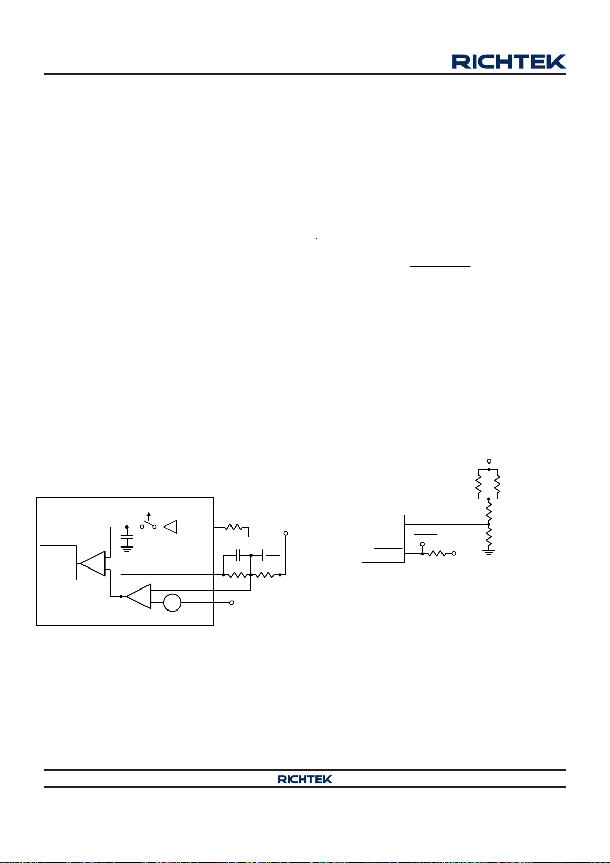
RT8885A
DCM controller, and only channel 1 is active with diode
emulation operation. The GFX VR will disable PWMA2
pins. Therefore, the external driver which supports tri-state
shutdown is required for compatibility with PS2 operation
state.
If the GFX VR receives dynamic VID change command
(SetVID), the GFX VR will automatically enter PS0
operation mode and all phases will be activated. After
V
OUT_GFX
reaches target voltage, the GFX VR will stay at
PS0 state. VR will ignore any former SetPS command
that CPU issues and asks GFX VR to be forced into PS1
or PS2 operation states during dynamic VID process.
Dynamic VID Enhancement
During a dynamic VID transition, the charging (dynamic
VID up) or discharging (dynamic VID down) current causes
unwanted load-line effect which degrades the setting time
performance. In order to improve dynamic VID transition
performance, the RT8885A provides internalTM DVID
compensation function, as shown in Figure 23.
A switch (called DVID switch) turns on to observe sensed
current when the controller is normal operation. During a
dynamic VID transition, the switch turns off to hold sensed
current to compensate the charging or discharging current
effect. Therefore, the output voltage can be adjusted to
the target value more quickly.
provides RSETA pin for platform users to set the ramp
amplitude of the GFX VR in CCM. The criterion is to set
the ramp amplitude proportional to the on-time. The
equation will be :
7
21.6 10 t V V
1 16 Ramp Factor 2.95%
()
ON IN DAC
[( ) ]
(77)
where 21.6 x 10⁻⁷ is an internal coefficient of analog circuit.
According to Equation 77 and Table 6, the Ramp Factor
equation can be simplified to :
TONA
2.95%
4
1
(78)
Ramp Factor = 16
8.85 10
R
Thermal Monitoring and Temperature Reporting
The GFX VR provides thermal monitoring function via
sensing TSENA pin voltage. Through the voltage divider
resistors, R1, R
, R2, and R3, the voltage of TSENA
NTC
will be proportional to VR temperature as shown in Figure
24. When VR temperature rises, TSENA voltage also rises.
The ADC circuit of the GFX VR monitors the voltage
variation at the TSENA pin from 1.4875V to 1.8725V with
55mV resolution. This voltage is then decoded into digital
format and stored into Temperature_Zone register.
VCC
R1 R
NTC
CCRCOT
PWM
Logic
CMP
+
V
CS
DVID Event
-
EA
+
V
+
1/3
DAC
IMONA
COMPA
-
RGNDA
VREF
FBA
R
IMONA
C2 C1
R2
V
SSAXG_SENSE
V
CCAXG_SENSE
R1
TSENA
V
VRHOT
VRHOT
VTT
R
TT
Figure 24. GFX VR : Thermal Monitoring Circuit
To meet Intel's VR12/IMVP7 specification, platform users
have to set the TSENA voltage to meet the temperature
R2
R3
variation of VR from 75% to 100% VR max temperature.
Figure 23. InternalTM DVID Compensation Function
For example, if the VR max temperature is 100°C, platform
users have to set the TSENA voltage to be 1.5425V when
Ramp Amplitude Adjust
When the GFX VR enters PS2 operation mode, the
internal ramp of GFX VR will be modified for the reason of
stability. In case of smooth transition into PS2, the CCM
ramp amplitude should be designed properly. The RT8885A
Copyright 2014 Richtek Technology Corporation. All rights reserved. is a registered trademark of Richtek Technology Corporation.
54
©
VR temperature reaches 82°C and 1.8725V when VR
temperature reaches 100°C. Detailed voltage setting
versus temperature variation is shown in Table 9. The
thermometer code is implemented in Temperature_Zone
register.
DS8885A-01 January 2014www.richtek.com
Page 55
Table 9. Temperature_Zone Register
RT8885A
VRHOT
SVID Thermal
Alert
Comparator Trip Points Temperatures Scaled to maximum = 100%
Vo ltage Represents Assert bit Minimum Level
b7 b6 b5 b4 b3 b2 b1 b0
100% 97% 94% 91% 88% 85% 82% 75%
1.8725V 1.8175V 1.7625V 1.7075V 1.6525V 1.5975V 1.5425V 1.4875V
The VRHOT pin is an open-drain structure that sends out
active low VRHOT signal. When b6 of Temperature_Zone
register asserts to 1 (when TSENA voltage rises above
1.8175V), the ALERT signal will be asserted to low, which
is so-called SVID thermal alert. In the mean time, the
GFX VR will assert bit 1 data to 1 in Status_1 register.
The ALERT assertion will be de-asserted when b5 of
threshold level, QR_TH, is set by VREF/QRTH pin, and
the quick response pulse width, QR_TON, is set by SET2
pin. The detailed pins setting refers to the VREF/QRTH
and SET2 pin setting section.
QR_TH
+
QR Pulse
Generation
Circuit
CMP
-
+
-
VSENA
Temperature_Zone register is de-asserted from 1 to 0
(which means TSENA voltage falls under 1.7625V), and
bit 1 of Status_1 register will also be cleared to 0. The bit
1 assertion of Status_1 is not latched and cannot be
Figure 25. GFX VR : Quick Response Triggering Circuit
Over Current Protection
cleared by GetReg command. When b7 of
Temperature_Zone register asserts to 1 (when TSENA
voltage rises above 1.8725V), the VRHOT signal will be
asserted to low. The VRHOT assertion will be de-asserted
when b6 of Temperature_Zone register is de-asserted from
1 to 0 (which means TSENA voltage falls under 1.8175V).
It is typically recommended to connect a pull-up resistor
from the VRHOT pin to a voltage source.
The RT8885A provides summed total over current and per
phase over current protections.
The controller determines summed total over current
protection SUM_OCP by comparing the I
IMONA
with
SUM_OCP threshold whose setting refers to the OCSET
pin setting section. It declares SUM_OCP when I
above the SUM_OCP threshold for 40μs. When I
IMONA
IMONA
above the SUM_OCP threshold for 40μs, it declares
Quick Response
The RT8885A utilizes a quick response feature to support
heavy load current demand during instantaneous load
transient.
SUM_OCP. Therefore, latched SUM_OCP forces PWM
into high impedance, which disables internal PWM logic
drivers. Moreover, the GFX VR will also enter soft shut
down sequence.
is
is
The controller monitors the abrupt VSENA pin voltage
droop to trigger QR pulse generation circuit, as shown in
Figure 25. At steady state, the VSENA pin voltage droop
cannot trigger a quick response circuit. When this abrupt
voltage droop is lower than the QR trigger threshold level,
the QR circuit will be triggered. When quick response is
triggered, the quick response circuit will generate a quick
response pulse. The internal quick response pulse
The controller monitors either phase I
SENAxN
current to
determine per phase over current protection PH_OCP. If
either phase I
current is greater than PH_OCP
SENAxN
threshold for 100ns, the controller will declare fault and
PH_OCP latches off. Therefore, latched SUM_OCP forces
PWM into high impedance, which disables internal PWM
logic drivers. Moreover, the CORE VR will also enter soft
shut down sequence.
generation circuit is similar to the on-time generation
circuit. After generating a quick response pulse, the pulse
is then applied to the on-time generation circuit, and all
the active phases' on-times will be overridden by the quick
response pulse. Moreover, the quick response trigger
Copyright 2014 Richtek Technology Corporation. All rights reserved. is a registered trademark of Richtek Technology Corporation.
DS8885A-01 January 2014 www.richtek.com
©
Over Voltage Protection (OVP)
The over voltage protection circuit of the GFX VR monitors
the output voltage via the VSENA pin after EN. The
supported maximum operating VID of the VR (V
(MAX)
) is
55
Page 56

RT8885A
stored in the VOUT_Max register. If pin offset function is
enabled, the OVP threshold will be VMAX value plus
450mV. If not the OVP threshold will be VMAX value plus
150mV. Once V
OUT_GFX
exceeds OVP threshold, OVP is
triggered and latched. The GFX VR will try to turn on low
side MOSFETs and turn off high side MOSFETs of all
active phases of the GFX VR to protect the CPU. When
OVP is triggered by the GFX VR, the CORE VR will also
enter soft shut down sequence. A 1μs delay is used in
OVP detection circuit to prevent false trigger. OVP
detection circuit will have a 1μs trigger delay which can
prevent false trigger caused by any glitches. And only
VCC re-power or POR reset can release OVP latch.
Negative Voltage Protection (NVP)
During OVP latch state, the GFX VR also monitors the
VSENA pin for negative voltage protection. Since the OVP
latch continuously turns on all low side MOSFETs of the
GFX VR, the GFX VR may suffer negative output voltage
which is mainly caused by negative inductor current. As
a consequence, when the VSENA voltage drops below −
50mV after triggering OVP, the GFX VR will trigger NVP
to turn off all low side MOSFETs of the GFX VR while the
high side MOSFETs still remains off. After triggering NVP,
if the output voltage rises above 0V, the NVP latch will be
released and turn on all low side MOSFETs due to OVP
is still asserted. A 1μs trigger delay is used in NVP
detection circuit to prevent false trigger.
Under Voltage Protection (UVP)
The GFX VR implements under voltage protection of
V
OUT_GFX
. If pin offset function is enabled, the UVP
threshold will be VID minus 500mV. If not the OVP
threshold will be VID minus 400mV. Once V
OUT_GFX
is
less than the UVP threshold, the GFX VR trigger UVP
latch. The UVP latch will turns off both high side and low
side MOSFETs. When UVP is triggered by the GFX VR,
the CORE VR will also enter soft shut down sequence. A
3μs trigger delay is used in UVP detection circuit to
prevent false trigger. And only VCC re-power or POR reset
can release UVP latch.
Under Voltage Lock Out (UVLO)
During normal operation, if the voltage at the VCC pin
drops below POR threshold, the GFX VR will trigger UVLO.
The UVLO protection forces all high side MOSFETs and
low side MOSFETs off by shutting down internal PWM
logic drivers. A 3μs trigger delay is used in UVLO detection
circuit to prevent false trigger.
Inductor Selection
The switching frequency and ripple current determine the
inductor value as follows :
VV
L = T
MIN ON
IN OUT
I
Ripple(MAX)
(79)
where tON is the UGATE turn-on period.
Higher inductance yields less ripple current and hence
higher efficiency. The downside is a slower transient
response of the power stage to load transients. This might
increase the need for more output capacitors, thus driving
up the cost. Select a low loss inductor having the lowest
possible DC resistance that fits in the allotted dimensions.
The core must be large enough not to be saturated at the
peak inductor current.
Output Capacitor Selection
Output capacitors are used to obtain high bandwidth for
the output voltage beyond the bandwidth of the converter
itself. Usually, the CPU manufacturer recommends a
capacitor configuration. Two different kinds of output
capacitors are typically used : bulk capacitors closely
located next to the inductors, and ceramic output
capacitors in close proximity to the load. Latter ones are
for mid-frequency decoupling with especially small ESR
and ESL values, while the bulk capacitors have to provide
stored energy enough to overcome the low frequency
bandwidth gap between the regulator and the CPU.
Thermal Considerations
For continuous operation, do not exceed absolute
maximum junction temperature. The maximum power
dissipation depends on the thermal resistance of the IC
package, PCB layout, rate of surrounding airflow, and
difference between junction and ambient temperature. The
maximum power dissipation can be calculated by the
following formula :
Copyright 2014 Richtek Technology Corporation. All rights reserved. is a registered trademark of Richtek Technology Corporation.
56
©
DS8885A-01 January 2014www.richtek.com
Page 57
RT8885A
P
where T
D(MAX)
= (T
J(MAX)
− TA) / θ
J(MAX)
JA
is the maximum junction temperature, TA is
the ambient temperature, and θJA is the junction to ambient
thermal resistance.
For recommended operating condition specifications of
the RT8885A, the maximum junction temperature is 125°C
and TA is the ambient temperature. The junction to ambient
thermal resistance, θJA, is layout dependent. For WQFN-
56L 7x7 package, the thermal resistance, θJA, is 31°C/W
on a standard JEDEC 51-7 four-layer thermal test board.
The maximum power dissipation at TA = 25°C can be
calculated by the following formula :
P
= (125°C − 25°C) / (31°C/W) = 3.226W for
D(MAX)
WQFN-56L 7x7 package
The maximum power dissipation depends on the operating
ambient temperature for fixed T
J (MAX)
and thermal
resistance, θJA. For RT8885A package, the derating curve
in Figure 26 allows the designer to see the effect of rising
ambient temperature on the maximum power dissipation.
3.5
3.0
2.5
Four-Layers PCB
Layout Considerations
Careful PC board layout is critical to achieve low switching
losses and clean, stable operation. The switching power
stage requires particular attention. If possible, mount all
of the power components on the top side of the board
with their ground terminals flushed against one another.
Follow these guidelines for optimum PC board layout :
Keep the high current paths short, especially at the
ground terminals.
Keep the power traces and load connections short. This
is essential for high efficiency.
When trade-offs in trace lengths must be made, it’s
preferable to let the inductor charging path be longer
than the discharging path.
Place the current sense component close to the
controller. ISENxP and ISENxN connections for current
limit and voltage positioning must be made using Kelvin
sense connections to guarantee current sense accuracy.
The PCB trace from the sense nodes should be
paralleled back to the controller.
Route high speed switching nodes away from sensitive
analog areas (COMP, FB, ISENxP, ISENxN, etc...)
2.0
1.5
1.0
0.5
Maximum Power Dissipation (W)1
0.0
0 25 50 75 100 125
Ambient Temperature (°C)
Figure 26. Derating Curve for RT8885A Package
Copyright 2014 Richtek Technology Corporation. All rights reserved. is a registered trademark of Richtek Technology Corporation.
DS8885A-01 January 2014 www.richtek.com
©
57
Page 58

RT8885A
Outline Dimension
1
2
DETAIL A
Pin #1 ID and Tie Bar Mark Options
Note : The configuration of the Pin #1 identifier is optional,
but must be located within the zone indicated.
Dimensions In Millimeters Dimensions In Inches
Symbol
Min Max Min Max
A 0.700 0.800 0.028 0.031
A1 0.000 0.050 0.000 0.002
A3 0.175 0.250 0.007 0.010
b 0.150 0.250 0.006 0.010
D 6.900 7.100 0.272 0.280
D2 5.150 5.250 0.203 0.207
E 6.900 7.100 0.272 0.280
E2 5.150 5.250 0.203 0.207
1
2
e 0.400 0.016
L 0.350 0.450
Copyright 2014 Richtek Technology Corporation. All rights reserved. is a registered trademark of Richtek Technology Corporation.
58
©
W-Type 56L QFN 7x7 Package
0.014 0.018
DS8885A-01 January 2014www.richtek.com
Page 59

RT8885A
Richtek Technology Corporation
14F, No. 8, Tai Yuen 1st Street, Chupei City
Hsinchu, Taiwan, R.O.C.
Tel: (8863)5526789
Richtek products are sold by description only. Richtek reserves the right to change the circuitry and/or specifications without notice at any time. Customers should
obtain the latest relevant information and data sheets before placing orders and should verify that such information is current and complete. Richtek cannot
assume responsibility for use of any circuitry other than circuitry entirely embodied in a Richtek product. Information furnished by Richtek is believed to be
accurate and reliable. However, no responsibility is assumed by Richtek or its subsidiaries for its use; nor for any infringements of patents or other rights of third
parties which may result from its use. No license is granted by implication or otherwise under any patent or patent rights of Richtek or its subsidiaries.
DS8885A-01 January 2014 www.richtek.com
59
 Loading...