

Preliminary
RT8805
Two Phase General Purpose PWM Controller
General Description
The RT8805 is the most compact dual-phase synchronous
buck controller in the industry specifically designed for
high power density applications. This part is capable of
delivering up to 60A output current due to its embedded
bootstrapped drivers that support 12V + 12V driving
capability.
The phase currents are sensed by innovative time sharing
R
current sensing technique for current balance and
DS(ON)
over current balance. Using one common GM amplifier to
sense two phase currents eliminates offset and
nonlinearity of the GM amplifier and yields good current
balance. Other features include adjustable operation
frequency from 50kHz to 1MHz, adjustable soft-start,
PGOOD, external compensation, enable/shutdown for
various application and performance consideration.
The RT8805 comes to a tiny footprint package of
VQFN-16L 3x3 package that is capable of dissipating up
to 1.47W heat.
Ordering Information
RT8805
Features
zz
12V Power Supply Voltage
z
zz
zz
z 2 Phase Power Conversion
zz
zz
z Embedded 12V Boot Strapped Driver
zz
zz
z Precise Core Voltage Regulation
zz
zz
z Low Side MOSFET R
zz
Current Sensing for
DS(ON)
Power Stage Current Balance
zz
z External Compensation
zz
zz
z Adjustable Soft-Start
zz
zz
z Adjustable Frequency and Typical at 300kHz Per
zz
Phase
zz
z Power Good Indication
zz
zz
z Adjustable Over Current Protection
zz
zz
z Small 16-Lead VQFN Package
zz
zz
z RoHS Compliant and 100% Lead (Pb)-Free
zz
Applications
z Middle-High End GPU Core Power
z High End Desktop PC Memory Core Power
z Low Output Voltage, High Power Density DC-DC
Converters
z Voltage Regulator Modules
Package Type
QV : VQFN-16L 3x3 (V-Type)
Operating Temperature Range
P : Pb Free with Commercial Standard
Note :
RichTek Pb-free products are :
`RoHS compliant and compatible with the current require-
ments of IPC/JEDEC J-STD-020.
`Suitable for use in SnPb or Pb-free soldering processes.
`100% matte tin (Sn) plating.
Marking Information
For marking information, contact our sales representative
directly or through a RichTek distributor located in your
area, otherwise visit our website for detail.
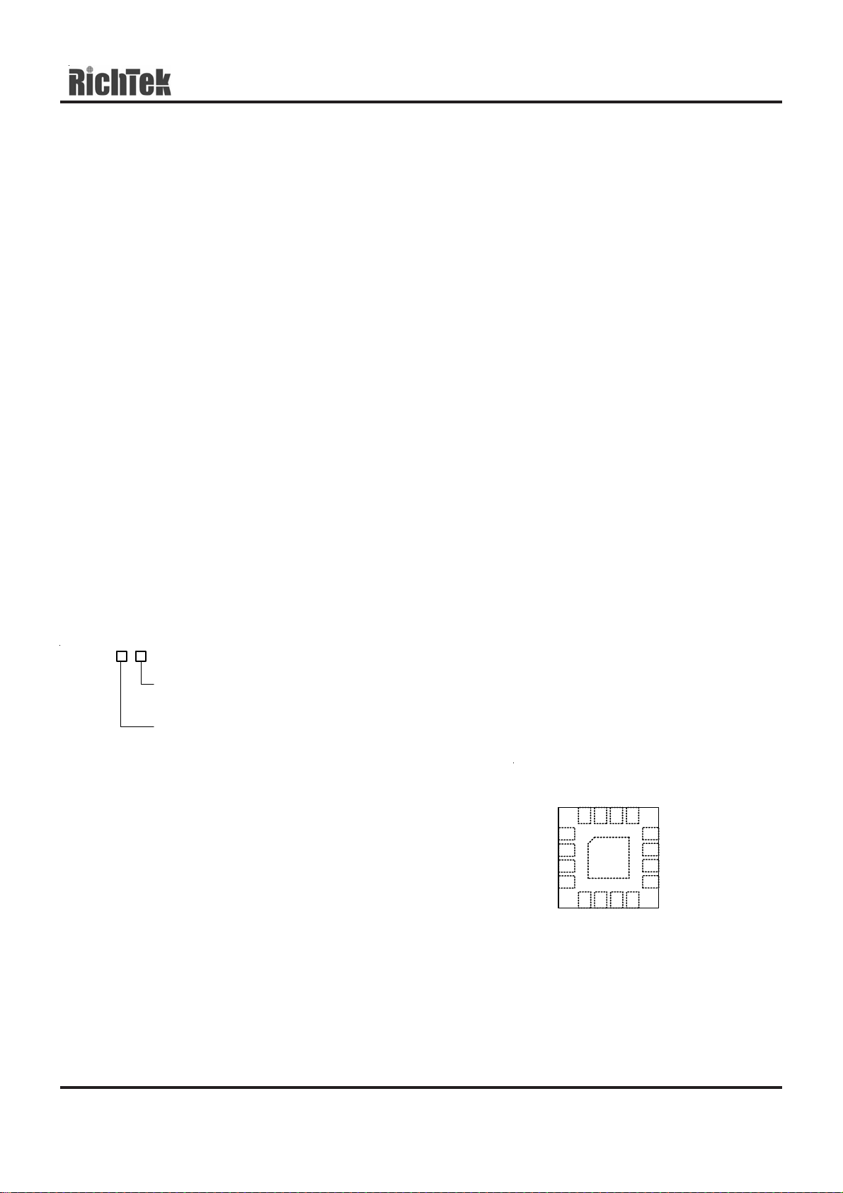
Pin Configurations
(TOP VIEW)
PHASE1
LGATE1
UGATE1
BOOT1
AGND
IMAX
1
2
GND
3
4
RT
SS
VQFN-16L 3x3
VCC
13141516
COMP
LGATE2
PHASE2
12
UGATE2
11
BOOT2
10
PGOOD
9
8765
FB
DS8805-01 November 2005 www.richtek.com
1
RT8805
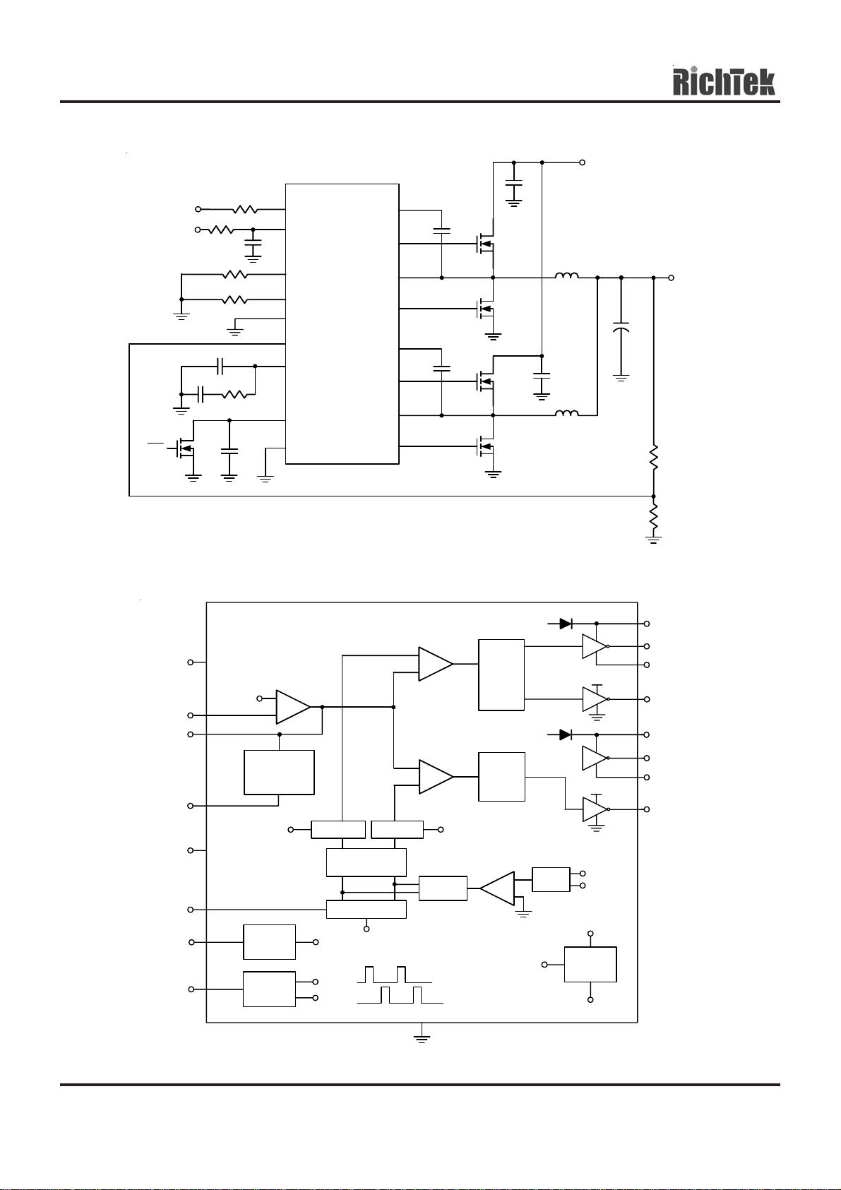
Typical Application Circuit
Preliminary
V
IN
R8
9
14
C9
5
4
3
8
7
6
C3
EN
3.3V
12V
CC
CC
C2
R9
R1
R2
C1
R3
Q5
Function Block Diagram
PGOOD
VCC
RT
IMAX
AGND
FB
COMP
SS
GND
RT8805
BOOT1
UGATE1
PHASE1
LGATE1
BOOT2
UGATE2
PHASE2
LGATE2
2
1
16
15
10
11
12
13
C4
C6
Q1
Q2
Q3
Q4
C5
C7
L1
L2
C8
R4
R5
V
OUT
PGOOD
FB
COMP
SS
AGND
IMAX
VCC
RT
0.8V
+
EA
-
External
Soft Star
Reg
Clock
V
DD
CLK1
CLK2
Current
Balance
OCP
OC
V
CC
PWMCP
+
PWMCP
+
-
RAMP2RAMP1
S/H
PWM1
Logic
V
CC
PWM2
Logic
CLK2CLK1
-
GM
MUX
+
PGOOD
V
CC
V
CC
PHASE2
PHASE1
To PWM Logic
Central
Logic
OC
BOOT1
UGATE1
PHASE1
LGATE1
BOOT2
UGATE2
PHASE2
LGATE2
GND
DS8805-01 November 2005www.richtek.com
2

Functional Pin Description
Preliminary
RT8805
UGA TE1 (Pin 1), UGA TE2 (Pin 11)
Upper Gate Drive. These pins drive the gates of the highside
MOSFETs.
BOOT1 (Pin 2), BOOT2 (Pin 10)
Bootstrap Power Pin. These pins power the high-side
MOSFET drivers. Connect These pins to the junctions of
the bootstrap capacitors.
AGND (Pin 3)
Chip Analog Ground.
IMAX (Pin 4)
Maximum Current Setting. This pin sets the current limiting
level. Connect this pin with resistor to ground to set the
current limit.
RT (Pin 5)
Timing Resistor. Connect a resistor from RT to AGND to
set the clock frequency.
PHASE1 (Pin 16), PHASE2 (Pin 12)
These pins are return nodes of the high-side driver.
Connect These pins to high-side MOSFET sources
together with the low-side MOSFET drains and the
inductors.
VCC (Pin 14)
The VCC pin is the external 12V power. Internal 5V power
(VDD) is regulated from this pin. This pin also powers the
low side MOSFETS drivers.
GND (Exposed Pad)
Exposed pad should be soldered to PCB board and
connected to GND.
SS (Pin 6)
Soft-Start Pin. This pin provides soft-start function for
controller. The COMP voltage of the converter follows the
ramping voltage on the SS pin.
COMP (Pin 7)
Compensation Pin. This pin is output node of the error
amplifier.
FB (Pin 8)
Feedback Pin. This pin is negative input pin of the error
amplifier.
PGOOD (Pin 9)
Power Good. PGOOD is an open drain output used to
indicate the status of the voltages on SS pin and FB pin.
PGOOD will go high impedance when SS > 3.7V and FB
> 0.6V.
LGA TE1 (Pin 15), LGA TE2 (Pin 13)
Lower Gate Drive. These pins drive the gate of the lowside
MOSFETs.
DS8805-01 November 2005 www.richtek.com
3
RT8805
Preliminary
Absolute Maximum Ratings (Note 1)
z Supply Voltage, V
z PHASE to GND
-------------------------------------------------------------------------------------------------- −0.3V to 16V
CC
DC------------------------------------------------------------------------------------------------------------------------- −5V to 15V
< 200ns ------------------------------------------------------------------------------------------------------------------ −10V to 30V
z BOOT to PHASE ------------------------------------------------------------------------------------------------------ 15V
z BOOT to GND
DC------------------------------------------------------------------------------------------------------------------------- −0.3V to VCC+15V
< 200ns ------------------------------------------------------------------------------------------------------------------ −0.3V to 42V
z Input, Output or I/O Voltage ----------------------------------------------------------------------------------------- GND-0.3V to 7V
z Power Dissipation, P
D
@ T
= 25°C
A
VQFN−16L 3x3 --------------------------------------------------------------------------------------------------------- 1.47W
z Package Thermal Resistance (Note 4)
VQFN−16L 3x3, θJA--------------------------------------------------------------------------------------------------- 68°C/W
z Junction Temperature ------------------------------------------------------------------------------------------------- 150°C
z Lead Temperature (Soldering, 10 sec.)--------------------------------------------------------------------------- 260°C
z ESD Susceptibility (Note 2)
HBM (Human Body Mode) ------------------------------------------------------------------------------------------ 1.5kV
MM (Machine Mode) -------------------------------------------------------------------------------------------------- 200V
Recommended Operating Conditions (Note 3)
z Supply Voltage --------------------------------------------------------------------------------------------------------- 9V to 14V
z Junction Temperature Range ---------------------------------------------------------------------------------------- −20°C to 70°C
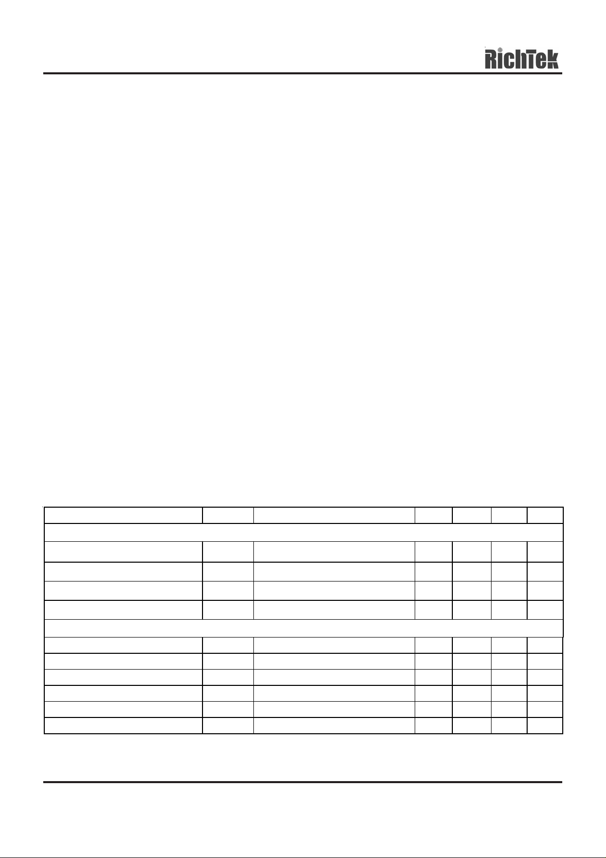
Electrical Characteristics
(V
= 12V, TA = 25°C, unless otherwise specified)
IN
Parameter Symbol Test Conditions Min Typ Max Units
Supply Input
Power Supply Voltage VCC -- 12 15 V
Power On Reset VCC 5.4 5.9 6.5 V
Power On Reset Hysteresis -- 0.3 -- V
Power Supply Current I
Soft Start
Soft Start Current ISS 8 10 15 μA
Oscillator
Free Running Frequency f
Frequency Variation -15 -- 15 %
Frequency Range 50 300 1000 kHz
Maximum Duty Cycle 70 75 80 %
VSS = 0V -- 10 -- mA
VCC
RT = 33kΩ 255 300 345 kHz
OSC
To be continued
DS8805-01 November 2005www.richtek.com
4

Parameter Symbol Test Conditions Min Typ Max Units
Reference Voltage
Preliminary
RT8805
Feedback Voltage VFB V
= 0.8V 0.784 0.8 0.816 V
FB
Error Amplifier
DC Gain 60 70 -- dB
Gain-Bandwidth Product GBW
Trans-conductance GM
MAX Current (Source & Sink)
V
I
COMP
C
LOAD
R
LOAD
COMP
= 5pF
= 20kΩ
= 2.5V
6 10 -- MHz
600 660 --
300 360 --
μA/V
μA
Current Sense GM Amplifier
OC
V
PHASE
R
IMAX
= 33kΩ
-- -220 -- mV
Gate Driver
Maximum Upper Drive Source I
Upper Drive Sink R
Maximum Lower Drive Source I
Lower Drive Sink R
UGATE(MAX)
UGATE
LGATE(MAX)
LGATE
BOOT − PHASE = 12V 1 -- -- A
V
= 1V -- 3.5 7 Ω
UGATE
PVCC = 12V 1 -- -- A
V
= 1V -- 2 4 Ω
LGATE
Protection
Under Voltage Protection 0.55 0.6 0.65 V
Power Sequence
Power Good Threshold 3.4 3.7 4 V
Power Good Sink Capability (4mA) -- 0.05 0.2 V
Note 1. Stresses listed as the above "Absolute Maximum Ratings" may cause permanent damage to the device. These are for
stress ratings. Functional operation of the device at these or any other conditions beyond those indicated in the
operational sections of the specifications is not implied. Exposure to absolute maximum rating conditions for extended
periods may remain possibility to affect device reliability.
Note 2. Devices are ESD sensitive. Handling precaution recommended.
Note 3. The device is not guaranteed to function outside its operating conditions.
Note 4. θ
is measured in the natural convection at TA = 25°C on a low effective thermal conductivity test board of
JA
JEDEC 51-3 thermal measurement standard.
DS8805-01 November 2005 www.richtek.com
5

RT8805
Preliminary
Typical Operating Characteristics
Phase Loading vs. Output Loading
30
Low-Side : IPD06N03
High-Side : IPD09N03
25
20
15
10
PHASE2
PHASE1
Phase Loading (A)
5
0
5 101520253035404550
Output Loading (A)
F
vs. Temperature
306
304
302
OSC
RRT = 33k
0.7945
0.7935
0.7925
(V)
REF
0.7915
V
0.7905
0.7895
V
vs. Temperature
REF
0.794
0.793
0.792
0.791
0.79
-40 -25 -10 5 20 35 50 65 80 95 110 125
Temp erature
(°C)
Dead Time
Low-Side : IPD06N03
High-Side : IPD09N03
UGATE
No Load
(kHz)
300
OSC
F
298
296
294
V
OUT
(100mV/Div)
I
L
(10A/Div)
SS
(2V/Div)
-40 -25 -10 5 20 35 50 65 80 95 110 125
Temp erature
(°C)
OCP
Short then Start up, CSS = 0.1μF
(5V/Div)
V
OUT
(1V/Div)
SS
(5V/Div)
I
L
(20A/Div)
UGATE
(20V/Div)
PHASE
LGATE
UGATE-PHASE
Time (100ns/Div)
OCP
Start up then Short, CSS = 0.1μF
Time (25ms/Div)
Time (25ms/Div)
DS8805-01 November 2005www.richtek.com
6

Preliminary
RT8805
V
OUT
(1V/Div)
UGATE
(20V/Div)
LGATE
(10V/Div)
I
L
(5A/Div)
Power Off
I
= 3A
OUT
Time (100μs/Div)
Short Pulse
Low-Side : IPD06N03
High-Side : IPD09N03
UGATE
UGATE-PHASE
During Soft Start
PHASE
LGATE
V
OUT
(1V/Div)
UGATE
(20V/Div)
LGATE
(10V/Div)
I
L
(5A/Div)
V
OUT
(500mV/Div)
UGATE
(10V/Div)
Power On
No Load
Time (1ms/Div)
Shutdown by SS Pin
No Load
(5V/Div)
V
OUT
(1V/Div)
LGATE
(10V/Div)
UGATE
(10V/Div)
SS
(1V/Div)
Time (100ns/Div)
Start Up by SS Pin
No Load, CSS = 0.1μF
Time (5ms/Div)
LGATE
(10V/Div)
V
OUT
(20mV/Div)
SS
(2V/Div)
LGATE
(10V/Div)
UGATE
(1V/Div)
Time (100μs/Div)
UVP
VIN = 0V, CSS = 0.1μF
Time (50ms/Div)
DS8805-01 November 2005 www.richtek.com
7

RT8805
Applications Information
Preliminary
Power On Reset
RT8805 operates with input voltage at VCC pin ranging
from 5.9V to 15V. An internal linear regulator regulates
the input voltage to 5V for internal control circuit use. The
POR (power on reset) circuitry monitors the supply voltage
to make sure the supply voltage is high enough for RT8805
normal work. When the regulated power exceeds 4.2V
typically, the RT8805 releases the reset state and works
according to the setting. Once the regulated voltage is
lower than 4.0V, POR circuitry resets the chip. Hysteresis
between the rising and falling thresholds assure that once
enabled, the RT8805 will not inadvertently turn off unless
the bias voltage drops substantially (see Electrical
Specifications).
Enable, Soft Start and Power Good
Once POR releases, the RT8805 begins its soft start cycle
as shown in Figure 1. A 10μA source current charges the
capacitor CSS connected to SS to control the soft start
behavior of RT8805. During soft start, SS voltage increases
linearly and clamps the error amplifier output. Duty cycle
and output voltage increase accordingly. The soft start
limits inrush current from input capacitors.
The RT8805 regards SS pin voltage higher than 3.7V as
the end of soft start cycle. Then RT8805 trip PGOOD to
high impedance if no fault occurs indicating power good.
The SS pin also act as the timer during OCP and UVP
hiccup as described in the later sections.
VDD
POR
SS
SSH
> 0.6V
FB
PGOOD
> 3.7V
Figure 1. Power Sequence
Frequency setting
The converter switching frequency is programmed by
connecting a resistor from the RT pin to GND. Figure 2
illustrates switching frequency vs. RRT.
Switching Frequency vs. RT Resistance
1200
1000
800
600
400
200
Switching Frequency (kHz)
0
0 20 40 60 80 100
RT Resistance (k )
Figure 2. Switching Frequency vs. R
(kΩ)
RT.
Voltage Control
The voltage control loop consists of error amplifier,
multiphase pulse width modulator, drivers and power
components. As conventional voltage mode PWM
controller, the output voltage is locked at the positive input
of error amplifier and the error signal is used as the control
signal of pulse width modulator. The PWM signals of
different channels are generated by comparison of EA
output and split-phase sawtooth wave. Power stage
transforms VIN to output by PWM signal on-time ratio.
Current Sensing Setting
RT8805 senses the current of low side MOSFET in each
synchronous rectifier when it is conducting for channel
current balance and OCP detecting. The multiplexer and
sensing GM amplifier converts the voltage on the sense
component (can be a sense resistor or the R
DS(ON)
of the
low side MOSFET) to current signal into internal circuit
(see Figure 3).
DS8805-01 November 2005www.richtek.com
8

Preliminary
PHASE1
PHASE2
RAMP2RAMP1
Current
Balance
OCP
IMAX
CLK2CLK1
S/H
OC
Figure 3. Current Sensing Loop
The sensing circuit gets IX = I
L(S/H)
x R
local feedback. IX is sampled and held just before low side
MOSFET turns off (See Figure 4). Therefore,
I
X(S/H)
T
OFF
SW
(S/H)
X
= I
=
=
L(S/H)
II
L(AVG)L(S/H)
⎡
⎢
⎣
200kHzF
⎡
⎢
⎢
⎢
⎢
⎣
x R
−
V
II
L(AVG)
DS(ON)
VV
IN
DS(ON)
V
OUTIN
−=
x GM
T
OFFOUT
,
2
s,5
μ
VV
−
⎛
×
⎜
⎝
OUTIN
V
IN
V
L
⎤
⎥
⎦
OUT
×−=
×
2L
GMR
××
DS(ON)
⎞
×
⎟
⎠
MUX
-
GM
+
x GM by
⎤
s5
μ
⎥
⎥
⎥
⎥
⎦
RT8805
Current Balance
RT8805 senses the voltage drop of the low-side MOS and
translates this to control the ramp signal. We can see
that the voltage signal finally injected to channel one is
proportional to (I
(I
- IL1). In steady state and current balance situation,
L2
there is no sensed signal injected into the ramp.
If IL1 > IL2, the ramp bottom of channel 1 will be lifted up
and decreased the duty of UGATE1. On the other hand,
the ramp bottom of channel 2 will be pulled low to increase
the duty of UGATE2. Finally, the loop will be back to the
balance state through above mentioned negative feedback
scheme. Figure 5 shows this scheme.
-
V
REF
RAMP2
RAMP1
COMP
+
1
−
2
V
CSO1
= k x V
- IL2). Channel two is proportional to
L1
V
IN2
Logic
Driver
k2 = k x R
= k2 x I
Logic
Driver
k1 = k x R
&
ON2
L2
&
ON1
= k x V
ON2
V
IN1
= k1 x I
V
L1
ON1
+
-
CSO2
+
-
Figure 5. Current Balance
V
V
I
L2
ON2
I
L1
ON1
L2
L1
V
OUT
CL
RL
Falling Slope = V
Inductor Current
OUT
/L
I
L(S/H)
I
L
I
L(AVG)
Gate control
a. Before SS signal reach the valley of the ramp voltage,
UGATE and LGATE will be off.
b. If SS pin is pulled down 0.4V, UGATE and LGATE will
be off.
High Side MOSFET Gate Signal
c. UV protect function caused by FB < 0.6V and SS >
3.7V, and controller will trigger Always Hiccup Mode.
d. When OC function occurs and SS > 3.7V, a constant
current of 10μA starts to discharge the capacitor
Low Side MOSFET Gate Signal
connected to SS pin right away. When OC occurs,
UGATE and LGATE will be off. When the voltage at the
Figure 4. Inductor Current and Gate signals
capacitor connected to SS pin pass about 0.4V, a
constant current of 10μA starts to charge the capacitor.
The PWM signal is enable to pass to UGATE and
DS8805-01 November 2005 www.richtek.com
9

RT8805
Preliminary
LGATE. OCP function monitors both channels, either
one can activate OCP. If the OC protection occurs three
times, OCSD (Over Current Shut Down) will be activated
and shut down the chip.
e. When fault conditions occur or SS < 0.4V, the current
sense function will be disabled.
Power Good
PGOOD goes high when soft-start voltage > 3.7V, and no
fault conditions.
Feedback Loop Compensation
The RT8805 is a voltage mode controller ; the control
loop is a single voltage feedback path including an error
amplifier and PWM comparator. In order to achieve fast
transient response and accurate output regulation, an
adequate compensator design is necessary. The goal of
the compensation network is to provide adequate phase
margin (greater than 45 degrees) and the highest 0dB
crossing frequency. To manipulate loop frequency response
under its gain crosses over 0dB at a slope of -20dB/
decade.
1) Modulator Frequency Equations
RT8805 is a voltage mode buck converter using the high
gain error amplifier with transconductance (OTA,
Operational Transconductance Amplifier), as Figure 6
shown.
The Transconductance:
ΔI
GM =
Δ VM = (EA+) - (EA-) ; Δ I
OUT
ΔV
M
EA+
EA-
= E/A output current.
OUT
V
OUT
+
GM
-
R
OUT
Figure 6. OTA Topology
This transfer function of OTA is dominated by a higher DC
gain and the output filter (L
pole frequency at FLC and a zero at F
OUT
and C
) with a double
OUT
. The DC gain of
ESR
the modulator is the input voltage (VIN) divided by the
peak to peak oscillator voltage V
RAMP
.
The first step is to calculate the complex conjugate poles
contributed by the LC output filter.
The output LC filter introduces a double pole, 40dB/decade
gain slope above its corner resonant frequency, and a total
phase lag of 180 degrees. The resonant frequency of the
LC filter expressed as follows:
F
P(LC)
=
π
1
CL2
××
OUTOUT
The next step of compensation design is to calculate the
ESR zero. The ESR zero is contributed by the ESR
associated with the output capacitance. Note that this
requires that the output capacitor should have enough ESR
to satisfy stability requirements. The ESR zero of the
output capacitor expressed as follows:
F
Z(ESR)
=
1
ESRC2
OUT
××
π
2) Compensation Frequency Equations
The compensation network consists of the error amplifier
and the impedance networks ZC and ZF as Figure 7 shown.
V
REF
V
OUT
R1
FB
+
GM
-
R
F
C2
R2
C1
V
COMP
Figure 7. Compensation Loop
=
F
Z1
=
F
P1
=
F
P2
1
π
××
C2R22
1
π
××
C1R12
1
×
C2C1
⎛
××
π
R22
⎜
⎝
⎞
⎟
+
C2C1
⎠
Figure 8 shows the DC-DC converter's gain vs. frequency.
The compensation gain uses external impedance networks
ZC and ZF to provide a stable, high bandwidth loop. High
crossover frequency is desirable for fast transient
response, but often jeopardize the system stability. In
order to cancel one of the LC filter poles, place FZ1 before
the LC filter resonant frequency. In the experience, place
FZ1 at 10% LC filter resonant frequency. Crossover
frequency should be higher than the ESR zero but less
than 1/5 of the switching frequency. The FP2 should be
place at half the switching frequency.
10
DS8805-01 November 2005www.richtek.com

Preliminary
80
80
60
40
40
20
0
0
Modulator
Gain (d B)
-20
-40
-40
-60
-60
10Hz 100Hz 1.0KHz 10KHz 100KHz 1.0MHz
10 100 1k 10k 100k 1M
vdb(vo) vdb(comp2) vdb(lo)
There is another type of compensation called Type 3
compensation that adds a pole-zero pair to the Type 2
network. It's used to compensate output capacitor whose
ESR value is much lower (pure MLCC or OSCON
Capacitors).
As shown in Figure 9, to insert a network between V
and FB in the original Type 2 compensation network can
result in Type 3 compensation. Figure 10 shows the
difference of their AC response. Type 3 compensation has
an additional pole-zero pair that causes a gain boost at
the flat gain region. But the gain boosted is limited by the
ratio (R1+R4)/R4; if R3 << R4.
V
OUT
Loop Gain
Gain
Frequency
Frequency (Hz)
Figure 8. Type 2 Bode Plot
C3
R3
R1
FB
R4
+
-
GM
Compensation
Gain
C2
R2
C1
V
COMP
OUT
RT8805
Type 3 will induce three poles and two zeros.
Zeros :
F
=
Z1
F
=
Z2
Poles :
=
F
P1
=
F
P2
=
F
P3
which is in the origin.
We recommend FZ1 placed in 0.5 x F
F
; FP1 placed in F
P(LC)
Figure 11 shows Type 3 Bode Plot.
60
40
20
0
dB
-20
-40
-60
-80
1
C2R22
××
π
1
C3R3)R12
(
π
×+×
1
×
C2C1
π
⎜
⎝
⎛
××
R22
⎞
⎟
+
C2C1
⎠
1
××
π
2
π
C3R32
1
⎛
×
⎜
+
⎝
;
××
C1R3R1
⎞
⎟
R3R1
⎠
; FZ2 placed in
P(LC)
and FP2 placed in 0.5 x FSW.
ESR
Loop Gain
Compensation Gain
Gain
Modulator Gain
234567
Log Frequency
Figure 9. Additional Network of Type 3 Compensation
(Add between V
and FB)
OUT
Figure 11. Type 3 Bode Plot
Protection
F
P3
Add Type 3 compensation
F
Z1
Original Type 3 compensation
F
Z2
F
P1
Pole
F
P2
Figure 10. AC Response Curves of Type 2 and 3
DS8805-01 November 2005 www.richtek.com
OCP
The RT8805 uses “ Cycle by Cycle” current comparison.
The over current level is set by IMAX pin. When OC
function occurs and SS > 3.7V, a constant current of 10μA
starts to discharge the capacitor connected to SS pin
right away. When OC occurs, UGATE and LGATE will be
off.
11

RT8805
Preliminary
When the voltage at the capacitor connected to SS pin
pass about 0.4V, a constant current of 10μA starts to
charge the capacitor. The PWM signal is enabled to pass
to the UGATE and LGATE. OCP function monitors both
channels, either one can activate OCP. If the OC protection
occurs three times, the chip will shut down and the state
will only be released by POR.
RT8805 uses an external resistor R
to set a
IMAX
programmable over current trip point. OCP comparator
compares each inductor current with this reference current.
RT8805 uses hiccup mode to eliminate fault detection of
OCP or reduce output current when output is shorted to
ground. The OCP comparator compares the difference
between IX and I
.
IMAX
OCP Comparator
I
IMAX
I
X
+
-
For example:
UVP
VIN = 0V
V
OUT
(20mV/Div)
SS
(2V/Div)
LGATE
(10V/Div)
UGATE
(1V/Div)
Time (50ms/Div)
Figure 12. UVP (Always Hiccup Mode)
OTP
Monitor the temperature near the driver part within the
chip. Shutdown the chip when OTP (Typical trip point :
170°C).
From Electrical Specifications : R
V
Assume Low side MOSFET R
Get the OCP setting current is =73A per PHASE
PHASE
= -220mV
DS(ON)
220mV
= 33kΩ
IMAX
= 3mΩ.
Ω3m
(the valley of inductor's current).
Change the setting current which you want from 73A per
PHASE to 50A per PHASE.
Following below steps:
1. Calculate phase voltage. If Low side MOSFET
R
= 3mΩ, V
DS(ON)
IMAX_new
IMAX_new
PHASE_new
-220mV
R 2.
V
PHASE_new
Ω=
48.4k R
= -150mV.
Ω×=
33k
UVP
By detecting voltage at FB pin when SS > 3.7V. If
FB < 0.6V, the chip will trigger the always Hiccup mode
and a constant current source 10μA starts to charge
capacitor at SS pin when SS pass 0.4V and discharge
Css when SS > 3.7V. As Figure 12 shown.
General Design Guide
This design guide is intended to provide a high-level
explanation of the steps necessary to create a multi-phase
power converter. It is assumed that the reader is familiar
with many of the basic skills and techniques referenced
below.
Power Stages
Designing a multi-phase converter is to determine the
number of phases. This determination depends heavily
on the cost analysis which in turn depends on system
constraints that differ from one design to the next.
Principally, the designer will be concerned with whether
components can be mounted on both sides of the circuit
board, whether through-hole components are permitted,
the total board space available for power-supply circuitry,
and the maximum amount of load current. Generally
speaking, the most economical solutions are those in
which each phase handles between 20 to 25 A (One Upper
and one Lower MOSFET). All surface-mount designs will
tend toward the lower end of this current range.
If through-hole MOSFETs and inductors can be used,
higher per-phase currents are possible. In cases where
12
DS8805-01 November 2005www.richtek.com

Preliminary
RT8805
board space is the limiting constraint, current can be
pushed as high as 40A per phase, but these designs
require heat sinks and forced air to cool the MOSFETs,
inductors and heat dissipating surfaces.
MOSFET s
The choice of MOSFETs depends on the current each
MOSFET will be required to conduct, the switching
frequency, the capability of the MOSFETs to dissipate
heat, and the availability and nature of heat sinking and
air flow.
Package Power Dissipation
When choosing MOSFETs it is important to consider the
amount of power being dissipated in the integrated drivers
located in the controller. Since there are a total of two
drivers in the controller package, the total power dissipated
by both drivers must be less than the maximum allowable
power dissipation for the VQFN package. Calculating the
power dissipation in the drivers for a desired application
is critical to ensure safe operation. Exceeding the
maximum allowable power dissipation level will push the
IC beyond the maximum recommended operating junction
temperature of 125°C. The maximum allowable IC power
dissipation for the 3x3 VQFN package is approximately
1.47W at room temperature.
According below equations at two phases operation, it’s
clear to describe that the junction temperature of the chip
is directly proportional to the total C
and C
PD = ( C
) of all external MOSFETs.
LGATE
x V
UGATE
BOOT-PHASE
2
x f ) + ( C
(including C
ISS
x V
LGATE
CC
UGATE
2
x f ) +
χ
operated under or over maximum (~125°C) operation
rating.
Layout Considerations
Layout is very important in high frequency switching
converter design. If designed improperly, the PCB could
radiate excessive noise and contribute to the converter
instability.
First, place the PWM power stage components. Mount
all the power components and connections in the top layer
with wide copper areas. The MOSFETs of Buck, inductor,
and output capacitor should be as close to each other as
possible. This can reduce the radiation of EMI due to the
high frequency current loop. If the output capacitors are
placed in parallel to reduce the ESR of capacitor, equal
sharing ripple current should be considered. Place the
input capacitor directly to the drain of high-side MOSFET.
In multi-layer PCB, use one layer as power ground and
have a separate control signal ground as the reference of
the all signal. To avoid the signal ground is effect by noise
and have best load regulation, it should be connected to
the ground terminal of output. Furthermore, follows below
guidelines can get better performance of IC :
1. A multi-layer printed circuit board is recommended.
2. Use a middle layer of the PC board as a ground plane
and making all critical component ground connections
through vias to this layer.
3. Use another solid layer as a power plane and break this
plane into smaller islands of common voltage levels.
4. Keep the metal running from the PHASE terminal to
the output inductor short.
TJ = TA + ( θ
(χ is the minor factor and could be ignored)
For example, according to the application we evaluated
on board, the C
in parallel), V
frequency = 300kHz.
≈
PD 1nF x 122 x 300kHz + 2 x 5nF x 122 x 300kHz =
475mW / PHASE
x PD )
JA
UGATE
= 12V, V
CC
= 1nF, C
BOOT-PHASE
= 5nF (dual MOSFETs
LGATE
= 12V, and operation
5. Use copper filled polygons on the top and bottom circuit
layers for the phase node.
6. The small signal wiring traces from the LGATE and
UGATE pins to the MOSFET gates should be kept
short and wide enough to easily handle the several
Amperes of drive current.
7. The critical small signal components include any bypass
capacitors, feedback components, and compensation
components. Position those components close to their
TJ = 30°C+ 68°C/W x 0.475W x 2 = 94.6°C
That means the junction temperature is most likely to be
DS8805-01 November 2005 www.richtek.com
pins with a local GND connection, or via directly to the
ground plane.
13

RT8805
Preliminary
8. RT and R
pin respectively, and their GND return should be short,
and kept away from the noisy MOSFET GND.
9. Place the compensation components close to the FB
and COMP pins.
10. The feedback resistors for both regulators should also
be located as close as possible to the relevant FB pin
with vias tied straight to the ground plane as required.
11. Minimize the length of the connections between the
input capacitors, CIN and the power switches by placing
them nearby.
12. Position both the ceramic and bulk input capacitors
as close to the upper MOSFET drain as possible, and
make the GND returns (From the source of lower
MOSFET to VIN, C
13. Position the output inductor and output capacitors
between the upper MOSFET and lower MOSFET and
the load.
resistors should be near the RT and R
IMAX
, GND) short.
VIN
IMAX
14. AGND should be on the clearer plane, and kept away
from the noisy MOSFET GND.
14
DS8805-01 November 2005www.richtek.com

Outline Dimension
Preliminary
RT8805
D
E
A
A3
A1
D2
e
SEE DETAIL A
1
E2
b
L
1
2
1
2
DETAIL A
Pin #1 ID and Tie Bar Mark Options
Note : The configuration of the Pin #1 identifier is optional,
but must be located within the zone indicated.
Dimensions In Millimeters Dimensions In Inches
Symbol
Min Max Min Max
A 0.800 1.000 0.031 0.039
A1 0.000 0.050 0.000 0.002
A3 0.175 0.250 0.007 0.010
b 0.180 0.300 0.007 0.012
D 2.950 3.050 0.116 0.120
D2 1.300 1.750 0.051 0.069
E 2.950 3.050 0.116 0.120
E2 1.300 1.750 0.051 0.069
e 0.500 0.020
L 0.350 0.450
RICHTEK TECHNOLOGY CORP .
Headquarter
5F, No. 20, Taiyuen Street, Chupei City
Hsinchu, Taiwan, R.O.C.
Tel: (8863)5526789 Fax: (8863)5526611
0.014 0.018
V-Type 16L QFN 3x3 Package
RICHTEK TECHNOLOGY CORP .
Taipei Office (Marketing)
8F-1, No. 137, Lane 235, Paochiao Road, Hsintien City
Taipei County, Taiwan, R.O.C.
Tel: (8862)89191466 Fax: (8862)89191465
Email: marketing@richtek.com
DS8805-01 November 2005 www.richtek.com
15

 Loading...