

Page 1
High Voltage 4 Channel LED Driver
RT8560A
General Description
The RT8560A is a 60V 4-channel LED driver capable of
delivering 30mA to ea ch cha nnel with 15 LEDs (3.6V per
diode) total 60 LEDs with one driver. The R T8560A is a
current mode boost converter opearated at 1MHz switching
frequency , wide V
on-chip current switch is rated at 1.5A.
The PWM output voltage loop selects and regulates the
LED pin with the highest voltage string to 0.9V allowing
voltage mismatches between LED strings. The RT8560A
automatically detects and disconnects a ny unconnected
and/or broken strings during operation from PWM loop to
prevent V
OUT
The 3% matched LED currents on all cha nnels are simply
programmed with a resistor or a current sink. Both a nalog
dimming and digitally controlled PWM dimming are
supported by RT8560A. Analog dimming is linearly
controlled by an external voltage. With a n on-chip output
clampping a mplifier a nd a 200kΩ resistor , PWM dimming
signal is easily low-pass filtered to an analog dimming
signal with one external capacitor for noise-free PWM
dimming. A very high contrast ratio true digital PWM
dimming can be achieved by driving EN pin to PWM
shutdown the chip or by driving ACTL pin.
range covers from 6V to 40V and the
IN
from over voltage.
Features
zz
High V oltage : VIN up to 40V , V
z
zz
up to 60V , Driving
OUT
up to 60 x 3.6V LEDs (15 each channel)
zz
z Channel Current Programmabe 4mA to 30mA and
zz
Matched to 3% Accuracy
zz
z Current Mode PWM 1MHz Boost Converter
zz
zz
z Easy Analog and Digital Dimming Control
zz
zz
z Programmable Soft Start
zz
zz
z Automatic Detecting Unconnected and/or Broken
zz
Channel
zz
z Programmable Over Voltage Protection
zz
zz
z Disconnects LED in Digital Dimming : Providing
zz
High Accuracy Digital Dimming by PWM at ACTL
Pin or EN Pin
zz
z V
Under Voltage Lockout
zz
IN
zz
z Over Temperature Protection
zz
zz
z Current Limiting Protection
zz
zz
z Small 20-Lead WQFN Package
zz
zz
z RoHS Compliant and Halogen Free
zz
Applications
z UMPC and Notebook Computer Backlight
z GPS, Portable DVD Backlight
z Desk Lights and Room Lighting
Other protecting features include programmable PWM
output over voltage protection, LED curren limit, PWM
switch current limit and thermal shutdown. The R T8560A
is packaged with a tiny footprint package of WQFN-20L
4x4 packages.
Ordering Information
RT8560A
Package Type
QW : WQFN-20L 4x4 (W-Type)
Lead Plating System
G : Green (Halogen Free and Pb Free)
Note :
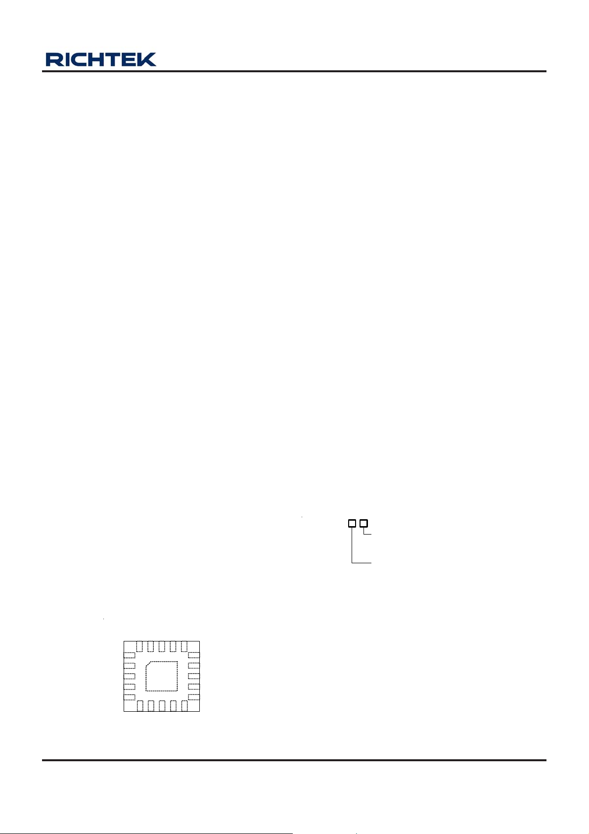
Pin Configurations
(TOP VIEW)
GND
GND
20 19 18 1617
1
GND
2
GND
3
GND
SW
SW
GND
4
5
7
8910
6
VCC2
VCC1
LED2
LED1
21
ACTL
RISET
LED3
15
LED4
14
VC
13
SS
12
OVP
11
EN
DCTL
Richtek products are :
` RoHS compliant and compatible with the current require-
ments of IPC/JEDEC J-STD-020.
` Suitable for use in SnPb or Pb-free soldering processes.
Marking Information
For marking information, contact our sales representative
directly or through a Richtek distributor located in your
area.
WQFN-20L 4x4
DS8560A-01 April 2011 www.richtek.com
1
Page 2
RT8560A
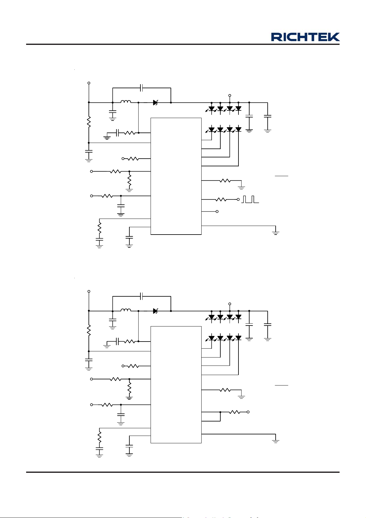
Typical Application Circuit
V
IN
6V to 40V
L
10µH
C
VIN
10µF
R
VCC1
10
C
1µF
V
OUT
V
IN
VCC1
R
R
1.8k
VCC2
10
VC
C
VC
3.9nF
C2
R1
5V
R4
C
VCC2
1µF
R3
1k
C
OUT3
1µF
R2
C1
0.1µF
4, 5
11
12
14
13
7
6
D
SW
VCC1
EN
OVP
VCC2
VC
SS
15 LED String
RT8560A
V
OUT
60V MAX
:
:
:
:
:
:
:
:
:
:
:
:
18
LED1
17
LED2
16
LED3
15
LED4
RISET
ACTL
DCTL
GND
R
ISET
5.36k
8
R5
1k
9
10
PWM Signal
1, 2, 3, 19, 20, Exposed Pad (21)
:
:
C
OUT1
:
:
I = 20mAR×
LED
C
OUT2
5.36k
ISET
Figure 1. 1MHz, 20mA Full Scale Current Digital PWM Di mming Control
V
IN
6V to 40V
R
10
C
1µF
V
OUT
V
IN
VCC1
VCC1
R
VCC2
10
R
VC
1.8k
C
VC
3.9nF
C2
5V
R1
10µH
C
VIN
10µF
L
R4
C
VCC2
1µF
R3
1k
R2
C
OUT3
1µF
4, 5
C1
0.1µF
11
12
14
13
7
6
D
SW
VCC1
EN
OVP
VCC2
VC
SS
15 LED String
RT8560A
V
OUT
60V MAX
:
:
:
:
:
:
:
:
:
:
:
:
18
LED1
17
LED2
16
LED3
15
LED4
RISET
ACTL
DCTL
GND
R
ISET
5.36k
8
R5
9
1k
10
1, 2, 3, 19, 20, Exposed Pad (21)
:
:
C
OUT1
:
:
I = 20mAR×
LED
Analog
Dimming
C
OUT2
5.36k
ISET
Figure 2. 1MHz, 20mA Full Scale Current An alog Dimming Control
DS8560A-01 April 2011www.richtek.com
2
Page 3
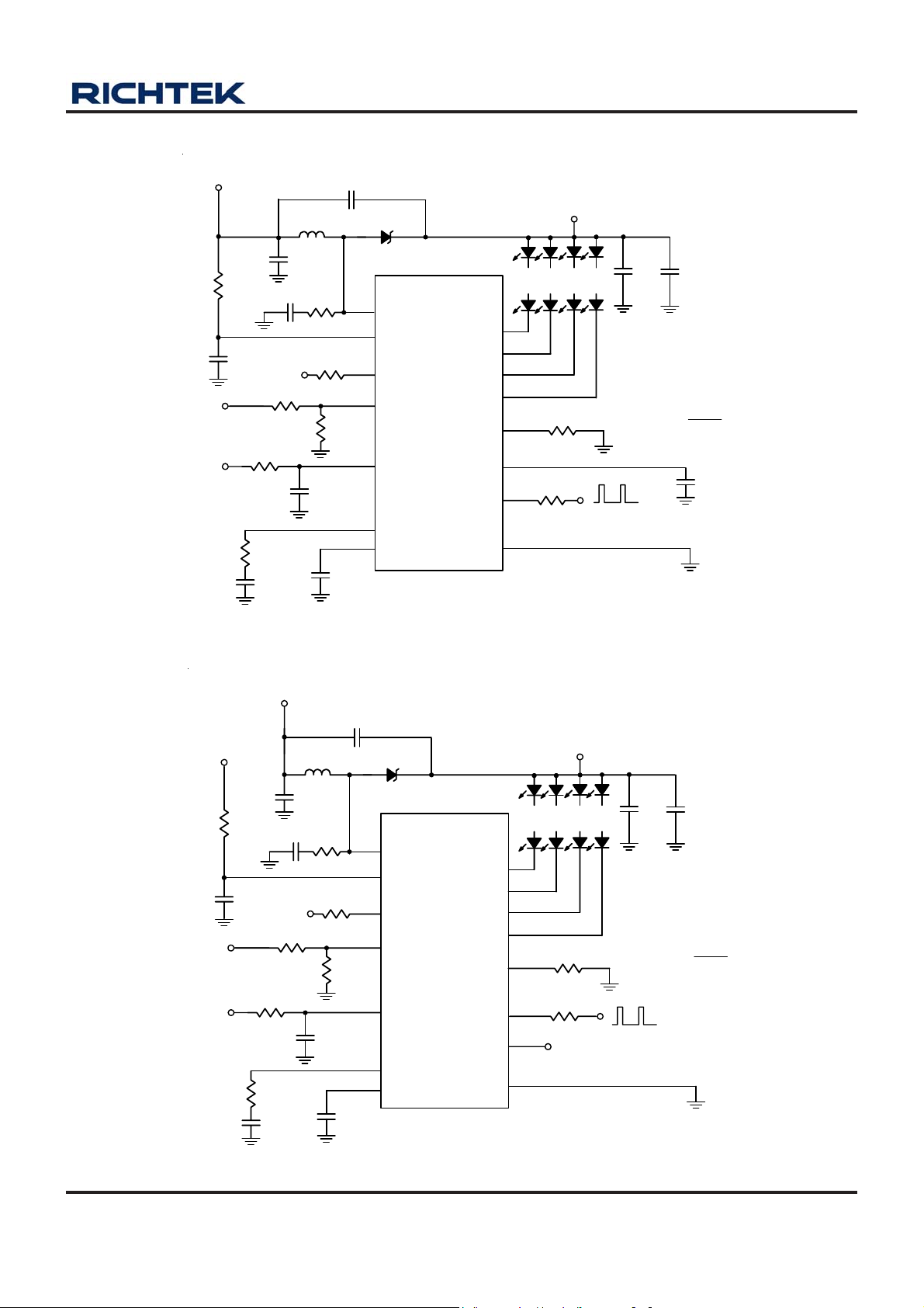
V
IN
6V to 40V
R
10
C
1µF
V
OUT
V
IN
VCC1
VCC1
R
VCC2
10
R
VC
1.8k
C
3.9nF
VC
C3
5V
R1
10µH
C
VIN
10µF
L
R4
C
1µF
C
R3
1k
R2
VCC2
C1
0.1µF
OUT3
1µF
4, 5
11
12
14
13
7
6
D
SW
VCC1
EN
OVP
VCC2
VC
SS
15 LED String
RT8560A
V
OUT
60V MAX
:
:
:
:
:
:
:
:
:
:
:
:
18
LED1
17
LED2
16
LED3
15
LED4
RISET
ACTL
DCTL
8
9
10
R
ISET
5.36k
R5
1k
PWM Signal
1, 2, 3, 19, 20, Exposed Pad (21)
GND
:
:
C
OUT1
:
:
I = 20mAR×
LED
C
RT8560A
OUT2
5.36k
ISET
C2
0.1µF
Figure 3. 1MHz, 20mA Full Scale Current PWM to Analog Di mming Control
V
IN
V
AVDD
6V to 40V
R
10
V
OUT
V
IN
VCC1
C
VCC1
2.2µF
R
4V to 40V
C2
5V
R1
VCC2
10
R
VC
1.8k
C
VC
3.9nF
10µH
C
VIN
10µF
L
R4
C
VCC2
1µF
C
R3
1k
R2
C1
0.1µF
OUT3
1µF
4, 5
11
12
14
13
7
6
D
SW
VCC1
EN
OVP
VCC2
VC
SS
15 LED String
RT8560A
V
OUT
60V MAX
:
:
:
:
:
:
:
:
:
:
:
:
18
LED1
17
LED2
16
LED3
15
LED4
RISET
ACTL
DCTL
GND
R
ISET
5.36k
8
R5
1k
9
10
1, 2, 3, 19, 20, Exposed Pad (21)
:
:
C
OUT1
:
:
I = 20mAR×
LED
PWM Signal
C
OUT2
5.36k
ISET
Figure 4. Wide Range VIN Application by Connecting VCC1 to LCD Driver Power A V DD
DS8560A-01 April 2011 www.richtek.com
3
Page 4
RT8560A
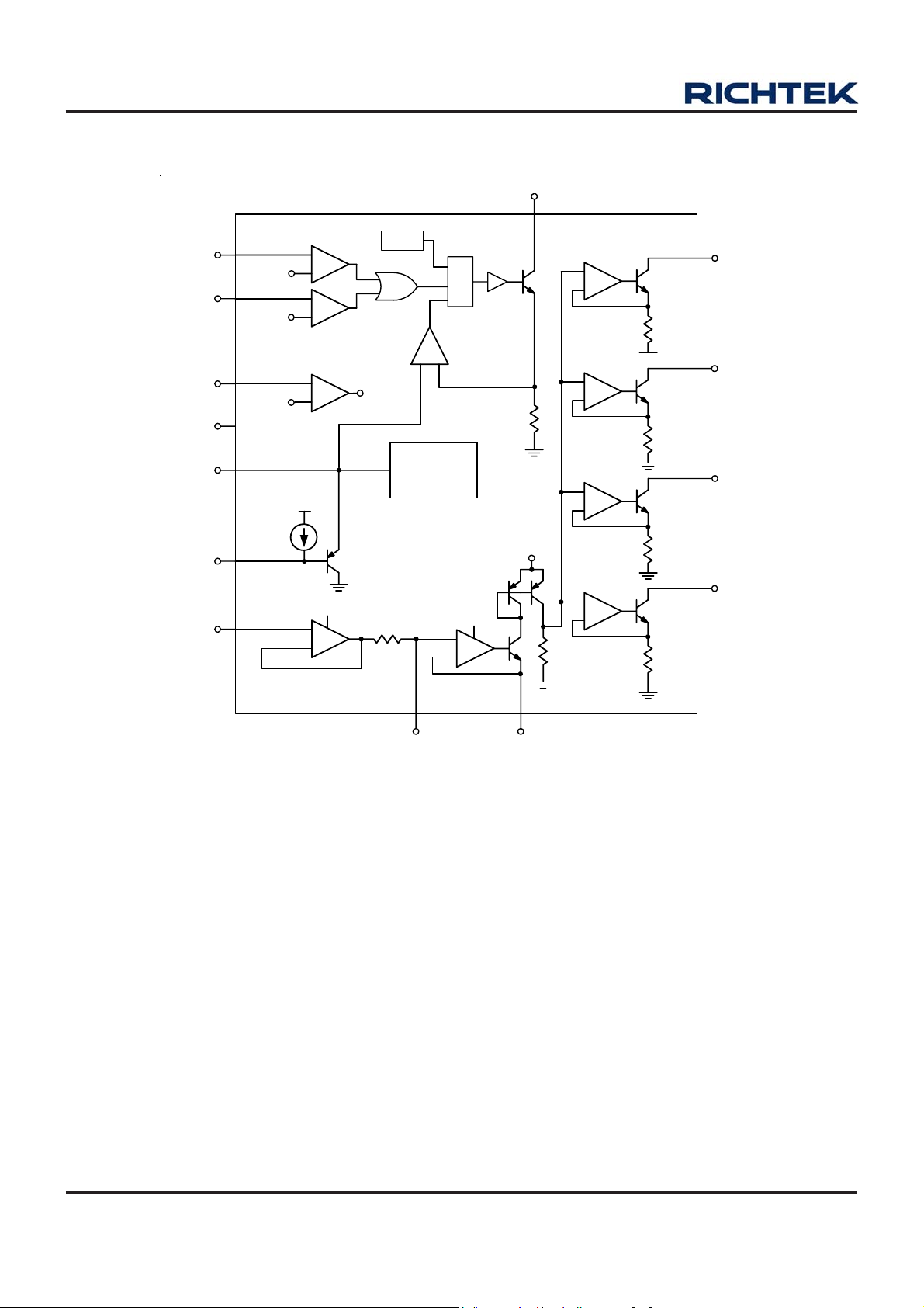
Function Block Diagram
SW
VCC1
OVP
EN
VCC2
VC
SS
DCTL
6.2V
2.5V
2V
6uA
+
+
-
+
1.2V
+
-
OSC
Shutdown
200k
S
R
R
+
-
V
OUT
Regulation
Unit
1.2V
+
-
+
LED1
-
LED2
+
-
LED3
+
-
5V
LED4
+
-
ACTL
RISET
DS8560A-01 April 2011www.richtek.com
4
Page 5
Functional Pin Description
Pin Numbe r Pin Name Pin Function
1, 2, 3, 19, 20,
21 (Exposed Pad)
4, 5 SW
6 VCC2
7 VCC1
8 RISET
GND
Ground pin of the chip. The exposed pad must be soldered to a large PCB
and connected to GND for maximum power dissipation.
PWM boost converter switch node.
Bipolar power switch base current supply. Typical beta of the power N PN
switch is approximately 70. VCC2 can be connected either to VCC1 or to a
separate lower voltage, as low as 3V, for better s ystem efficiency and/or
heat concern. A good bypass is necessary.
Power supply of the chip. For good bypass, a low ESR capacitor is required.
A resistor or a current from DAC on this pin programs the full LED current.
RT8560A
9 ACTL
10 DCTL
11 EN
12 OVP
13 SS
14 VC
18, 17, 16, 15
LED1, LED2,
LED3, LED4
Analog / Digi tal dimming co ntrol. When using anal og dimming,
I = 20mA for V 1.2V.
LED ACTL
By adding a 0.1uF filtering capacitor on ACTL pin, the PWM dimming signal
on DCTL pin will be averaged out and converte d into analog dimming signal
on ACTL pin.
Chip enable pin, when low chip is in shutdown mode.
Over voltage protection. PWM boost converter turns off when V
higher than 2.5V.
Soft start pin, a capacitor of at least 10nF is requi red for soft start.
PWM boost converter loop compensation node.
Channel 1 to Channel 4 LED current sink. Leave the pin unconnected if not
used.
5.36k
×≥
R
ISET
OVP
goes
DS8560A-01 April 2011 www.richtek.com
5
Page 6

RT8560A
Absolute Maximum Ratings (Note 1)
z Supply V oltage, VCC1, VCC2------------------------------------------------------------------------------------------ 42V
z SW Pin Voltage at Switching Off -------------------------------------------------------------------------------------- 65V
z LED1, LED2, LED3, LED4 Pin ----------------------------------------------------------------------------------------- 25V
z EN Pin Voltage ------------------------------------------------------------------------------------------------------------- 20V
z RISET Pin V oltage -------------------------------------------------------------------------------------------------------- 4V
z ACTL, DCTL, OVP , SS, VC Pins Voltage --------------------------------------------------------------------------- 8V
z Power Dissipation, P
WQFN-20L 4x4 ------------------------------------------------------------------------------------------------------------ 1.852W
z Package Thermal Re sistance (Note 2)
WQF N-20L 4x4, θJA------------------------------------------------------------------------------------------------------- 54°C/W
WQFN-20L 4x4, θJC------------------------------------------------------------------------------------------------------ 7°C/W
z Junction T emperature----------------------------------------------------------------------------------------------------- 150 °C
z Lead Temperature (Soldering, 10 sec.)------------------------------------------------------------------------------- 260°C
z Storage T emperature Range -------------------------------------------------------------------------------------------- −65°C to 150°C
z ESD Susceptibility (Note 3)
HBM (Human Body Mode) ---------------------------------------------------------------------------------------------- 2kV
MM (Ma chine Mode)------------------------------------------------------------------------------------------------------ 200V
@ TA = 25°C
D
Recommended Operating Conditions (Note 4)
z Supply Input V oltage, VCC1, VCC2 ---------------------------------------------------------------------------------- 6V to 40V
z Junction T emperature Range--------------------------------------------------------------------------------------------
z Ambient T emperature Range--------------------------------------------------------------------------------------------
−40°C to 125°C
−40°C to 85°C
Electrical Characteristics
(V
= 17V, T
CC1
V
UVLO Threshold V
CC1
Supply Current I
Shutdown Current I
EN
Threshold
ACTL
Threshold
EN Pin Input Current IEN VEN ≤ 5V -- - - 2 μA
LED Current P rogramming
LED Cur rent I
LED´s Current Matching
RISET Pin Voltage V
Input Current of ACTL I
= 25°C, unless otherwise specified)
A
Parameter Symbol Test Conditions Min Typ Max Unit
Logic-High Voltage V
Logic-Low Voltage
Logic-High Voltage V
Logic-Low Voltage
V
UVLO
VC ≤ 0.4V (Switching off) -- 4 7 mA
VCC1
VEN ≤ 0.7V -- 12 -- μA
SHDN
2 -- 5
EN_H
-- -- 0.8
V
EN_L
ACTL_H
V
ACTL_L
LED
RISET
ACTL
-- -- 0.15
R
0.3V ≤ V
Rising -- 5.5 5.95 V
CC1
2 -- 5
2V > V
V
ACTL
2V > V
V
ACTL
(I
(MAX)
ISET
> 0.7 V, R
LED
= 5.36kΩ,
ISET
>1.28V
> 0.7 V, R
LED
= 5.36kΩ,
ISET
>1.28V, Calc ulating
− I
= 5.36kΩ, V
/ I
(MIN)
ACTL
AVERAGE
ACTL
≤ 1.2V -- -- 2 μA
x 100%)
> 1.28V -- 1.21 -- V
19 20 21 mA
-- -- 3 %
To be continued
V
V
DS8560A-01 April 2011www.richtek.com
6
Page 7

RT8560A
Parameter Symbol Test Conditions Min Typ Max Unit
Threshol d of ACTL V
Input Current of DCTL I
LED Current Off -- 0.2 -- V
ACTL
0.3V ≤ V
DCTL
≤ 6V -- -- 1 μA
DCTL
PWM Boost Converte r
Switching Frequency 840 1000 1160 kHz
Maximum Duty Cycle -- 88 -- %
Minimum On Time -- 200 -- ns
Regulated V
Highest Voltag e LED Str ing -- 0 .9 -- V
LED
Amplifier gm GM -- 220 -- μA/V
Amplifier (gm) Output Current 2.4V > VC > 0.2V -- ±30 -- μA
VC Threshold PW M Switch Off -- 0.7 -- V
SW On Voltage ISW = 0.5A -- 0.4 -- V
SW Current Limit I
1.2 1.5 -- A
LIM
OVP & Soft Start
OVP Threshold V
OVP Input Current I
-- 2.5 -- V
OVP
V
OVP
≤ 2.5V -- -- 50 nA
OVP
Soft Start Current ISS VSS = 0V -- 7 -- μA
Note 1. Stresses listed as the above “Absolute Maximum Ratings” may cause permanent damage to the device. These are for
stress ratings. Functional operation of the device at these or any other conditions beyond those indicated in the
operational sections of the specifications is not implied. Exposure to absolute maximum rating conditions for extended
periods may remain possibility to affect device reliability.
Note 2. θ
Note 3. Devices are ESD sensitive. Handling precaution is recommended.
Note 4. The device is not guaranteed to function outside its operating conditions.
is measured in the natural convection at TA = 25°C on a high effective four layers thermal conductivity test board of
JA
JEDEC 51-7 thermal measurement standard. The case point of θ
is on the expose pad for the WQFN package.
JC
DS8560A-01 April 2011 www.richtek.com
7
Page 8
RT8560A
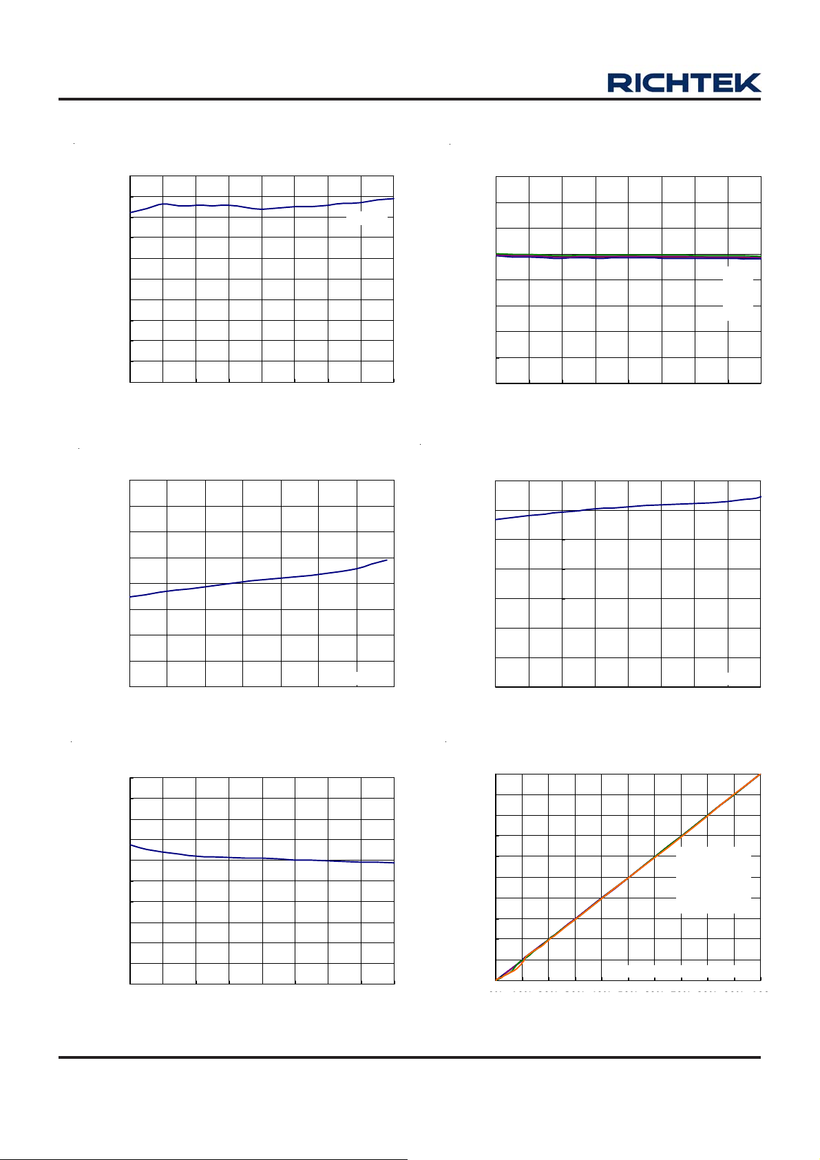
Typical Operating Characteristics
Efficiency vs. Input Voltage
100
90
80
70
60
50
40
Efficiency (%)
30
20
10
0
8 1216202428323640
Input Voltage (V)
LED Current v s . Te m perature
24
23
22
21
20
19
18
LED Current (mA)
17
16
-40 -15 10 35 60 85 110 135
Temperature
(°C)
60LEDs
V
= 12V
IN
LED Curre nt vs. Input Voltage
26
24
22
20
18
16
LED Current (mA)
14
12
10
8 1216202428323640
Input Volt age (V)
V
vs. Temperature
1.24
1.22
1.20
1.18
(V)
RISET
1.16
V
1.14
1.12
1.10
-40 -20 0 20 40 60 80 100 120
RISET
Temperature
(°C)
V
IN
LED1
LED2
LED3
LED4
= 12V
LED Curre nt v s. ACTL P WM Duty Cycle
20
18
16
14
12
10
8
6
LED Current (mA)
4
2
0
0% 10% 20% 30% 40% 50% 60% 70% 80% 90% 100
0 10 20 30 40 50 60 70 80 90 100
ACTL = 0V to 3V, V
Duty Cycle (%)
ACTL = 200Hz
ACTL = 1kHz
ACTL = 10kHz
ACTL = 20kHz
ACTL = 30kHz
IN
= 12V
%
(V)
RISET
V
V
vs . Input Voltage
1.25
1.24
1.23
1.22
1.21
1.20
1.19
1.18
1.17
1.16
1.15
8 1216202428323640
RISET
Inpu t Voltage (V)
DS8560A-01 April 2011www.richtek.com
8
Page 9
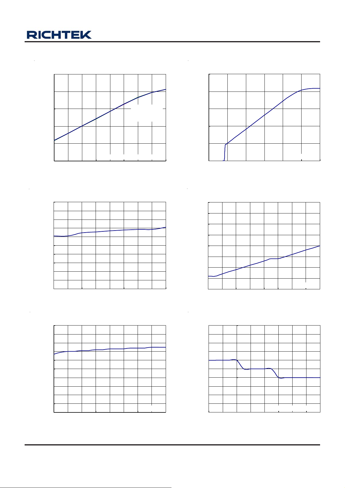
RT8560A
LED Current v s. DCTL PWM Duty Cycle
25
20
15
10
DCTL = 200Hz
DCTL = 1kHz
DCTL = 10kHz
LED Current ( m A)
5
0
20 30 40 50 60 70 80 90 100
DCTL = 0V to 3V, V
Dut y Cycle (% )
Frequency vs. Input Voltage
1.10
1.08
1.06
1.04
1.02
1.00
0.98
0.96
Frequency ( M H z)
0.94
0.92
0.90
8 1012141618202224
Inp ut Voltage (V)
IN
= 12V
LED Curre nt v s. ACTL Voltage
25
20
15
10
LED Current (mA)
5
V
0
0 0.25 0.5 0.75 1 1.25 1.5
IN
ACTL Volta ge ( V)
Shutdown Current vs. Input Voltage
40
35
30
25
20
15
10
Shutdown Current (uA)
5
V
0
8 1216202428323640
Inpu t Voltage (V)
EN
= 12V
= 0V
Switch Off Current vs. Input Voltage
5.0
4.9
4.8
4.7
4.6
4.5
4.4
4.3
4.2
Switch Off Current (mA)
4.1
4.0
8 1216202428323640
Inpu t Voltage (V)
VC = 0V
10
9
8
7
6
5
4
3
SS Current (uA)
2
1
0
-40 -20 0 20 40 60 80 100 120
SS Current vs. Temperature
V
= 12V, C
IN
Temperature
SS
(°C)
= 0.1uF
DS8560A-01 April 2011 www.richtek.com
9
Page 10

RT8560A
SS Current vs. Input Voltage
10
9
8
7
6
5
4
3
SS Current (uA)
2
1
0
81216202428323640
C
SS
Inpu t Voltage (V)
OVP Voltag e vs. Input Voltage
2.8
2.7
2.6
2.5
2.4
OVP Voltage (V)
2.3
= 0.1uF
OVP Voltage vs. Temperature
2.50
2.48
2.46
2.44
2.42
2.40
2.38
2.36
OVP Voltage (V)
2.34
2.32
2.30
-40 -20 0 20 40 60 80 100 120
Temperature
(°C)
Limit Current vs. Input Voltage
2.5
2.0
1.5
1.0
Limit Current ( A)
0.5
V
IN
= 12V
10
2.2
81216202428323640
Inp ut V o ltage (V)
ACTL Voltage vs. Temperature
0.40
0.35
0.30
0.25
0.20
0.15
ACTL Volt age (V)
0.10
0.05
0.00
-40 -20 0 20 40 60 80 100 120
Temperature
(°C)
V
IN
= 12V
0.0
V
EN
(2V/Div)
V
OUT
(20V/Div)
I
IN
(500mADiv)
8 101214161820222426283032
Inpu t Voltage (V)
Power On from EN
V
= 12V, C
IN
Time (5ms/Div)
DS8560A-01 April 2011www.richtek.com
= 0.1uF
SS
Page 11

RT8560A
V
IN
(5V/Div)
I
OUT
(50mA/Div)
Line Transient Response
V
= 10.8V to 13.2V, RISET = 4.8kΩ
IN
Time (50ms/Div)
V
IN
(5V/Div)
V
OUT
(20V/Div)
SW
(20V/Div)
OVP
V
= 12V, All LED Pin Open
IN
Time (2.5ms/Div)
DS8560A-01 April 2011 www.richtek.com
11
Page 12

RT8560A
Applications Information
The RT8560A is a current mode boost converter operated
at 1MHz to power up to 60 white LEDs with a
programmable current for uniform intensity. The part
integrates current sources, soft-start, and easy analog
and digital dimming control. The protection block provides
the circuitry for over-temperature, over-voltage and currentlimit protection features.
Input UVLO
The input operating voltage range of the RT8560A is 6V to
40V. An input capacitor at the VCC1 and VCC2 pin can
reduce ripple voltage. It is recommended to use a cera mic
10uF or larger cap acita nce as the in put cap acitor . This IC
provides an under voltage lockout (UVLO) function to
enhance the stability when startup. The UVLO threshold
of input rising voltage is around 5.5V .
Power Sequence
Please refer to the below Figure 5 and 7. The
recommended power-on sequence is that the PWM ready
before EN and/or VIN rea dy . If not, the Soft-Start function
will be disabled. As to power-off sequence, the EN/VIN
must be pulled low within 10ms to prevent “Hard-Start”
shown as Figure 7.
Abnormal Poweron sequence
UVLO
VIN
PWM
Power-on
sequence
Power-off
sequence
Power-on
sequence
VIN
PWM
EN
VOUT
Power-off
sequence
VIN must be turn ed
off early than EN and
PWM signal
Soft-Start
VIN must be
turned on late
than EN and
PWM signal
Abnormal Poweron sequence
UVLO
No Soft-Start
If PWM tu rns
on late
Figure 6. Power-On Sequence Control by VIN
EN/VIN
PWM
10ms
EN and/or VIN should be
pulled low once PWM pull low
for over 10ms
Figure 7. To Prevent “Hard-Start” Sequence
Soft Start
The RT8560A employs a soft start feature to limit the inrush
current. The soft-start circuit prevents the excessive inrush
current and input voltage droop. The soft-start time is
determined by cap acitor CSS connected to SS with a 7uA
constant current to charge CSS. The value of capacitor
CSS is user-defined to satisfy designer' requirement.
EN must be turned
off early than VIN
and PWM signal
EN
VOUT
EN must be turned
on late than VIN
and PWM signal
Soft-Start
Figure 5. Power-On Sequence Control by EN
12
No Soft-Start
If PWM turn s
on late
LED connection
The RT8560A equips 4 channel LED divers and each
channel supports up to 15 LEDs. The 4 LED strings are
connected from VOUT to pin 15, 16, 17 and 18
respectively. If one of the LED channel is not used, the
LED pin should be opened dire ctly .
Setting and Regulation of LED current
The LED current can be calculated by the following
equation :
I = 20mA
LED
5.36k
×
R
ISET
DS8560A-01 April 2011www.richtek.com
Page 13

RT8560A
Where,
V
is the voltage of the RISET pin (1.21V typ.) and the
RISET
R
is the resister between RISET pin and GND.
ISET
This setting is the reference for the LED current at LED14 and represents the sensed LED current for ea ch string.
The DC/DC converter regulates the LED current according
to the setting.
Brightness Control
The RT8560A features both analog and digital dimming
control. Analog dimming is linearly controlled by an
external voltage (0.3V < V
< 1.2V). With an on-chip
ACTL
output clamping amplifier and a 200kΩ resistor, PWM
dimming signal is easily low-pass filtered to an analog
dimming signal with one external ca pa citor for noise-free
PWM dimming. A very high contra st ratio true digital PWM
dimming can be a chieved by driving ACTL pin with a PWM
signal and suggest PWM frequency is from 200Hz to
10kHz. Refer to Figure 8, the minimum dimming duty ca n
be as low as 1% for the frequency range from 100Hz to
300Hz. For the dimming frequency from 300Hz to 1kHz,
the duty is about 5%. If the frequency is increased to
1kHz to 30kHz, the duty will be about 10%.
LED Curre nt v s. ACTL P WM Duty Cycle
20
18
16
14
12
10
8
6
LED Current (mA)
4
2
0
0% 10% 20% 30% 40% 50% 60% 70% 80% 90% 100
0 10 20 30 40 50 60 70 80 90 100
ACTL = 0V to 3V, V
Duty Cycle (%)
ACTL = 200Hz
ACTL = 1kHz
ACTL = 10kHz
ACTL = 20kHz
ACTL = 30kHz
= 12V
IN
%
Over Voltage Protection
The RT8560A equips over voltage protection (OVP)
function. When the voltage at OVP pin rea ches a threshold
of approximately 2.5V, the MOSFET drive output (SW)
will turn “OFF”. The MOSFET drive output (SW) will turn
“ON” again once the voltage at OVP drops below the
threshold of approxi mately 2.5V.
So, the output voltage can be cla mped at a certain voltage
level and it ca n be calculated by the following equation :
R1
V = 2.51+
OUT, OVP
⎛⎞
×
⎜⎟
R2
⎝⎠
Where,
R1 and R2 are the voltage divider connected to OVP pin.
If at lea st one string is in normal operation, the controller
will automatically ignore the open strings and continue to
regulate the current for the string(s) in normal operation.
Current-limit Protection
The RT8560A can limit the peak current to a chieve over
current protection. The RT8560A senses the inductor
current of on period that flows through SW pin. The duty
cycle depend on current signal and internal slope
compensation compared with error signal. The internal
N-MOSFET will be turned off when the current signal is
large than internal slope compen sation. In the off period,
the inductor current will be descended until the internal
N-MOSFET is on by the oscillator.
Over Temperature Protection
The RT8560A has over temperature protection (OTP)
function to prevent the excessive power dissipation from
overheating. OTP will shut down the IC while junction
temperature exceeds 150°C. Main converter starts
switching once the junction temperature is cooled
approxi mately 20°C.
Inductor Selection
Figure 8. LED Current vs. PWM Di mming Duty Cycle
The value of the output inductor (L), where the transition
from discontinuous to continuous mode occurs is
a pproximated by the following equation :
2
(V V V
OUT IN IN
L =
2I f V
×××
OUT OUT
DS8560A-01 April 2011 www.richtek.com
)
−×
2
13
Page 14

RT8560A
Where,
V
= maximum output voltage.
OUT
VIN = minimum input voltage.
f = operating frequency .
I
= sum of current from all LED strings.
OUT
The boost converter operates in discontinuous mode over
the entire input voltage range when the L1 inductor value
is less than this value L. With a n inducta nce greater than
L, the converter operates in continuous mode at the
minimum input voltage and may be discontinuous at higher
voltages.
The inductor must be selected with a saturated current
rating that is greater than the peak current provided by
the following equation :
I =
PEAK
××−
OUT OUT IN OUT IN
η
×××
+
V2LV
IN OUT
⎛⎞
⎜⎟
⎝⎠
VI VTV V
Where,
η is the efficiency of the power converter .
Layout Guideline
PCB layout is very important f or designing power switching
converter circuits. Some recommended layout guides that
should be strictly be followed are shown a s f ollows :
` The power components L, D, C
VIN
, C
OUT1
and C
OUT2
must be placed as close as possible to reduce the ac
current loop. The PCB trace between power components
must be as short and wide as possible due to large
current stream flows through these traces during
operation.
` Place L a nd D connected to SW pin as close a s possible.
The trace should be short a nd wide a s possible.
` It is recommended to place C
V
and V
CC1
` Pin14 is the compensation point to adjust system
CC2
pins.
Vcc1
and C
close to
Vcc2
stability . Place the compensation components to pin14
as close as possible, no matter the compensation is
RC or capa cita nce.
Diode Selection
Schottky diode is a good choice for an asynchronous
Boost converter due to the small forward voltage. However ,
power dissipation, reverse voltage rating and pulsating pea k
current are the important parameters for Schottky diode
selection. Choose a suitable diode whose reverse voltage
rating is greater than the maximum output voltage.
Capacitor Selection
The input ca pacitor reduces current spikes from the input
supply and minimizes noise injection to the converter . For
most application s, a 10uF cera mic ca pa citor is sufficient.
A value higher or lower may be used depending on the
noise level from the input supply and the input current to
the converter.
It is recommended to choose a ceramic capacitor bases
on the output voltage ripple requirements. The minimum
value of the output cap acitor C
is approxi mately given
OUT
by the following equation :
C =
OUT
(V V I
OUT IN OUT
VVf
η
×××
RIPPLE OUT
)
−×
Place these components
as close as possible.
C
V
OUT
OUT3
V
OUT1
D
C
VIN
GND
IN
C
OUT2
C
Figure 9. PCB Layout Guide
GND
GND
GND
SW
SW
L
C
R
R
1
2
3
4
5
VCC2
VCC2
VCC1
GND
GND
LED2
LED1
20 19 18 1617
GND
21
7
8910
6
ACTL
VCC2
VCC1
RISET
GND
C
VCC1
Locate the C
close as possible to V
V
pin.
CC2
LED3
15
14
13
12
11
DCTL
LED4
R
VC
VC
SS
OVP
C
VC2
Locate the compensation
EN
components to VC pin as
close as possible.
and C
VCC1
CC1
VCC2
and
as
C
VC1
GND
14
DS8560A-01 April 2011www.richtek.com
Page 15

Outline Dimension
RT8560A
1
2
DETAIL A
Pin #1 ID a nd T ie Bar Mark Option s
Note : The configuration of the Pin #1 identifier is optional,
but must be located within the zone indicated.
Dimensions In Millimeters Dimensions In Inches
Symbol
Min Max Min Max
A 0.700 0.800 0.028 0.031
A1 0.000 0.050 0.000 0.002
A3 0.175 0.250 0.007 0.010
b 0.150 0.300 0.006 0.012
D 3.950 4.050 0.156 0.159
D2 2.650 2.750 0.104 0.108
E 3.950 4.050 0.156 0.159
E2 2.650 2.750 0.104 0.108
1
2
e 0.500 0.020
L 0.350 0.450
0.014 0.018
W-Type 20L QFN 4x4 Package
Richtek Technology Corporation
Headquarter
5F, No. 20, Taiyuen Street, Chupei City
Hsinchu, Taiwan, R.O.C.
Tel: (8863)5526789 Fax: (8863)5526611
Information that is provided by Richtek Technology Corporation is believed to be accurate and reliable. Richtek reserves the right to make any change in circuit
design, specification or other related things if necessary without notice at any time. No third party intellectual property infringement of the applications should be
guaranteed by users when integrating Richtek products into any application. No legal responsibility for any said applications is assumed by Richtek.
DS8560A-01 April 2011 www.richtek.com
Richtek Technology Corporation
Taipei Office (Marketing)
5F, No. 95, Minchiuan Road, Hsintien City
Taipei County, Taiwan, R.O.C.
Tel: (8862)86672399 Fax: (8862)86672377
Email: marketing@richtek.com
15
Page 16

 Loading...