

Page 1
®
6-String 43V White LED Driver with Boost Regulator
RT8532
General Description
The RT8532 is a high efficiency white LED driver. It is
designed for LCD pa nel that employs a LED array a s the
lighting source. An integrated switch current mode Boost
controller drives six strings in parallel and supports up to
10 pieces of LEDs per string. The internal current sinks
support maximum ±2% current matching for excellent
brightness uniformity in ea ch LED string. T o provide enough
headroom for the operating of current sink, the Boost
controller monitors the minimum voltage of feedback pin s
and regulates an optimized output voltage for power
efficiency.
The RT8532 has wide input voltage range from 2.5V to
24V and provides adjusta ble 5mA to 50mA LED current.
The internal 200mΩ, 43V power switch with current-mode
control provides cycle-by-cycle over current protection.
The RT8532 also integrates PWM and analog dimming
functions for a ccurate LED current control. The input PWM
dimming frequency can be operated operate from 100Hz
to 20kHz without any inrush current in LED.
The RT8532 is available in WQF N-20L 3x3 pack age.
Features
Wide Input Voltage : VIN 2.5V to 24V
High Output Voltage : V
Programmable Full Channel Current from 5mA to
50mA and Matched to 2%
Channel Current Regulation with
Dimming Controls
Direct PWM Dimming up to 20kHz and Minimum
On-Time to 500ns
PWM to Mixed Analog and PWM Dimming up to
20kHz with Maximum 9 bit Resolution
Built-In Soft Start to Prevent Inrush Current without
External Capacitor
Disconnects LED in Shutdown
Protection
Strings Open Detection
Current Limit Protection
Programmable Over Voltage Protection
Over Temperature Protection
20-Lead WQFN Package
RoHS Compliant and Halogen Free
up to 43V
OUT
±±
±3% Accuracy
±±
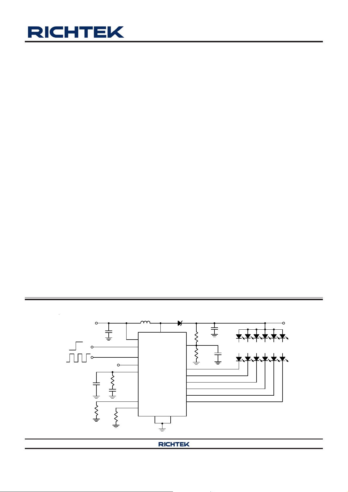
Simplified Application Circuit
V
IN
C
IN
Chip Enable
R
C
ISET
MIX
R
COMP
C
C
COMP
R
FSW
PWM Signal
L1
VIN
EN
PWM
MIX
COMP
ISET
FREQ
AGND
LX
RT8532
PGND
Applications
UMPC and Notebook Computer Backlight
D1
C
OUT
R
OVP
LED1
LED2
LED3
LED4
LED5
LED6
R
OVP2
OVP1
C
OVP
:
:
:
:
:
:
:
:
:
:
:
:
V
OUT
:
:
:
:
:
:
Copyright 2014 Richtek Technology Corporation. All rights reserved. is a registered trademark of Richtek Technology Corporation.
©
DS8532-04 January 2014 www.richtek.com
1
Page 2
RT8532
Ordering Information
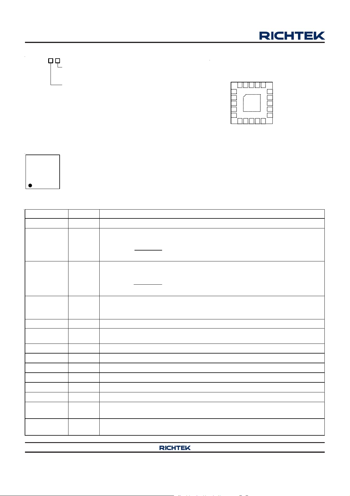
Pin Configurations
RT8532
Package Type
QW : WQFN-20L 3x3 (W-Type)
Lead Plating System
Note :
Richtek products are :
RoHS compliant and compatible with the current require-
ments of IPC/JEDEC J-STD-020.
Suitable for use in SnPb or Pb-free soldering processes.
G : Green (Halogen Free and Pb Free)
Marking Information
89= : Product Code
89=YM
YMDNN : Date Code
DNN
Functional Pin Description
Pin No. Pin Name Pin Function
1 EN Chip Enable (Active High). There is an internal pull low resistor 400k for the EN pin.
Switching Frequency of Boost Converter Setting. Connect a resistor between this pin
2 FREQ
3 ISET
4 MIX
5 AGND Analog Ground of LED Driver.
6, 7, 8, 9, 10,
11
LED6 to
LED1
12 OVP Over Voltage Protection Sense Input. The detecting threshold is 1.2V (typ.).
13, 14 PGND Power Ground of Boost Converter.
15, 16 LX Switching Pin of B oost Converter.
17 PWM PWM Dimming Control Input.
18 VDC Internal Regulator Voltage. Connect a capacitor from this pin to ground.
19 VIN Power Supply Input.
20 COMP
21
(Ex pos ed Pad)
GND
and AGND to set the switching frequency.
R1.1 6 k
FSW
25
F(MHz)
SW
LED C urre nt Set ting. LED cur rent is set by the re sisto r R
ISET pin to ground.
ImA
LED
240
Rk
ISET
Dimm in g Mod e Selec tio n. Th ere is an inte r na l pul l hi gh 4 00k resistor con nec t e d to
VDC. Floating or pulling high for 25% Mixed mode dimming, pulling low for direct
PWM mode dimming. Recommended to mixed mode for high LED efficiency.
Current Sink for LED String. (Leave the pin unconnected or short to GND, if not
used.)
Compensation Note for Boost Converter. Connect a compensation network to this pin
for stability.
Ground. The Exposed Pad must be Soldered to a Large PCB and Connected to GND
for Maximum Power Dissipation.
(TOP VIEW)
VIN
LED5
LX
PWM
VDC
16
17181920
15
LX
14
PGND
13
PGND
12
21
9876
LED4
OVP
115
10
LED3
LED2
con nected from the
ISET
COMP
1
EN
2
FREQ
3
ISET
MIX
AGND LED1
GND
4
LED6
WQFN-20L 3x3
Copyright 2014 Richtek Technology Corporation. All rights reserved. is a registered trademark of Richtek Technology Corporation.
www.richtek.com
2
©
DS8532-04 January 2014
Page 3
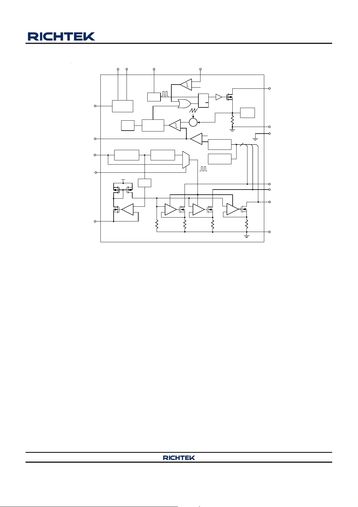
Function Block Diagram
VIN OVP
EN
COMP
PWM
MIX
LDO
PWM-to-DC
VDC
OTP
FREQ
OSC
PWM
Controller
Generator
PWMO
RT8532
+
1.2V
-
SQ
R
Q
OCP
+
+
-
0.6V
MUX
+
-
Mini LED
Selection
LED Open
Detection
6
LX
PGND
GND
DAC
+
-
ISET
+
-
Operation
Enable Control
When VIN is higher than the UVLO voltage and EN pin
input voltage is higher than rising threshold, the VDC will
be regulated around 3.8V if VIN is higher tha n 3.8V .
OSC
The switching frequency is adjustable by the external
resistor connected between the FREQ pin and GND.
PWM Controller
This controller includes some logic circuit to control LX
N-MOSFET on/off. This block controls the minimum on
time and max duty of LX.
LED1
LED2
……
LED6
AGND
+
-
……
+
-
MOSFET will be turned off until the temperature is lower
than the 120°C (typically).
OVP
When OVP pin voltage is higher than 1.2V, the LX
N-MOSFET is turned off immediately to protect the LX
N-MOSFET.
Minimum LED Selection
This block detects all LEDx voltage and select a minim um
voltage to EA (Error Amplifier). This function ca n guarantee
the lowest of LED pin voltage is around 600mV and V
OUT
can be boost to the highest forward voltage of LED strings.
OCP & OTP
When LX N-MOSFET peak current is higher than 2.5A
(typically), the LX N-MOSFET is turned off immediately
and resumed again at next clock pulse. When the junction
temperature is higher than 150°C (typically), the LX N-
Copyright 2014 Richtek Technology Corporation. All rights reserved. is a registered trademark of Richtek Technology Corporation.
DS8532-04 January 2014
©
LED Open Detection
If the voltage at LEDx pin is lower than 100mV, this
channel is defined a s open channel a nd the Minimum LED
Selection function will discard it to regulate other used
channels in proper voltage.
www.richtek.com
3
Page 4
RT8532
Absolute Maximum Ratings (Note 1)
Supply Input V oltage, VIN
EN, PWM, ISET, COMP , MIX, FREQ to GND ---------------------------------------------------------------------- −0.3V to 26.5V
LX, OVP , LED1 to LED6 to GN D--------------------------------------------------------------------------------------- −0.3V to 48V
LX t o G ND ------------------------------------------------------------------------------------------------------------------- −0.3V to 48V
to GND------------------------------------------------------------------------------------ −0.3V to 26.5V
< 500ns ---------------------------------------------------------------------------------------------------------------------- −1V to 48V
V DC to GND ---------------------------------------------------------------------------------------------------------------- −0.3V to 7V
Power Dissipation, P
@ T
D
= 25°C
A
WQFN−20L 3x3------------------------------------------------------------------------------------------------------------ 1.471W
Package Thermal Re sistance (Note 2)
WQFN−20L 3x3, θJA------------------------------------------------------------------------------------------------------ 68°C/W
WQFN−20L 3x3, θJC------------------------------------------------------------------------------------------------------ 7.5°C/W
Lead Temperature (Soldering, 10 sec.)------------------------------------------------------------------------------- 260°C
Junction T emperature----------------------------------------------------------------------------------------------------- 150°C
Storage T emperature Range -------------------------------------------------------------------------------------------- − 65°C to 150°C
ESD Susceptibility (Note 3)
HBM (Human Body Model)---------------------------------------------------------------------------------------------- 2kV
MM (Machine Model) ----------------------------------------------------------------------------------------------------- 200V
Recommended Operating Conditions (Note 4)
Supply Input Voltage, VIN ----------------------------------------------------------------------------------------------- 2.5V to 24V
Junction T emperature Range-------------------------------------------------------------------------------------------- −40°C to 125°C
Ambient T emperature Range-------------------------------------------------------------------------------------------- −40°C to 85°C
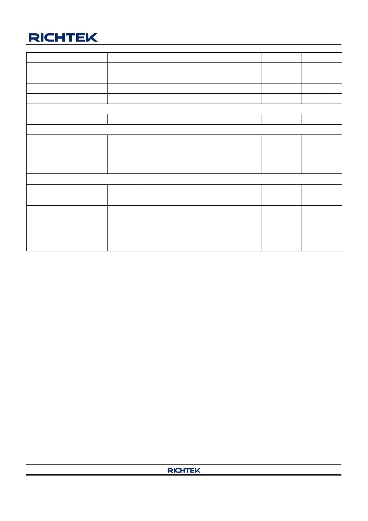
Electrical Characteristics
(V
= 5V, TA = 25°C, unless otherwise specified)
IN
Parameter Symbol Test Conditions Min Typ Max Unit
I
VIN Quiescent Current
VIN Shutdown Current I
VI N Unde r Vol tage Lock ou t
Threshold
PWM Dimm ing Frequency f
VIN
I
VIN_SW
SHDN
V
PWM
Control Input
EN, PWM Inp ut
Voltage
High V
Low VIL
Boost Converter
Switching Frequency fSW
LX On Resista nc e
(N-MOSFET)
R
UVLO
0.1 -- 20 kHz
IH
V
LX
PWM = COMP = 0V, Not Switching
-- 3 --
PWM = COMP = 2V, Sw itching -- 4 --
-- -- 10 A
-- 2.1 --
1.3 -- 24
-- -- 0.5
0.8 1 1.2
0.4 0.5 0.6
= 4.5V, EN = 0V
V
IN
V
Rising -- 2.3 --
IN
VIN Falling
= 2.5V to 24V
V
IN
= 2.5V to 24V
V
IN
R
= 22k
FSW
R
= 51k
FSW
> 4.5V 0 .18 0.2 0 .22
IN
mA
V
V
MHz
Copyright 2014 Richtek Technology Corporation. All rights reserved. is a registered trademark of Richtek Technology Corporation.
www.richtek.com
4
©
DS8532-04 January 2014
Page 5
RT8532
A
A
Parameter Symbol Test Conditions Min Typ Max Unit
Minimum On-Time t
ON(MIN)
Maximum Duty D
LX Cur rent Limi t I
Regulat ed V
V
LEDx
LIM
Low Dropout Linear Regulator
LDO O utput Vol tag e Ra nge VDC 3.6 3.8 4 V
LED Current Pr ogramming
LED Current Accuracy I
LE D Curr en t Matc hi ng I
LEDA
LEDM
ISET Pin Voltage V
F ault Protecti on
FSW = 1MHz 40 60 80 n s
FSW = 1MHz 90 93 96 %
MAX
LEDx
ISET
Hi gh est LE D Strin g, I
2V > V
2V > V
Formulated by (I
LEDx
LEDx
> 0.5V, R
> 0.5V, R
LEDx
LED
ISET
ISET
I
= 20mA
= 12k
= 12k,
) / I
VG
x 100%
VG
2.2 2.5 2.8 A
0.5 0.6 0.7 V
19.4 20 20.6 mA
-- -- 2 %
0.76 1 1.24 V
OVP Threshol d V
OVP UVLO Threshold V
T herm al Shutdow n
Temperature
OTP H ysteresis T
LE D Pi n Unde r Vol tag e
Threshold
Note 1. Stresses beyond those listed “Absolute Maximum Ratings” may cause permanent damage to the device. These are
stress ratings only, and functional operation of the device at these or any other conditions beyond those indicated in
the operational sections of the specifications is not implied. Exposure to absolute maximum rating conditions may
affect device reliability.
Note 2. θ
Note 3. Devices are ESD sensitive. Handling precaution is recommended.
Note 4. The device is not guaranteed to function outside its operating conditions.
is measured at T
JA
measured at the exposed pad of the package.
= 25°C on a high effective thermal conductivity four-layer test board per JEDEC 51-7. θJC is
A
1.16 1.2 1.24 V
OVP
OVPF
T
-- 150 -- C
SD
OTP_Hys
V
LSD
-- 30 -- C
Un-Connection -- 0.1 -- V
-- 50 -- mV
Copyright 2014 Richtek Technology Corporation. All rights reserved. is a registered trademark of Richtek Technology Corporation.
DS8532-04 January 2014
©
www.richtek.com
5
Page 6

RT8532
Typical Application Circuit
V
5V to 24V
Chip Enable
PWM Signal
L1
R1
10
C1
100nF
COMP
COMP
R
FSW
51k
10µH
19
1
17
20
3
2
VIN
EN
PWM
COMP
ISET
FREQ
AGND
LX
RT8532
PGND
IN
C
IN
4.7µF
R
5.1k
C
22nF
R
ISET
12k
5
15, 16
13, 14
D1
SS16
R
500k
12
OVP
R
15k
4
MIX
18
VDC
11
LED1
10
LED2
9
LED3
8
LED4
7
LED5
6
LED6
GND
21 (Exposed Pad)
OVP2
OVP1
C
0.1µF
DC
C
OUT
4.7µF
C
OVP
47pF
V
OUT
43V MAX
:
:
:
:
:
:
:
:
:
:
:
:
:
:
:
:
:
:
Figure 1. For General Application Circuit
V
2.5V to 24V
IN
5V
Chip Enable
PWM Signal
R1
10
R
12k
ISET
R
COMP
5.1k
C
22nF
R
51k
C
IN
4.7µF
C1
100nF
COMP
FSW
10µH
19
1
17
20
3
2
L1
VIN
EN
PWM
COMP
ISET
FREQ
AGND
LX
RT8532
PGND
5
15, 16
13, 14
D1
SS16
OVP
VDC
LED1
LED2
LED3
LED4
LED5
LED6
GND
R
OVP2
500k
12
R
OVP1
24k
4
MIX
18
C
0.1µF
11
10
9
8
7
6
21 (Exposed Pad)
DC
C
OUT
4.7µF
C
47pF
Figure 2. For Low Input Voltage Application Circuit
OVP
V
OUT
25V MAX
depends
(V
OUT
on D
:
:
:
:
:
:
:
:
:
:
:
:
:
:
:
:
:
:
MAX
)
Copyright 2014 Richtek Technology Corporation. All rights reserved. is a registered trademark of Richtek Technology Corporation.
www.richtek.com
©
DS8532-04 January 2014
6
Page 7

Typical Operating Characteristics
)
)
RT8532
Efficiency vs. Input Voltage
100
90
80
70
60
50
40
Efficiency (%)
30
20
10
0
4 8 12 16 20 24
54 LEDs, fSW = 500kHz, PWM = 3.3V
Inpu t Volta ge (V)
LED Curre nt vs. Temperature
26
24
22
LED Curre nt vs. Input Voltage
26
LED1
24
22
20
18
LED2
LED3
LED4
LED5
LED6
Output Current (mA
16
14
9 LEDs per channel, fSW = 500kHz, PWM = 3.3V
4 8 12 16 20 24
Input Voltage (V)
VDC vs. Temperature
5.0
4.5
4.0
(kHz)
SW
f
20
18
LED Current (mA)
16
14
9 LEDs per channel, fSW = 500kHz, PWM = 3.3V
-50 -25 0 25 50 75 100 125
Tempera ture (°C)
fSW vs. R
2000
1800
1600
1400
1200
1000
800
600
400
200
0 20 40 60 80 100 120 140
R
FSW
FSW
9 LEDs per channel
(kohm)
(kΩ)
3.5
VDC (V)
3.0
2.5
2.0
-50 -25 0 25 50 75 100 125
9 LEDs per channel, fSW = 500kHz
Temperature (°C)
LED Current v s. PWM Duty Cycle
20
16
12
8
LED Current (mA
4
0
0 20406080100
9 LEDs per channel, fSW = 500kHz
PWM 100Hz
PWM 1kHz
PWM 10kHz
PWM 20kHz
PW M Duty Cycle (%)
Copyright 2014 Richtek Technology Corporation. All rights reserved. is a registered trademark of Richtek Technology Corporation.
DS8532-04 January 2014
©
www.richtek.com
7
Page 8

RT8532
)
1.4
1.3
1.2
1.1
OVP Threshold Voltage (V)
1.0
V
IN
(10V/Div)
OVP Threshold Voltage vs. Input Voltage
9 LEDs per channel, fSW = 500kHz
4 8 12 16 20 24
Inp ut Volta g e (V)
Line Transient Response
2.5
2.3
2.0
1.8
Quiescent Current (mA
1.5
V
IN
(10V/Div)
V
EN
(5V/Div)
V
PWM
(5V/Div)
Qu iescent Curren t vs. Input Voltage
Not Switching
3 5 8 10131518202325
Inp ut Volta g e (V)
Power On in PWM Mode
I
LED
(20mA/Div)
V
OUT
(20V/Div)
V
EN
(5V/Div)
V
LX
(20V/Div)
I
LED
(20mA/Div)
VIN = 12V to 18V, fSW = 500kHz, PWM = 3.3V
Time (2.5ms/Div)
Power On from EN
VIN = 12V, fSW = 500kHz, PWM = 3.3V
Time (10ms/Div)
I
LED
(20mA/Div)
V
IN
(20V/Div)
V
PWM
(5V/Div)
V
EN
(5V/Div)
I
LED
(20mA/Div)
VIN = 12V, fSW = 500kHz
Time (10ms/Div)
Power On in Mixed Mode
VIN = 12V, fSW = 500kHz
Time (10ms/Div)
Copyright 2014 Richtek Technology Corporation. All rights reserved. is a registered trademark of Richtek Technology Corporation.
www.richtek.com
©
DS8532-04 January 2014
8
Page 9

Application Information
RT8532
The RT8532 is a general purpose 6-CH LED driver ca pable
of delivering an adjustable 5mA to 50mA LED current. The
IC is a current mode boost converter integrated with a
43V/2.5A power switch and can cover a wide VIN ra nge
from 2.5V to 24V. The part integrates both built-in softstart and with PWM dimming control; moreover , it provides
over voltage, over temperature and current limiting
protection features. It also integrates PWM and mixed
mode dimming function for a ccurate LED current control.
The PWM dimming frequency can operate from 100Hz to
20kHz without inducing any inrush current in LED or
inductor.
Input Capacitor Selection
Low ESR ceramic ca pa citors are recommended for input
capacitor applications. Low ESR will effectively reduce
the input ripple voltage caused by the switching operation.
Two 2.2μF low ESR ceramic capa citors are suff icient f or
most applications. Nevertheless, this value can be
decreased for applications with lower output current
requirement. Another consideration is the voltage rating
of the input capacitor, which must be greater than the
maximum input voltage.
where fSW is the switching frequency and ΔIL is the inductor
ripple current. Move C
value of ΔV
V
OUT1
according to the following equation :
OUT1
DI
OUT
Cf
OUT SW
to the left side to estimate the
OUT
Finally, taking ESR into a ccount, the overall output ripple
voltage can be determined by the following equation :
DI
VIESR
OUT IN
Input Current
ΔV
OUT1
OUT
Cf
OUT SW
Inductor Current
Output Current
(1-D)T
S
ΔI
L
Output Ripple
Voltage (ac)
Time
Time
Output Capacitor Selection
Output ripple voltage is an i mportant index f or estimating
chip performa nce. This portion consists of two parts. One
is the product of the inductor current ripple with the ESR
of the output cap acitor, while the other part is formed by
the charging and discharging process of the output
ca pacitor . As shown in Figure 3, ΔV
can be evaluated
OUT1
ba sed on the ideal energy equalization. According to the
definition of Q, the Q value can be calculated as the
following equation :
11 1
QIIIIII
C V
IN L OUT IN L OUT
22 2
V
Vf
OUT SW
IN
1
OUT OUT1
Figure 3. The Output Ripple Voltage without the
Contribution of ESR
Inductor Selection
The inductor value depends on the maximum input current.
As a general rule the inductor ripple current is 20% to
40% of maximum input current. If 40% is selected as an
example, the inductor ripple current can be calculated
according to the f ollowing equation :
VI
OUT OUT(MAX)
I
IN(MAX)
I0.4I
RIPPLE IN(MAX)
V
IN
Copyright 2014 Richtek Technology Corporation. All rights reserved. is a registered trademark of Richtek Technology Corporation.
DS8532-04 January 2014
©
www.richtek.com
9
Page 10

RT8532
where η is the ef ficiency of the boost converter , I
the maximum input current and I
is the inductor ripple
RIPPLE
IN(MAX)
is
current. The input pea k current can be obtained by adding
the maximum input current with half of the inductor ripple
current as shown in the f ollowing equation :
I
= 1.2 x I
PEAK
IN(MAX)
Note that the saturated current of inductor must be greater
than I
. The inductance ca n eventually be determined
PEAK
according to the following equation :
2
VDV V
L1
where V
IN OUT IN
0.4 V I f
is the maximum output voltage, VIN is the
OUT
2
OUT OUT SW
minimum input voltage, fSW is the switching frequency,
and I
is the sum of current from all LED strings.
OUT
LED Soft-Start Function
The soft-start time of the LED boost converter, defined a s
the period from EN to set I
, is several tens of
OUT
milliseconds according to the difference of PWM or Mixed
mode. The LED starts up after VIN, PWM and EN signals
are all ready. The soft-start inrush peak current must be
less than 2.5A.
LED Driver Compensation
The control loop can be compensated by adjusting the
external components connected to the COMP pin. The
COMP pin is the output of the internal error a mplifier. The
compensation capacitors, CC and C
, will adjust the
COMP
integrator zero and pole respectively to maintain stability .
Moreover, the resistor, R
, will adjust the mid-band
COMP
gain for fa st tran sient response.
Diode Selection
Setting and Regulation of LED Current
The LED current can be calculated by the following
equation :
ImA
LED
where R
ISET
240
Rk
ISET
is the resistor between the ISET pin and GND.
This setting is the reference for the LED current at LED1
to LED6 and represents the sensed LED current for ea ch
string. The DC/DC converter regulates the LED current
according to the setting.
PWM Mode and Mixed Mode Brightness Dimming
The RT8532 allows two ways of controlling the LED
brightness.
PWM Mode Di mming : When the MIX pin is connected to
GND, the dimming mode operates in PWM Mode. During
the PWM dimming, the current source turn-on/off is
synchronized with the PWM signal. The LED current
frequency is equivalent to PWM input frequency .
Mixed Mode Di mming : If the MIX pin is floating or tied to
V DC, the dimming mode operates in Mixed Mode. In this
mode the PWM and I
dimming cycle will delay by 2
LED
periods. First cycle delay is required for the period, while
the second cycle delay is for the duty rate calculation.
(a) When 25% ≤ PWM duty ≤ 100%, the current source
outputs are DC dimming, and the PWM duty cycle
modulates the amplitude of the currents.
(b) When PWM Duty < 25%, the DC dimming will tra nslate
to DC-PWM dimming to control the LED current. In this
state, the LED current is fixed at 0.25 x ISET, and the
dimming duty is 4 x PWM duties. The minimum D/A
Converter is 512 steps resolution for I
regulation.
LED
Schottky diodes D1 are recommended for most
applications because of their fast recovery time and low
forward voltage. Power dissipation, reverse voltage rating,
and pulsating pea k current are i mportant parameters for
consideration when making a Schottky diode selection.
Make sure that the diode's peak current rating exceeds
I
and reverse voltage rating exceeds the maximum
PEAK
output voltage.
Copyright 2014 Richtek Technology Corporation. All rights reserved. is a registered trademark of Richtek Technology Corporation.
www.richtek.com
10
©
DS8532-04 January 2014
Page 11

RT8532
Brightness Control
The RT8532 features the digital dimming control scheme.
A very high contrast ratio true digital PWM dimming can
be achieved by driving PWM pin with a PWM signal a nd
the recommended PWM frequency is 100Hz to 10kHz.
Dimming frequency can be sufficiently adjusted from
100Hz to 20kHz. However, LED current cannot be 100%
proportional to duty cycle especially for high frequency
and low duty ratio because of physical li mitation caused
by inductor rising time. Plea se refer to T a ble 1 and Table2.
Table 1. Mixed Dimming Mode
Dimming Frequency (Hz) Duty (Min) Duty (Max)
100 < f
200 < f
500 < f
1k < f
2k < f
5k < f
10k < f
200 0.18% 100%
PWM
500 0.18% 100%
PWM
1k 0.2% 100%
PWM
2k 0.2% 100%
PWM
5k 0.3% 100%
PWM
10k 0.3% 100%
PWM
20k 0.6% 100%
PWM
Table 2. PWM Dimming Mode
Dimming Frequency (Hz) Duty (Min) Duty (Max)
100 < f
200 < f
500 < f
1k < f
2k < f
5k < f
10k < f
Note : The minimum duty in T able 1 and Table 2 is based
on the application circuit and does not consider the
deviation of current linearity when f
may not achieve setting current in duty (min.) due to
different VOUT / VIN ratio at VIN = 12V .
200 0.02% 100%
PWM
500 0.02% 100%
PWM
1k 0.04% 100%
PWM
2k 0.06% 100%
PWM
5k 0.15% 100%
PWM
10k 0.3% 100%
PWM
20k 0.6% 100%
PWM
> 10kHz, ILED
PWM
Over Temperature Protection
The RT8532 includes an Over Temperature Protection
(OTP) feature to prevent overheating due to excessive
power dissipation from damaging the device. The OTP
function will shut down LED driver when the junction
temperature exceeds 150°C. It will reactivate the device
when powered on again. T o maintain continuous operation,
the junction temperature should be kept below 125°C.
LED Driver Over Voltage Protection
The LED driver equi ps an Over Voltage Protection (OVP)
function. When the voltage at the OVP pin reaches a
threshold of approximately 1.2V, the driver will turn off.
The drivers turn on again once the voltage at OVP drops
below the threshold voltage. Thus, the output voltage can
be clamped at a certain voltage level. This voltage level
can be calculated by the following equation :
R
VV1
OUT, OVP OVP
where R
and R
OVP1
OVP2
R
OVP1
are the resistors in the voltage
OVP2
divider connected to the OVP pin. It is suggested to use
500kΩ for R
to reduce loading effect.
OVP2
LED Channel Open Circuit Protection
If at least one channel is in normal operation, the LED
driver will automatically ignore the open channels and
continue to regulate current for the channels in normal
operation.
Under Voltage Lockout (UVLO)
The UVLO circuit compares the LED driver input voltage
at VIN with the UVLO threshold to ensure the input voltage
is high enough for reliable operation. The 200mV (typ.)
hysteresis prevents supply transients from causing a
shutdown. Once VIN exceeds the UVLO rising threshold,
the LED soft-start will begin after a several ms delay . When
VIN falls below the UVLO falling threshold, the controller
turns off all LED driver functions.
Copyright 2014 Richtek Technology Corporation. All rights reserved. is a registered trademark of Richtek Technology Corporation.
DS8532-04 January 2014
©
www.richtek.com
11
Page 12

RT8532
Thermal Considerations
For continuous operation, do not exceed absolute
maximum junction temperature. The maximum power
dissipation depends on the thermal resistance of the IC
package, PCB layout, rate of surrounding airflow, and
difference between junction and a mbient temperature. The
maximum power dissipation can be calculated by the
following formula :
P
where T
the ambient temperature, a nd θ
D(MAX)
= (T
J(MAX)
− TA) / θ
J(MAX)
JA
is the maximum junction temperature, TA is
is the junction to ambient
JA
thermal resistance.
For recommended operating condition specifications, the
maximum junction temperature is 125°C. The junction to
ambient thermal resista nce, θJA, is layout dependent. For
WQF N-20L 3x3 pa ckages, the thermal resista nce, θJA, is
68°C/W on a standard JEDEC 51-7 f our-layer thermal test
board. The maximum power dissipation at TA = 25°C can
be calculated by the following formula :
Layout Considerations
PCB layout is very important to design power switching
converter circuits. The following layout guide lines should
be strictly followed for best performa nce of the RT8532.
The power components L1, D1, C
and C
IN
must be
OUT
placed as close as possible to reduce the ac current
loop. The PCB trace between power components must
be short and wide a s possible due to large current flow
through these trace during operation.
Place L1 and D1 as close to LX pins as possible. The
trace should be short a nd wide as possible.
Place the input capacitor C1 close to VIN pin.
Pin 20 is the compensation point to adjust system
stability. Place the compensation components to pin
20 as close as possible.
P
= (125°C − 25°C) / (68°C/W) = 1.471W for
D(MAX)
WQF N-20L 3x3 pa ckage
The maximum power dissipation depends on the operating
ambient temperature for fixed T
and thermal
J(MAX)
resistance, θJA. The derating curve in Figure 4 allows the
designer to see the effect of rising ambient temperature
on the maximum power dissipation.
1.6
1.4
1.2
1.0
0.8
0.6
0.4
0.2
Maximum Pow er Dissipat ion (W) 1
0.0
0 255075100125
Ambient Temperatur e (°C)
Four-Layer PCB
Figure 4. Derating Curve of Maxi mum Power Dissi pation
Copyright 2014 Richtek Technology Corporation. All rights reserved. is a registered trademark of Richtek Technology Corporation.
www.richtek.com
12
©
DS8532-04 January 2014
Page 13

Locate the C1
as close to VIN
as possible.
The compensation circuit should be
kept away from the power loops and
should be shielded with a ground
trace to prevent any noise coupling.
C
COMP
R
COMP
GND
Place the power components as
close as possible. The traces should
be wide and short especially for the
high-current loop.
L1
R1
C1
V
C
D1
IN
IN
GND
VOUT
RT8532
C
OUT
Locate the R
to ISET as possible.
GND
ISET
R
as close
ISET
20
VIN
COMP
EN
1
2
FREQ
3
4
5
ISET
MIX
AGND
LED6
GND
LED5
Figure 5. PCB Layout Guide
17
1819
VDC
LED4
897610
PWM
LED3
16
LX
LED2
LX
PGND
PGND
OVP
LED1
15
14
13
12
11
GND
Copyright 2014 Richtek Technology Corporation. All rights reserved. is a registered trademark of Richtek Technology Corporation.
DS8532-04 January 2014
©
www.richtek.com
13
Page 14

RT8532
Outline Dimension
1
2
DETAIL A
Pin #1 ID a nd T ie Bar Mark Option s
Note : The configuration of the Pin #1 identifier is optional,
but must be located within the zone indicated.
Dimensions In Millimeters Dimensio ns In Inches
Symbol
Min Max Min Max
A 0.700 0.800 0.028 0.031
A1 0.000 0.050 0.000 0.002
A3 0.175 0.250 0.007 0.010
b 0.150 0.250 0.006 0.010
D 2.900 3.100 0.114 0.122
D2 1.650 1.750 0.065 0.069
E 2.900 3.100 0.114 0.122
1
2
E2 1.650 1.750 0.065 0.069
e 0.400 0.016
L 0.350 0.450
0.014 0.018
W-Type 20L QFN 3x3 Package
Richtek Technology Corporation
14F, No. 8, Tai Yuen 1st Street, Chupei City
Hsinchu, Taiwan, R.O.C.
Tel: (8863)5526789
Richtek products are sold by description only. Richtek reserves the right to change the circuitry and/or specifications without notice at any time. Customers should
obtain the latest relevant information and data sheets before placing orders and should verify that such information is current and complete. Richtek cannot
assume responsibility for use of any circuitry other than circuitry entirely embodied in a Richtek product. Information furnished by Richtek is believed to be
accurate and reliable. However, no responsibility is assumed by Richtek or its subsidiaries for its use; nor for any infringements of patents or other rights of third
parties which may result from its use. No license is granted by implication or otherwise under any patent or patent rights of Richtek or its subsidiaries.
www.richtek.com
14
DS8532-04 January 2014
Page 15

 Loading...