

®
43V Asynchronous Boost WLED Driver
RT8511B
General Description
The RT851 1B is an LED driver IC that can support up to
10 WLED in series. It is composed of a current mode
boost converter integrated with a 43V/2.2A power switch
running at a fixed 500kHz frequency and covering a wide
VIN ra nge from 2.7V to 24V.
The white LED current is set with a n external resistor , and
the feedback voltage is regulated to 200mV (typ.). During
operation, the LED current ca n be controlled by the PWM
input signal in which the duty cycle determines the
feedback reference voltage.
For brightness dimming, the RT851 1B is able to maintain
steady control of the LED current. Therefore, no audible
noises are generated on the output cap acitor . The RT851 1B
also has programmable over voltage pin to prevent the
output from exceeding absolute maximum ratings during
open LED conditions. The RT8511B is available in
W DF N-8L 2x2 package.
Features
Wide Input Voltage Range : 2.7V to 24V
High Output Voltage : up to 43V
Direct PWM Dimming Control and Frequency from
100Hz to 8kHz
Internal Soft-Start and Compensation
200mV Reference Voltage
PWM Dimming with Internal Filter
Programmable Over Voltage Protection
Over Temperature Protection
Current Limit Protection
Thin 8-Lead WDFN Package
RoHS Compliant and Halogen Free
Applications
UMPC and Notebook Computer Backlight
GPS, Portable DVD Backlight
Ordering Information
RT8511B
Package Type
QW : WDFN-8L 2x2 (W-Type)
Lead Plating System
G : Green (Halogen Free and Pb Free)
Note :
Richtek products are :
RoHS compliant and compatible with the current require-
ments of IPC/JEDEC J-STD-020.
Suitable for use in SnPb or Pb-free soldering processes.
Pin Configurations
(TOP VIEW)
1
OVP
2
FB
3
DIMC
GND
WDFN-8L 2x2
GND
4
9
Marking Information
0F : Product Code
0FW
W : Date Code
8
7
6
5
EN
PWM
VIN
LX
Copyright 2015 Richtek Technology Corporation. All rights reserved. is a registered trademark of Richtek Technology Corporation.
©
DS8511B-05 February 2015 www.richtek.com
1
RT8511B
Typical Application Circuit
V
4.2V to 24V
Chip Enable
100Hz to 8kHz
V
2.7V to 24V
Chip Enable
100Hz to 8kHz
IN
PWM
LED
2.7V to 4.2V
PWM
C
IN
1µF x 2
C
DIMC
1µF
Figure 1. T ypical Application Circuit of Normal Operation
C
LED
1µF x 2
V
IN
C
DIMC
1µF
C
1µF
IN
6
8
7
3
6
8
7
3
VIN
EN
PWM
DIMC
VIN
EN
PWM
DIMC
L
10µH
RT8511B
L
10µH
RT8511B
5
LX
1
OVP
2
FB
4, 9 (Exposed Pad)
GND
5
LX
1
OVP
2
FB
4, 9 (Exposed Pad)
GND
V
D
R2
3.3M
C
OUT
1µF x 2
R1
100k
D
R2
3.3M
C
OUT
1µF x 2
R1
100k
:
:
:
:
OUT
:
:
:
:
WLEDs
:
:
:
:
R
SET
3.3
V
OUT
:
:
:
:
:
:
:
:
WLEDs
:
:
:
:
R
SET
3.3
Figure 2. T ypical Application Circuit of Low V oltage Operation
Functional Pin Description
Pin No. Pin Name Pin Function
1 OVP Over Voltage Protection for Boost Converter. The detecting threshold is 1.2V.
2 FB Feedback. Connect a resistor between this pin and GND to set the LED current.
3 DIMC PW M Fil t er. Filter the PW M sig nal to a DC vol t ag e.
4 GND Ground.
5 LX Switch Node for Boost Converter.
6 VIN Power Supply Input.
7 PWM Dimming Control Input.
8 EN Chip Enable (Active High) for Boost Converter.
9 (Exp ose d Pa d) GN D
Copyright 2015 Richtek Technology Corporation. All rights reserved. is a registered trademark of Richtek Technology Corporation.
2
©
The exposed pad must be soldered to a large PCB and connected to AGND for
ma x imum power dissipation.
DS8511B-05 February 2015www.richtek.com
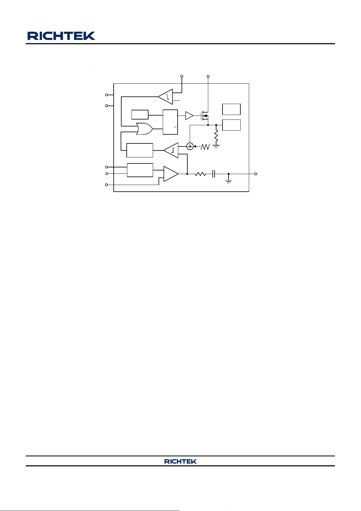
Function Block Diagram
RT8511B
LXOVP
VIN
EN
PWM
DIMC
FB
OSC
PWM
Controller
D/A
Dimming
+
1.2V
-
QS
R
Q
+
+
-
OTP
OCP
GND
Copyright 2015 Richtek Technology Corporation. All rights reserved. is a registered trademark of Richtek Technology Corporation.
©
DS8511B-05 February 2015 www.richtek.com
3
RT8511B
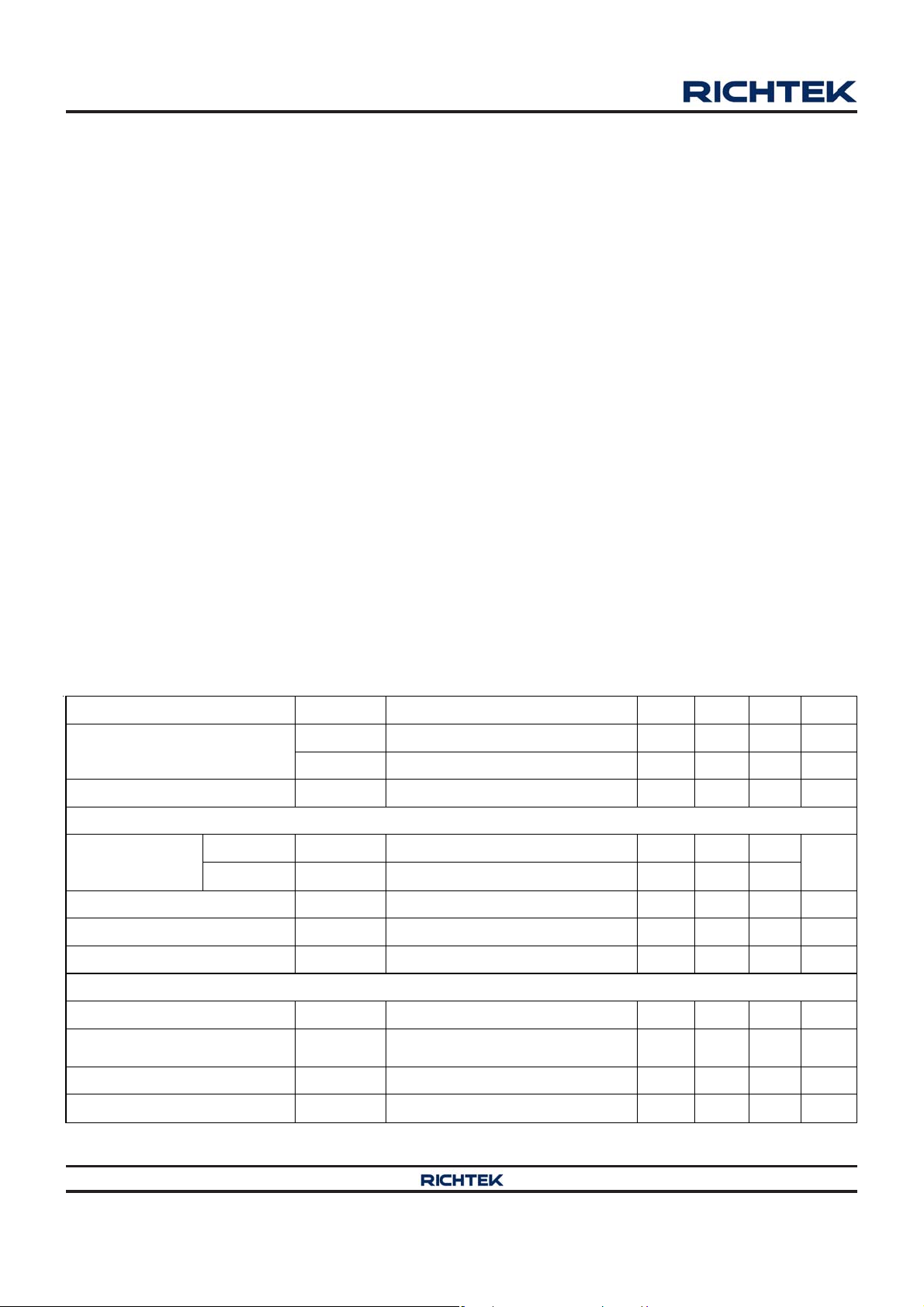
Absolute Maximum Ratings (Note 1)
VIN, EN, PWM, DIMC to GND------------------------------------------------------------------------------------------ −0.3V to 26.5V
FB, OVP to GND ---------------------------------------------------------------------------------------------------------- −0.3V to 48V
LX to GND ------------------------------------------------------------------------------------------------------------------ −0.3V to 48V
< 500ns ---------------------------------------------------------------------------------------------------------------------- −1V to 48V
Power Dissipation, P
WDFN-8L 2x2 -------------------------------------------------------------------------------------------------------------- 0.833W
Package Thermal Re sistance (Note 2)
W DF N-8L 2x2, θJA--------------------------------------------------------------------------------------------------------- 120°C/W
WDFN-8L 2x2, θJC--------------------------------------------------------------------------------------------------------- 8.2°C/W
Lead Temperature (Soldering, 10 sec.)------------------------------------------------------------------------------- 260°C
Junction T emperature----------------------------------------------------------------------------------------------------- 150°C
Storage T emperature Range -------------------------------------------------------------------------------------------- –65°C to 150°C
ESD Susceptibility (Note 3)
HBM (Human Body Model)---------------------------------------------------------------------------------------------- 2kV
MM (Machine Model) ----------------------------------------------------------------------------------------------------- 200V
@ TA = 25°C
D
Recommended Operating Conditions
Supply Input V oltage, V
Junction T emperature Range-------------------------------------------------------------------------------------------- −40°C to 125°C
Ambient T emperature Range-------------------------------------------------------------------------------------------- −40°C to 85°C
------------------------------------------------------------------------------------------------ 2.7V to 24V
IN
(Note 4)
Electrical Characteristics
(V
= 4.5V, T
IN
VIN Quiescent Current
VIN Shutdown Current I
Control In put
EN, PWM
Threshold Voltage
EN Sink Current IIH V
Shutdown Delay t
PWM Dimming Frequenc y 0.1 - - 8 kHz
Boost Converter
= 25°C, unless otherwise specified)
A
Parameter Symbol Test Conditions Min Typ Max Unit
Logic-High V
V
I
Q
I
VFB = 0V, Switching -- -- 2.2 mA
Q_SW
V
SHDN
V
IH
= 1.5V, No Switching -- 725 -- A
FB
= 4.5V, VEN = 0V -- 1 4 A
IN
= 2.7V to 24V 1.6 -- --
IN
V
Logic-Low VIL V
EN high to low 52 64 80 ms
SHDN
= 2.7V to 24V -- -- 0.8
IN
= 3V 1 -- 10 A
EN
Switching Frequency f
LX On Resistance
(N-MOSFET)
V
OSC
R
VIN > 5V -- 0.4 0.6
DS(ON)
= 2.7V to 24V 0.4 0.5 0.6 MHz
IN
Minimum ON T i me -- 6 0 -- ns
Maximum Duty Cycle D
Copyright 2015 Richtek Technology Corporation. All rights reserved. is a registered trademark of Richtek Technology Corporation.
4
©
V
MAX
= 0V, Switching -- 92 -- %
FB
DS8511B-05 February 2015www.richtek.com

RT8511B
Parameter Symbol Test Conditions Min Typ Max Unit
LED Current
Minimum PWM Dimming Duty
Cycle
Feedback Voltage VFB 195 200 205 mV
Fault Protection
Dimming Freq. = 100Hz to 8kHz 1 -- -- %
D
MIN
LX Current Limit I
Over Voltage Protection
Threshold
Thermal Shutdown
Temperature
1.66 2.2 2.74 A
LIM
1.14 1.2 1.26 V
V
OVP
-- 160 -- °C
T
SD
Thermal Shutdown Hysteresis TSD -- 30 -- °C
Note 1. Stresses beyond those listed “Absolute Maximum Ratings” may cause permanent damage to the device. These are
stress ratings only, and functional operation of the device at these or any other conditions beyond those indicated in
the operational sections of the specifications is not implied. Exposure to absolute maximum rating conditions may
affect device reliability.
Note 2. θ
Note 3. Devices are ESD sensitive. Handling precaution is recommended.
Note 4. The device is not guaranteed to function outside its operating conditions.
is measured at T
JA
measured at the exposed pad of the package.
= 25°C on a high effective thermal conductivity four-layer test board per JEDEC 51-7. θJC is
A
Copyright 2015 Richtek Technology Corporation. All rights reserved. is a registered trademark of Richtek Technology Corporation.
DS8511B-05 February 2015 www.richtek.com
©
5
RT8511B
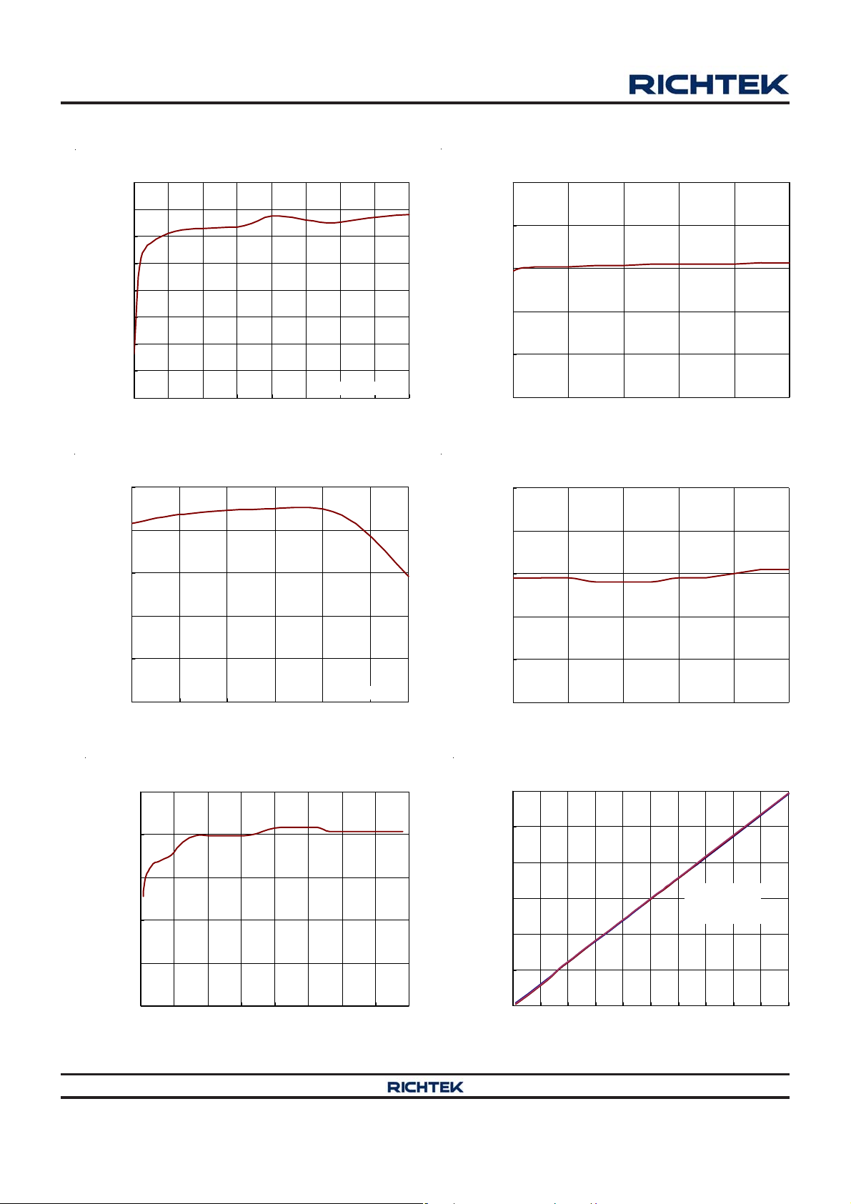
Typical Operating Characteristics
Efficiency vs. Input Voltage
100
95
90
85
80
75
Efficiency (%)
70
65
V
60
4 7 9 121417192224
OUT
Inp ut Vol tage (V)
FB Reference Voltage vs. Te m perature
200
198
196
= 29.5V
FB Reference Voltage vs. Input Voltage
199.5
199.2
198.9
198.6
198.3
FB Refer ence V oltage ( m V)
198.0
4 8 12 16 20 24
Input Vol tage (V)
Frequency vs. Input Voltage
600
550
500
194
192
FB Reference Voltage (mV)
190
-20 5 30 55 80 105
Temperature (°C)
Current Lim it vs. Input Voltage
3.0
2.6
2.2
1.8
Current Lim it ( A)
1.4
1.0
2.5 5.25 8 10.75 13.5 16.25 19 21.75 24.5
Inpu t Voltage (V)
V
IN
= 4.5V
450
Frequency ( kH z) 1
400
350
4 8 12 16 20 24
Input Vol tage (V)
LED Current vs. PWM Duty Cycle
60
50
40
30
20
LED Current (mA)
10
0
0 102030405060708090100
PWM Duty Cycle (%)
PWM = 100Hz
= 2kHz
PWM
PWM = 8kHz
Copyright 2015 Richtek Technology Corporation. All rights reserved. is a registered trademark of Richtek Technology Corporation.
©
DS8511B-05 February 2015www.richtek.com
6

Application Information
RT8511B
The RT8511B is a current mode boost converter which
operates at a fixed frequency of 500kHz. It is ca pa ble of
driving up to 10 white LEDs in series and integrates
functions such as soft-start, compensation, and internal
analog di mming control. The protection block also provides
over-voltage, over-temperature, and current- limit protection
features.
LED Current Setting
The loop structure of the boost converter keeps the FB
pin voltage equal to the reference voltage VFB. Therefore,
by connecting the resistor, R
between the FB pin and
SET
GND, the LED current will be determined by the current
through R
. The LED current can be calculated by the
SET
following equation :
V
I =
LED
R
FB
SET
Brightness Control
For the brightness dimming control of the RT8511B, the
IC provides typically 200mV reference voltage when the
PWM pin is constantly pulled high. However, the PWM
pin allows a PWM signal to adjust the reference voltage
by changing the PWM duty cycle to achieve LED
brightness dimming control. The relationship between the
duty cycle and the FB voltage can be calculated a ccording
to the following equation :
VFB = 200mV x Duty
where 200mV is the typical internal reference voltage and
Duty is the duty cycle of the PWM signal.
As shown in Figure 3, the duty cycle of the PWM signal
is used to modify the internal 200mV reference voltage.
With an on-chip output clamping amplifier and a serial
resistor, the PWM dimming signal is easily low-pass
filtered to an analog dimming signal with one external
cap a citor, C
, for noise-free PWM dimming. Di mming
DIMC
frequency can be sufficiently a djusted from 100Hz to 8kHz.
However, the LED current cannot be 100% proportion al to
the duty cycle. Referring to T a ble 1, the minimum dimming
duty can be as low as 1% for the frequency range from
100Hz to 8kHz. It should be noted that the accuracy of
1% duty is not guaranteed.
Because the voltage of DIMC a nd FB is small to 2mV a nd
ea sily affected by LX switching noise.
200mV
DIMC
PWM
R
C
DIMC
1µF
FB
+
EA
-
To
Controller
Figure 3. Block Di agra m of Progra mma ble FB Voltage
Table 1. Minimum Duty for Dimming Frequency
Dimming Frequency Minimum Duty Cycle
100Hz to 8kHz 1%
The FB pin voltage will be decrea sed by lower PWM duty
ratio . That will achieve LED current diming function for
different brightness. But LED current is more accurate
when higher PWM duty. The Table 2. shows typical
variation value comparison between different PWM duty
and condition is VIN = 3.7V, LED array = 6S2P, R
SET
5Ω.
Table 2. LED Current Variation vs PWM Duty
PWM Duty
(%)
Variation
(%)
PWM Duty
(%)
Variation
(%)
1 ±60 8 ±7
2 ±25 9 ±6
3 ±17 10 ±5
4 ±13 20 ±4
5 ±10 50 ±3
6 ±9 100 ±2.5
7 ±8
It also should be noted that when the input voltage is too
close to the output voltage [(V
OUT −VIN
audible noise may occur. Additionally, for accurate
brightness dimming control, the input voltage should be
kept lower than the LEDs' turn on voltage. When operating
in the light load, excessive output ripple may occur.
) < 6V] , excessive
=
Copyright 2015 Richtek Technology Corporation. All rights reserved. is a registered trademark of Richtek Technology Corporation.
DS8511B-05 February 2015 www.richtek.com
©
7

RT8511B
Soft-Start
The RT851 1B provides a built-in soft-start function to limit
the inrush current, while allowing for an increased PWM
frequency for dimming.
Current Limiting Protection
The RT8511B can limit the peak current to achieve over
current protection. The IC senses the inductor current
through the LX pin in the charging period. When the value
exceeds the current limiting threshold, the internal N-
V
IN
EN
PWM
soft-start
V
OUT
Mode1
MOSFET will be turned off. In the off period, the inductor
current will descend. The internal MOSFET is turned on
by the oscillator during the beginning of the next cycle.
Power Sequence
In order to assure that the normal soft-start function is in
place for suppressing the inrush current, the in put voltage
and enable voltage should be ready before PWM pulls
high. Figure 4 and Figure 5 show the power on and power
off sequences.
V
IN
EN
PWM
V
OUT
Mode1
V
IN
EN
V
OUT
soft-start
Mode2
V
IN
EN
PWM
soft-start
V
OUT
Mode3
Figure 4. Power On Sequence
V
IN
EN
PWM
V
OUT
Mode2
V
IN
EN
PWM
V
OUT
Shutdown
Delay
Mode3
Figure 5. Power Off Sequence
Copyright 2015 Richtek Technology Corporation. All rights reserved. is a registered trademark of Richtek Technology Corporation.
©
DS8511B-05 February 2015www.richtek.com
8

RT8511B
Over Voltage Protection
The RT8511B equips Over Voltage Protection (OVP)
function. When the voltage at the OVP pin reaches a
threshold of approxi mately 1.2V , the MOSFET drive output
will turn off. The MOSFET drive output will turn on again
once the voltage at the OVP pin drops below the threshold.
Thus, the output voltage can be clamped at a certain
voltage level, as shown in the f ollowing equation :
R2
V = V1+
OUT, OVP OVP
R1
where R1 and R2 ma ke up the voltage divider connected
to the OVP pin.
Over Temperature Protection
The RT851 1B has a n Over T e mperature Protection (OTP)
function to prevent overheating caused by excessive power
dissipation from overheating the device. The OTP will shut
down switching operation if the junction temperature
exceeds 160°C. The boost converter will start switching
again when the junction temperature is cooled down by
a pproximately 30°C.
Inductor Selection
where f
is the switching frequency . For better efficiency ,
OSC
it is suggested to choose an inductor with small series
resistance.
Diode Selection
The Schottky diode is a good choice for an a synchronous
boost converter due to its small forward voltage. However ,
when selecting a Schottky diode, important parameters
such as power dissipation, reverse voltage rating, and
pulsating peak current must all be taken into
consideration. A suitable Schottky diode's reverse voltage
rating must be greater than the maximum output voltage,
and its average current rating must exceed the average
output current.
Capacitor Selection
Two 1μF ceramic input capacitors and two 1μF ceramic
output cap acitors are recommended for driving 10 WLEDs
in series. For better voltage filtering, ceramic capacitors
with low ESR are recommended. Note that the X5R a n d
X7R types are suitable because of their wide voltage and
temperature ranges.
The inductance depends on the maximum in put current.
As a general rule, the inductor ripple current range is 20%
to 40% of the maximum input current. If 40% is selected
as an example, the inductor ripple current can be
calculated according to the following equation :
VI
I =
IN(MAX)
I = 0.4I
RIPPLE IN(MAX)
where η is the ef ficiency of the boost converter , I
the maximum input current, I
all LED strings, and I
OUT OUT
V
(MIN) IN(MIN)
RIPPLE
IN(MAX)
is the total current from
OUT
is the inductor ripple current.
The input peak current can be calculated by maximum
input current plus half of inductor ripple current shown a s
following equation :
I
= 1.2 x I
PEAK
IN(MAX)
Note that the saturated current of the inductor must be
greater than I
. The inductance can eventually be
PEAK
determined according to the following equation :
2
V(VV
L =
0.4 V I f
IN OUT IN
OUT OUT OSC
2
)
Thermal Considerations
For continuous operation, do not exceed absolute
maximum junction temperature. The maximum power
dissipation depends on the thermal resistance of the IC
package, PCB layout, rate of surrounding airflow, and
difference between junction and a mbient temperature. The
maximum power dissipation can be calculated by the
following formula :
is
P
where T
the ambient temperature, a nd θ
D(MAX)
= (T
J(MAX)
− TA) / θ
J(MAX)
JA
is the maximum junction temperature, T
is the junction to ambient
JA
thermal resistance.
For recommended operating condition specifications, the
maximum junction temperature is 125°C. The junction to
ambient thermal re sistance, θJA, is layout dependent. For
WDFN-8L 2x2 package, the thermal resistance, θJA, is
120°C/W on a standard JEDEC 51-7 four-layer thermal
test board. The maximum power dissipation at TA = 25°C
can be calculated by the following f ormulas :
is
A
Copyright 2015 Richtek Technology Corporation. All rights reserved. is a registered trademark of Richtek Technology Corporation.
DS8511B-05 February 2015 www.richtek.com
©
9

RT8511B
P
= (125°C − 25°C) / (120°C/W) = 0.833W for
D(MAX)
W DF N-8L 2X2 pa ckage
The maximum power dissipation depends on operating
ambient temperature for fixed T
and thermal
J(MAX)
resistance, θJA. The derating curves in Figure 6 allow the
designer to see the effect of rising ambient temperature
on the maximum power dissipation.
1.0
0.8
0.6
0.4
0.2
Maximum Power Dissipation (W) 1
0.0
0 25 50 75 100 125
Ambient Temperatu re (°C)
Four-Layer PCB
Layout Consideration
For high frequency switching power supplies, the PCB
layout is important to obtain good regulation, high
efficiency and sta bility . The following description s are the
suggestions for better PCB layout.
Input and output capacitors should be placed close to
the IC and connected to the ground plane to reduce
noise coupling.
The GND and Exposed Pad should be connected to a
strong ground plane for heat sinking a nd noise protection.
The components L, D, C
and C
IN
must be placed a s
OUT
close as possible to reduce current loop. Keep the main
current traces as possible as short and wide.
The LX node of the DC/DC converter experiences is with
high frequency voltage swings. It should be kept in a
small area.
The component R
should be placed as close as
SET
possible to the IC and kept away from noisy devices.
Figure 6. Derating Curve of Maxi mum Power Dissi pation
close
SET
R1R2
1
SET
DIMC
V
DIMC
GND
OUT
OVP
FB
2
3
4
R
C
should be connected
WLEDs
Locate R
to FB as possible
:
:
:
:
:
:
:
:
:
:
:
:
The C
OUT
directly from the output schottky
diode to ground rather than
across the WLEDs.
Figure 7. PCB Layout Guide
8
EN
7
PWM
6
VIN
GND
5
9
LX
LD
V
C
OUTCIN
CIN should be placed as
closed as possible to V I N
pin for good filtering.
IN
The inductor should be placed
as close as possible to the
switch pin to minimize the noise
coupling into other circuits.
LX node copper area should be
minimized for reducing EMI
Copyright 2015 Richtek Technology Corporation. All rights reserved. is a registered trademark of Richtek Technology Corporation.
©
DS8511B-05 February 2015www.richtek.com
10

Outline Dimension
RT8511B
D
E
A
A3
A1
D2
L
E2
SEE DETAIL A
1
e
b
2
1
1
2
DETAIL A
Pin #1 ID a nd T ie Bar Mark Option s
Note : The configuration of the Pin #1 identifier is optional,
but must be located within the zone indicated.
Dimensions In Millimeters Dimensions In Inches
Symbol
Min Max Min Max
A 0.700 0.800 0.028 0.031
A1 0.000 0.050 0.000 0.002
A3 0.175 0.250 0.007 0.010
b 0.200 0.300 0.008 0.012
D 1.950 2.050 0.077 0.081
D2 1.000 1.250 0.039 0.049
E 1.950 2.050 0.077 0.081
E2 0.400 0.650 0.016 0.026
e 0.500 0.020
L 0.300 0.400
W-Type 8L DFN 2x2 Package
0.012 0.016
Richtek Technology Corporation
14F, No. 8, Tai Yuen 1st Street, Chupei City
Hsinchu, Taiwan, R.O.C.
Tel: (8863)5526789
Richtek products are sold by description only. Richtek reserves the right to change the circuitry and/or specifications without notice at any time. Customers should
obtain the latest relevant information and data sheets before placing orders and should verify that such information is current and complete. Richtek cannot
assume responsibility for use of any circuitry other than circuitry entirely embodied in a Richtek product. Information furnished by Richtek is believed to be
accurate and reliable. However, no responsibility is assumed by Richtek or its subsidiaries for its use; nor for any infringements of patents or other rights of third
parties which may result from its use. No license is granted by implication or otherwise under any patent or patent rights of Richtek or its subsidiaries.
DS8511B-05 February 2015 www.richtek.com
11

 Loading...