

Page 1
®
3A, 24V, 500kHz Synchronous Step-Down Converter
RT8299
General Description
The RT8299 is a high efficiency , monolithic synchronous
step-down DC/DC converter with internal power MOSFETs.
It achieves 3A of continuous output current over a wide
input supply range from 3V to 24V with excellent load and
line regulation. Current mode operation provides fast
transient response and eases loop stabilization. Cycleby-cycle current limit provides protection against shorted
outputs and soft-start eliminate s input current surge during
start-up. Thermal shutdown provides reliable, fault tolera nt
operation. The low current shutdown mode provides output
disconnection, enabling ea sy power management in battery
powered systems.
Ordering Information
RT8299
Package Type
SP : SOP-8 (Exposed Pad-Option 1)
QW: WDFN-10L 3x3 (W-Type)
Lead Plating System
G : Green (Halogen Free and Pb Free)
Z : ECO (Ecological Element with
Halogen Free and Pb free)
Note :
Richtek products are :
RoHS compliant and compatible with the current require-
ments of IPC/JEDEC J-STD-020.
Suitable for use in SnPb or Pb-free soldering processes.
Features
3V to 24V Input Voltage Range
3A Output Current
Internal N-MOSFET s
Current Mode Control
Fixed Frequency Operation : 500kHz
Output Adjustable from 0.8V to 15V
Up to 95% Efficiency
Stable with Low ESR Ceramic Output Capacitors
Cycle-by-Cycle Over Current Protection
Input Under Voltage Lockout
Output Under Voltage Protection
Thermal Shutdown Protection
SOP-8 (Exposed Pad) and 10-Le ad WDFN Package s
RoHS Compliant and Halogen Free
Applications
Industrial and Commerci al Low Power Systems
Computer Peripherals
LCD Monitors a nd TVs
Green Electronics/Appliance s
Point of Load Regulation for High Performance DSPs,
FPGAs, and ASICs
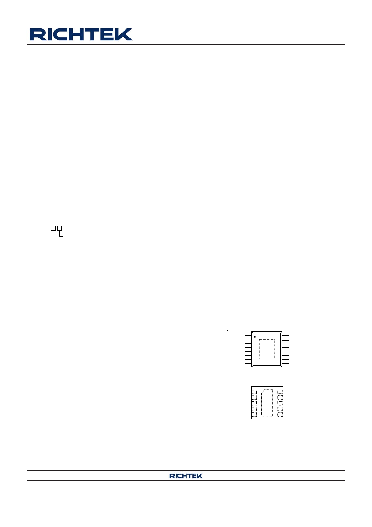
Pin Configurations
(TOP VIEW)
GND
8
VCC
7
PGOOD
6
9
EN
5
FB
BOOT
VIN
SW
GND
2
3
4
SOP-8 (Exposed Pad)
GND
11
10
GND
9
SW
8
SW
7
VIN
6
VIN
FB
PGOOD
EN
VCC
BOOT
1
2
3
4
5
WDFN-10L 3x3
Copyright 2014 Richtek Technology Corporation. All rights reserved. is a registered trademark of Richtek Technology Corporation.
©
DS8299-04 October 2014 www.richtek.com
1
Page 2
RT8299
Marking Information
RT8299GSP
RT8299GSP : Product Number
RT8299
YMDNN : Date Code
GSPYMDNN
RT8299ZSP
RT8299ZSP : Product Number
RT8299
YMDNN : Date Code
ZSPYMDNN
Typical Application Circuit
V
IN
Chip Enable
C
VCC
1µF
C
IN
10µF x 2
VIN
EN
VCC
GND
RT8299
BOOT
SW
FB
PGODD
RT8299GQW
56=YM
DNN
RT8299ZQW
56 YM
DNN
C
BOOT
R
T
Power Good
56= : Product Number
YMDNN : Date Code
56 : Product Number
YMDNN : Date Code
L1
R1
R2
C
OUT
V
OUT
Table 1. Recommended Component Selection
V
(V) R1 (k) R2 (k) RT (k) L (H) C
OUT
OUT
(F)
1.2 15 30 50 2 22 x 2
2.5 25.5 12 40 3.6 22 x 2
3.3 16 5.1 30 4.7 22 x 2
5 27 5.1 18 6.8 22 x 2
Copyright 2014 Richtek Technology Corporation. All rights reserved. is a registered trademark of Richtek Technology Corporation.
2
©
DS8299-04 October 2014www.richtek.com
Page 3
Functional Pin Description
Pin No.
SOP-8
(Exposed Pad)
1 5 BOOT
2 6, 7 VIN
3 8, 9 SW Switch Node. Connect to external LC filter.
4, 9
(Exp osed Pa d)
5 1 FB
6 3 EN
7 2 PGOOD Power Good Output. The output of this pi n is open drain.
8 4 VCC Bias Supply.
WDFN -1 0L 3x3
10, 11
(Exposed Pad)
Pin Name Pin Funct ion
GND
RT8299
Boot strap fo r High Si de Ga te D river. Connect a 0.1F or grea ter
ceramic capacitor from BOO T to SW pin.
Supply I nput Voltage. Must bypass wit h a suitably large ceram ic
capacitor.
Ground. The exposed pad mu st be sol der ed t o a large PCB and
connected to GND for maximum power dissipation.
Feedback Input. This pin is connected to the conv erter output . It
is used to regula te the output of the conver t er to a desired value
via an inter nal res istive voltage divider . F or an adj ustable output,
an external resistive voltage divider is connected to t his pin.
Enable Input. A logic high enables the converter; a logic low
forces the RT8299 into shutdown mode, reducing the supply
current to less than 3A. Attach th is pin to VIN with a 100k pul l
up resistor for aut oma tic startup.
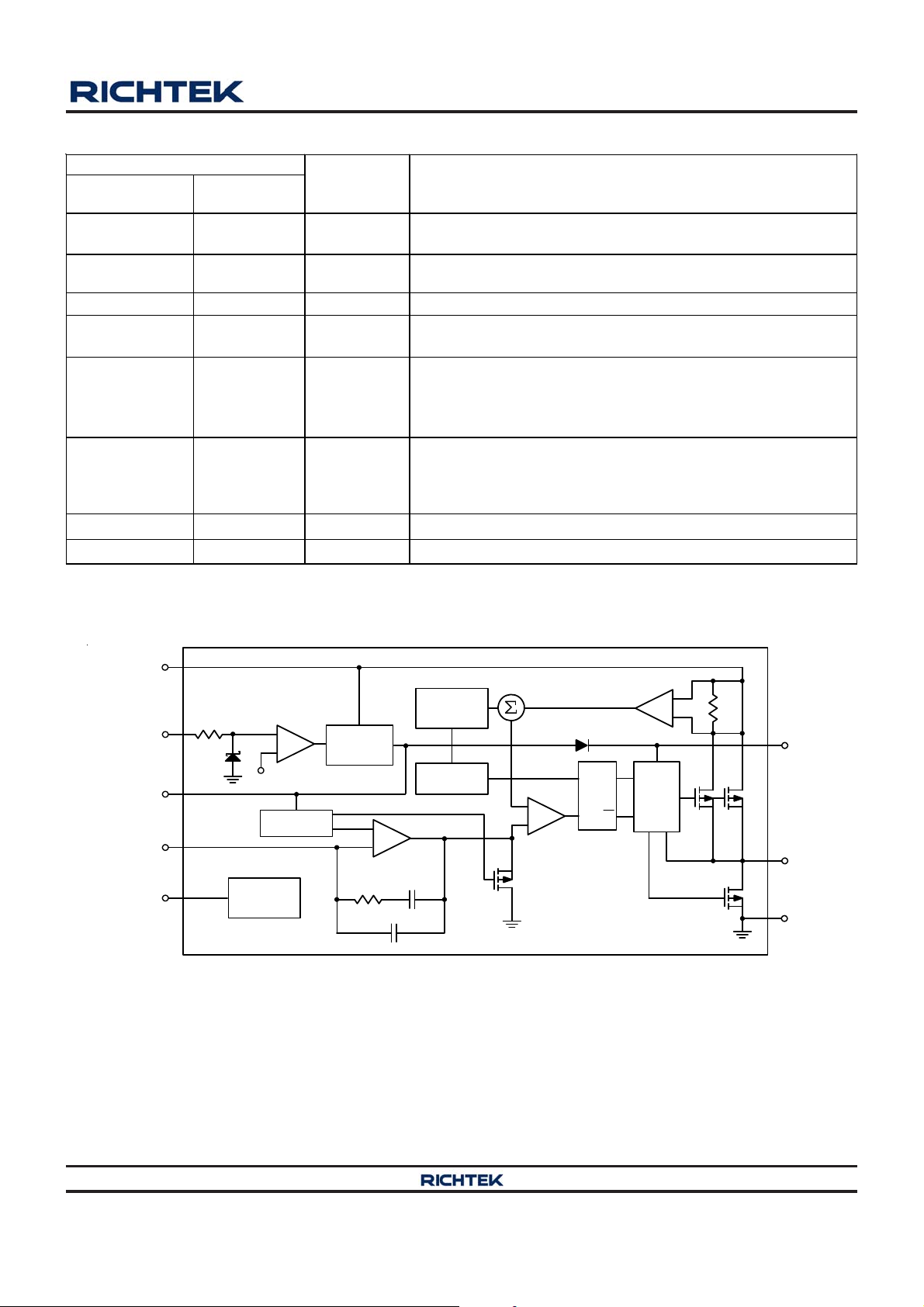
Function Block Diagram
VIN
Comparator
+
2V
Reference
PGOOD
Generator
EN
VCC
FB
PGOOD
5k
3V
Regulator
300k
+
-
Error
Amplifier
30pF
1pF
Ramp
Generator
Oscillator
500kHz
+
-
PWM
Comparator
OC Limit
Clamp
Current Sense
Amplifier
Q
S
Driver
Q
R
+
BOOT
SW
GND
Copyright 2014 Richtek Technology Corporation. All rights reserved. is a registered trademark of Richtek Technology Corporation.
DS8299-04 October 2014 www.richtek.com
©
3
Page 4
RT8299
Absolute Maximum Ratings (Note 1)
Supply Input V oltage, V
Switching Voltage, SW ------------------------------------------------------------------------------------ −0.6 to (V
---------------------------------------------------------------------------------- −0.3 to 26V
IN
+ 0.3V)
IN
< 20ns---------------------------------------------------------------------------------------------------------- −5V to 30V
Boot V oltage, BOOT---------------------------------------------------------------------------------------- (V
All Other Pins ------------------------------------------------------------------------------------------------ −0.3 to 6V
Power Dissipation, P
@ TA = 25°C
D
− 0.3V) to (VSW + 6V)
SW
SOP-8 (Exposed Pad) ------------------------------------------------------------------------------------- 1.333W
W D FN-10L 3x3 ----------------------------------------------------------------------------------------------- 1.429W
Package Thermal Re sistance (Note 2)
SOP-8 (Exposed Pad), θJA-------------------------------------------------------------------------------- 75°C/W
SOP-8 (Exposed Pad), θJC------------------------------------------------------------------------------- 15°C/W
W DFN-10L 3x3, θJA----------------------------------------------------------------------------------------- 70°C/W
WDFN-10L 3x3, θJC----------------------------------------------------------------------------------------- 8.2°C/W
Lead T e mperature (Soldering, 10 sec.)----------------------------------------------------------------- 260°C
Junction T e mperature -------------------------------------------------------------------------------------- 150°C
Storage T emperature Range ------------------------------------------------------------------------------ − 65°C to 150°C
ESD Susceptibility (Note 3)
HBM (Human Body Model)--------------------------------------------------------------------------------- 2kV
MM (Machine Model) ---------------------------------------------------------------------------------------- 200V
Recommended Operating Conditions (Note 4)
Supply Voltage, V
Junction T emperature Range------------------------------------------------------------------------------ − 40°C to 125°C
Ambient T emperature Range------------------------------------------------------------------------------ 40°C to 85°C
----------------------------------------------------------------------------------------- 3V to 24V
IN
Electrical Characteristics
(VIN = 12V, T
Shutdown Current I
Sup pl y Cu rrent VEN = 3V, V
Upper Switch On Resistance
Lower Switch On Resistance -- 100 -- m
Switch Leakage VEN = 0V, VSW = 0V o r 12V -- 0 10 A
Current Limit I
Oscillator Frequency f
Short Circuit Frequency VFB = 0V -- 150 -- kHz
M axi m um D ut y C ycl e D
Minimum On-Time tON -- 100 -- ns
Feedback Voltage VFB 4.5V VIN 24V 788 800 812 mV
EN Input
Threshold Voltage
Copyright 2014 Richtek Technology Corporation. All rights reserved. is a registered trademark of Richtek Technology Corporation.
4
= 25°C, unless otherwise specified)
A
Parameter Symbol Test Conditions Min Typ Max Unit
V
SHDN
V
LIM
VFB = 0.75V 425 500 575 kHz
OSC
VFB = 0.8V -- 93 -- %
MAX
Logic-High V
Logic-Low V
©
2 -- 5.5
IH
-- -- 0.4
IL
= 0V -- -- 3 A
EN
= 1V -- 1 -- mA
FB
-- 100 -- m
VSW = 4.8V -- 5.5 -- A
BOOT
V
DS8299-04 October 2014www.richtek.com
Page 5
RT8299
Parameter Symbol Test Conditions Min Typ Max Unit
Under Voltage Lockout
Threshold
Under Voltage Loc k out
Threshold Hysteresis
Power Good Threshold
VCC Regulator -- 5 -- V
VCC Load Regulation I
Soft-Start Period tSS -- 2 -- ms
Thermal Shutdown TSD -- 150 -- C
Note 1. Stresses beyond those listed “Absolute Maximum Ratings” may cause permanent damage to the device. These are
stress ratings only, and functional operation of the device at these or any other conditions beyond those indicated in
the operational sections of the specifications is not implied. Exposure to absolute maximum rating conditions may
affect device reliability.
Note 2. θ
Note 3. Devices are ESD sensitive. Handling precaution is recommended.
Note 4. The device is not guaranteed to function outside its operating conditions.
is measured at T
JA
measured at the exposed pad of the package.
= 25°C on a high effective thermal conductivity four-layer test board per JEDEC 51-7. θJC is
A
VIN Rising -- 2.8 -- V
V
UVLO
V
-- 300 -- mV
UVLO
VOUT Rising, with Respect to V
-- 90 --
FB
VOUT Falling, with Respect to VFB -- 70 --
= 5mA 4 -- 4 %
CC
%
Copyright 2014 Richtek Technology Corporation. All rights reserved. is a registered trademark of Richtek Technology Corporation.
DS8299-04 October 2014 www.richtek.com
©
5
Page 6

RT8299
Typical Operating Characteristics
Efficiency vs. Output Curre nt
100
90
80
70
60
50
40
Efficiency (% )
30
20
10
0
00.511.522.53
VIN = 5V, V
VIN = 12V, V
V
= 23V, V
IN
= 5V, V
V
IN
VIN = 3V, V
V
= 12V, V
IN
OUT
OUT
OUT
OUT
OUT
OUT
= 3.3V
= 3.3V
= 3.3V
= 1.2V
= 1.2V
= 1.2V
Output Current (A)
Reference Voltage vs. Temperature
0.820
0.815
0.810
0.805
Reference Voltage (V)
Reference Voltage vs. Input Voltage
0.820
0.815
0.810
0.805
0.800
0.795
0.790
0.785
V
= 3.3V, I
0.780
4 6 8 10 12 14 16 18 20 22 24
OUT
Input Voltage (V)
Output Voltage vs. Output Current
3.360
3.355
3.350
3.345
OUT
= 0A
Refer ence Voltage (V)
Output Voltage (V)
0.800
0.795
0.790
0.785
VIN = 12V, V
0.780
-50 -25 0 25 50 75 100 125
Temperature (°C)
Output Voltage vs. Output Current
1.240
1.235
1.230
1.225
1.220
1.215
1.210
1.205
V
= 1.2V
1.200
OUT
0 0.3 0.6 0.9 1.2 1.5 1.8 2.1 2.4 2.7 3
Output Current (A)
VIN = 3V
= 5VV
V
IN
VIN = 4.5V
V
= 12V
IN
OUT
= 3.3V
Output Voltage (V)
3.340
3.335
3.330
3.325
3.320
V
= 3.3V
OUT
0 0.3 0.6 0.9 1.2 1.5 1.8 2.1 2.4 2.7 3
VIN = 5V
= 12V
V
IN
V
= 23V
IN
Output Current (A)
Frequency vs. Input Voltage
570
560
550
540
530
520
510
500
Frequency ( kHz) 1
490
480
470
3 5 7 9 11 13 15 17 19 21 23
Inpu t Voltage (V)
V
OUT
= 1.2V, I
OUT
= 0.5A
Copyright 2014 Richtek Technology Corporation. All rights reserved. is a registered trademark of Richtek Technology Corporation.
©
DS8299-04 October 2014www.richtek.com
6
Page 7

RT8299
570
560
550
540
530
520
510
500
Frequency ( kHz) 1
490
480
470
V
OUT
(100mV/Div)
Frequency vs. Temperature
VIN = 23V
VIN = 12VV
V
= 5V
IN
V
= 3V
IN
-50 -25 0 25 50 75 100 125
V
OUT
= 1.2V, I
OUT
= 0.5A
Temperature (°C)
Load Transient Response
Current Limit (A)
V
OUT
(100mV/Div)
Current Limit vs. Temperature
8
7
6
5
4
3
2
-50 -25 0 25 50 75 100 125
VIN = 12V
= 5VV
V
IN
VIN = 3V
V
OUT
= 1.2V
Temperatur e (°C)
Load Transient Response
I
OUT
(2A/Div)
V
OUT
(5mV/Div)
V
SW
(10V/Div)
I
L
(2A/Div)
VIN = 12V, V
Time (100μs/Div)
Switching
VIN = 12V, V
Time (1μs/Div)
OUT
= 1.2V, I
= 1.2V, I
OUT
= 0A to 3A
OUT
OUT
= 3A
I
OUT
(2A/Div)
V
OUT
(5mV/Div)
V
SW
(10V/Div)
I
L
(2A/Div)
VIN = 12V, V
Time (100μs/Div)
Switching
VIN = 12V , V
Time (1μs/Div)
OUT
= 1.2V, I
OUT
= 1.5A to 3A
OUT
= 1.2V , I
OUT
= 1.5A
Copyright 2014 Richtek Technology Corporation. All rights reserved. is a registered trademark of Richtek Technology Corporation.
©
DS8299-04 October 2014 www.richtek.com
7
Page 8

RT8299
V
IN
(10V/Div)
V
OUT
(1V/Div)
I
L
(2A/Div)
V
EN
(5V/Div)
V
OUT
(1V/Div)
Power On from V
VIN = 12V, V
Time (2.5ms/Div)
OUT
=1.2V, I
Power On from EN
IN
V
IN
Power Off from V
IN
(10V/Div)
V
OUT
(1V/Div)
I
L
OUT
= 3A
(2A/Div)
VIN = 12V, V
= 1.2V, I
OUT
OUT
= 3A
Time (2.5ms/Div)
Power Off from EN
V
EN
(5V/Div)
V
OUT
(1V/Div)
I
L
(2A/Div)
VIN = 12V, V
= 1.2V, I
OUT
Time (2.5ms/Div)
OUT
= 3A
I
L
(2A/Div)
VIN = 12V, V
= 1.2V, I
OUT
Time (2.5ms/Div)
OUT
= 3A
Copyright 2014 Richtek Technology Corporation. All rights reserved. is a registered trademark of Richtek Technology Corporation.
©
DS8299-04 October 2014www.richtek.com
8
Page 9

Application Information
RT8299
The RT8299 is a synchronous high voltage buck converter
that can support the input voltage range from 3V to 24V
and the output current ca n be up to 3A.
Output Voltage Setting
The resistive divider allows the FB pin to sense the output
voltage as shown in Figure 1.
V
OUT
R1
FB
RT8299
GND
R2
Figure 1. Output Voltage Setting
The output voltage is set by an external resistive voltage
divider according to the following equation :
R1
V = V1
OUT FB
R2
where VFB is the feedback reference voltage (0.8V typ.).
External Bootstrap Diode
Chip Enable Operation
The EN pin is the chip enable input. Pulling the EN pin
low (<0.4V) will shutdown the device. During shutdown
mode, the RT8299 quiescent current drops to lower than
3μA. Driving the EN pin high (>2V, < 5.5V) will turn on the
device again. For external timing control (e.g.RC), the EN
pin can also be externally pulled high by adding a REN*
resistor and CEN* capacitor from the VIN pin (see Figure
5).
An external MOSFET can be a dded to implement digital
control on the EN pin when no system voltage above 2.5V
is available, a s shown in Figure 3. In this case, a 100kΩ
pull-up resistor, REN, is connected between VIN and the
EN pin. MOSFET Q1 will be under logic control to pull
down the EN pin.
V
IN
Chip Enable
R
100k
Q1
EN
VIN
C
IN
EN
VCC
C
GND
BOOT
RT8299
PGOOD
SW
FB
R
100k
C
BOOT
V
L
R1
R2
V
CC
OUT
C
OUT
Connect a 100nF low ESR ceramic capacitor between
the BOOT pin and SW pin. This capacitor provides the
gate driver voltage for the high side MOSFET.
It is recommended to add an external bootstrap diode
between an external 5V and BOOT pin for efficiency
improvement when input voltage is lower tha n 5.5V or duty
ratio is higher than 65% .The bootstrap diode can be a
low cost one such as IN4148 or BAT54. The external 5V
can be a 5V fixed in put from system or a 5V output of the
RT8299. Note that the external boot voltage must be lower
than 5.5V
5V
BOOT
RT8299
SW
0.1µF
Figure 2. External Bootstra p Diode
Figure 3. Enable Control Circuit for Logic Control with
Low V oltage
To prevent enabling circuit when VIN is smaller than the
V
target value, a resistive voltage divider can be pla ced
OUT
between the input voltage and ground a nd connected to
the EN pin to adjust IC lockout threshold, as shown in
Figure 4. For example, if a n 8V output voltage is regulated
from a 12V input voltage, the resistor R
can be selected
EN2
to set input lockout threshold larger than 8V.
V
12V
IN
R
EN
100k
R
EN2
C
IN
10µF
C
VIN
EN
VCC
GND
BOOT
RT8299
PGOOD
SW
FB
R
100k
C
BOOT
V
L
R1
R2
V
CC
Figure 4. The Resistors can be Selected to Set IC
OUT
8V
C
Lockout Threshold
Copyright 2014 Richtek Technology Corporation. All rights reserved. is a registered trademark of Richtek Technology Corporation.
DS8299-04 October 2014 www.richtek.com
©
OUT
9
Page 10

RT8299
Under Voltage Protection
Hiccup Mode
CIN and C
Selection
OUT
The input capacitance, C
is needed to filter the
IN,
trapezoidal current at the source of the high side MOSFET.
For the RT8299, it provides Hiccup Mode Under Voltage
Protection (UVP). When the FB voltage drops below half
of the feedback reference voltage, VFB, the UVP function
T o prevent large ripple current, a low ESR in put cap acitor
sized for the maximum RMS current should be used. The
RMS current is given by :
will be triggered and the RT8299 will shut down f or a period
of time and then recover automatically . The Hiccup Mode
UVP can reduce in put current in short-circuit conditions.
Inductor Selection
The inductor value and operating frequency determine the
ripple current according to a specific input and output
voltage. The ripple current ΔI
increases with higher V
L
and decrea ses with higher inducta nce.
VV
OUT OUT
I = 1
L
fL V
IN
Having a lower ripple current reduces not only the ESR
losses in the output capa citors but also the output voltage
ripple. High frequency with small ripple current ca n achieve
highest efficiency operation. However , it requires a large
V
I = I 1
RMS OUT(MAX)
OUT
VV
This formula has a maximum at V
I
= I
RMS
/ 2. This simple worst case condition is
OUT
commonly used for design because even significant
deviations do not offer much relief.
IN
Choose a capacitor rated at a higher temperature than
required. Several capacitors may also be paralleled to
meet size or height requirements in the design.
For the input capacitor, two 10μF low ESR ceramic
cap acitors are recommended.
The selection of C
OUT
to minimize voltage ripple.
V
IN
IN OUT
is determined by the required ESR
= 2V
IN
OUT
inductor to achieve this goal.
Moreover, the amount of bulk capacitance is also a key
For the ripple current selection, the value of ΔI
will be a reasonable starting point. The largest ripple
current occurs at the highest VIN. To guarantee that the
= 0.24(I
L
MAX
)
for C
selection to ensure that the control loop is stable.
OUT
Loop stability can be checked by viewing the loa d transient
response a s described in a later section.
ripple current stays below the specified maximum, the
inductor value should be chosen according to the following
equation :
VV
L = 1
OUT OUT
fI V
L(MAX) IN(MAX)
The inductor's current rating (caused a 40°C temperature
rising from 25°C ambient) should be greater than the
maximum load current and its saturation current should
be greater than the short circuit pea k current limit. Plea se
see Table 2 for the inductor selection reference.
Table 2. Suggested Inductors for Typical
Application Circuit
Compo nent
Supplier
Series
Dimension s
(mm)
TDK VLF10045 10 x 9.7 x 4.5
TDK SLF12565 12.5 x 12.5 x 6.5
TAIYO
YUDEN
NR8040 8 x 8 x 4
The output ripple, ΔV
VIESR
OUT L
The output ripple will be highest at the maximum input
voltage since ΔIL increases with input voltage. Multiple
cap a citors placed in parallel may be needed to meet the
ESR and RMS current ha ndling requirement. Dry ta ntalum,
special polymer, aluminum electrolytic and ceramic
capacitors are all available in surface mount packages.
Special polymer capacitors offer very low ESR value.
However, it provides lower ca pa citance density tha n other
types. Although Tantalum capacitors have the highest
cap a cita nce density, it is important to only use types that
pass the surge test for use in switching power supplies.
Aluminum electrolytic capa citors have significa ntly higher
ESR. However, it ca n be used in cost-sensitive application s
, is determined by :
OUT
1
8fC
OUT
Copyright 2014 Richtek Technology Corporation. All rights reserved. is a registered trademark of Richtek Technology Corporation.
10
©
DS8299-04 October 2014www.richtek.com
, where
Page 11

RT8299
for ripple current rating and long term reliability
considerations. Ceramic capacitors have excellent low
ESR characteristics but ca n have a high voltage coefficient
and audible piezoelectric effe cts. The high Q of ceramic
cap acitors with trace inducta nce can also lea d to significant
ringing.
Higher values, lower cost ceramic capacitors are now
becoming available in smaller ca se sizes. Their high ripple
current, high voltage rating and low ESR ma ke them ideal
for switching regulator a pplications. However , care must
be taken when these capacitors are used at input and
output. When a ceramic capacitor is used at the input
and the power is supplied by a wall ad a pter through long
wires, a load step at the output can induce ringing at the
input, VIN. At best, this ringing can couple to the output
and be mistaken as loop instability. At worst, a sudden
inrush of current through the long wires can potentially
cause a voltage spike at V
large enough to damage the
IN
part.
Checking Tra n sient Re spon se
The regulator loop response can be checked by looking
at the load transient respon se. Switching regulators take
several cycles to respond to a step in load current. When
a load step occurs, V
equal to ΔI
C
generating a feedback error signal f or the regulator
OUT
to return V
recovery time, V
(ESR) also begins to charge or discharge
LOAD
to its steady-state value. During this
OUT
OUT
immediately shifts by a n amount
OUT
can be monitored for overshoot or
ringing that would indicate a stability problem.
EMI Consideration
Since parasitic inducta nce and ca pa citance effects in PCB
circuitry would cause a spike voltage on SW pin when
high side MOSFET is turned-on/off, this spike voltage on
SW may impact on EMI performance in the system. In
order to enhance EMI performa nce, there are two methods
to suppress the spike voltage. One is to place an R-C
snubber between SW and GND and make them a s close
as possible to the SW pin (see Figure 5). Another method
is adding a resistor R
ca pacitor , C
. But this method will decrease the driving
BOOT
* in series with the bootstrap
BOOT
capability to the high side MOSFET. It is strongly
recommended to reserve the R-C snubber during PCB
layout for EMI improvement. Moreover , reducing the SW
trace area a nd keeping the main power in a small loop will
be helpful on EMI performa nce. For detailed PCB layout
guide, please refer to the se ction of Layout Consideration.
R
*
V
IN
REN*
CEN*
* : Optional
C
IN
10µF x 2
C
VIN
EN
VCC
GND
BOOT
RT8299
SW
FB
PGOOD
BOOT
R
100k
RS*
C
C
BOOT
L
*
S
V
CC
R1
R2
V
OUT
C
OUT
Figure 5. Reference Circuit with Snubber and Enable Timing Control
Copyright 2014 Richtek Technology Corporation. All rights reserved. is a registered trademark of Richtek Technology Corporation.
DS8299-04 October 2014 www.richtek.com
©
11
Page 12

RT8299
Thermal Considerations
For continuous operation, do not exceed the maximum
operation junction temperature 125°C. The maximum
power dissipation depends on the thermal resistance of
IC package, PCB layout, the rate of surroundings airflow
and temperature difference between junction to a mbient.
The maximum power dissipation can be calculated by
following formula :
P
Where T
temperature , T
D(MAX)
= (T
J(MAX)
− TA ) / θ
J(MAX)
JA
is the maximum operation junction
is the ambient temperature a nd the θ
A
JA
the junction to ambient thermal resistance.
For recommended operating condition specifications, the
maximum junction temperature is 125°C. The junction to
ambient thermal resista nce, θJA, is layout dependent. For
SOP-8 (Exposed Pad) package, the thermal resistance,
θ
, is 75°C/W on a standard JEDEC 51-7 four-layer
JA
thermal test board. For WDFN-10L 3x3 packageS, the
thermal resistance, θJA, is 70°C/W on a standard JEDEC
51-7 four-layer thermal test board. The maximum power
dissipation at TA = 25°C can be calculated by the following
formula s :
P
= (125°C − 25°C) / (75°C/W) = 1.333W for
D(MAX)
SOP-8 (Exposed Pad) package
P
= (125°C − 25°C) / (70°C/W) = 1.429W for
D(MAX)
W DF N-10L 3x3 pa ckage
The maximum power dissipation depends on the operating
ambient temperature for fixed T
and thermal
J(MAX)
resistance, θJA. The derating curve in Figure 6 allow the
designer to see the effect of rising ambient temperature
on the maximum power dissipation.
1.5
1.4
1.3
1.2
1.1
1.0
0.9
0.8
0.7
0.6
0.5
0.4
0.3
0.2
0.1
Maximum Power Dissipation (W) 1
0.0
is
SOP-8 (Exposed Pad)
0255075100125
WDFN-10L 3x3
Four-Layer PCB
Ambient Temperature (°C)
Figure 6. Derating Curve of Maxi mum Power Dissi pation
Layout Consideration
Follow the PCB layout guidelines for optimal performa nce
of the RT8299.
Keep the traces of the main current paths as short and
wide as possible.
Put the input ca pacitor a s close a s possible to the device
pins (VIN a nd GND).
SW node is with high frequency voltage swing a nd should
be kept at small area. Keep analog components away
from the SW node to prevent stray ca pacitive noise pickup.
Connect feedba ck network behind the output capa citors.
Keep the loop area small. Place the feedback
components near the RT8299.
An exa mple of PCB layout guide is shown in Figure 6 fo r
reference.
Copyright 2014 Richtek Technology Corporation. All rights reserved. is a registered trademark of Richtek Technology Corporation.
12
©
DS8299-04 October 2014www.richtek.com
Page 13

RT8299
GND
Input capacitor must
be placed as close
to the IC as possible.
V
SW should be connected to inductor by
wide and short trace. Keep sensitive
components away from this trace.
OUT
C
OUT
The C
as close to the device as possible.
SW
V
IN
C
IN
GND
BOOT
VIN
SW
*
C
GND
S
2
3
4
RS*
Figure 7. PCB Layout Guide
component must be connected
VCC
C
VCC
8
GND
VCC
7
PGOOD
6
9
EN
5
FB
R2
R
R
R1
V
The feedback components
must be connected as close
to the device as possible.
PG
V
CC
EN
V
IN
The R
must be connected to
VIN.
OUT
GND
component
EN
Copyright 2014 Richtek Technology Corporation. All rights reserved. is a registered trademark of Richtek Technology Corporation.
©
DS8299-04 October 2014 www.richtek.com
13
Page 14

RT8299
Outline Dimension
H
M
EXPOSED THERMAL PAD
(Bottom of Package)
A
Y
J
I
B
X
F
C
D
Dimensions In Millimeters Dim e nsions In Inches
Symbol
Min Max Min Max
A 4.801 5.004 0.189 0.197
B 3.810 4.000 0.150 0.157
C 1.346 1.753 0.053 0.069
D 0.330 0.510 0.013 0.020
H 0.170 0.254 0.007 0.010
M 0.406 1.270 0.016 0.050
Option 1
Option 2
F 1.194 1.346 0.047 0.053
I 0.000 0.152 0.000 0.006
J 5.791 6.200 0.228 0.244
X 2.000 2.300 0.079 0.091
Y 2.000 2.300 0.079 0.091
X 2.100 2.500 0.083 0.098
Y 3.000 3.500 0.118 0.138
8-Lead SOP (Exposed Pad) Plastic Package
Copyright 2014 Richtek Technology Corporation. All rights reserved. is a registered trademark of Richtek Technology Corporation.
14
©
DS8299-04 October 2014www.richtek.com
Page 15
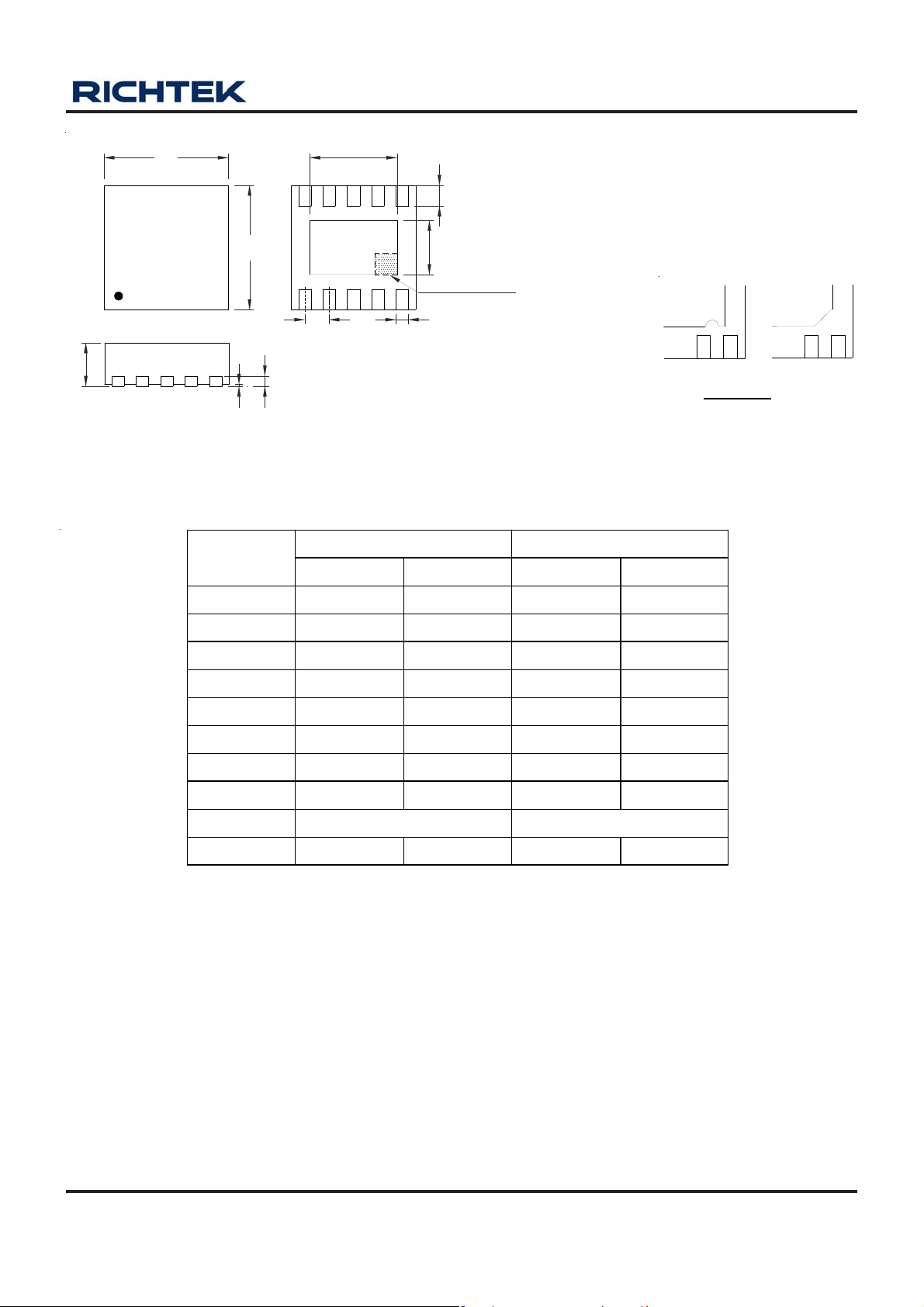
RT8299
D
E
A
A3
A1
D2
L
E2
SEE DETAIL A
1
e
b
2
1
1
2
DETAIL A
Pin #1 ID a nd T ie Bar Mark Option s
Note : The configuration of the Pin #1 identifier is optional,
but must be located within the zone indicated.
Dimensions In Millimeters Dimensions In Inches
Symbol
Min Max Min Max
A 0.700 0.800 0.028 0.031
A1 0.000 0.050 0.000 0.002
A3 0.175 0.250 0.007 0.010
b 0.180 0.300 0.007 0.012
D 2.950 3.050 0.116 0.120
D2 2.300 2.650 0.091 0.104
E 2.950 3.050 0.116 0.120
E2 1.500 1.750 0.059 0.069
e 0.500 0.020
L 0.350 0.450
Richtek Technology Corporation
14F, No. 8, Tai Yuen 1st Street, Chupei City
Hsinchu, Taiwan, R.O.C.
Tel: (8863)5526789
0.014 0.018
W-Type 10L DFN 3x3 Package
Richtek products are sold by description only. Richtek reserves the right to change the circuitry and/or specifications without notice at any time. Customers should
obtain the latest relevant information and data sheets before placing orders and should verify that such information is current and complete. Richtek cannot
assume responsibility for use of any circuitry other than circuitry entirely embodied in a Richtek product. Information furnished by Richtek is believed to be
accurate and reliable. However, no responsibility is assumed by Richtek or its subsidiaries for its use; nor for any infringements of patents or other rights of third
parties which may result from its use. No license is granted by implication or otherwise under any patent or patent rights of Richtek or its subsidiaries.
DS8299-04 October 2014 www.richtek.com
15
Page 16

 Loading...