

Page 1

RT8239A/B/C
®
DS8239A/B/C-06 October 2012 www.richtek.com
1
Copyright 2012 Richtek Technology Corporation. All rights reserved. is a registered trademark of Richtek Technology Corporation.
©
Ordering Information
Note :
Richtek products are :
` RoHS compliant and compatible with the current require-
ments of IPC/JEDEC J-STD-020.
` Suitable for use in SnPb or Pb-free soldering processes.
High Efficiency, Main Power Supply Controller
for Notebook Computers
General Description
The RT8239A/B/C is a dual step down, Switch Mode Power
Supply (SMPS) controller which generates logic supply
voltages for battery powered systems. It includes two
Pulse Width Modulation (PWM) controllers adjustable
from 2V to 5.5V and also two fixed 5V/3.3V linear
regulators. One of the controllers (LDO5) provides
automatic switch over to the BYP1 input connected to
the main SMPS1 output for maximized efficiency. An
optional external charge pump can be monitored through
SECFB (RT8239B/C). Other features include on board
power up sequencing, a power good output, internal soft-
start, and a soft discharge output that prevents negative
voltage during shutdown.
A constant on-time PWM control scheme operates without
sense resistors and assures fast load transient response
while maintaining nearly constant switching frequency. To
eliminate noise in audio applications, an ultrasonic mode
is included, which maintains the switching frequency
above 25kHz. Moreover, a diode emulation mode
maximizes efficiency for light load applications. The
SMPS1/SMPS2 switching frequency can be adjustable
from 200kHz/233kHz to 400kHz/466kHz respectively.
The RT8239A/B/C is available in a WQFN-20L 3x3
package, and operates over an extended temperature range
from −40°C to 85°C.
Features
zz
zz
z 5.5V to 25V Input Voltage Range
zz
zz
z 2V to 5.5V Output Voltage Range
zz
zz
z No Current Sense Resistor Needed
zz
zz
z 5V/3.3V Linear Regulators
zz
zz
z 4700ppm/
°°
°°
°C R
DS(ON)
Current Sensing
zz
zz
z Internal Current Limit Soft-Start and Soft Discharge
Output
zz
zz
z Built In OVP/UVP/OCP
zz
zz
z Selectable Operation Mode with Switcher Enable
Control (RT8239A)
zz
zz
z SECFB Input Maintains Charge Pump Voltage
(RT8239B/C)
zz
zz
z Power Good Indicator (RT8239B/C includes SECFB)
zz
zz
z RoHS Compliant and Halogen Free
Applications
z Notebook computers
z System Power Supplies
z 3- and 4- Cell Li+ Battery-Powered Device
RT8239A/B/C
Package Type
QW : WQFN-20L 3x3 (W-Type)
Lead Plating System
G : Green (Halogen Free and Pb Free)
Z : ECO (Ecological Element with
Halogen Free and Pb free)
Pin Function With
A : ENM
B : SECFB
C : SECFB, Ultrasonic Mode
Page 2
RT8239A/B/C
2
DS8239A/B/C-06 October 2012www.richtek.com
©
Copyright 2012 Richtek Technology Corporation. All rights reserved. is a registered trademark of Richtek Technology Corporation.
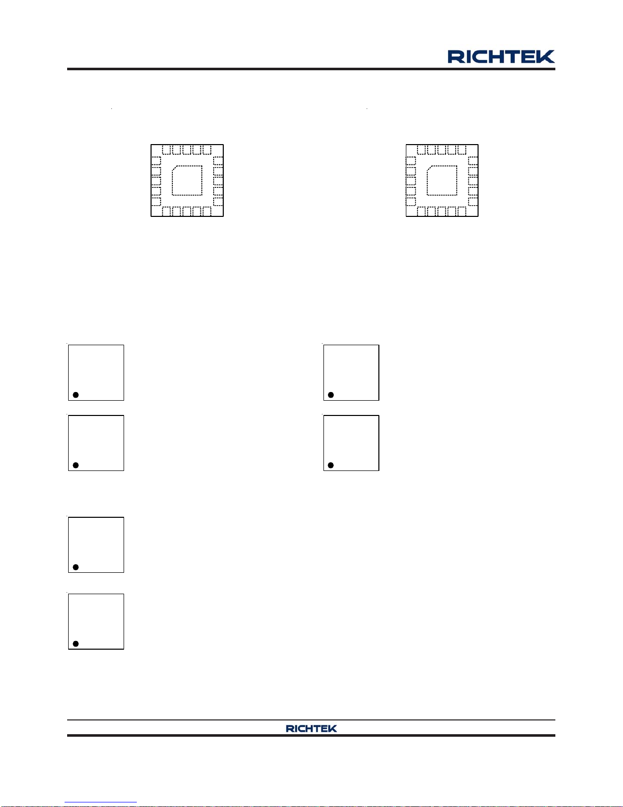
Pin Configurations
(TOP VIEW)
RT8239B/CRT8239A
WQFN-20L 3x3
BYP1
BOOT1
ENTRIP2
TON
FB1
ENTRIP1
LDO3
LDO5
ENLDO
ENM
PGOOD
BOOT2
PHASE2 PHASE1
UGATE1
LGATE1
FB2
VIN
LGATE2
UGATE2
15
14
13
12
17181920
1
2
3
4
9876
GND
21
115
16
10
LDO3
LDO5
ENTRIP2
TON
FB1
ENTRIP1
ENLDO
SECFB
PGOOD
BOOT2
PHASE2
BYP1
BOOT1
PHASE1
UGATE1
LGATE1
FB2
VIN
LGATE2
UGATE2
15
14
13
12
17181920
1
2
3
4
9876
GND
21
115
16
10
Marking Information
JB=YM
DNN
JB YM
DNN
JB= : Product Code
YMDNN : Date Code
JB : Product Code
YMDNN : Date Code
RT8239A
JC=YM
DNN
JC YM
DNN
JC : Product Code
YMDNN : Date Code
JC= : Product Code
YMDNN : Date Code
RT8239B
JD=YM
DNN
JD YM
DNN
JD : Product Code
YMDNN : Date Code
JD= : Product Code
YMDNN : Date Code
RT8239C
Page 3
RT8239A/B/C
3
DS8239A/B/C-06 October 2012 www.richtek.com
©
Copyright 2012 Richtek Technology Corporation. All rights reserved. is a registered trademark of Richtek Technology Corporation.
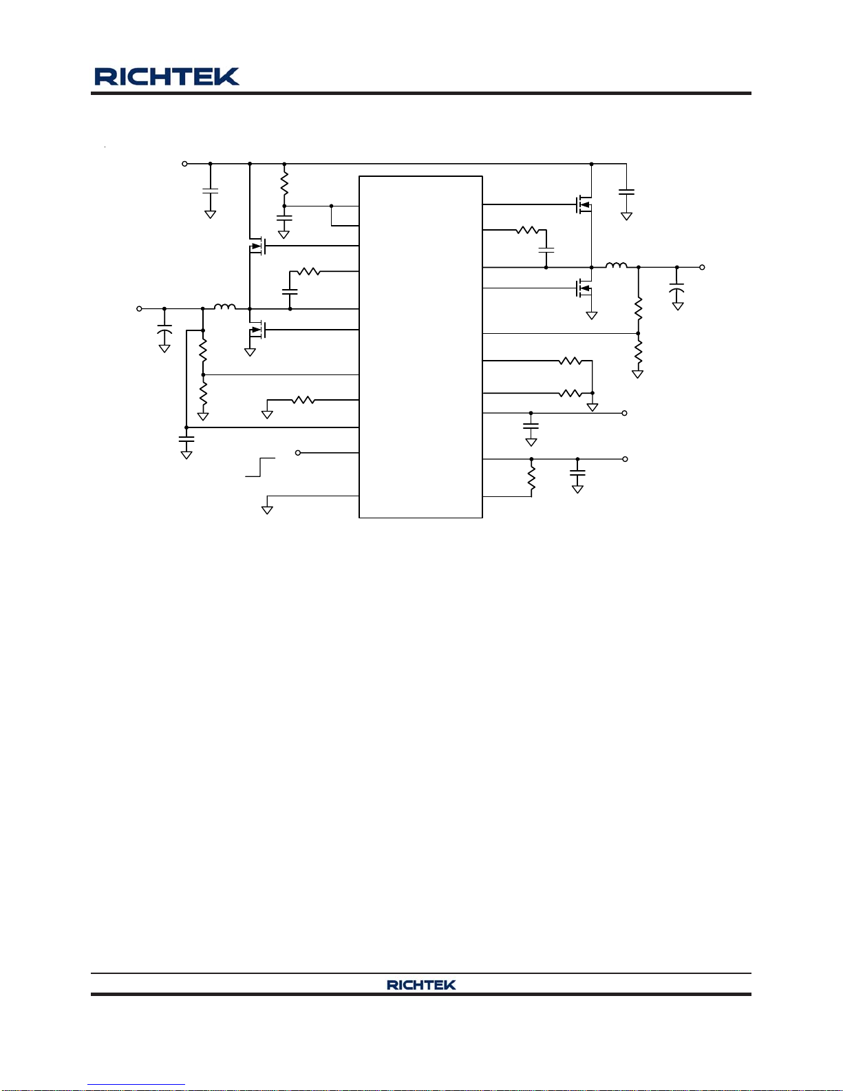
Typical Application Circuit
Figure 1. RT8239A NB Main Supply Typical Application Circuit
C
8
3
.
3
V
RT8239A
PHASE1
LGATE1
BOOT1
UGATE1
VIN
11
16
19
17
18
PHASE2
LGATE2
BOOT2
UGATE2
FB2
V
I
N
1
0
µ
F
8
9
7
10
5
C
6
R
1
C
2
0
.
1
µ
F
5
.
5
V
t
o
2
5
V
21 (Exposed Pad)
GND
N3
L
2
C
7
0
.
1
µ
F
R
5
N4
R
6
6
.
5
k
+
N1
L
1
C
4
C
3
5
V
0
.
1
µ
F
R
2
N2
R
3
1
5
k
+
R
4
1
0
k
R
7
1
0
k
FB1
1
BYP1
20
1
0
µ
F
C
1
ENLDO
12
R
8
1
0
0
k
R
9
1
0
0
k
ENTRIP2
4
ENTRIP1
2
LDO3
15
C
9
4
.
7
µ
F
LDO5
14
PGOOD
6
R10
100k
C10
5
V
A
l
w
a
y
s
O
n
TON
3
R
TON
ENM
13
C
5
1
µ
F
Chip Enable
3
.
3
V
A
l
w
a
y
s
O
n
V
O
U
T
2
V
O
U
T
1
10µF
Page 4
RT8239A/B/C
4
DS8239A/B/C-06 October 2012www.richtek.com
©
Copyright 2012 Richtek Technology Corporation. All rights reserved. is a registered trademark of Richtek Technology Corporation.
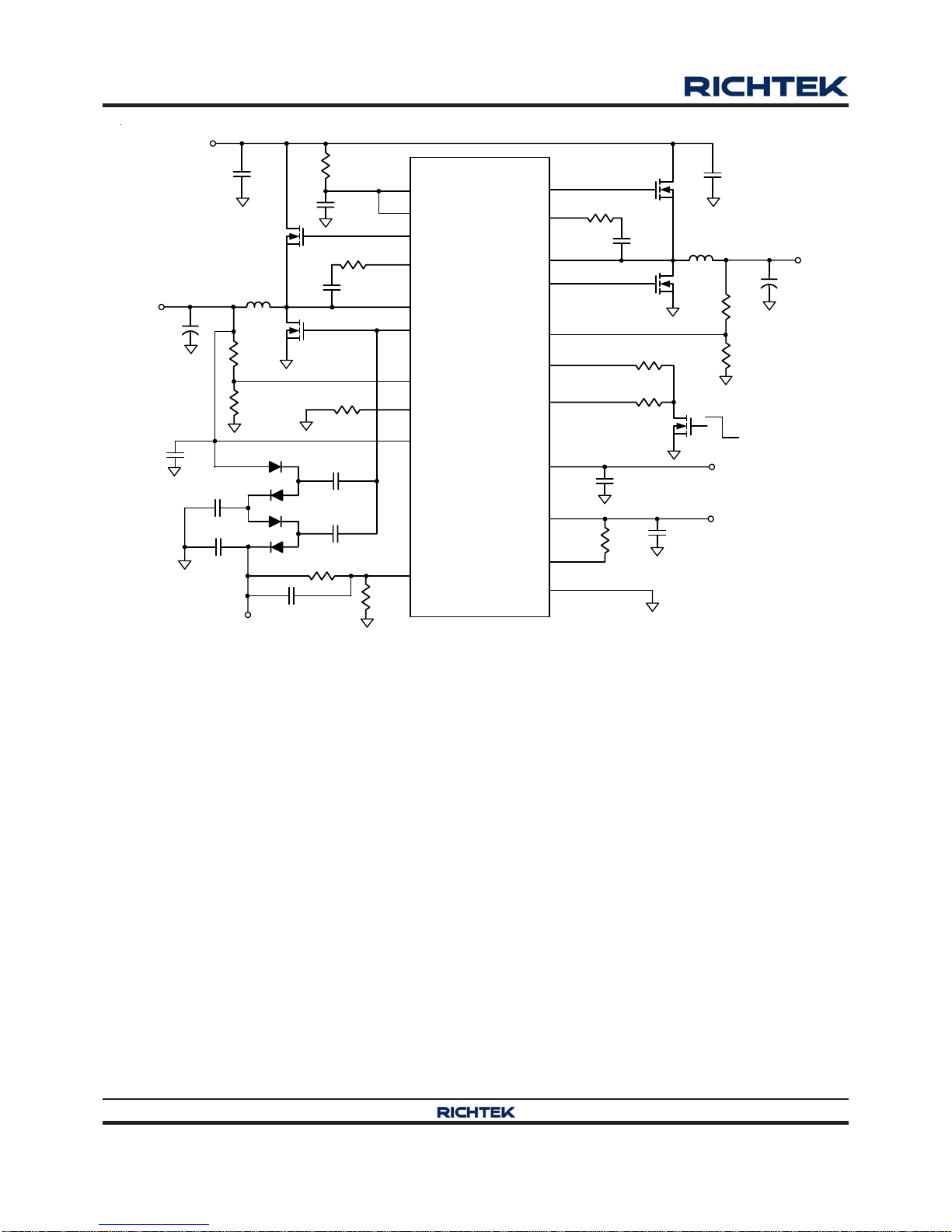
Figure 2. RT8239B/C NB Main Supply Typical Application Circuit
RT8239B/C
PHASE1
LGATE1
BOOT1
UGATE1
VIN
11
16
19
17
18
PHASE2
LGATE2
BOOT2
UGATE2
FB2
V
I
N
1
0
µ
F
8
9
7
10
5
C
6
R
1
C
2
0
.
1
µ
F
5
.
5
V
t
o
2
5
V
21 (Exposed Pad)
GND
N3
L
2
C
7
C
8
3
.
3
V
0
.
1
µ
F
R
5
N4
R
6
6
.
5
k
+
N1
L
1
C
4
C
3
5
V
0
.
1
µ
F
R
2
N2
R
3
1
5
k
+
R
4
1
0
k
R
7
1
0
k
FB1
1
BYP1
20
1
0
µ
F
C
1
ENLDO
12
R
8
1
0
0
k
R
9
1
0
0
k
ENTRIP2
4
ENTRIP1
2
Off
On
LDO3
15
C9
4.7µF
LDO5
14
PGOOD
6
R10
100k
C10
5
V
A
l
w
a
y
s
O
n
TON
3
R
TON
C
1
1
0
.
1
µ
F
C
1
2
0
.
1
µ
F
SECFB
13
R
1
1
2
0
0
k
R
1
2
3
9
k
V
CP
C
1
3
0
.
1
µ
F
C
1
4
0
.
1
µ
F
C
5
1
µ
F
C
1
5
3
.
3
V
A
l
w
a
y
s
O
n
V
O
U
T
1
V
O
U
T
2
10µF
Page 5
RT8239A/B/C
5
DS8239A/B/C-06 October 2012 www.richtek.com
©
Copyright 2012 Richtek Technology Corporation. All rights reserved. is a registered trademark of Richtek Technology Corporation.
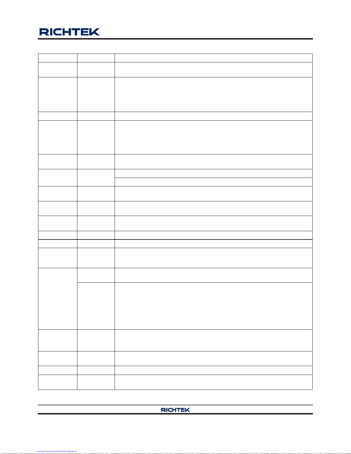
Pin No. Pin Name Pin Function
1 FB1
SMPS1 Feedback Input. Connect FB1 to a resistive voltage divider from SMPS1
output to GND for adjustable output from 2V to 5.5V.
2 ENTRIP1
Channel 1 Enable and Current Limit Setting Input. Connect resistor to GND to set
the threshold for Channel 1 synchronous R
DS(ON)
sense. The GND-PHASE1
current limit threshold is 1/10th the voltage seen at ENTRIP1 over a 0.5V to 3V
range. There is an internal 10μA current source from LDO5 to ENTRIP1. Leave
ENTRIP1 floating or drive it above 4.5V to shut down channel 1.
3 TON ON-Time/Frequency Adjustment Input. Connect to GND with 56kΩ to 100kΩ.
4 ENTRIP2
Channel 2 Enable and Current Limit Setting Input. Connect resistor to GND to set
the threshold for Channel 2 synchronous R
DS(ON)
sense. The GND-PHASE2
current limit threshold is 1/10th the voltage seen at ENTRIP2 over a 0.5V to 3V
range. There is an internal 10μA current source from LDO5 to ENTRIP2. Leave
ENTRIP2 floating or drive it above 4.5V to shut down channel 2.
5 FB2
SMPS2 Feedback Input. Connect FB2 to a resistive voltage divider from SMPS2
output to GND for adjustable output from 2V to 5.5V.
Power Good Output for Channel 1 and Channel 2 (RT8239A).
6 PGOOD
Power Good Output for Channel 1, Channel 2 and SECFB (RT8239B/C).
7 BOOT2
Boost Flying Capacitor Connection for SMPS2. Connect to an external capacitor
according to the typical application circuits.
8 UGATE2
Upper Gate Driver Output for SMPS2. UGATE2 swings between PHASE2 and
BOOT2.
9 PHASE2
Switch Node for SMPS2. PHASE2 is the internal lower supply rail for the UGATE2
high side gate driver. PHASE2 is also the current sense input for the SMPS2.
10 LGATE2 Lower Gate Drive Output for SMSP2. LGATE2 swings between GND and LDO5.
11 VIN Supply Input for LDO5.
12 ENLDO
Master Enable Input. LDO5/LDO3 is enabled if it is within logic high level and
disabled if it is less than the logic low level. Leave ENLDO floating to default
enable LDO5/LDO3.
ENM
(RT8239A)
Mode Selection with Enable Input. Pull up to LDO5 (Ultrasonic mode) or LDO3
(DEM) to turn on both switch Channels. Short to GND for shutdown.
13
SECFB
(RT8239B/C)
Change Pump Feedback Pin. The SECFB is used to monitor the optional external
charge pump. Connect a resistive divider from the change pump output to GND to
detect the output. If SECFB drops below its feedback threshold, an ultrasonic
pulse occurs to refresh the charge pump driven by LGATE1 or LGATE2.
If SECFB drops below its UV threshold, the switcher channels stop working and
enter into discharge-mode. Pull up to LDO5 or LDO3 to disable SECFB UVP
function.
14 LDO5
5V Linear Regulator Output. LDO5 is the supply voltage for the low side MOSFET
driver and also the analog supply voltage for the device. Bypass a minimum 4.7μF
ceramic capacitor to GND
15 LDO3
3.3V Linear Regulator Output. Bypass a minimum 4.7μF ceramic capacitor to
GND.
16 LGATE1 Lower Gate Driver Output for SMPS1. LGATE1 swings between GND and LDO5.
17 PHASE1
Switch Node SMPS1. PHASE1 is the internal lower supply rail for the UGATE1
high side gate driver. PHASE1 is also the current sense input for the SMPS1.
Functional Pin Description
Page 6
RT8239A/B/C
6
DS8239A/B/C-06 October 2012www.richtek.com
©
Copyright 2012 Richtek Technology Corporation. All rights reserved. is a registered trademark of Richtek Technology Corporation.
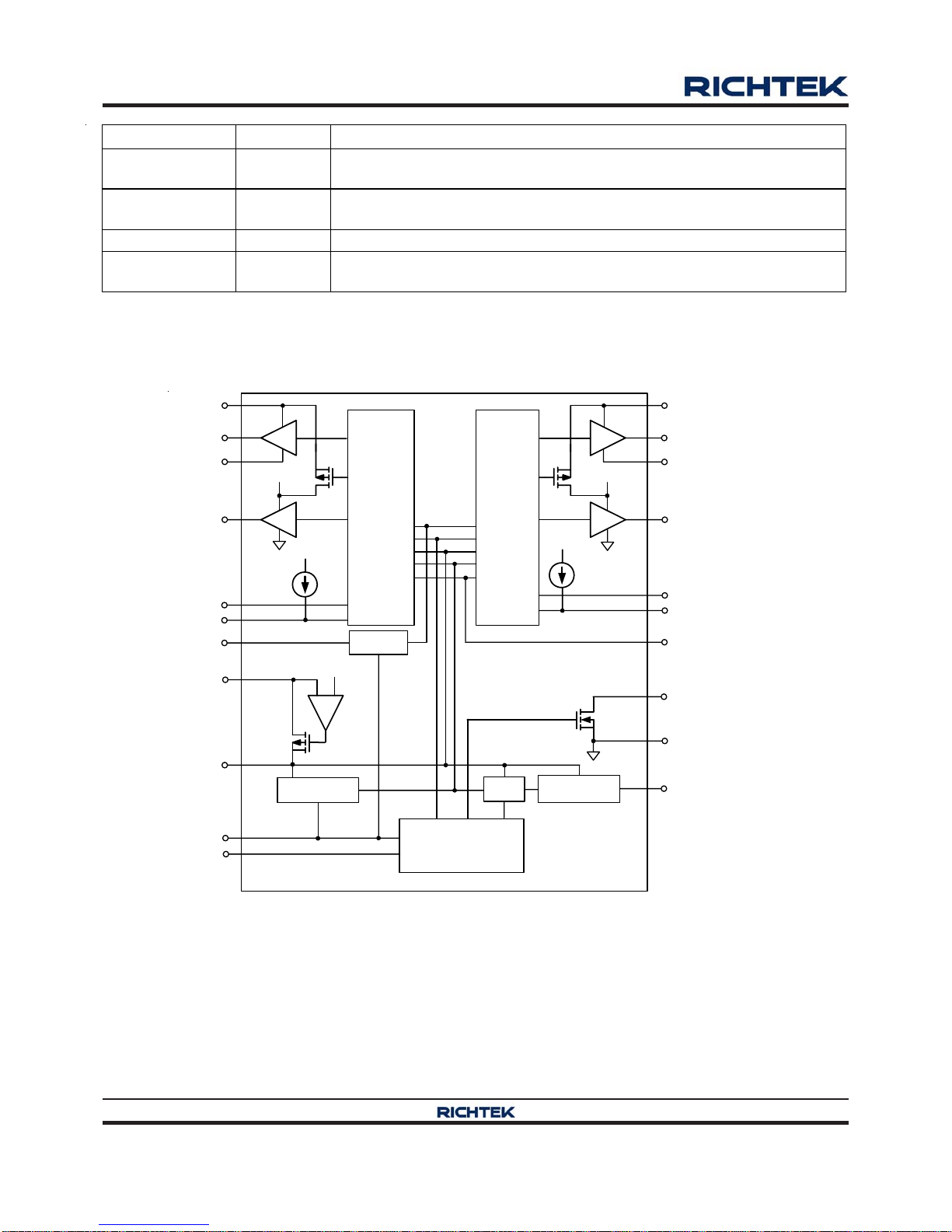
Function Block Diagram
Pin No. Pin Name Pin Function
18 UGATE1
Upper Gate Driver Output for SMPS1. UGATE1 swings between PHASE1 and
BOOT1.
19 BOOT1
Boost Flying Capacitor Connection for SMPS1. Connect to an external
capacitor according to the typical application circuits.
20 BYP1 Switch Over Source Voltage Input for LDO5.
21 (Exposed Pad) GND
Analog Ground and Power Ground. The exposed pad must be soldered to a
large PCB and connected to GND for maximum power dissipation.
ENM (RT8239A)
SECFB (RT8239B/C)
SMPS2
PWM
Buck
Controller
BOOT2
UGATE2
PHASE2
LGATE2
GND
LDO5
FB2
ENTRIP2
PGOOD
SMPS1
PWM
Buck
Controller
BOOT1
UGATE1
PHASE1
LGATE1
LDO5
FB1
ENTRIP1
LDO5
REF
Switch Over Threshold
VIN
LDO5
On Time
TON
LDO3
LDO3
BYP1
Power-On
Sequence
Clear Fault Latch
ENLDO
+
-
LDO5
10µA
LDO5
10µA
Page 7
RT8239A/B/C
7
DS8239A/B/C-06 October 2012 www.richtek.com
©
Copyright 2012 Richtek Technology Corporation. All rights reserved. is a registered trademark of Richtek Technology Corporation.
Recommended Operating Conditions (Note 4)
z Supply Input Voltage, VIN ----------------------------------------------------------------------------------------------- 5.5V to 25V
z Junction Temperature Range -------------------------------------------------------------------------------------------- −40°C to 125°C
z Ambient Temperature Range -------------------------------------------------------------------------------------------- −40°C to 85°C
Absolute Maximum Ratings (Note 1)
z VIN, ENLDO to GND ------------------------------------------------------------------------------------------------------ −0.3V to 30V
z BOOTx to PHASEx ------------------------------------------------------------------------------------------------------- −0.3V to 6V
z ENTRIPx, FBx, TON, BYP1, PGOOD, LDO5, LDO3, ENM/SECFB to GND ------------------------------- −0.3V to 6V
z PHASEx to GND
DC----------------------------------------------------------------------------------------------------------------------------- −0.3V to 30V
< 20ns ----------------------------------------------------------------------------------------------------------------------- −8V to 38V
z UGATEx to PHASEx
DC----------------------------------------------------------------------------------------------------------------------------- −0.3V to 6V
< 20ns ----------------------------------------------------------------------------------------------------------------------- −5V to 7.5V
z LGATEx to GND
DC----------------------------------------------------------------------------------------------------------------------------- −0.3V to 6V
< 20ns ----------------------------------------------------------------------------------------------------------------------- −2.5V to 7.5V
z Power Dissipation, P
D
@ TA = 25°C
WQFN-20L 3x3 ------------------------------------------------------------------------------------------------------------ 3.33W
z Package Thermal Resistance (Note 2)
WQFN-20L 3x3, θJA------------------------------------------------------------------------------------------------------- 30°C/W
WQFN-20L 3x3, θJC------------------------------------------------------------------------------------------------------ 7.5°C/W
z Lead Temperature (Soldering, 10 sec.) ------------------------------------------------------------------------------- 260°C
z Junction Temperature ----------------------------------------------------------------------------------------------------- 150°C
z Storage Temperature Range -------------------------------------------------------------------------------------------- −65°C to 150°C
z ESD Susceptibility (Note 3)
HBM (Human Body Model)---------------------------------------------------------------------------------------------- 2kV
Parameter Symbol Test Conditions Min Typ Max Unit
Input Supply
Rising Threshold -- 5.1 5.5
VIN Power On Reset
Falling Threshold 3.5 -- 4.5
V
VIN Shutdown Current
I
VIN_SHDN
V
ENLDO
= GND
-- 20 40
VIN Standby Supply Current
I
VIN_SBY
Both SMPS Off -- 250 350
μA
Quiescent Power Consumption
I
Q
Both SMPSs on, FBx = 2.1V,
BYP1 = 5V, ENM = 3.3V (RT8239A)
-- 5 7 mW
SMPS Output and FB Voltage
FBx, CCM Operation -- 2 --
FBx Regulation Voltage
V
FBx
FBx, DEM Operation 1.98 2.006 2.03
V
(VIN = 12V, V
ENLDO
= 5V, V
ENTRIPx
= 2V, V
BYP1
= 5V, No Load on LDO5, LDO3, T
A
= 25°C, unless otherwise specified)
Electrical Characteristics
Page 8
RT8239A/B/C
8
DS8239A/B/C-06 October 2012www.richtek.com
©
Copyright 2012 Richtek Technology Corporation. All rights reserved. is a registered trademark of Richtek Technology Corporation.
Parameter Symbol Test Conditions Min Typ Max Unit
Output Voltage Adjustable
Range
SMPS1, SMPS2 2 -- 5.5
SECFB Voltage
V
SECFB
RT8239B 1.92 2 2.08
V
On-Time
V
PHASE1
= 2V
-- 256 --
On-Time Pulse Width
t
UGATEx
V
IN
= 20V
R
TON
= 56kΩ
V
PHASE2
= 2V
-- 220 --
ns
Minimum Off-Time
t
LGATEx
V
FBx
= 1.8V
-- -- 400 ns
f
SMPS1
SMPS1 Operating Frequency 200 -- 400
Frequency Range
f
SMPS2
SMPS2 Operating Frequency 233 -- 466
kHz
Ultrasonic Mode Frequency
f
ASM
RT8239C, V
PHASEx
= 50mV
25 -- -- kHz
Soft-Start
Soft-Start Time
t
SSx
Zero to 200mV Current Limit Threshold
from ENTRIPx Enable
-- 2 -- ms
Current Sense
Current Limit Current Source
I
ENTRIPx
V
ENTRIPx
= 0.9V
9.4 10 10.6
μA
Temperature Coefficient of
I
ENTRIPx
On The Basis of 25°C
-- 4700 --
ppm/°C
Current Limit Adjustment
Range
V
ENTRIPx
= I
ENTRIPx
x R
ENTRIPx
0.5 -- 2.7 V
Current Limit Threshold
V
ENTRIPx
GND − PHASEx, V
ENTRIPx
= 2V
180 200 225 mV
Zero-Current Threshold
V
ZC
GND − PHASEx, FBx = 2.1V
-- 3 -- mV
Internal Regulator and Reference
V
BYP1
= 0V, I
LDO5
< 100mA
4.8 5 5.2
V
BYP1
= 0V, I
LDO5
< 100mA ,
6.5V < V
IN
< 25V
4.75 -- 5.25
LDO5 Output Voltage
V
LDO5
V
BYP1
= 0V, I
LDO5
< 50mA,
5.5V < V
IN
< 25V
4.75 -- 5.25
V
LDO5 Output Current I
SHORT5
V
BYP1
= 0V, V
LDO5
= 4.5V -- 225 -- mA
5V Switchover Threshold V
BYP1TH
Falling Edge, Rising Edge with FB1
Regulation Point
4.53 4.66 4.79 V
5V Switch R
DS(ON)
R
BYPSW
V
BYP1
= 5V, I
LDO5
= 50mA -- 1.5 3 Ω
V
BYP1
= 0V, I
LDO3
< 100mA 3.2 3.3 3.46 V
LDO3 Output Voltage V
LDO3
V
BYP1
= 5V, I
LDO3
< 100mA 3.2 3.3 3.46
LDO3 Output Current I
SHORT3
V
BYP1
= 0V, V
LDO3
= 2.9V -- 150 -- mA
UVLO
Rising Edge -- 4.35 4.5
LDO5 UVLO Threshold V
UVLO5
Falling Edge 3.9 4.05 4.2
V
LDO3 UVLO Threshold V
UVLO3
Both SMPS Off -- 2.2 --
Power Good
PGOOD Threshold V
PGOOD
PGOOD Detect, Rising edge with
soft-start delay time. Hysteresis = 2.5%
−14 −10 −6 %
PGOOD Propagation Delay t
PD_PGOOD
Falling Edge -- 5 -- μs
Page 9

RT8239A/B/C
9
DS8239A/B/C-06 October 2012 www.richtek.com
©
Copyright 2012 Richtek Technology Corporation. All rights reserved. is a registered trademark of Richtek Technology Corporation.
Parameter Symbol Test Conditions Min Typ Max Unit
PGOOD Leakage Current I
LK_PGOOD
High State, Forced to 5.5V -- -- 1 μA
PGOOD Output Low Voltage V
SINK_PGOOD ISINK
= 4mA -- -- 0.4 V
SECFB Power Good
Threshold
V
SFB_PGOOD
SECFB with Respect to 2V
(RT8239B/C)
40 50 60 %
Fault Detection
Over Voltage Protection Trip
Threshold
V
OVP
OVP Detect, FBx Rising Edge 108 112 116 %
Over Voltage Protection
Propagation Delay
t
DLY_OVP
Rising Edge -- 5 -- μs
V
UVP
UVP Detect, FBx Falling Edge. 53 58 63 %
Under Voltage Protection Trip
Threshold
V
SFB_UVP
UVP Detect, SECFB Falling Edge. 0.8 -- 1.2 V
Under Voltage Protection
Shutdown Blanking Time
t
SSHx
From ENTRIPx or ENM Enable -- 5 -- ms
Thermal Shutdow n
Thermal Shutdown TSD -- 150 -- °C
Thermal Shutdown Hysteresis ΔTSD -- 10 -- °C
Logic Input
ENTRIPx Input Voltage V
ENTRIPx
Clear Fault Level/SMPSx Off Level 4.5 -- -- V
Rising Edge Threshold 1.2 1.6 2
Falling Edge Threshold 0.9 0.95 1
ENLDO Input Voltage V
ENLDO
When ENLDO is Floating (Default
Enable)
2.1 -- --
V
Clear Fault Level/SMPSs Off Level -- -- 0.8
SMPSs On, DEM Operation 2.3 -- 3.6
ENM Input Voltage
(RT8239A)
V
ENM
SMPSs On, Ultrasonic Mode
Operation
4.5 -- --
V
I
FBx
V
FBx
= 0V or 5V −1
-- 1
I
P13
ENM/SECFB = 0V or 5V
−1
-- 1
Input Leakage Current
I
ENLDO
ENLDO = 0V or 5V
−1
-- 3
μA
Internal BOOT Switch
Internal Boost Charging
Switch On-Resistance
R
BOOTx
LDO5 to BOOTx, 10mA -- -- 90
Ω
Power MOSFET Drivers
R
UGATEsr
Source, V
BOOTx
− V
UGATEx
= 0.1V
-- 5 8
UGATEx On-Resistance
R
UGATEsk
Sink, V
UGATEx
− V
PHAS Ex
= 0.1V
-- 2 4
Ω
R
LGATEsr
Source, V
LDO5
− V
LGATEx
= 0.1V
-- 5 8
LGATEx On-Resistance
R
LGATEsk
Sink, V
LGATEx
= 0.1V
-- 1.5 3
Ω
t
LGATERx
UGATEx Off to LGATEx On -- 30 --
Dead Time
t
UGATERx
LGATEx Off to UGATEx On -- 40 --
ns
Page 10

RT8239A/B/C
10
DS8239A/B/C-06 October 2012www.richtek.com
©
Copyright 2012 Richtek Technology Corporation. All rights reserved. is a registered trademark of Richtek Technology Corporation.
Note 1. Stresses beyond those listed “Absolute Maximum Ratings” may cause permanent damage to the device. These are
stress ratings only, and functional operation of the device at these or any other conditions beyond those indicated in
the operational sections of the specifications is not implied. Exposure to absolute maximum rating conditions may
affect device reliability.
Note 2. θ
JA
is measured at T
A
= 25°C on a high effective thermal conductivity four-layer test board per JEDEC 51-7. θJC is
measured at the exposed pad of the package.
Note 3. Devices are ESD sensitive. Handling precaution is recommended.
Note 4. The device is not guaranteed to function outside its operating conditions.
Page 11
RT8239A/B/C
11
DS8239A/B/C-06 October 2012 www.richtek.com
©
Copyright 2012 Richtek Technology Corporation. All rights reserved. is a registered trademark of Richtek Technology Corporation.
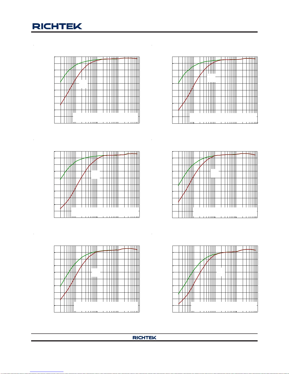
Typical Operating Characteristics
V
OUT2
Efficiency vs. Load Current
0
10
20
30
40
50
60
70
80
90
100
0.001 0.01 0.1 1 10
Load Current (A)
Efficiency (%)
VIN = 12V, R
TON
= 100kΩ, V
ENTRIP1
= 5V,
V
ENTRIP2
= 1.5V, ENLDO = 5V
DEM
ASM
V
OUT2
Efficiency vs. Load Current
0
10
20
30
40
50
60
70
80
90
100
0.001 0.01 0.1 1 10
Load Current (A)
Efficiency (%)
VIN = 20V, R
TON
= 100kΩ, V
ENTRIP1
= 5V,
V
ENTRIP2
= 1.5V, ENLDO = 5V
DEM
ASM
V
OUT2
Efficiency vs. Load Current
0
10
20
30
40
50
60
70
80
90
100
0.001 0.01 0.1 1 10
Load Current (A)
Efficiency (%)
VIN = 8V, R
TON
= 100kΩ, V
ENTRIP1
= 5V,
V
ENTRIP2
= 1.5V, ENLDO = 5V
DEM
ASM
V
OUT1
Efficiency vs. Load Current
0
10
20
30
40
50
60
70
80
90
100
0.001 0.01 0.1 1 10
Load Current (A)
Efficiency (%)
VIN = 20V, R
TON
= 100kΩ, V
ENTRIP1
= 1.5V
V
ENTRIP2
= 5V, ENLDO = 5V
DEM
ASM
V
OUT1
Efficiency vs. Load Current
0
10
20
30
40
50
60
70
80
90
100
0.001 0.01 0.1 1 10
Load Current (A)
Efficiency (%)
VIN = 8V, R
TON
= 100kΩ, V
ENTRIP1
= 1.5V
V
ENTRIP2
= 5V, ENLDO = 5V
DEM
ASM
V
OUT1
Efficiency vs. Load Current
0
10
20
30
40
50
60
70
80
90
100
0.001 0.01 0.1 1 10
Load Current (A)
Efficiency (%)
VIN = 12V, R
TON
= 100kΩ, V
ENTRIP1
= 1.5V
V
ENTRIP2
= 5V, ENLDO = 5V
DEM
ASM
Page 12

RT8239A/B/C
12
DS8239A/B/C-06 October 2012www.richtek.com
©
Copyright 2012 Richtek Technology Corporation. All rights reserved. is a registered trademark of Richtek Technology Corporation.
V
OUT1
Switching Frequency vs . Loa d Current
0
20
40
60
80
100
120
140
160
180
200
220
240
0.001 0.01 0.1 1 10
Load Current (A)
Switching Frequency (kHz) 1
VIN = 8V, R
TON
= 100kΩ,
ENLDO = VIN, V
ENTRIP1
= 1.5V,
V
ENTRIP2
= 5V
ASM
DEM
V
OUT1
Switching Frequency v s . Load Current
0
20
40
60
80
100
120
140
160
180
200
220
240
260
0.001 0.01 0.1 1 10
Load Current (A)
Switch Frequency (kHz) 1
VIN = 12V, R
TON
= 100kΩ,
ENLDO = VIN, V
ENTRIP1
= 1.5V,
V
ENTRIP2
= 5V
ASM
DEM
V
OUT1
Switching Frequency v s. Loa d Current
0
20
40
60
80
100
120
140
160
180
200
220
240
260
0.001 0.01 0.1 1 10
Load Current (A)
Switching Frequency (kHz) 1
VIN = 20V, R
TON
= 100kΩ,
ENLDO = VIN, V
ENTRIP1
= 1.5V,
V
ENTRIP2
= 5V
ASM
DEM
V
OUT2
Switching Frequency vs . Loa d Current
0
20
40
60
80
100
120
140
160
180
200
220
240
260
280
300
0.001 0.01 0.1 1 10
Load Current (A)
Switching Frequency (kHz) 1
VIN = 12V, R
TON
= 100kΩ,
ENLDO = VIN, V
ENTRIP1
= 5V,
V
ENTRIP2
= 1.5V
ASM
DEM
V
OUT2
Switching Frequency vs . Loa d Current
0
20
40
60
80
100
120
140
160
180
200
220
240
260
280
300
0.001 0.01 0.1 1 10
Load Current (A)
Switching Frequency (kHz) 1
VIN = 20V, R
TON
= 100kΩ,
ENLDO = VIN, V
ENTRIP1
= 5V,
V
ENTRIP2
= 1.5V
ASM
DEM
V
OUT2
Switching Frequency v s . Loa d Current
0
20
40
60
80
100
120
140
160
180
200
220
240
260
280
0.001 0.01 0.1 1 10
Load Current (A)
Switching Frequency (kHz) 1
VIN = 8V, R
TON
= 100kΩ,
ENLDO = VIN, V
ENTRIP1
= 5V,
V
ENTRIP2
= 1.5V
ASM
DEM
Page 13

RT8239A/B/C
13
DS8239A/B/C-06 October 2012 www.richtek.com
©
Copyright 2012 Richtek Technology Corporation. All rights reserved. is a registered trademark of Richtek Technology Corporation.
V
OUT2
Output Voltage vs. Load Current
3.372
3.378
3.384
3.390
3.396
3.402
3.408
3.414
3.420
0.001 0.01 0.1 1 10
Load Current (A)
Output Voltage (V)
VIN = 12V, R
TON
= 100kΩ, ENLDO = VIN,
V
ENTRIP1
= 5V, V
ENTRIP2
= 1.5V
ASM
DEM
V
OUT1
Output Voltage vs. Load Current
5.010
5.013
5.016
5.019
5.022
5.025
5.028
5.031
5.034
0.001 0.01 0.1 1 10
Load Curre nt (A)
Output Voltage (V)
VIN = 12V, R
TON
= 100kΩ, ENLDO = VIN,
V
ENTRIP1
= 1.5V, V
ENTRIP2
= 5V
ASM
DEM
Standby Input Current vs. Input Voltage
226
228
230
232
234
236
238
240
6 8 10 12 14 16 18 20 22 24 26
Input Voltage (V)
Standby Input Current (μA) 1
V
ENTRIP1
= V
ENTRIP2
= 5V, ENLDO = VIN, No Load
LDO5 Output Voltage vs. Output Current
5.048
5.052
5.056
5.060
5.064
5.068
5.072
0 102030405060708090100
Output Current (mA)
Output Voltage (V)
VIN = 12V, V
ENTRIP1
= V
ENTRIP2
= 5V, ENLDO = VIN
LDO3 Output Voltage vs. Output Current
3.334
3.336
3.338
3.340
3.342
3.344
3.346
3.348
3.350
3.352
3.354
0 102030405060708090100
Output Current (mA)
Output Voltage (V)
VIN = 12V, V
ENTRIP1
= V
ENTRIP2
= 5V, ENLDO = VIN
No Load Battery Current vs. Input Voltage
0.1
1
10
100
6 7 8 9 10111213141516171819202122232425
Input Voltage (V)
Battery Current (mA
)
R
TON
= 100kΩ, V
ENTRIP1
= V
ENTRIP2
=1.5V,
EVLDO = VIN
ASM
DEM
Page 14

RT8239A/B/C
14
DS8239A/B/C-06 October 2012www.richtek.com
©
Copyright 2012 Richtek Technology Corporation. All rights reserved. is a registered trademark of Richtek Technology Corporation.
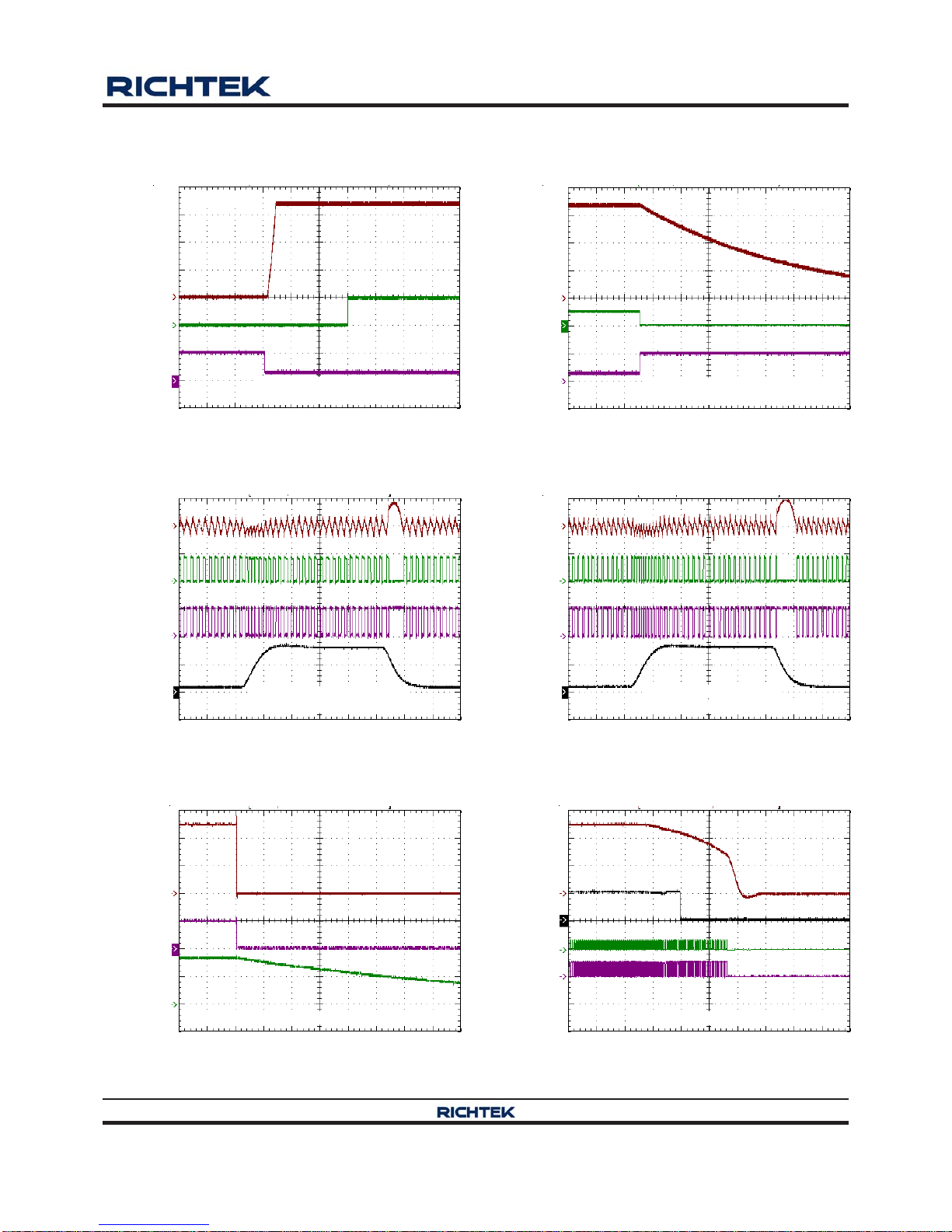
Power On from ENLDO
Time (2ms/Div)
VIN = 12V, V
ENTRIP1
= V
ENTRIP2
= 1.5V
LDO5
(2V/Div)
LDO3
(2V/Div)
ENLDO
(10V/Div)
CP
(10V/Div)
ENLDO = VIN, R
TON
= 100kΩ, No Load
Shutdown Input Current vs. Input Voltage
10
11
12
13
14
15
16
17
18
19
20
21
22
6 8 10 12 14 16 18 20 22 24 26
Input Voltage (V)
Shutdown Input Current (μA) 1
V
ENTRIP1
= V
ENTRIP2
= 5V, ENLDO = GND, No Load
Power Off from ENTRIP1
Time (4ms/Div)
RT8239B/C
VIN = 12V, V
ENTRIP1
= V
ENTRIP2
= 1.5V,
ENLDO = VIN, R
TON
= 100kΩ, No Load
VIN = 12V, V
ENTRIP1
= V
ENTRIP2
= 1.5V,
ENLDO = VIN, R
TON
= 100kΩ, No Load
V
OUT1
(2V/Div)
PGOOD
(5V/Div)
ENTRIP1
(5V/Div)
RT8239B/C
Power On from ENTRIP1
Time (1ms/Div)
VIN = 12V, V
ENTRIP1
= V
ENTRIP2
= 1.5V,
ENLDO = VIN, R
TON
= 100kΩ, No Load
V
OUT1
(2V/Div)
PGOOD
(5V/Div)
ENTRIP1
(5V/Div)
RT8239B/C
Power Off from ENM
Time (10ms/Div)
V
OUT1
(5V/Div)
PGOOD
(5V/Div)
ENM
(5V/Div)
V
OUT2
(5V/Div)
RT8239A
VIN = 12V, V
ENM
= 5V, R
TON
= 100kΩ,
V
ENTRIP1
= V
ENTRIP2
= 1.5V,
ENLDO = VIN, No Load
Power On from ENM
Time (1ms/Div)
V
OUT1
(2V/Div)
PGOOD
(5V/Div)
ENM
(5V/Div)
RT8239A
V
OUT2
(2V/Div)
V
ENTRIP1
= V
ENTRIP2
= 1.5V, ENLDO = VIN, No Load
VIN = 12V, V
ENM
= 5V, R
TON
= 100kΩ
Page 15
RT8239A/B/C
15
DS8239A/B/C-06 October 2012 www.richtek.com
©
Copyright 2012 Richtek Technology Corporation. All rights reserved. is a registered trademark of Richtek Technology Corporation.
OVP
Time (10ms/Div)
VIN = 12V, R
TON
= 100kΩ, ENLDO = VIN, No Load
V
OUT1
(2V/Div)
PGOOD
(5V/Div)
V
OUT2
(2V/Div)
UVP
Time (100μs/Div)
VIN = 12V, R
TON
= 100kΩ, ENLDO = VIN
V
OUT1
(2V/Div)
LGATE1
(10V/Div)
UGATE1
(50V/Div)
PGOOD
(5V/Div)
V
OUT2
DEM-MODE Load Transient Response
Time (20μs/Div)
ENLDO = VIN, I
OUT2
=1A to 8A
V
OUT2_AC
(50mV/Div)
Inductor
Current
(5A/Div)
UGATE2
(20V/Div)
LGATE2
(5V/Div)
VIN = 12V, R
TON
= 100kΩ,
Power Off from ENTRIP2
Time (20ms/Div)
VIN = 12V, V
ENTRIP1
= V
ENTRIP2
= 1.5V,
ENLDO = VIN, R
TON
= 100kΩ, No Load
V
OUT2
(1V/Div)
PGOOD
(10V/Div)
ENTRIP2
(5V/Div)
RT8239B/C
V
OUT1
DEM-MODE Load Transient Response
Time (20μs/Div)
VIN = 12V, R
TON
= 100kΩ,
ENLDO = VIN, I
OUT1
=1A to 8A
V
OUT1_AC
(50mV/Div)
Inductor
Current
(5A/Div)
UGATE1
(20V/Div)
LGATE1
(5V/Div)
Power On from ENTRIP2
Time (1ms/Div)
VIN = 12V, V
ENTRIP1
= V
ENTRIP2
= 1.5V,
ENLDO = VIN, R
TON
= 100kΩ, No Load
V
OUT2
(1V/Div)
PGOOD
(5V/Div)
ENTRIP2
(5V/Div)
RT8239B/C
Page 16

RT8239A/B/C
16
DS8239A/B/C-06 October 2012www.richtek.com
©
Copyright 2012 Richtek Technology Corporation. All rights reserved. is a registered trademark of Richtek Technology Corporation.
Application Information
The RT8239A/B/C is a dual, Mach Response
TM
DRV
TM
mode synchronous buck controller targeted for notebook
system power supply solutions. RICHTEK's Mach
ResponseTM technology provides fast response to load
steps. The topology circumvents the poor load transient
timing problems of fixed frequency current mode PWMs
while avoiding the problems caused by widely varying
switching frequency in conventional constant on-time and
constant off-time PWM schemes. A special adaptive on-
time control trades off the performance and efficiency over
wide input voltage range. The RT8239A/B/C includes 5V
(LDO5) and 3.3V (LDO3) linear regulators. The LDO5 linear
regulator steps down the battery voltage to supply both
internal circuitry and gate drivers. The synchronous switch
gate drivers are directly powered by LDO5. When V
OUT1
rises above 4.66V, an automatic circuit disconnects the
linear regulator and allows the device to be powered by
V
OUT1
via the BYP1 pin.
PWM Operation
The Mach ResponseTM DRV
TM
mode controller relies on
the output filter capacitor's Effective Series Resistance
(ESR) to act as a current sense resistor, so that the output
ripple voltage provides the PWM ramp signal. Referring to
the RT8239A/B/C's Function Block Diagram, the
synchronous high side MOSFET will be turned on at the
beginning of each cycle. After the internal one-shot timer
expires, the MOSFET will be turned off. The pulse width
of this one-shot is determined by the converter's input
voltage and the output voltage to keep the frequency fairly
constant over the entire input voltage range. Another one-
shot sets a minimum off-time (400ns typ). The on-time
one-shot will be triggered if the error comparator is high,
the low side switch current is below the current limit
threshold, and the minimum off-time one-shot has timed
out.
PWM Frequency and On-time Control
For each specific input voltage range, the Mach
ResponseTM control architecture runs with pseudo constant
frequency by feed forwarding the input and output voltage
into the on-time one-shot timer. The high side switch on-
time is inversely proportional to the input voltage as
measured by VIN and proportional to the output voltage.
There are two benefits of a constant switching frequency.
First, the frequency can be selected to avoid noise
sensitive regions such as the 455kHz IF band. Second,
the inductor ripple current operating point remains
relatively constant, resulting in easy design methodology
and predictable output voltage ripple. The frequency for
3V SMPS is set higher than the frequency for 5V SMPS.
This is done to prevent audio frequency “beating” between
the two sides, which switch asynchronously for each side.
The TON pin is connected to GND through the external
resistor, R
TON
, to set the switching frequency.
The RT8239A/B/C adaptively changes the operation
frequency according to the input voltage. Higher input
voltage usually comes from an external adapter, so the
RT8239A/B/C operates with higher frequency to have
better performance. Lower input voltage usually comes
from a battery, so the RT8239A/B/C operates with lower
switching frequency for lower switching losses. For a
specific input voltage range, the switching cycle period is
given by :
For 5.5V < V
IN
< 6.5V :
tS1 = 61.28p x R
TON
tS2 = 44.43p x R
TON
For 6.5V < V
IN
< 12V :
tS1 = 51.85p x R
TON
tS2 = 44.43p x R
TON
For 12V < V
IN
< 25V :
tS1 = 45.75p x R
TON
tS2 = 39.2p x R
TON
The on-time guaranteed in the Electrical Characteristics
table is influenced by switching delays in the external
high side power MOSFET. Two external factors that
influence switching frequency accuracy are resistive drops
in the two conduction loops (including inductor and PC
board resistance) and the dead time effect. These effects
are the largest contributors to the change of frequency
with changing load current. The dead time effect increases
the effective on-time by reducing the switching frequency
Page 17
RT8239A/B/C
17
DS8239A/B/C-06 October 2012 www.richtek.com
©
Copyright 2012 Richtek Technology Corporation. All rights reserved. is a registered trademark of Richtek Technology Corporation.
++−
OUT DROP1 ON IN DROP1 DROP2
f = (V V ) / (t x (V V V ))
where V
DROP1
is the sum of the parasitic voltage drops in
the inductor discharge path, including synchronous
rectifier, inductor, and PC board resistances; V
DROP2
is
the sum of the resistances in the charging path; and t
ON
is the on-time calculated by the RT8239A/B/C.
Operation Mode Selection
The RT8239A/B supports two operation modes : Diode
Emulation Mode and Ultrasonic Mode. The RT8239C only
supports Ultrasonic Mode. The operation mode can be
set via the ENM pin for RT8239A or SECFB pin for
RT8239B.
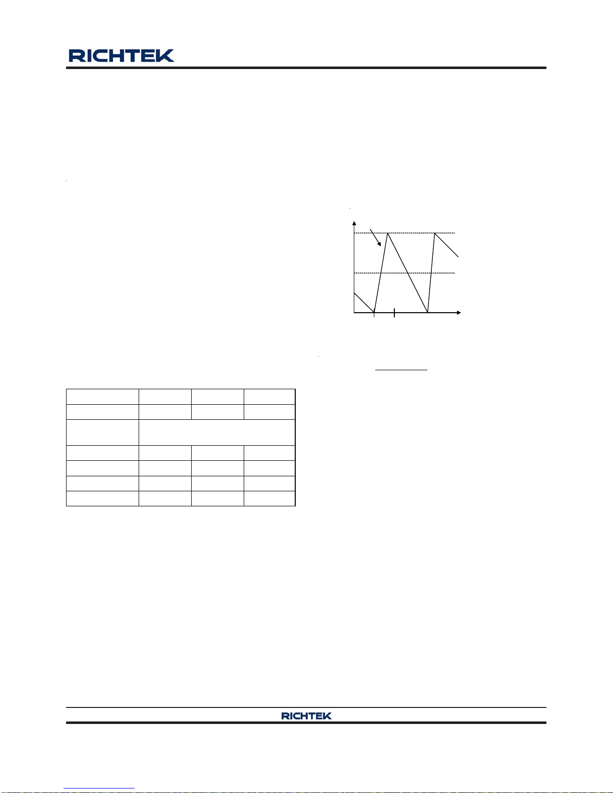
I
L
t
0
t
ON
Slope = (VIN-V
OUT
)/L
I
PEAK
I
LOAD = IPEAK
/2
Figure 3. Boundary condition of CCM/DEM
IN OUT
LOAD(SKIP) ON
(V V )
It
2L
−
≈×
where tON is the on-time.
The switching waveforms may appear noisy and
asynchronous when light loading causes diode emulation
operation. This is normal and results in high efficiency.
Trade offs in PFM noise vs. light load efficiency is made
by varying the inductor value. Generally, low inductor values
produce a broader efficiency vs. load curve, while higher
values result in higher full load efficiency (assuming that
the coil resistance remains fixed) and less output voltage
ripple. Penalties for using higher inductor values include
larger physical size and degraded load transient response
(especially at low input voltage levels).
Ultrasonic Mode
The RT8239A/B/C activates a unique type of Diode
Emulation Mode with a minimum switching frequency of
25kHz, called Ultrasonic Mode. This mode eliminates
audio-frequency modulation that would otherwise be
present when a lightly loaded controller automatically
skips pulses. In Ultrasonic Mode, the low side switch gate
driver signal is “OR”ed with an internal oscillator
(>25kHz). Once the internal oscillator is triggered, the
as one or both dead times. It occurs only in PWM mode
when the inductor current reverses at light or negative
load currents. With reversed inductor current, the
inductor's EMF causes PHASEx to go high earlier than
normal, hence extending the on-time by a period equal to
the low to high dead time. For loads above the critical
conduction point, the actual switching frequency is :
Diode Emulation Mode
In Diode Emulation Mode, the RT8239A/B automatically
reduces switching frequency at light load conditions to
maintain high efficiency. This reduction of frequency is
achieved smoothly. As the output current decreases from
heavy-load condition, the inductor current is also reduced,
and eventually comes to the point that its current valley
touches zero, which is the boundary between continuous
conduction and discontinuous conduction modes. By
emulating the behavior of diodes, the low side MOSFET
allows only partial negative current to flow when the
inductor free wheeling current becomes negative. As the
Part Number RT8239A RT8239B RT8239C
Pin Name ENM SECFB SECFB
Pin-13
Voltage Range
Mode State
4.5V to 5V ASM ASM ASM
2.3V to 3.6V DEM DEM ASM
1.2V to 1.8V ASM ASM ASM
Below 0.8V Shutdown UVP UVP
Table 1. Operation Mode Setting
load current is further decreased, it takes longer and longer
time to discharge the output capacitor to the level that
requires the next “ON” cycle. The on-time is kept the
same as that in the heavy load condition. In reverse, when
the output current increases from light load to heavy load,
the switching frequency increases to the preset value as
the inductor current reaches the continuous conduction.
The transition load point to the light load operation is shown
in Figure 3. and can be calculated as follows :
Page 18
RT8239A/B/C
18
DS8239A/B/C-06 October 2012www.richtek.com
©
Copyright 2012 Richtek Technology Corporation. All rights reserved. is a registered trademark of Richtek Technology Corporation.
I
L
t
I
PEAK
I
LOAD
I
LIMIT
Figure 4. “Valley” Current Limit
The RT8239A/B/C uses the on resistance of the
synchronous rectifier as the current sense element and
supports temperature compensated MOSFET R
DS(ON)
sensing. The R
ILIM
resistor between the ENTRIPx pin and
ultrasonic controller pulls LGATEx high and turns on the
low side MOSFET to induce a negative inductor current.
After the output voltage falls below the reference voltage,
the controller turns off the low side MOSFET (LGATEx
pulled low) and triggers a constant on-time (UGATEx driven
high). When the on-time has expired, the controller re-
enables the low side MOSFET until the controller detects
that the inductor current dropped below the zero crossing
threshold.
Linear Regulators (LDOx)
The RT8239A/B/C includes 5V (LDO5) and 3.3V (LDO3)
linear regulators. The regulators can supply up to 100mA
for external loads. Bypass LDOx with a minimum 4.7μF
ceramic capacitor. When V
OUT1
is higher than the switch
over threshold (4.66V), an internal 1.5Ω P-MOSFET switch
connects BYP1 to the LDO5 pin while simultaneously
disconnects the internal linear regulator.
Current Limit Setting (ENTRIPx)
The RT8239A/B/C has cycle-by-cycle current limit control.
The current limit circuit employs a unique “valley” current
sensing algorithm. If the magnitude of the current sense
signal at PHASEx is above the current limit threshold,
the PWM is not allowed to initiate a new cycle (Figure 4).
The actual peak current is greater than the current limit
threshold by an amount equal to the inductor ripple current.
Therefore, the exact current limit characteristic and
maximum load capability are a function of the sense
resistance, inductor value, and battery and output voltage.
GND sets the current limit threshold. The resistor, R
ILIM
,
is connected to a current source from ENTRIPx which is
10μA (typ.) at room temperature. The current source has
a 4700ppm/°C temperature slope to compensate the
temperature dependency of the R
DS(ON)
. When the voltage
drop across the sense resistor or low side MOSFET
equals 1/10 the voltage across the R
ILIM
resistor, positive
current limit will be activated. The high side MOSFET will
not be turned on until the voltage drop across the MOSFET
falls below 1/10 the voltage across the R
ILIM
resistor.
Choose a current limit resistor according to the following
equation :
V
ILIM
= (R
ILIM
x 10μA) / 10 = I
ILIM
x R
DS(ON)
R
ILIM
= (I
ILIM
x R
DS(ON)
) x 10 / 10μA
Carefully observe the PC board layout guidelines to ensure
that noise and DC errors do not corrupt the current sense
signal at PHASEx and GND. Mount or place the IC close
to the low side MOSFET.
Charge Pump (SECFB)
The external 14V charge pump is driven by LGATEx. When
LGATEx is low, C1 will be charged by V
OUT1
through D1.
C1 voltage is equal to V
OUT1
minus the diode drop. When
LGATEx becomes high, C1 transfers the charge to C2
through D2 and charges C2 voltage to V
LGATEX
plus C1
voltage. As LGATEx transitions low on the next cycle, C3
is charged to C2 voltage minus a diode drop through D3.
Finally, C3 charges C4 through D4 when LGATEx switches
high. Thus, the total charge pump voltage, VCP, is :
V
CP
= V
OUT1
+ 2 x V
LGATEx
− 4 x V
D
where V
LGATEx
is the peak voltage of the LGATEx driver
which is equal to LDO5 and VD is the forward voltage
dropped across the Schottky diode.
The SECFB pin in the RT8239B/C is used to monitor the
charge pump via a resistive voltage divider to generate
approximately 14V DC voltage and the clock driver uses
V
OUT1
as its power supply. In the event where SECFB
drops below its feedback threshold, an ultrasonic pulse
will occur to refresh the charge pump driven by LGATEx.
If there's an overload on the charge pump in which SECFB
can not reach more than its feedback threshold, the
Page 19

RT8239A/B/C
19
DS8239A/B/C-06 October 2012 www.richtek.com
©
Copyright 2012 Richtek Technology Corporation. All rights reserved. is a registered trademark of Richtek Technology Corporation.
Figure 5. Charge pump circuit connected to SECFB
MOSFET Gate Driver (UGATEx, LGA TEx)
The high side driver is designed to drive high current, low
R
DS(ON)
N-MOSFET(s). When configured as a floating driver,
5V bias voltage is delivered from the LDO5 supply. The
average drive current is also calculated by the gate charge
at VGS = 5V times switching frequency. The instantaneous
drive current is supplied by the flying capacitor between
BOOTx and PHASEx pins. A dead time to prevent shoot
through is internally generated from high side MOSFET
off to low side MOSFET on and low side MOSFET off to
high side MOSFET on.
The low side driver is designed to drive high current low
R
DS(ON)
N-MOSFET(s). The internal pull down transistor
that drives LGATEx low is robust, with a 1.5Ω typical on-
resistance. A 5V bias voltage is delivered from the LDO5
supply. The instantaneous drive current is supplied by an
input capacitor connected between LDO5 and GND.
For high current applications, some combinations of high
and low side MOSFETs may cause excessive gate drain
coupling, which leads to efficiency killing, EMI producing,
shoot through currents. This is often remedied by adding
a resistor in series with BOOTx, which increases the turn
on time of the high side MOSFET without degrading the
turn-off time. See Figure 6.
Figure 6. Increasing the UGATEx Rise Time
Soft-Start
The RT8239A/B/C provides an internal soft-start function
to prevent large inrush current and output voltage overshoot
when the converter starts up. The soft-start (SS)
automatically begins once the chip is enabled. During soft-
start, the internal current limit circuit gradually ramps up
the inductor current from zero. The maximum current limit
value is set externally as described in previous section.
The soft-start time is determined by the current limit level
and output capacitor value. The current limit threshold ramp
up time is typically 2ms from zero to 200mV after
ENTRIPx is enabled. A unique PWM duty limit control
that prevents output over voltage during soft-start period
is designed specifically for FBx floating.
UVLO Protection
The RT8239A/B/C has LDO5 under voltage lock out
protection (UVLO). When the LDO5 voltage is lower than
4.05V (typ.) and the LDO3 voltage is lower than 2.2V (typ.),
both switch power supplies are shut off. This is a non-
latch protection.
Power Good Output (PGOOD)
PGOOD is an open-drain type output and requires a pull
up resistor. PGOOD is actively held low in soft-start,
standby, and shutdown. It is released when both output
voltages are above 90% of the nominal regulation point
for RT8239A. For RT8239B/C, besides requiring both
output voltages to be above 90% of nominal regulation
point, the SECFB threshold must also be above 50% of
nominal regulation point in order for PGOOD to be released.
The PGOOD signal goes low if either output turns off or is
10% below its nominal regulation point.
SECFB
LGATE1
VOUT1
D1 D2 D3C3D4
C1
C2
C
F
R
CP1
C4
R
CP2
Charge Pump
BOOTx
R
BOOT
UGATEx
V
IN
PHASEx
controller will enter Ultrasonic Mode. Special care should
be taken to ensure that enough normal ripple voltage is
present on each cycle to prevent charge pump shutdown.
The robustness of the charge pump can be increased by
reducing the charge pump decoupling capacitor and placing
a small ceramic capacitor, CF (47pF to 220pF), in parallel
with the upper leg of the SECFB resistor feedback network,
R
CP1
, as shown below in Figure 5.
Page 20

RT8239A/B/C
20
DS8239A/B/C-06 October 2012www.richtek.com
©
Copyright 2012 Richtek Technology Corporation. All rights reserved. is a registered trademark of Richtek Technology Corporation.
Output Over Voltage Protection (OVP)
The output voltage can be continuously monitored for over
voltage. If the output voltage exceeds 12% of its set voltage
threshold, the over voltage protection is triggered and the
LGATEx low side gate drivers are forced high. This
activates the low side MOSFET switch, which rapidly
discharges the output capacitor and pulls the input voltage
downward.
The RT8239A/B/C is latched once OVP is triggered and
can only be released by either toggling ENLDO, ENTRIPx
or cycling VIN. There is a 5μs delay built into the over
voltage protection circuit to prevent false transition.
Note that latching LGATEx high will cause the output
voltage to dip slightly negative due to previously stored
energy in the LC tank circuit. For loads that cannot tolerate
a negative voltage, place a power Schottky diode across
the output to act as a reverse polarity clamp.
If the over voltage condition is caused by a short in high
side switch, turning the low side MOSFET on 100% will
create an electrical short between the battery and GND,
hence blowing the fuse and disconnecting the battery from
the output.
Output Under Voltage Protection (UVP)
The output voltage can be continuously monitored for under
voltage. If the output is less than 58% of its set voltage
threshold, the under voltage protection will be triggered
and then both UGATEx and LGATEx gate drivers will be
forced low. The UVP is ignored for at least 5ms (typ.)
after a start up or a rising edge on ENTRIPx. Toggle
ENTRIPx or cycle VIN to reset the UVP fault latch and
restart the controller.
Thermal Protection
The RT8239A/B/C features thermal shutdown to prevent
damage from excessive heat dissipation. Thermal
shutdown occurs when the die temperature exceeds
150°C. All internal circuitry is inactive during thermal
shutdown. The RT8239A/B/C triggers thermal shutdown
if LDOx is not supplied from V
OUTx
, while input voltage on
VIN and drawing current from LDOx are too high.
Nevertheless, even if LDOx is supplied from V
OUTx
,
overloading LDOx can cause large power dissipation on
automatic switches, which may still result in thermal
shutdown.
Discharge Mode (Soft Discharge)
When ENTRIPx is low and a transition to standby or
shutdown mode occurs, or the output under voltage fault
latch is set, the output discharge mode will be triggered.
During discharge mode, an internal switch creates a path
for discharging the output capacitors' residual charge to
GND.
Shutdown Mode
SMPS1, SMPS2, LDO3 and LDO5 all have independent
enabling control. Drive ENLDO, ENTRIP1 and ENTRIP2
below the precise input falling edge trip level to place the
RT8239A/B/C in its low power shutdown state. The
RT8239A/B/C consumes only 20μA of input current while
in shutdown. When shutdown mode is activated, the
reference turns off. The accurate 0.95V falling edge
threshold on ENLDO can be used to detect a specific
analog voltage level and to shutdown the device. Once in
shutdown, the 1.6V rising edge threshold activates,
providing sufficient hysteresis for most applications.
Power Up Sequencing and On/Off Controls
(ENTRIPx, ENM)
ENTRIP1 and ENTRIP2 control SMPS power up
sequencing. When the RT8239A/B/C is applied in the
single channel mode, ENTRIPx disables the respective
output when ENTRIPx voltage rises above 4.5V.
Furthermore, when the RT8239A is applied in the dual
channel mode, the outputs are enabled when ENM voltage
rises above 2.3V.
Page 21

RT8239A/B/C
21
DS8239A/B/C-06 October 2012 www.richtek.com
©
Copyright 2012 Richtek Technology Corporation. All rights reserved. is a registered trademark of Richtek Technology Corporation.
Table1. Operation Mode Truth Table
Mode Condition Comment
Power Up LDOx
< UVLO threshold
Transitions to discharge mode after VIN POR and
after REF becomes valid. LDO5 and LDO3 remain
active.
Run
ENLDO = high, V
OUT1
or V
OUT2
are
enabled
Normal Operation.
Over Voltage
Protection
Either output > 112% of the nominal level.
LGATEx is forced high. LDO3 and LDO5 are active.
Exit by VIN POR or by toggling ENLDO, ENTRIPx,
and ENM.
Under Voltage
Protection
Either output < 58% of the nominal level
after 3ms time-out expires and output is
enabled
Both UGATEx and LGATEx are forced low and
enter discharge mode. LDO3 and LDO5 are active.
Exit by VIN POR or by toggling ENLDO, ENTRIPx,
and ENM.
Discharge
Either output is still high in standby mode
or shutdown mode
During discharge mode, there is one path to
discharge the output capacitors’ residual charge to
GND via an internal switch.
Standby
ENTRIPx or ENM < startup threshold,
ENLDO = high.
LDO3 and LDO5 are active.
Shutdown ENLDO = low All circuitry are off.
Thermal
Shutdown
T
J
> 150°C
All circuitry are off. Exit by VIN POR or by toggling
ENLDO, ENTRIPx, and ENM.
Table 2. Power up Sequencing (RT8239A)
ENLDO (V) ENM (V)
ENTRIP1
(V)
ENTRIP2
(V)
LDO5 LDO3 SMPS1 SMPS2
Low Low X X Off Off Off Off
“>1.6V”
=> High
Low X X On On Off Off
“>1.6V”
=> High
“>2.3V”
=> High
Off Off On On Off Off
“>1.6V”
=> High
“>2.3V”
=> High
Off On On On Off On
“>1.6V”
=> High
“>2.3V”
=> High
On On On On On On
“>1.6V”
=> High
“>2.3V”
=> High
On Off On On On Off
Page 22

RT8239A/B/C
22
DS8239A/B/C-06 October 2012www.richtek.com
©
Copyright 2012 Richtek Technology Corporation. All rights reserved. is a registered trademark of Richtek Technology Corporation.
Output Voltage Setting (FBx)
Connect a resistive voltage divider at the FBx pin between
V
OUTx
and GND to adjust the output voltage between 2V
and 5.5V (Figure 7). Choose R2 to be approximately 10kΩ,
and solve for R1 using the equation :
⎛⎞
⎛⎞
=×+
⎜⎟
⎜⎟
⎝⎠
⎝⎠
OUT FBx
R1
VV1
R2
where V
FBx
is 2V (typ.).
UGATEx
PHASEx
LGATEx
PGND
FBx
GND
R1
R2
VOUTx
V
IN
Figure 7. Setting V
OUTx
with a resistive voltage divider
Output Inductor Selection
The switching frequency (on-time) and operating point (%
ripple or LIR) determine the inductor value as shown
below :
×−
=
×
ON IN OUTx
LOAD(MAX)
t(VV)
L
LIR I
where LIR is the ratio of the peak-to-peak ripple current to
the average inductor current.
Find a low-loss inductor having the lowest possible DC
resistance that fits in the allotted dimensions. Ferrite cores
are often the best choice, although powdered iron is
inexpensive and can work well at 200kHz. The core must
be large enough not to saturate at the peak inductor
current, I
PEAK
:
I
PEAK
= I
LOAD(MAX)
+ [ (LIR / 2) x I
LOAD(MAX)
]
The calculation above shall serve as a general reference.
To further improve transient response, the output
inductance can be further reduced. Of course, besides
the inductor, the output capacitor should also be
considered when improving transient response.
Output Capacitor Selection
The capacitor value and ESR determine the amount of
output voltage ripple and load transient response. Thus,
the capacitor value must be greater than the largest value
calculated from below equations.
Δ××+
=
⎡⎤
×××−
⎣⎦
2
LOAD ON OFF(MIN)
SAG
OUT IN ON OUTx ON OFF(MIN)
(I ) L (t t )
V
2C V t V (t + t )
()
2
LOAD
SOAR
OUT OUTx
IL
V
2C V
Δ×
=
××
−
⎛⎞
=× ×
⎜⎟
××
⎝⎠
P P LOAD(MAX)
OUT
1
V LIR I ESR +
8C f
where V
SAG
and V
SOAR
are the allowable amount of
undershoot and overshoot voltage during load transient,
V
p-p
is the output ripple voltage, and t
OFF(MIN)
is the
minimum off-time.
Thermal Considerations
For continuous operation, do not exceed absolute
maximum junction temperature. The maximum power
dissipation depends on the thermal resistance of the IC
package, PCB layout, rate of surrounding airflow, and
difference between junction and ambient temperature. The
maximum power dissipation can be calculated by the
following formula :
P
D(MAX)
= (T
J(MAX)
− TA) / θ
JA
where T
J(MAX)
is the maximum junction temperature, TA is
the ambient temperature, and θ
JA
is the junction to ambient
thermal resistance.
For recommended operating condition specifications, the
maximum junction temperature is 125°C. The junction to
ambient thermal resistance, θJA, is layout dependent. For
WQFN-20L 3x3 packages, the thermal resistance, θJA, is
30°C/W on a standard JEDEC 51-7 four-layer thermal test
board. The maximum power dissipation at TA = 25°C can
be calculated by the following formula :
P
D(MAX)
= (125°C − 25°C) / (30°C/W) = 3.33W for
WQFN-20L 3x3 package
The maximum power dissipation depends on the operating
ambient temperature for fixed T
J(MAX)
and thermal
Page 23

©
Copyright 2012 Richtek Technology Corporation. All rights reserved. is a registered trademark of Richtek Technology Corporation.
RT8239A/B/C
23
DS8239A/B/C-06 October 2012 www.richtek.com
©
Copyright 2012 Richtek Technology Corporation. All rights reserved. is a registered trademark of Richtek Technology Corporation.
resistance, θJA. The derating curve in Figure 8 allows the
designer to see the effect of rising ambient temperature
on the maximum power dissipation.
Figure 8. Derating Curve of Maximum Power Dissipation
Layout Considerations
Layout is very important in high frequency switching
converter design. Improper PCB layout can radiate
excessive noise and contribute to the converter’s
instability. Certain points must be considered before
starting a layout with the RT8239A/B/C.
` Place the filter capacitor close to the IC, within 12mm
(0.5 inch) if possible.
` Keep current limit setting network as close as possible
to the IC. Routing of the network should avoid coupling
to high-voltage switching node.
` Connections from the drivers to the respective gate of
the high side or the low side MOSFET should be as
short as possible to reduce stray inductance. Use
0.65mm (25 mils) or wider trace.
` All sensitive analog traces and components such as
FBx, ENTRIPx, PGOOD, and TON should be placed
away from high voltage switching nodes such as
PHASEx, LGATEx, UGATEx, or BOOTx nodes to avoid
coupling. Use internal layer(s) as ground plane(s) and
shield the feedback trace from power traces and
components.
` Place ground terminal of VIN capacitor(s), V
OUTx
capacitor(s), and source of low side MOSFETs as close
to each other as possible. The PCB trace of PHASEx
node, which connects to source of high side MOSFET,
drain of low side MOSFET and high voltage side of the
inductor, should be as short and wide as possible.
0.0
0.6
1.2
1.8
2.4
3.0
3.6
0 25 50 75 100 125
Ambient Temperature (°C)
Maximum Power Dissipation (W) 1
Four-Layer PCB
Page 24

RT8239A/B/C
24
DS8239A/B/C-06 October 2012www.richtek.com
Richtek Technology Corporation
5F, No. 20, Taiyuen Street, Chupei City
Hsinchu, Taiwan, R.O.C.
Tel: (8863)5526789
Richtek products are sold by description only. Richtek reserves the right to change the circuitry and/or specifications without notice at any time. Customers should
obtain the latest relevant information and data sheets before placing orders and should verify that such information is current and complete. Richtek cannot
assume responsibility for use of any circuitry other than circuitry entirely embodied in a Richtek product. Information furnished by Richtek is believed to be
accurate and reliable. However, no responsibility is assumed by Richtek or its subsidiaries for its use; nor for any infringements of patents or other rights of third
parties which may result from its use. No license is granted by implication or otherwise under any patent or patent rights of Richtek or its subsidiaries.
Outline Dimension
Dimensions In Millimeters Dimensions In Inches
Symbol
Min Max Min Max
A 0.700 0.800 0.028 0.031
A1 0.000 0.050 0.000 0.002
A3 0.175 0.250 0.007 0.010
b 0.150 0.250 0.006 0.010
D 2.900 3.100 0.114 0.122
D2 1.650 1.750 0.065 0.069
E 2.900 3.100 0.114 0.122
E2 1.650 1.750 0.065 0.069
e 0.400 0.016
L 0.350 0.450
0.014 0.018
W-Type 20L QFN 3x3 Package
Note : The configuration of the Pin #1 identifier is optional,
but must be located within the zone indicated.
DETAIL A
Pin #1 ID and Tie Bar Mark Options
1
1
2
2
 Loading...