

Page 1

RT8168B
Dual Single-Phase PWM Controller for CPU and GPU Core
Power Supply
General Description
The RT8168B is a dual single-pha se PWM controller with
integrated MOSFET drivers, compliant with Intel IMVP7
Pulse Width Modulation Specification to support both
CPU core and GPU core power. This part a dopts G-NA VP
(Green-Native A VP), which is a Richtek proprietary topology
derived from finite DC gain compen sator in consta nt ontime control mode. G-NAVPTM makes this part an easy
setting PWM controller to meet all Intel AVP (Active
V oltage Positioning) mobile CPU/GPU requirements. The
RT8168B uses SVID interface to control a n 8-bit DAC for
output voltage programming. The built-in high accuracy
DAC converts the received VID code into a voltage value
ranging from 0V to 1.52V with 5mV step voltage. The
system accuracy of the controller can reach 0.8%. The
RT8168B operates in continuous conduction mode or
diode emulation mode, according to the SVID command.
The maximum efficiency ca n reach up to 90% in dif ferent
operating modes according to different load conditions.
The droop function (load line) can be ea sily progra mmed
by setting the DC gain of the error amplifier. With proper
compensation, the load transient response can achieve
optimized A VP performance.
The output voltage transition slew rate is set vi a the SVID
interface. The RT8168B supports both DCR and sense
resistor current sensing. The RT8168B provides
VR_READY and thermal throttling output signals for
IMVP7 CPU and GPU core. This part also features
complete fault protection functions including over voltage,
under voltage, negative voltage, over current and thermal
shutdown.
TM
Features
zz
z Dual Single-Phase PWM Controller for CPU Core
zz
and GPU Core Power
zz
z IMVP7 Compatible Power Management States
zz
zz
z Serial VID Interface
zz
zz
z G-NAV P
zz
zz
z A V P f or CPU VR Only
zz
zz
z 0.5% DAC Accuracy
zz
zz
z 0.8% System Accuracy
zz
zz
z Differential Remote Voltage Sensing
zz
zz
z Built-in ADC for Platform Programming
zz
` SETINI/SETINIA for CPU/GPU Core VR Initial
TM
T opology
Startup Voltage
` TMPMAX to Set Platform Maximum Temperature
` ICCMAX/ICCMAXA for CPU/GPU Core VR
Maximum Current
zz
z Power Good Indicator : VR_READY/VRA_READY for
zz
CPU/GPU Core Power
zz
z Thermal Throttling Indicator : VRHOT
zz
zz
z Diode Emulation Mode at Light Load Condition
zz
zz
z Fast Line/Load Transient Response
zz
zz
z Switching Frequency up to 1MHz per Phase
zz
zz
z OVP, UVP, NVP, OTP, UVLO, OCP
zz
zz
z Small 40-Lead WQFN Package
zz
zz
z RoHS Compliant and Halogen Free
zz
Applications
z IMVP7 Intel CPU/GPU Core Power Supply
z Laptop Computers
z A VP Step-Down Converter
The RT8168B is available in a WQFN-40L 5x5 small
footprint pack age.
DS8168B-00 November 2011 www.richtek.com
1
Page 2
RT8168B
Ordering Information
RT8168B
Package Type
QW : WQFN-40L 5x5 (W-Type)
Lead Plating System
G : Green (Halogen Free and Pb Free)
Note :
Richtek products are :
` RoHS compliant and compatible with the current require-
ments of IPC/JEDEC J-STD-020.
` Suitable for use in SnPb or Pb-free soldering processes.
Marking Information
RT8168BGQW : Product Number
RT8168B
GQW
YMDNN
YMDNN : Date Code
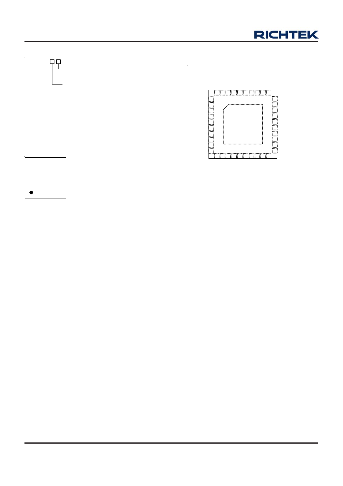
Pin Configurations
(TOP VIEW)
UGATE1
PHASE1
LGATE1
PVCC
LGATEA
PHASEA
FB
VCC
10
1
2
3
4
5
6
7
8
9
SETINI
ICCMAX
TMPMAX
ICCMAXA
WQFN-40L 5x5
GND
TSEN
OCSET
BOOT1
TONSET
ISEN1P
ISEN1N
COMP
RGND
GFXPS2
SETINIA
UGATEA
BOOTAENTONSETA
41
TSENA
OCSETA
31323334353637383940
20191817161514131211
IBIAS
VRHOT
30
ISENAP
29
ISENAN
28
COMPA
27
FBA
26
RGNDA
25
VCLK
24
VDIO
23
ALERT
22
VRA_READY
21
VR_READY
DS8168B-00 November 2011www.richtek.com
2
Page 3
Typical Application Circuit
1
R
V
C
C
.
2
2
C
1
F
µ
1
8
R
R
R
1
9
0
1
R
1
k
0
1
0
5
1
5
k
7
0
1
2
2
2
2
2
2
R
R
1
8
k
.
8
7
R
2
1
9
0
k
0
1
k
0
1
1
1
1
1
R
2
5
2
R
6
R
2
N
k
0
1
R
3
0
R
k
0
1
5
7
N
C
C
3
1
R
3
2
k
0
0
N
C
1
1
1
R
3
R
8
3
9
R
4
0
k
0
k
.
6
1
1
.
k
1
5
N
T
C
T
R
4
7
1
2
k
7
R
2
7
5
0
A
1
0
k
3
=
ß
3
8
0
1
1
1
R
5
3
5
R
1
k
4
5
3
6
.
k
V
R
V
V
V
V
V
A
L
A
_
R
E
_
R
R
E
V
R
O
C
O
S
E
S
T
M
C
I
ICCMAXA
GFXPS2
C
C
V
5
P
C
C
C
L
K
D
O
I
E
R
T
A
D
Y
A
D
Y
O
H
T
V
C
S
E
T
C
S
E
T
I
N
I
N
E
T
I
V
C
P
M
A
X
C
M
A
X
R
4
1
2
R
7
6
R
0
3
1
0
3
1
C
R
1
7
k
7
2
A
T
A
I
R
2
4
k
0
1
C
R
2
9
1k1
5
R
3
7
k
3
3
6
N
T
C
T
1
1
0
k
k
=
3
ß
3
8
0
7
R
1
7
5
0
5
R
2
1
k
RT8168B
9
RT8168B
V
C
C
5
V
C
L
K
4
V
O
D
I
3
A
L
E
R
T
2
V
R
A
_
R
1
V
R
_
R
E
0
V
R
H
O
T
8
O
S
C
E
T
6
O
S
C
E
T
0
S
E
T
I
N
1
S
E
T
I
N
2
T
P
M
M
3
C
C
I
M
A
4
C
I
M
A
C
8
G
F
X
P
S
7
T
S
E
N
A
5
T
S
E
N
9
I
A
B
S
I
T
N
O
S
E
G
U
A
T
E
B
O
O
T
P
H
A
S
E
L
G
A
T
E
E
A
D
Y
P
V
A
Y
D
A
A
I
I
A
X
X
X
A
2
C
S
I
E
1
N
I
S
E
N
1
F
O
M
C
R
G
N
T
O
N
S
E
T
U
G
A
T
E
B
O
T
O
P
A
H
S
E
L
G
A
T
E
S
I
E
N
A
I
S
E
N
A
F
B
P
M
C
O
G
R
N
D
N
G
R
2
k
0
3
1
2
T
0
R
4
4
0
1
0
R
5
1
1
3
9
1
1
R
2
3
1
3
C
3
P
4
N
6
B
5
P
7
D
3
A
3
A
3
A
3
A
3
A
3
P
2
N
2
A
2
A
2
A
4
D
0
8
7
t
i
o
O
p
0
1
C
2
R
1
7
3
R
3
0
3
1
1
0
3
R
5
4
0
R
3
6
3
5
R
4
1
0
6
0
9
t
i
o
O
p
7
8
6
1
9
1
C
8
R
4
k
2
4
E
x
(
p
e
o
s
R
3
.
1
5
2
C
F
µ
.
1
0
Q
1
C
4
F
µ
.
1
0
Q
2
V
5
C
8
F
µ
1
l
a
n
1
k
k
l
a
n
d
P
l
a
n
t
i
O
p
o
1
1
C
2
2
R
k
0
1
R
3
4
1
.
5
2
1
C
F
µ
.
1
0
Q
3
C
1
3
F
µ
.
1
0
Q
4
l
a
t
p
n
i
o
O
0
2
C
9
R
4
k
0
1
a
d
)
C
0
1
a
t
i
n
o
O
p
1
R
3
7
C
3
2
R
0
0
1
C
0
1
a
t
n
i
p
o
O
4
R
2
C
1
5
0
5
R
0
0
1
3
F
µ
R
D
C
l
1
R
1
4
k
.
9
3
C
9
O
8
2
R
0
0
1
1
4
F
µ
R
C
D
2
l
R
4
3
k
1
1
8
C
1
1
5
R
0
0
1
V
N
I
5
t
V
o
2
5
V
m
.
6
=
7
L
1
H
µ
C
6
F
µ
8
.
6
0
0
R
R
.
2
a
n
t
i
p
o
O
R
C
V
CORE
1
1
6
.
7
4
k
4
l
E
S
V
E
C
C
CORE VSS SENSE
V
N
I
5
V
o
2
t
5
V
m
.
6
4
1
=
L
2
H
µ
C
1
6
F
µ
1
.
0
R
4
R
1
t
O
p
F
G
V
G
F
G
4
4
5
k
1
k
.
2
l
a
n
i
o
N
E
S
V
X
C
C
F
X
N
E
S
V
X
S
S
V
C
R
O
E
2
C
C
5
F
µ
0
3
3
m
9
/
T
N
C
5
k
7
.
4
k
3
ß
=
E
S
N
V
F
G
X
C
1
7
F
µ
0
3
3
m
5
/
1
T
N
C
A
k
1
5
6
3
ß
=
E
S
E
S
6
F
µ
0
3
3
m
/
9
1
0
0
5
C
2
7
F
µ
0
3
3
m
/
5
1
0
3
Chip Enable
2
N
E
DS8168B-00 November 2011 www.richtek.com
3
Page 4

RT8168B
Table 1. IMVP7/VR12 Compliant VID Table
VID7 VID6 VID5 VID4 VID3 VID2 VID1 VID0 H1 H0 VDAC Voltage
0 0 0 0 0 0 0 0 0 0 0.000
0 0 0 0 0 0 0 1 0 1 0.250
0 0 0 0 0 0 1 0 0 2 0.255
0 0 0 0 0 0 1 1 0 3 0.260
0 0 0 0 0 1 0 0 0 4 0.265
0 0 0 0 0 1 0 1 0 5 0.270
0 0 0 0 0 1 1 0 0 6 0.275
0 0 0 0 0 1 1 1 0 7 0.280
0 0 0 0 1 0 0 0 0 8 0.285
0 0 0 0 1 0 0 1 0 9 0.290
0 0 0 0 1 0 1 0 0 A 0.295
0 0 0 0 1 0 1 1 0 B 0.300
0 0 0 0 1 1 0 0 0 C 0.305
0 0 0 0 1 1 0 1 0 D 0.310
0 0 0 0 1 1 1 0 0 E 0.315
0 0 0 0 1 1 1 1 0 F 0.320
0 0 0 1 0 0 0 0 1 0 0.325
0 0 0 1 0 0 0 1 1 1 0.330
0 0 0 1 0 0 1 0 1 2 0.335
0 0 0 1 0 0 1 1 1 3 0.340
0 0 0 1 0 1 0 0 1 4 0.345
0 0 0 1 0 1 0 1 1 5 0.350
0 0 0 1 0 1 1 0 1 6 0.355
0 0 0 1 0 1 1 1 1 7 0.360
0 0 0 1 1 0 0 0 1 8 0.365
0 0 0 1 1 0 0 1 1 9 0.370
0 0 0 1 1 0 1 0 1 A 0.375
0 0 0 1 1 0 1 1 1 B 0.380
0 0 0 1 1 1 0 0 1 C 0.385
0 0 0 1 1 1 0 1 1 D 0.390
0 0 0 1 1 1 1 0 1 E 0.395
0 0 0 1 1 1 1 1 1 F 0.400
0 0 1 0 0 0 0 0 2 0 0.405
0 0 1 0 0 0 0 1 2 1 0.410
0 0 1 0 0 0 1 0 2 2 0.415
To be continued
DS8168B-00 November 2011www.richtek.com
4
Page 5

RT8168B
VID7 VID6 VID5 VID4 VID3 VID2 VID1 VID0 H1 H0 DAC Voltage
0 0 1 0 0 0 1 1 2 3 0.420
0 0 1 0 0 1 0 0 2 4 0.425
0 0 1 0 0 1 0 1 2 5 0.430
0 0 1 0 0 1 1 0 2 6 0.435
0 0 1 0 0 1 1 1 2 7 0.440
0 0 1 0 1 0 0 0 2 8 0.445
0 0 1 0 1 0 0 1 2 9 0.450
0 0 1 0 1 0 1 0 2 A 0.455
0 0 1 0 1 0 1 1 2 B 0.460
0 0 1 0 1 1 0 0 2 C 0.465
0 0 1 0 1 1 0 1 2 D 0.470
0 0 1 0 1 1 1 0 2 E 0.475
0 0 1 0 1 1 1 1 2 F 0.480
0 0 1 1 0 0 0 0 3 0 0.485
0 0 1 1 0 0 0 1 3 1 0.490
0 0 1 1 0 0 1 0 3 2 0.495
0 0 1 1 0 0 1 1 3 3 0.500
0 0 1 1 0 1 0 0 3 4 0.505
0 0 1 1 0 1 0 1 3 5 0.510
0 0 1 1 0 1 1 0 3 6 0.515
0 0 1 1 0 1 1 1 3 7 0.520
0 0 1 1 1 0 0 0 3 8 0.525
0 0 1 1 1 0 0 1 3 9 0.530
0 0 1 1 1 0 1 0 3 A 0.535
0 0 1 1 1 0 1 1 3 B 0.540
0 0 1 1 1 1 0 0 3 C 0.545
0 0 1 1 1 1 0 1 3 D 0.550
0 0 1 1 1 1 1 0 3 E 0.555
0 0 1 1 1 1 1 1 3 F 0.560
0 1 0 0 0 0 0 0 4 0 0.565
0 1 0 0 0 0 0 1 4 1 0.570
0 1 0 0 0 0 1 0 4 2 0.575
0 1 0 0 0 0 1 1 4 3 0.580
0 1 0 0 0 1 0 0 4 4 0.585
0 1 0 0 0 1 0 1 4 5 0.590
To be continued
DS8168B-00 November 2011 www.richtek.com
5
Page 6

RT8168B
VID7 VID6 VID5 VID4 VID3 VID2 VID1 VID0 H1 H0 DAC Voltage
0 1 0 0 0 1 1 0 4 6 0.595
0 1 0 0 0 1 1 1 4 7 0.600
0 1 0 0 1 0 0 0 4 8 0.605
0 1 0 0 1 0 0 1 4 9 0.610
0 1 0 0 1 0 1 0 4 A 0.615
0 1 0 0 1 0 1 1 4 B 0.620
0 1 0 0 1 1 0 0 4 C 0.625
0 1 0 0 1 1 0 1 4 D 0.630
0 1 0 0 1 1 1 0 4 E 0.635
0 1 0 0 1 1 1 1 4 F 0.640
0 1 0 1 0 0 0 0 5 0 0.645
0 1 0 1 0 0 0 1 5 1 0.650
0 1 0 1 0 0 1 0 5 2 0.655
0 1 0 1 0 0 1 1 5 3 0.660
0 1 0 1 0 1 0 0 5 4 0.665
0 1 0 1 0 1 0 1 5 5 0.670
0 1 0 1 0 1 1 0 5 6 0.675
0 1 0 1 0 1 1 1 5 7 0.680
0 1 0 1 1 0 0 0 5 8 0.685
0 1 0 1 1 0 0 1 5 9 0.690
0 1 0 1 1 0 1 0 5 A 0.695
0 1 0 1 1 0 1 1 5 B 0.700
0 1 0 1 1 1 0 0 5 C 0.705
0 1 0 1 1 1 0 1 5 D 0.710
0 1 0 1 1 1 1 0 5 E 0.715
0 1 0 1 1 1 1 1 5 F 0.720
0 1 1 0 0 0 0 0 6 0 0.725
0 1 1 0 0 0 0 1 6 1 0.730
0 1 1 0 0 0 1 0 6 2 0.735
0 1 1 0 0 0 1 1 6 3 0.740
0 1 1 0 0 1 0 0 6 4 0.745
0 1 1 0 0 1 0 1 6 5 0.750
0 1 1 0 0 1 1 0 6 6 0.755
0 1 1 0 0 1 1 1 6 7 0.760
0 1 1 0 1 0 0 0 6 8 0.765
0 1 1 0 1 0 0 1 6 9 0.770
DS8168B-00 November 2011www.richtek.com
6
To be continued
Page 7

RT8168B
VID7 VID6 VID5 VID4 VID3 VID2 VID1 VID0 H1 H0 DAC Voltage
0 1 1 0 1 0 1 0 6 A 0.775
0 1 1 0 1 0 1 1 6 B 0.780
0 1 1 0 1 1 0 0 6 C 0.785
0 1 1 0 1 1 0 1 6 D 0.790
0 1 1 0 1 1 1 0 6 E 0.795
0 1 1 0 1 1 1 1 6 F 0.800
0 1 1 1 0 0 0 0 7 0 0.805
0 1 1 1 0 0 0 1 7 1 0.810
0 1 1 1 0 0 1 0 7 2 0.815
0 1 1 1 0 0 1 1 7 3 0.820
0 1 1 1 0 1 0 0 7 4 0.825
0 1 1 1 0 1 0 1 7 5 0.830
0 1 1 1 0 1 1 0 7 6 0.835
0 1 1 1 0 1 1 1 7 7 0.840
0 1 1 1 1 0 0 0 7 8 0.845
0 1 1 1 1 0 0 1 7 9 0.850
0 1 1 1 1 0 1 0 7 A 0.855
0 1 1 1 1 0 1 1 7 B 0.860
0 1 1 1 1 1 0 0 7 C 0.865
0 1 1 1 1 1 0 1 7 D 0.870
0 1 1 1 1 1 1 0 7 E 0.875
0 1 1 1 1 1 1 1 7 F 0.880
1 0 0 0 0 0 0 0 8 0 0.885
1 0 0 0 0 0 0 1 8 1 0.890
1 0 0 0 0 0 1 0 8 2 0.895
1 0 0 0 0 0 1 1 8 3 0.900
1 0 0 0 0 1 0 0 8 4 0.905
1 0 0 0 0 1 0 1 8 5 0.910
1 0 0 0 0 1 1 0 8 6 0.915
1 0 0 0 0 1 1 1 8 7 0.920
1 0 0 0 1 0 0 0 8 8 0.925
1 0 0 0 1 0 0 1 8 9 0.930
1 0 0 0 1 0 1 0 8 A 0.935
1 0 0 0 1 0 1 1 8 B 0.940
1 0 0 0 1 1 0 0 8 C 0.945
1 0 0 0 1 1 0 1 8 D 0.950
DS8168B-00 November 2011 www.richtek.com
To be continued
7
Page 8

RT8168B
VID7 VID6 VID5 VID4 VID3 VID2 VID1 VID0 H1 H0 DAC Voltage
1 0 0 0 1 1 1 0 8 E 0.955
1 0 0 0 1 1 1 1 8 F 0.960
1 0 0 1 0 0 0 0 9 0 0.965
1 0 0 1 0 0 0 1 9 1 0.970
1 0 0 1 0 0 1 0 9 2 0.975
1 0 0 1 0 0 1 1 9 3 0.980
1 0 0 1 0 1 0 0 9 4 0.985
1 0 0 1 0 1 0 1 9 5 0.990
1 0 0 1 0 1 1 0 9 6 0.995
1 0 0 1 0 1 1 1 9 7 1.000
1 0 0 1 1 0 0 0 9 8 1.005
1 0 0 1 1 0 0 1 9 9 1.010
1 0 0 1 1 0 1 0 9 A 1.015
1 0 0 1 1 0 1 1 9 B 1.020
1 0 0 1 1 1 0 0 9 C 1.025
1 0 0 1 1 1 0 1 9 D 1.030
1 0 0 1 1 1 1 0 9 E 1.035
1 0 0 1 1 1 1 1 9 F 1.040
1 0 1 0 0 0 0 0 A 0 1.045
1 0 1 0 0 0 0 1 A 1 1.050
1 0 1 0 0 0 1 0 A 2 1.055
1 0 1 0 0 0 1 1 A 3 1.060
1 0 1 0 0 1 0 0 A 4 1.065
1 0 1 0 0 1 0 1 A 5 1.070
1 0 1 0 0 1 1 0 A 6 1.075
1 0 1 0 0 1 1 1 A 7 1.080
1 0 1 0 1 0 0 0 A 8 1.085
1 0 1 0 1 0 0 1 A 9 1.090
1 0 1 0 1 0 1 0 A A 1.095
1 0 1 0 1 0 1 1 A B 1.100
1 0 1 0 1 1 0 0 A C 1.105
1 0 1 0 1 1 0 1 A D 1.110
1 0 1 0 1 1 1 0 A E 1.115
1 0 1 0 1 1 1 1 A F 1.120
1 0 1 1 0 0 0 0 B 0 1.125
1 0 1 1 0 0 0 1 B 1 1.130
To be continued
DS8168B-00 November 2011www.richtek.com
8
Page 9

RT8168B
VID7 VID6 VID5 VID4 VID3 VID2 VID1 VID0 H1 H0 DAC Voltage
1 0 1 1 0 0 1 0 B 2 1.135
1 0 1 1 0 0 1 1 B 3 1.140
1 0 1 1 0 1 0 0 B 4 1.145
1 0 1 1 0 1 0 1 B 5 1.150
1 0 1 1 0 1 1 0 B 6 1.155
1 0 1 1 0 1 1 1 B 7 1.160
1 0 1 1 1 0 0 0 B 8 1.165
1 0 1 1 1 0 0 1 B 9 1.170
1 0 1 1 1 0 1 0 B A 1.175
1 0 1 1 1 0 1 1 B B 1.180
1 0 1 1 1 1 0 0 B C 1.185
1 0 1 1 1 1 0 1 B D 1.190
1 0 1 1 1 1 1 0 B E 1.195
1 0 1 1 1 1 1 1 B F 1.200
1 1 0 0 0 0 0 0 C 0 1.205
1 1 0 0 0 0 0 1 C 1 1.210
1 1 0 0 0 0 1 0 C 2 1.215
1 1 0 0 0 0 1 1 C 3 1.220
1 1 0 0 0 1 0 0 C 4 1.225
1 1 0 0 0 1 0 1 C 5 1.230
1 1 0 0 0 1 1 0 C 6 1.235
1 1 0 0 0 1 1 1 C 7 1.240
1 1 0 0 1 0 0 0 C 8 1.245
1 1 0 0 1 0 0 1 C 9 1.250
1 1 0 0 1 0 1 0 C A 1.255
1 1 0 0 1 0 1 1 C B 1.260
1 1 0 0 1 1 0 0 C C 1.265
1 1 0 0 1 1 0 1 C D 1.270
1 1 0 0 1 1 1 0 C E 1.275
1 1 0 0 1 1 1 1 C F 1.280
1 1 0 1 0 0 0 0 D 0 1.285
1 1 0 1 0 0 0 1 D 1 1.290
1 1 0 1 0 0 1 0 D 2 1.295
1 1 0 1 0 0 1 1 D 3 1.300
1 1 0 1 0 1 0 0 D 4 1.305
1 1 0 1 0 1 0 1 D 5 1.310
DS8168B-00 November 2011 www.richtek.com
To be continued
9
Page 10

RT8168B
VID7 VID6 VID5 VID4 VID3 VID2 VID1 VID0 H1 H0 DAC Voltage
1 1 0 1 0 1 1 0 D 6 1.315
1 1 0 1 0 1 1 1 D 7 1.320
1 1 0 1 1 0 0 0 D 8 1.325
1 1 0 1 1 0 0 1 D 9 1.330
1 1 0 1 1 0 1 0 D A 1.335
1 1 0 1 1 0 1 1 D B 1.340
1 1 0 1 1 1 0 0 D C 1.345
1 1 0 1 1 1 0 1 D D 1.350
1 1 0 1 1 1 1 0 D E 1.355
1 1 0 1 1 1 1 1 D F 1.360
1 1 1 0 0 0 0 0 E 0 1.365
1 1 1 0 0 0 0 1 E 1 1.370
1 1 1 0 0 0 1 0 E 2 1.375
1 1 1 0 0 0 1 1 E 3 1.380
1 1 1 0 0 1 0 0 E 4 1.385
1 1 1 0 0 1 0 1 E 5 1.390
1 1 1 0 0 1 1 0 E 6 1.395
1 1 1 0 0 1 1 1 E 7 1.400
1 1 1 0 1 0 0 0 E 8 1.405
1 1 1 0 1 0 0 1 E 9 1.410
1 1 1 0 1 0 1 0 E A 1.415
1 1 1 0 1 0 1 1 E B 1.420
1 1 1 0 1 1 0 0 E C 1.425
1 1 1 0 1 1 0 1 E D 1.430
1 1 1 0 1 1 1 0 E E 1.435
1 1 1 0 1 1 1 1 E F 1.440
1 1 1 1 0 0 0 0 F 0 1.445
1 1 1 1 0 0 0 1 F 1 1.450
1 1 1 1 0 0 1 0 F 2 1.455
1 1 1 1 0 0 1 1 F 3 1.460
1 1 1 1 0 1 0 0 F 4 1.465
1 1 1 1 0 1 0 1 F 5 1.470
1 1 1 1 0 1 1 0 F 6 1.475
1 1 1 1 0 1 1 1 F 7 1.480
1 1 1 1 1 0 0 0 F 8 1.485
To be continued
DS8168B-00 November 2011www.richtek.com
10
Page 11

RT8168B
VID7 VID6 VID5 VID4 VID3 VID2 VID1 VID0 H1 H0 DAC Voltage
1 1 1 1 1 0 0 1 F 9 1.490
1 1 1 1 1 0 1 0 F A 1.495
1 1 1 1 1 0 1 1 F B 1.500
1 1 1 1 1 1 0 0 F C 1.505
1 1 1 1 1 1 0 1 F D 1.510
1 1 1 1 1 1 1 0 F E 1.515
1 1 1 1 1 1 1 1 F F 1.520
DS8168B-00 November 2011 www.richtek.com
11
Page 12

RT8168B
Functional Pin Description
Pin No. Pin Name Pin Function
1 BOOT1
2 TONSET
3 ISEN1P Positive Current Sense Input Pin of CPU VR.
4 ISEN 1N Negati ve C urr en t Sense Input Pin of CPU VR.
5 COMP CPU VR Compensation Pin. This pin is the output of the error amplifier.
6 FB CPU VR Feedback Pin. This pin is the inverting input node of the error amplifier.
7 RGND
8 GFXPS2
9 VCC
10 SETINIA ADC Input for Single-Phase GPU VR VBOOT Voltage Setting.
11 SETINI ADC Input for Single-Phase CPU VR VBOOT Voltage Setting.
12 TMPMAX ADC Input for Single-Phase CPU VR Maximum Temperature Setting.
13 ICCMAX ADC Input for Single-Phase CPU VR Maximum Current Setting.
14 ICCMAXA ADC Input for Single-Phase GPU VR Maximum Current Setting.
15 TSEN Thermal Monitor Sense Input Pin for CPU VR.
16 OCSET
17 TSENA Thermal Monitor Sense Input for GPU VR.
18 OCSETA
19 IBIAS
20
21 VR_READY CPU VR Voltage Ready Indicator. This pin has an open drain output.
22 VRA_READY GPU VR Voltage Ready Indicator. This pin has an open drain output.
23
24 VDIO Data Transmission Line of SVID Interface.
2 5 VCLK Cl ock Signal L i ne of SVID Interface.
26 RGNDA
27 FBA GPU VR Feedback Pin. This pin is the inverting input node of the error amplifier.
28 COMPA
29 ISEN AN Neg ati ve C urr en t Sense Input Pin of Si ng le-P h as e GPU VR.
30 ISENAP Positive Current Sense Input Pin of Single-Phase GPU VR.
31 TONSETA
VRHOT
ALERT
CPU VR Boots trap P ower Pin . Thi s pin po we rs the hig h side M OSF ET driver s.
Connect this pin to the PHASE1 pin with a bootstrap capacitor.
Single-Phase CPU VR On-Time Setting Pin. Connect this pin to V
re sis tor to set ripp le si ze in PWM mode.
Retu rn Gr ound for CPU V R. Th is pin is th e inve rtin g inpu t node for differ entia l
remote voltage sensing.
Set Pin for GPU VR Operation Mode. Logic-high on this pin will force the GPU VR
to enter DCM.
Con trol ler Pow er Su pply Pin. C onnec t this pin to G ND v ia a c eramic capa citor
larger tha n 1μF.
Set Pin for Single-Phase CPU VR Over Current Protection Threshold.
Con nec t a r e sis ti ve vol tag e di vi der from VC C to g round, and c on nec t th e jo int o f
th e voltag e divid er to the O CSET pin. The v oltag e, V
over current threshold, I
Set Pin for Single-Phase GPU VR Over Current Protection Threshold.
Con nec t a r e sis ti ve vol tag e di vi der from VC C to g round, and c on nec t th e jo int o f
the voltage divider to the OCSETA pin. The voltage, V
over current threshold, I
In terna l B i as Cu rrent S et tin g. Con nec t a 53. 6k Ω re si sto r from t h is pin t o G N D t o
set the internal bias current.
Thermal Monitor Output Pin (active low).
Alert Line of SVID Interface (active low). This pin has an open drain output.
Return Ground for Single-Phase GPU VR.
This pin is the inverting input node for differential remote voltage sensing.
Single-Phase GPU VR Compensation Pin. This pin is the output of the error
amplifier.
Single-Phase GPU VR On-Time Setting Pin. Connect this pin to VIN with a
re sis tor to set ripp le si ze in PWM mode.
, for CPU VR.
LIMIT
, for GPU VR.
LIMIT
, at this pin sets the
OCSET
OCSETA
, at this pin sets th e
with a
IN
To be continued
12
DS8168B-00 November 2011www.richtek.com
Page 13

Pin No. Pin Name Pin Function
32 EN Voltage Regulator Enable Signal Input Pin.
33 BOOTA
34 UGATEA
35 PHASEA
36 LGATEA
37 PVCC
38 LGATE1
39 PHASE1
40 UGATE1
41 (Exp os ed Pad) GN D
GPU VR B oo ts trap P o w er Pin. T hi s pi n po w ers the h igh sid e M OS F ET driv ers .
Connect this pin to the PHASEA pin with a bootstrap capacitor.
Uppe r Gat e Dr iv er of G P U V R. This pin d r iv es the hi gh si de MO SF ET of GPU
VR.
Swit ch Nod e of G PU VR . This pin is the ret u rn n ode of t he h igh si de M O SFE T
driver for GPU VR. Connect this pin to the joint of the source of high side
MOSFET, drain of the low side MOSFET, and the output inductor.
Lo we r Gat e Drive r of GP U VR. Th is pin dri ves the l ow side MO SFET of GPU
VR.
MOSFET Driver Power Supp ly Pin. Con nect this p in to GND via a cer amic
capacitor larger than 1μF.
Lo we r Gat e Dr iver of CP U VR. This pi n drives the lo w side MO SFET o f CPU
VR.
Swit c h Nod e of C PU VR . T h is pin is the r et ur n n od e o f the h igh si de dr i ver for
CPU VR. Connect this pin to the joint of the source of high side MOSFET, drain
of the low side MOSFET, and the output inductor.
Uppe r Gat e Dr iv er of CP U V R . T his pi n d r iv es th e high s ide M O SF ET of CPU
VR.
Gr ound of Lo w Side M OSFE T Dr iv er. The ex pos ed pa d m us t b e s old ered to a
large PCB and conn ected to GND f or maximum power dissipation.
RT8168B
DS8168B-00 November 2011 www.richtek.com
13
Page 14

RT8168B
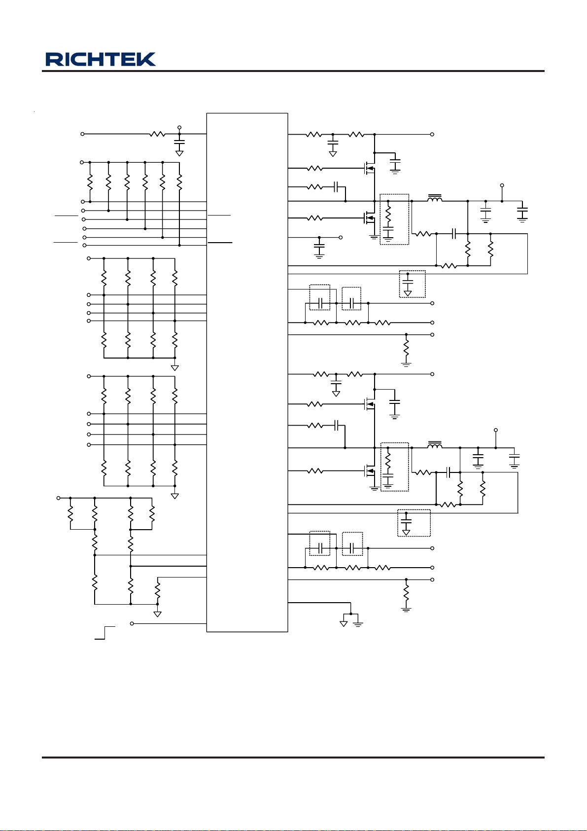
Function Block Diagram
VDIO
VCLK
ICCMAX
ICCMAXA
TMPMAX
ALERT
SETINIA
TSEN
SETINI
TSENA
EN
VR_READY
VCC
VRHOT
VRA_READY
RGNDA
FBA
COMPA
IBIAS
RGND
FB
COMP
ISEN1P
ISEN1N
From Control Logic
DAC
Soft-Start & Slew
Rate Control
From Control Logic
DAC
Soft-Start & Slew
Rate Control
SVID XCVR
V
REFA
+
-
V
REF
+
-
ERROR
AMP
ERROR
AMP
MUX
ADC
Offset
Cancellation
To Protection Logic
OCPOVP/UVP/NVP
Offset
Cancellation
UVLO
Control & Protection Logic
TON Time
PWM CMP
+
-
+
10
-
PWM CMP
+
-
To Protection Logic
+
10
-
OCP OVP/UVP/NVP
Generator
Driver Logic
Control
TON Time
Generator
Driver Logic
Control
GFXPS2
TONSETA
BOOTA
UGATEA
PHASEA
PVCC
LGATEA
ISENAP
ISENAN
OCSETA
TONSET
BOOT1
UGATE1
PHASE1
LGATE1
14
OCSET
DS8168B-00 November 2011www.richtek.com
Page 15

RT8168B
Absolute Maximum Ratings (Note 1)
z PVCC, VCC to GND ------------------------------------------------------------------------------------- −0.3V to 6.5V
z RGNDx to GND ------------------------------------------------------------------------------------------- −0.3V to 0.3V
z TONSETx to GND ---------------------------------------------------------------------------------------- −0.3V to 28V
z Others------------------------------------------------------------------------------------------------------- −0.3V to (V
z BOOTx to PHASEx-------------------------------------------------------------------------------------- −0.3V to 6.5V
z PHASEx to GND
DC------------------------------------------------------------------------------------------------------------ −3V to 28V
<20ns ------------------------------------------------------------------------------------------------------- −8V to 32V
z UGATEx to PHASEx
DC------------------------------------------------------------------------------------------------------------ −0.3V to (BOOTx − PHASEx)
<20ns ------------------------------------------------------------------------------------------------------- −5V to 7.5V
z LGA TEx to GND
DC------------------------------------------------------------------------------------------------------------ −0.3V to (PVCC + 0.3V)
<20ns ------------------------------------------------------------------------------------------------------- −2.5V to 7.5V
z Power Dissipation, P
D
@ T
= 25°C
A
WQFN−40L 5x5------------------------------------------------------------------------------------------- 2.778W
z Package Thermal Resistance (Note 2)
WQFN−40L 5x5, θJA------------------------------------------------------------------------------------- 36°C/W
WQFN−40L 5x5, θJC------------------------------------------------------------------------------------- 6°C/W
z Junction T emperature------------------------------------------------------------------------------------ 150°C
z Lead T e mperature (Soldering, 10 sec.)-------------------------------------------------------------- 26 0°C
z Storage T emperature Range --------------------------------------------------------------------------- −65°C to 150°C
z ESD Susceptibility (Note 3)
HBM (Human Body Mode) ----------------------------------------------------------------------------- 2kV
MM (Ma chine Mode)------------------------------------------------------------------------------------- 200V
+ 0.3V)
CC
Recommended Operating Conditions (Note 4)
z Supply Voltage, V
z Input V oltage, V
z Junction T emperature Range--------------------------------------------------------------------------- −40°C to 125°C
z Ambient T emperature Range--------------------------------------------------------------------------- −40°C to 85°C
------------------------------------------------------------------------------------- 4.5V to 5.5V
CC
----------------------------------------------------------------------------------------- 5V to 25V
IN
Electrical Characteristics
(V
= 5V, T
CC
Supply Input
Input Voltage Range
Supply Current
+ PVCC)
(V
CC
Supply Current
(TONSETx)
DS8168B-00 November 2011 www.richtek.com
= 25°C, unless otherwise specified)
A
Parameter Symbol Test Conditions Min Typ Max Unit
VCC/V
V
Battery Input Voltage 5 -- 25 V
IN
I
VCC
I
TONSETx
VEN = 1.05V, Not Switching 4.5 5 5.5 V
PVCC
+ I
VEN = 1.05V, Not Switching -- 12 20 mA
PVCC
V
=1 V, VIN = 12V, R
FB
= 100kΩ -- 110 -- μA
TON
To be continued
15
Page 16

RT8168B
Parameter Symbol Test Conditions Min Typ Max Unit
Shutdown Current
(P V CC + V
CC
)
Shutdown Current
(TONSETx)
I
VCC_SHDN
+ I
PVCC_SHDN
I
TONSETx_SHDN
= 0V -- -- 5 μA
V
EN
VEN = 0V -- -- 5 μA
TON Setting
TONS ETx Voltage V
TONSETx
On-Time tON I
TONSETx Input
Current Range
Mi n imum Off- T ime T
I
RTON
OFF_MIN
I
V
= 80μA, V
RTON
= 80μA, V
RTON
= 1.1V 25 -- 2 80 μA
FBx
-- 350 -- ns
GFX VR F o rce d DEM
GFXPS2x Enable
Threshold
GFXPS2x Disable
Threshold
V
GFXPS
V
GFXPS
4.3 -- -- V
-- -- 0.7 V
References and Syst em Output Vo ltage
DA C Accu rac y
(PS0/PS1)
SETINIx Voltage V
IBIAS Pin V olt age V
Dynamic VID Slew
Rate
V
FBx
SETINIx
IBIAS
SR
R
DVID
VID
OFS
VID
OFS
VID
OFS
VID
OFS
VID
OFS
V
INI_CORE
V
INI_CORE
V
INI_CORE
V
INI_CORE
Set VI D Slow 2.5 3.125 3.75
SetVID Fast 10 12.5 15
Setting = 1.000V~1.520V
SVID
Setting = 0V
SVID
Setting = 0.800V~1.000V
SVID
Setting = 0V
SVID
Setting = 0.500V~0.800V
SVID
Setting = 0V
SVID
Setting = 0.250V~0.500V
SVID
Setting = 0V
SVID
Setting = 1.100V
SVID
Setting = −0.640V~0.635V
SVID
= 0V, V
= 0.9V, V
= 1V, V
= 1.1V, V
= 53.6kΩ 2.09 2.14 2.19 V
IBIAS
= 1V 0.95 1. 075 1.2 0 V
FBx
= 1V 315 350 385 ns
FBx
−0.5 0 0.5 %VID
−5 0 5
−8 0 8
mV
−8 0 8
−10 0 10
INI_GFX
INI_GFX
= 0V 0 0.3125 0.5125
INI_GFX
= 0.9V 0.7375 0.9375 1. 1375
= 1V 1.3625 1.5625 1.7625
INI_GFX
= 1.1V 2.6125 -- 5
mV/μs
V
Error Amplifier
DC Gain ADC R
Gain-Bandwidth
Product
Sle w Rate SR
GBW C
COMP
= 47 k Ω (Note5) 70 80 -- dB
L
= 5pF (Note5) -- 10 -- MHz
LOAD
= 10pF (Gai n = −4,
C
LOAD
R
LOAD_COMP
0.5V to 3V)
Output Voltage
Range
MAX Source/Sink
Current
Impedance of FB x R
V
I
R
COMP
V
COMP
1 -- -- MΩ
FBx
= 47 k Ω 0.5 -- 3.6 V
L
= 2V -- 250 -- μA
COMP
16
= 47kΩ, V
COMPx
=
-- 5 -- V/μs
To be continued
DS8168B-00 November 2011www.richtek.com
Page 17

Current Sense Amplifier
RT8168B
Parameter Symbol Test Conditions Min Typ Max Unit
Input Offset V olt age V
Impedance of Neg. Input R
Impedance of Pos. Input R
Current Sense
Diffe re nti al Inpu t Ra nge
Current Sense DC Gain
(Loop)
V
Linear ity V
ISEN
Gate Driver
Upper Driver Source R
Upper Driver Sink R
Lower Driver Source R
L o wer Driv e r Si n k R
Internal Boot Charging
Switch On - R esista n c e
Zero Current Detection
Threshold
Protection
Under Volt age Lock- out
Threshold
Under Volt age Lock- out
Hysteresis
Over Voltage P rotection
Threshold
Under Volt age Pr ot ecti on
Threshold
Negative Vol tage
Pro te cti on Threshold
Curre nt Sense Ga in for
Over Current Protection
Logic Input s
OFS_CSA
ISENxN
ISENxP
V
CSDIx
V
A
I
ISEN_AC C
UGATEx_sr
UGATEx_sk
LGATEx_sr
LGATEx_sk
R
BOOTx
V
ZCD_TH
V
UVLO
ΔV
UVLO
V
OVP
V
UVP
V
NVP
A
OC
−1 -- 1 mV
1 -- -- MΩ
1 -- -- MΩ
= 1.1V,
V
FBx
V
CSDIx
FBx
V
DAC
V
BOOTx
V
BOOTx
V
UGATEx
= V
ISENxP
= 1.1V, −30mV < V
= 1.1V −30mV < V
− V
− V
= 0.1V -- 1 -- Ω
PHASEx
UGATEx
− V
= 5V
= 0.1V
PVCC = 5V, PVCC − V
V
= 0.1V -- 0.5 -- Ω
LGATEx
ISENxN
CSDIx
ISEN_IN
LGATEx
−50 -- 100 mV
< 50mV -- 10 -- V/V
< 50mV −1 -- 1 %
-- 1 -- Ω
= 0.1V -- 1 -- Ω
PVCC to BOOTx -- 30 -- Ω
V
ZCD_TH
= GN D − V
PHASEx
-- 10 -- mV
VCC Falling edge 4.04 4.24 -- V
-- 100 -- mV
V
Respect to VOUT_MAX
filte r time
= V
V
UVP
<1.52V, with 3μs filter time
= V
NVP
V
OCSET
V
ISENxP
ISENxN
ISENxN
= 2.4V
− V
ISENxN
− V
REFx
− GND −100 −50 -- mV
= 50mV
, with 1μs
SVID
, 0.8V < V
100 150 200 mV
REFx
−350 −300 −250 mV
-- 48 -- V/V
EN Input
Threshold
Voltage
Logic-High VIH With respe c t to 1V, 70% 0.7 -- --
Logic-Low V
With respe c t to 1V, 30% -- -- 0.3
IL
V
Leakage Current of EN −1 -- 1 μA
VCLK,VDIO Input
Threshold Vol tage
Leakage Current of
VC L K, VDI O
VIH With resp ect to In tel Sp ec. 0. 6 5 -- --
With resp ect to In tel Sp ec. -- -- 0.4 5
V
IL
I
LEAK_IN
−1 -- 1 μA
V
To be continued
DS8168B-00 November 2011 www.richtek.com
17
Page 18

RT8168B
ALERT
ALERT Low Voltage
VR Ready
VRx_READY Low Volta ge V
VRx_READY Delay t
Ther ma l T hro ttlin g
VRHOT Output V ol t age V
Hi gh Im peda nce Ou tp ut
V
ALERT
VRx_READY IVRx _REA D Y_ SINK
VRx_READY
VRHOT
I
ALE R T_ SINK
V
ISENxN
I
VRHOT_SINK
= V
= 4mA
BOOT
= 40mA
-- -- 0.4 V
= 4mA -- -- 0.4 V
to V
VRx_READY
high 70 100 160 μs
-- 0.4 -- V
Parameter Symbol Test Conditions Min Typ Max Unit
ALERT, VRx_REA DY,
VRHOT
Temp er ature Zon e
TSEN Threshold for
Tmp_Zone [7] transition
TSEN Threshold for
Tmp_Zone [6] transition
TSEN Threshold for
Tmp_Zone [5] transition
TSEN Threshold for
Tmp_Zone [4] transition
TSEN Threshold for
Tmp_Zone [3] transition
TSEN Threshold for
Tmp_Zone [2] transition
TSEN Threshold for
Tmp_Zone [1] transition
TSEN Threshold for
Tmp_Zone [0] transition
Update Period t
ADC
Latency t
I
LEAK_OUT
−1 -- 1 μA
100°C -- 1.8725 -- V
97°C -- 1.8175 -- V
V
TSENx
94°C -- 1.7625 -- V
91°C -- 1.7075 -- V
88°C -- 1.6525 -- V
85°C -- 1.5975 -- V
V
TSENx
82°C -- 1.5425 -- V
75°C -- 1.4875 -- V
-- 1600 -- μs
TSEN
-- -- 400 μs
LAT
C
ICCMAX1
V
ICCMAX
= 0.637V 29 32 35 decimal
Digital Code of ICCMAX
18
C
ICCMAX2
C
ICCMAX3
C
ICCMAXA1
C
ICCMAXA2
C
ICCMAXA3
C
TMPMAX1
C
TMPMAX2
C
TMPMAX3
V
ICCMAX
V
ICCMAX
V
ICCMAXA
V
ICCMAXA
V
ICCMAXA
V
TMPMAX
V
TMPMAX
V
TMPMAX
= 1.2642V 61 64 67 decimal
= 2.5186V 125 128 131 decimal
= 0.16 66V 5 8 11 decimal
= 0.3234V 13 16 19 decimal Digital Code of ICCMAXA
= 0.637V 29 32 35 decimal
= 1.6758V 82 85 88 decimal
= 1.9698V 97 100 103 decimal Dig ital Code of TMPMA X
= 2.4598V 122 125 128 decimal
DS8168B-00 November 2011www.richtek.com
Page 19

RT8168B
Note 1. Stresses listed as the above “Absolute Maximum Ratings” may cause permanent damage to the device. These are for
stress ratings. Functional operation of the device at these or any other conditions beyond those indicated in the
operational sections of the specifications is not implied. Exposure to absolute maximum rating conditions for extended
periods may remain possibility to affect device reliability.
Note 2. θ
Note 3. Devices are ESD sensitive. Handling precaution is recommended.
Note 4. The device is not guaranteed to function outside its operating conditions.
Note 5. Guaranteed by design.
is measured in the natural convection at TA = 25°C on a high effective thermal conductivity four-layer test board of
JA
JEDEC 51-7 thermal measurement standard. The measurement case position of θ
package.
is on the exposed pad of the
JC
DS8168B-00 November 2011 www.richtek.com
19
Page 20

RT8168B
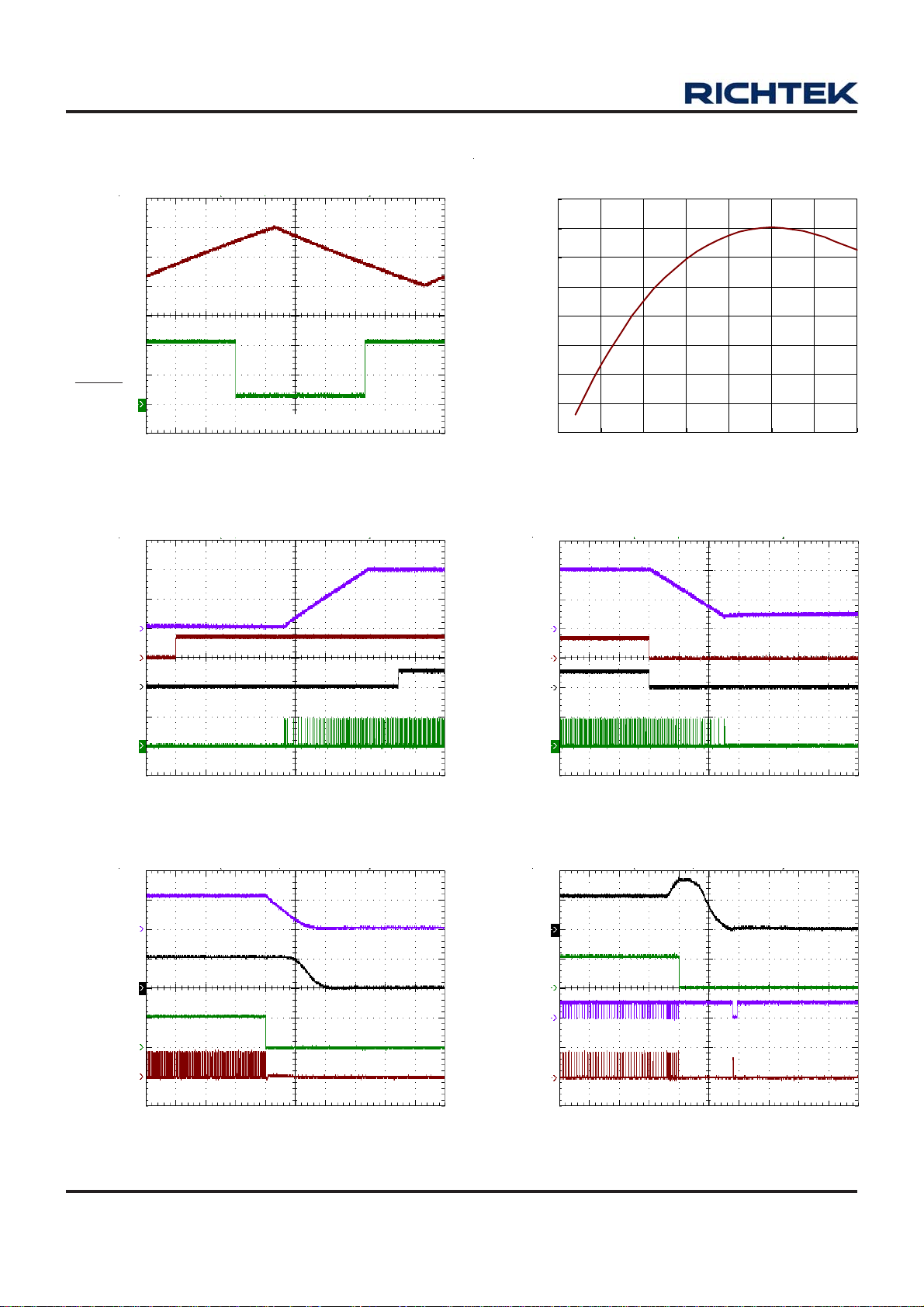
Typical Operating Characteristics
V
CORE
(500mV/Div)
EN
(2V/Div)
VR_READY
(2V/Div)
UGATE
(20V/Div)
V
CORE
(1V/Div)
CORE VR Power On from EN
Boot VID = 1V
Time (100μs/Div)
CORE VR OCP
V
CORE
(500mV/Div)
EN
(2V/Div)
VR_READY
(2V/Div)
UGATE
(20V/Div)
V
CORE
(1V/Div)
CORE VR Power Off from EN
Boot VID = 1V
Time (100μs/Div)
CORE VR OVP and NVP
I
LOAD
(10A/Div)
VR_READY
(1V/Div)
UGATE
(20V/Div)
V
CORE
(500mV/Div)
VCLK
(2V/Div)
VDIO
(2V/Div)
ALERT
(2V/Div)
VID = 1.1V
Time (100μs/Div)
CORE VR Dynamic VID Up
0.7V to 1.2V, Slew Rate = Slow, I
LOAD =
4A
LGATE
(10V/Div)
VR_READY
(1V/Div)
UGATE
(20V/Div)
V
CORE
(500mV/Div)
VCLK
(2V/Div)
VDIO
(2V/Div)
ALERT
(2V/Div)
VID = 1.1V
Time (40μs/Div)
CORE VR Dynamic VID Down
1.2V to 0.7V, Slew Rate = Slow, I
LOAD =
4A
20
Time (40μs/Div)
Time (40μs/Div)
DS8168B-00 November 2011www.richtek.com
Page 21

RT8168B
V
CORE
(500mV/Div)
VCLK
(2V/Div)
VDIO
(2V/Div)
ALERT
(2V/Div)
V
CORE
(20mV/Div)
CORE VR Dynamic VID Up
0.7V to 1.2V, Slew Rate = Fast, I
Time (10μs/Div)
CORE VR Load Transient
LOAD =
4A
V
CORE
(500mV/Div)
VCLK
(2V/Div)
VDIO
(2V/Div)
ALERT
(2V/Div)
V
CORE
(20mV/Div)
CORE VR Dynamic VID Down
1.2V to 0.7V, Slew Rate = Fast, I
Time (10μs/Div)
LOAD =
CORE VR Load Transient
4A
I
LOAD
(A/Div)
V
CORE
(20mV/Div)
VCLK
(1V/Div)
LGATE
(10V/Div)
UGATE
(20V/Div)
8
1
VID = 1.1V, I
1A to 8A, Slew Time = 150ns
LOAD =
Time (100μs/Div)
CORE VR Mode Transition
VID = 1.1V , PS0 to PS2, I
Time (100μs/Div)
LOAD =
0.2A
I
LOAD
(A/Div)
V
CORE
(20mV/Div)
VCLK
(1V/Div)
LGATE
(10V/Div)
UGATE
(20V/Div)
8
1
VID = 1.1V, I
8A to 1A, Slew Time = 150ns
LOAD =
Time (100μs/Div)
CORE VR Mode Transition
VID = 1.1V , PS2 to PS0, I
Time (100μs/Div)
LOAD =
0.2A
DS8168B-00 November 2011 www.richtek.com
21
Page 22
RT8168B
1.9
TSEN
(V/Div)
1.7
VRHOT
(500mV/Div)
V
GFX
(500mV/Div)
EN
(2V/Div)
VRA_READY
(2V/Div)
CORE VR Thermal Monitoring
TSEN Sweep from 1.7V to 1.9V
Time (10ms/Div)
GFX VR Power On from EN
1.006
1.004
1.002
1.000
(V)
0.998
REF
V
0.996
0.994
0.992
0.990
V
GFX
(500mV/Div)
EN
(2V/Div)
VRA_READY
(2V/Div)
CORE VR V
-50 -25 0 25 50 75 100 125
vs. Temperature
REF
Temperature (°C)
GFX VR Power Off from EN
UGATEA
(20V/Div)
V
GFX
(1V/Div)
I
LOAD
(5A/Div)
VRA_READY
(1V/Div)
UGATEA
(20V/Div)
Time (100μs/Div)
GFX VR OCP
Time (100μs/Div)
Boot VID = 1V
UGATEA
(20V/Div)
V
GFX
(1V/Div)
VRA_READY
(1V/Div)
LGATEA
(10V/Div)
UGATEA
(20V/Div)
Boot VID = 1V
Time (100μs/Div)
GFX VR OVP and NVP
VID = 1.1V
Time (40μs/Div)
22
DS8168B-00 November 2011www.richtek.com
Page 23

RT8168B
V
GFX
(500mV/Div)
VCLK
(2V/Div)
VDIO
(2V/Div)
ALERT
(2V/Div)
V
GFX
(500mV/Div)
GFX VR Dynamic VID
0.7V to 1.2V, Slew Rate = Slow, I
Time (40μs/Div)
GFX VR Dynamic VID
LOAD =
1.25A
V
GFX
(500mV/Div)
VCLK
(2V/Div)
VDIO
(2V/Div)
ALERT
(2V/Div)
V
GFX
(500mV/Div)
GFX VR Dynamic VID
1.2V to 0.7V, Slew Rate = Slow, I
Time (40μs/Div)
GFX VR Dynamic VID
LOAD =
1.25A
VCLK
(2V/Div)
VDIO
(2V/Div)
ALERT
(2V/Div)
V
GFX
(20mV/Div)
I
LOAD
(A/Div)
4
1
0.7V to 1.2V, Slew Rate = Fast, I
Time (10μs/Div)
GFX VR Load Transient
VID = 1.1V, I
1A to 4A, Slew Time = 150ns
LOAD =
LOAD =
1.25A
VCLK
(2V/Div)
VDIO
(2V/Div)
ALERT
(2V/Div)
V
GFX
(20mV/Div)
I
LOAD
(A/Div)
4
1
1.2V to 0.7V, Slew Rate = Fast, I
Time (10μs/Div)
GFX VR Load Transient
VID = 1.1V, I
4A to 1A, Slew Time = 150ns
LOAD =
LOAD =
1.25A
Time (100μs/Div)
Time (100μs/Div)
DS8168B-00 November 2011 www.richtek.com
23
Page 24

RT8168B
V
GFX
(20mV/Div)
VCLK
(1V/Div)
LGATEA
(10V/Div)
UGATEA
(20V/Div)
1.9
TSENA
(V/Div)
1.7
GFX VR Mode Transition
VID = 1.1V , PS0 to PS2, I
Time (100μs/Div)
LOAD =
GFX VR Thermal Monitoring
0.1A
V
GFX
(20mV/Div)
VCLK
(1V/Div)
LGATEA
(10V/Div)
UGATEA
(20V/Div)
1.006
1.004
1.002
1.000
0.998
(V)
0.996
REF
V
0.994
GFX VR Mode Transition
VID = 1.1V , PS2 to PS0, I
Time (100μs/Div)
GFX VR V
vs. Temperature
REF
LOAD =
0.1A
VRHOT
(500mV/Div)
TSENA Sweep from 1.7V to 1.9V
Time (10ms/Div)
0.992
0.990
0.988
-50-250 255075100125
Temperature (°C )
24
DS8168B-00 November 2011www.richtek.com
Page 25

Application Information
RT8168B
The RT8168B is a VR12/IMVP7 compliant, dual singlephase synchronous Buck PWM controller for the CPU
CORE VR a nd GFX VR. The gate drivers are embedded
to facilitate PCB design a nd reduce the total BOM cost. A
serial VID (SVID) interface is built-in in the RT8168B to
communicate with Intel VR12/IMVP7 complia nt CPU.
The RT8168B adopts G-NAVPTM (Green Native AVP),
which is Richtek's proprietary topology derived from finite
DC gain compensator, making it an easy setting PWM
controller to meet AVP requirements. The load line can
be ea sily progra mmed by setting the DC gain of the error
amplif ier. The RT8168B has fast transient response due
to the G-NAVPTM commanding variable switching
frequency .
G-NAVPTM topology also represents a high efficiency
system with green power concept. With G-NAVP
topology , the RT8168B becomes a green power controller
with high efficiency under heavy load, light load, a nd very
light load conditions. The RT8168B supports mode
transition function between CCM a nd DEM. These dif ferent
operating states allow the overall power system to have
low power loss. By utilizing the G-NAVPTM topology , the
operating frequency of RT8168B varies with output voltage,
load and VIN to further enhance the eff iciency even in CCM.
The built-in high accuracy DAC converts the SVID code
ranging from 0.25V to 1.52V with 5mV per step. The
differential remote output voltage sense a nd high accura cy
DAC allow the system to have high output voltage accura cy.
TM
The RT8168B supports VR12/IMVP7 compatible power
management states a nd VID on-the-fly function. The power
management states include DEM in PS2/PS3 and ForcedCCM in PS1/PS0. The VID on-the-fly function has three
different slew rates : Fa st, Slow and Decay . The RT8168B
integrates a high accuracy ADC for platform setting
functions, such as no-load offset and over current level.
The controller supports both DCR and sense-resistor
current sensing. The RT8168B provides VR ready output
signals of both CORE VR and GFX VR. It also features
complete fault protection functions including over voltage,
under voltage, negative voltage, over current and under
voltage lockout. The RT8168B is available in a WQFN48L 6x6 small foot print package.
Design Tool
T o help users reduce eff orts and errors caused by ma nual
calculations, a user-friendly design tool is now available
on request. This design tool calculates all necessary
design parameters by entering user's requirements.
Plea se conta ct Richtek's representatives for details.
Serial VID (SVID) Interface
SVID is a three-wire seri al synchronous interface defined
by Intel. The three wire bus includes VDIO, VCLK and
ALERT signals. The master (Intel's VR12/IMVP7 CPU)
initiates and termin ates SVID tra nsa ctions a nd drives the
V DIO, VCLK, and ALERT during a transa ction. The slave
(RT8168B) receives the SVID transactions and acts
accordingly.
DS8168B-00 November 2011 www.richtek.com
25
Page 26

RT8168B
Standard Serial VID Command
Code Commands
00h not supported N/A N/A N/A
01h SetVID_Fast VID code N/A
02h SetVID_Slow VID code N/A
03h SetVID_Decay VID code N/A
04h SetPS
05h SetRegADR
06h SetReg DAT
07h GetReg
08h
-
1Fh
not supported N/A N/A N/A
Master Payload
Contents
Byte indicating
po wer states
Pointer of registers
in data table
New data regis ter
content
Pointer of registers
in data table
Slave Pa yload
Contents
Set new tar get VID code, VR jumps t o new VID
target with controlled default “fast” slew rate
12.5mV /μs.
Set new tar get VID code, VR jumps t o new VID
target with controlled default “slow” slew rate
3.125mV/μs.
Set new tar get VID code, VR jumps t o new VID
target, but does not control the slew rate. The
output voltage decays at a rate proporti onal to
the load current
N/A Set power state
N/A Set the pointer of the data register
N/A Write t he cont ents t o the dat a register
Specified
Register
Contents
Slave returns the contents of the specified
register as the payload
Description
26
DS8168B-00 November 2011www.richtek.com
Page 27

RT8168B
Data and Configuration Register
Index Register Name Description Access Default
00h Vendor ID Vendor ID, default 1Eh. RO, Ve ndor 1 Eh
01h Product ID Product ID. RO, Ve ndor 65h
02h Product Revisi on Produ ct Rev ision. RO, Ve ndor 01h
05h Protocol ID SVID Protocol ID. RO, Vendor 01h
Bit mapped regis t er , iden ti fies th e SVID VR capabilities
06h VR_Capability
10h Status _1 Data registe r containing the st at us of V R. R-M, W-PWM 00h
11h Status-2 Data regi ste r con tai ni ng the st at us of tra nsmi ssi on. R-M, W-PWM 00h
12h
Temperature
Zone
15h Output_Current
1Ch St at us_2_l as t re ad The registe r contai ns a c opy of the st atus_2. R-M, W-P WM 00h
21h ICC_Max
22h Temp_Max
24h SR-Fast
and which of the optional telemetry register are
suppor ted.
Data registe r show i ng temper at ur e zone that have been
entered.
Data regi ste r show i ng direc t AD C con v er sion of aver aged
output current.
Data register containi ng the maximum ICC of platform
supports.
Binary form at in Amp, IE 64h = 100A.
Data re gister c ont ai ning the tempe ra tu re max the platform
supports.
Binary form at in °C , IE 64h = 100°C
Only for CORE VR
Data reg ister c ont ai ning the capability of fast slew rate th e
platform can sustains. Binary format in mV/μs, IE 0Ah =
10mV/μs.
RO, Ve ndor 81h
R-M, W-PWM 00h
R-M, W-PWM 00h
RO, Platform --
RO, Platform --
RO 0Ah
25h SR-Slow
30h VOUT_Max
Data register containing the capability of slow slew rate.
Binary format in mV/μs IE 02h = 2.5mV/μs.
The registe r i s programm ed by the master and sets the
maximum VID.
RO 02h
RW , Master B Fh
31h VID Se tting Da ta regis te r con taining currently pro gra mmed V ID . RW , Master 00h
32h Power State Register containing the current programmed power state. RW, Master 00h
33h Off set Se t offset in V ID step s. RW, Master 00h
34h Mult i VR Config
35h Pointer
Notes :
RO = Read Only
RW = Read/Write
R-M = Read by Master
W -PWM = Write by PWM only
Vendor = hard coded by VR vendor
Platform = programmed by platform
Master = programmed by the master
PWM = programmed by the VR control IC
Bit mapped dat a register which configures multiple V Rs
behav ior on the same bus.
Scratch pad register for tempor ary storage of the
SetRegADR pointer register.
RW, Master 00h
RW, Master 30h
DS8168B-00 November 2011 www.richtek.com
27
Page 28

RT8168B
Power Ready Detection and Power On Reset (POR)
During start-up, the RT8168B detects the voltage on the
voltage input pins : VCC and EN. When VCC > V
UVLO
the RT8168B will recognize the power state of system to
be ready (POR = high) and wait for enable command at
EN pin. After POR = high and EN > V
, the RT8168B
ENTH
will enter start-up sequence for both CORE VR a nd GFX
VR. If the voltage on any voltage pin drops below POR
threshold (POR = low), the RT8168B will enter power down
sequence and all the functions will be disa bled. SVID will
be invalid within 300μs after chip becomes enabled. All
the protection latches (OVP, OCP, UVP, OTP) will be
cleared only after POR = low. EN = low will not clear
these latches.
VCC
EN
V
V
U
V
E
N
+
L
O
-
+
-
T
H
POR
Chip EN
Figure 3. Power Ready Detection and Power On Reset
(POR)
Precise Reference Current Generation
The RT8168B includes extensive analog circuits inside
the controller. These analog circuits need very precise
reference voltage/current to drive these analog devices.
The RT8168B will auto-generate a 2.14V voltage source
at IBIAS pin, and a 53.6kΩ resistor is required to be
connected between IBIAS and analog ground. Through
this connection, the RT8168B generates a 40μA current
from IBIAS pin to analog ground a nd this 40μA current will
be mirrored inside the RT8168B for internal use. Other
types of connection or other values of resistance a pplied
at the IBIAS pin may cause failure of the RT8168B's analog
circuits. Thus a 53.6kΩ resistor is the only recommended
component to be connected to the IBIAS pin. The
resistance accuracy of this resistor is recommended to
be at least 1%.
Current
2.14V
-
Mirror
+
+
-
IBIAS
53.6k
Figure 4. IBIAS Setting
ICCMAX, ICCMAXA and TMPMAX
The RT8168B provides ICCMAX, ICCMAXA a nd TMPMAX
pins for platform users to set the maximum level of output
,
current or VR temperature: ICCMAX for CORE VR
maximum current, ICCMAXA for GFX VR maximum
current, and TMPMAX for CORE VR maximum
temperature.
To set ICCMAX, ICCMAXA and TMPMAX, platform
designers should use resistive voltage dividers on these
three pins. The current of the divider should be several
milli-Amps to avoid noise effect. The three items share
the same algorithms : the ADC divides 5V into 255 levels.
Therefore, LSB = 5/255 = 19.6mV , which mea ns 19.6mV
applied to ICCMAX pin equals to 1A setting. For exa mple,
if a platform designer wants to set TMPMAX to 120°C, the
voltage applied to TMPMAX should be 120 x 19.6mV =
2.352V. The ADC circuit inside these three pins will
decode the voltage a pplied and store the maximum current/
temperature setting into ICC_MAX and Temp_Max
registers. The ADC monitors a nd decodes the voltage at
these three pins only after EN = high. If EN = low, the
RT8168B will not take a ny action even when the V R output
current or temperature exceeds its maximum setting at
these ADC pins. The maximum level settings at these
ADC pins are different from over current protection or over
temperature protection. That mea ns, these maximum level
setting pins are only for platform users to define their
system operating conditions and these messages will only
be utilized by the CPU.
A/D
Converter
ICCMAX
ICCMAXA
TMPMAX
V
CC
Figure 5. ADC Pins Setting
V
INI_CORE
The initial start up voltage (V
and V
INI_GFX
Setting
INI_CORE
, V
INI_GFX
RT8168B can be set by platform users through SETINI
and SETINIA pins. V oltage divider circuit is recommended
to be applied to SETINI a nd SETINIA pins. The V
V
relate to SETINI/SETINIA pin voltage setting as
INI_GFX
shown in Figure 6. Recommended voltage setting at SETINI
and SETINIA pins are also shown in Figure 6.
) of the
INI_CORE
/
28
DS8168B-00 November 2011www.richtek.com
Page 29

RT8168B
V
(
C
C
5
V
)
V
N
I
V
V
V
N
I
V
V
=
1
.
1
I
_
C
O
I
_
I
G
N
_
I
C
N
I
V
I
N
I
_
O
I
C
I
_
I
G
N
_
I
C
N
I
V
I
N
I
V
E
R
1
=
.
1
V
F
X
2
1
/
V
C
C
=
1
V
O
E
R
=
1
V
_
G
F
X
4
1
/
V
C
=
0
.
9
V
R
E
=
0
.
9
V
F
X
0
=
V
O
E
R
0
=
V
_
G
F
X
C
8
1
/
V
C
C
D
G
N
Figure 6. SETINI and SETINIA Pin Voltage Setting
Start Up Sequence
The RT8168B utilizes internal soft-start sequence which
strictly follows Intel VR12/IMVP7 start up sequence
specifications. After POR = high a nd EN = high, a 300μs
delay is needed for the controller to determine whether all
the power inputs are ready for entering start up sequence.
If pin voltage of SETINI/SETINIA is zero, the output voltage
of CORE/GFX VR is programmed to stay at 0V. If pin
voltage of SETINI/SETINIA is not zero, VR output voltage
will ramp up to initi al boot voltage (V
INI_CORE
, V
INI_GFX
) after
both POR = high and EN = high. After the output voltage
of CORE/GFX VR rea ches target initial boot voltage, the
controller will keep the output voltage at the initial boot
voltage and wait for the next SVID commands. After the
RT8168B receives valid VID code (typically SetVID_Slow
command), the output voltage will ramp up/down to the
target voltage with specified slew rate. After the output
voltage reaches the target voltage, the RT8168B will send
out VR_READY signal to indicate the power state of the
RT8168B is ready. The VR_READY circuit is an opendrain structure so a pull-up resistor is recommended for
connecting to a voltage source.
V
INI_CORE
V
INI_GFX
1.1V
0.9V
1V
0V
Recommended
SETINI/SETINIA Pin Voltage
5
x VCC≒3.125V or VCC
8
3
x VCC≒1.875V
8
3
x VCC≒0.9375V
16
1
x VCC≒0.3125V or GND
16
Power Down Sequence
Similar to the start up sequence, the RT8168B also utilizes
a soft shutdown mechanism during turn-off. After POR =
low, the internal reference voltage (positive terminal of
compensation EA) starts ra mping down with 3.125mV/μs
slew rate, and output voltage will follow the reference
voltage to 0V . After output voltage drops below 0.2V, the
RT8168B shuts down and all functions are disa bled. The
VR_READY will be pulled down immediately after POR =
low.
DS8168B-00 November 2011 www.richtek.com
29
Page 30

RT8168B
VCC
POR
EN Chip
(Internal Signal)
EN
SVID
V
CORE
CORE VR
Operation Mode
V
GFX
GFX VR
Operation Mode
VR_READY
VRA_READY
VCC
XX
300µs
Off
Off
CCM CCM
CCM
100µs
Figure 7 (a). Power sequence for RT8168B (V
POR
Valid xx
0.2V
SVID defined
SVID defined
100µs
INI_CORE
= V
CCM
INI_GFX
= 0V)
Off
0.2V
Off
EN
EN Chip
(Internal Signal)
SVID
V
CORE
CORE VR
Operation Mode
VR_READY
V
GFX
GFX VR
Operation Mode
VRA_READY
300µs
XX
250µs
50µs
V
INI_CORE
CCM CCMOff
100µs
V
INI_GFX
CCMOff
100µs
Valid
SVID define d
SVID define d
Figure 7 (b). Power sequence for RT8168B (V
INI_CORE
CCM
0, V
≠ ≠
INI_GFX
xx
0.2V
Off
0.2V
Off
0V)
30
DS8168B-00 November 2011www.richtek.com
Page 31

RT8168B
Disable GFX VR : Before EN = High
GFX VR enable or disable is determined by the internal
circuitry that monitors the ISENAN voltage during start
up. Before EN = high, GFX V R detects whether the voltage
of ISENAN is higher than “VCC − 1V” to disable GFX
VR. The unused driver pins ca n be connected to GND or
left floating.
GFX VR Forced-DEM Function Enable : After
VRA_Ready = High
The GFX VR's forced-DEM function can be enabled or
disabled with GFXPS2 pin. The RT8168B detects the
voltage of GFXPS2 f or forced-DEM function. If the voltage
at GFXPS2 pin is higher tha n 4.3V , the GFX V R operates
in forced-DEM. If this voltage is lower than 0.7V, the GFX
VR follows SVID power state comma nd.
Loop Control
Both CORE and GFX VR adopt Richtek's proprietary GNAVPTM topology . G-NA VPTM is based on the f inite-gain
valley current mode with CCRCOT (Constant Current
Ripple Constant On Time) topology. The output voltage,
V
CORE
or V
, will decrease with increasing output load
GFX
current. The control loop consists of PWM modulator with
power stage, current sense amplifier and error amplifier
a s shown in Figure 8.
V
IN
V
OUT
(V
CORE/VGFX
C
X
CORE/GFX VR
V
CC_SENSE
GFX/CORE VR
CCRCOT
PWM Generator
CMP
+
-
V
CSx
EA
+
Driver
Logic
Control
+
Ai
-
VREFx
-
+
UGATEx
PHASEx
LGATEx
ISENxP
ISENxN
COMPx
FBx
RGNDx
High Side
MOSFET
Low Side
MOSFET
C
Byp
C2 C1
R2
CORE/GFX VR
V
SS_SENSE
R1
L
R
X
Figure 8. Simplified Schematic for Droop a nd Remote
Sense in CCM
Similar to the valley current mode control with finite
compensator gain, the high side MOSFET on-time is
determined by the CCRCOT PWM generator. When load
current increas es, VCS increa ses, the steady state COMP
voltage also increases which makes the output voltage
decrea se, thus achieving AVP .
Droop Setting (with Temperature Compensation)
It's very easy to achieve the Active Voltage Positioning
(AVP) by properly setting the error amplifier gain due to
the native droop characteristics. The target is to have
V
= V
OUT
Then solving the switching condition V
REFx
− I
LOAD
x R
(1)
DROOP
COMPx
= V
CSx
in
Figure 8 yields the desired error amplif ier gain a s
==
A
V
R2
R1 R
I SENSE
DROOP
(2)
×
AR
where AI is the internal current sense amplifier gain and
R
is the current sense resistance. If no external sens e
SENSE
resistor is present, the DCR of the inductor will act as
R
SENSE
. R
is the resistive slope value of the converter
DROOP
output and is the desired static output impedance.
V
OUT
)
0
Figure 9. Error Amplifier Gain (AV) Influence on V
R
C
C
A
> A
V2
Load Current
Accuracy
V1
A
V2
A
V1
OUT
Since the DCR of inductor is temperature dependent, it
affects the output accura cy in high temperature conditions.
Temperature compensation is recommended for the
lossless inductor DCR current sense method. Figure 10
shows a simple but effective way of compensating the
temperature variations of the sense resistor using a n N TC
thermistor placed in the feedba ck path.
C2 C1
EA
FBx
R2
V
SS_SENSE
COMPx
-
+
-
+
RGNDx
VREFx
R1b
R1a
NTC
V
CC_SENSE
Figure 10. Loop Setting with T emperature Compensation
DS8168B-00 November 2011 www.richtek.com
31
Page 32

RT8168B
)()
}
Usually, R1a is set to equal R
(25°C), while R1b is
NTC
selected to linearize the NTC's temperature chara cteristic.
For a given NTC, the design would be to obtain R1b a nd
R2 and then C1 a nd C2. According to (2), to compensate
the temperature variations of the sense resistor , the error
amplifier gain (AV) should have the same temperature
coefficient with R
AR
V, HOT SENSE, HOT
AR
V, COLD SENSE, COLD
=
SENSE
. Hence
(3)
From (2), we can have Av at a ny temperature (T) a s
A
=
V, T
R1 a / /R R1b
R2
NTC, T
+
(4)
The standard formula f or the resistance of NTC thermistor
as a function of te mperature is given by :
⎡⎤
11
β−
(
{
⎢⎥
T+273 298
RR e
where R
=
NTC, T NTC, 25
is the thermistor's nominal resistance at
NTC, 25
⎣⎦
(5)
room temperature, β (beta) is the thermistor's material
constant in Kelvins, and T is the thermistor's actual
temperature in Celsius.
The DCR value at different te mperatures can be calculated
using the equation below :
DCRT = DCR25 x [1+0.00393 x (T-25)] (6)
Loop Compensation
Optimized compensation of the CORE VR allows for best
possible load step response of the regulator's output. A
type-I compensator with one pole and one zero is adequate
for a proper compensation. Figure 10 shows the
compensation circuit. It wa s previously mentioned that to
determine the resistive feedback components of error
amplifier gain, C1 and C2 must be calculated for the
compensation. The target is to a chieve constant resistive
output impedance over the widest possible frequency
range.
The pole frequency of the compensator must be set to
compensate the output ca p acitor ESR zero :
f
=
P
1
2CR
×π× ×
C
where C is the cap acita nce of the output capa citor and R
(9)
C
is the ESR of the output cap acitor. C2 ca n be calculated
as follows :
CR
×
C2
=
C
R2
(10)
The zero of compensator has to be placed at half of the
switching frequency to filter the switching-related noise.
Such that,
C1
=
R1 b R1a// R f
+×π×
()
1
NTC, 25 C SW
°
(11)
where 0.00393 is the temperature coefficient of copper.
For a given NTC thermistor , solving (4) at room temperature
(25°C) yields
R2 = A
where A
x (R1b + R1a // R
V, 25
is the error amplif ier gain at room temperature
V, 25°C
) (7)
NTC, 25
obtained from (2). R1b can be obtained by substituting
(7) to (3),
R1 b
=
R
SENSE, HOT
R
SENSE, COLD
32
(R1a//R ) (R1a//R )
×−
NTC, HOT NT C, COLD
R
⎛⎞
SENSE, HOT
1
−
⎜⎟
R
SENSE, COLD
⎝⎠
(8)
TON Setting
High frequency operation optimizes the application by
trading off efficiency due to higher switching losses with
smaller component size. This may be acceptable in ultraportable devices where the load currents are lower and
the controller is powered from a lower voltage supply . Low
frequency operation offers the best overall efficiency at
the expense of component size and board spa ce. Figure
11 shows the on-time setting circuit. Connect a resistor
(R
TONSETx
) between VIN and T ONSETx to set the on-time
of UGA TEx :
t (V 1.2V)
ONx REFx
where t
<=
is the UGA TEx turn on period, VIN is the input
ONx
28 10 R
voltage of converter, and V
VV
IN REFx
REFx
TONSETx
(12)
−
is the internal reference
-12
××
voltage.
DS8168B-00 November 2011www.richtek.com
Page 33

RT8168B
When V
is larger than 1.2V, the equivalent switching
REFx
frequency may be over the maximum design range, ma king
it unaccepta ble. Therefore, the VR i mplements a pseudoconstant-frequency technology to avoid this disadva ntage
of CCRCOT topology. When V
is larger than 1.2V,
REFx
the on-time equation will be modified to :
t (V 1.2V)
ONx REFx
≥
-12
×× ×
23.33 10 R V
=
TONSETx REFx
−
VV
IN REFx
(13)
On-time tran slates roughly to switching frequencies. The
on-times guara nteed in the Electrical Characteristics are
influenced by switching delays in external high side
MOSFET . Also, the dead-time effect increa ses the effective
on-time, reducing the switching frequency . It occurs only
in CCM during dynamic output voltage transitions when
the inductor current reverses at light or negative load
currents. With reversed inductor current, PHASEx goes
high earlier than normal, extending the on-time by a period
equal to the high side MOSFET rising dead time.
For better efficiency of the given load ra nge, the maximum
switching frequency is suggested to be :
f(kHz)
S(MAX)
VI R DCRR
REFx(MAX) LOAD(MAX) ON_LS FET DROOP
VI R R
IN(MAX) LOAD(MAX) ON_LS FET ON_HS FET
=×
tt
+× +−
+× −
1
−
ON HS Delay
−
⎡⎤
⎣⎦
⎡⎤
⎣⎦
−
−−
(14)
where f
is the turn on delay of high side MOSFET , V
Delay
is the maximum switching frequency, t
S(MAX)
HS-
REFx(MAX)
is the maximum application DAC voltage of application,
V
IN(MAX)
I
LOAD(MAX)
is the low side MOSFET R
side MOSFET R
R
DROOP
is the maximum application input voltage,
is the maximum load of a pplication, R
, R
DS(ON)
, DCRL is the inductor DCR, and
DS(ON)
ON_HS-FET
ON_LS-FET
is the high
is the load line setting.
Differential Remote Sense Setting
The CORE/GFX VR includes differential, remote-sense
inputs to eliminate the effects of voltage drops along the
PC board traces, CPU internal power routes and socket
contacts. The CPU contains on-die sense pins CORE/
GFX V
GFX V
CC_SENSE
SS_SENSE
and V
SS_SENSE
. Connect RGNDx to CORE/
. Connect FBx to CORE/GFX V
CC_SENSE
with a resistor to build the negative input path of the error
a mplifier. The precision voltage reference V
is referred
REFx
to RGND f or a ccurate remote sensing.
Current Sense Setting
The current sense topology of the CORE/GFX VR is
continuous inductor current sensing. Therefore, the
controller can be less noise sensitive. Low of fset amplif iers
are used for loop control and over current detection. The
internal current sense a mplifier gain (AI) is fixed to be 10.
The ISENxP and ISENxN denote the positive and negative
input of the current sense a mplifier .
Users can either use a current sense resistor or the
inductor's DCR f or current sensing. Using inductor's DCR
allows higher efficiency a s shown in Figure 12. To let
L
DCR
RC
=×
X
X
(15)
then the transient performance will be optimum. For
example, choose L = 0.36μH with 1mΩ DCR and
C
= 100nF, to yields for R
X
0.36 H
V
Ω×
CSx
μ
PHASEx
+
A
I
-
R3.6k
==Ω
X
1m 10 0nF
ISENxP
ISENxN
:
X
(16)
V
OUT
(V
CORE/VGFX
L
DCR
C
R
X
X
)
C
Byp
Figure 12. Lossless Inductor Sensing
GFX/CORE
VR CCRCOT
PWM
Generator
On-Time
TONSETx
VREFx
R
TONSETx
C1
R1
V
IN
Figure 1 1. On-Ti me Setting with RC Filter
DS8168B-00 November 2011 www.richtek.com
33
Page 34

RT8168B
Considering the inductance tolera nce, the resistor RX has
to be tuned on board by examining the tra nsient voltage.
If the output voltage transient has an initial di p below the
minimum load line requirement with a slow recovery, R
is too small. Vice versa, if the resista nce is too large the
output voltage transient will only have a small initial dip
and the recovery will be too fast, causing a ring-back.
Using current-sense resistor in series with the inductor
can have better a ccuracy , but the ef ficiency is a trade-off.
Considering the equivalent inductance (L
sense resistor, a RC f ilter is recommended. The RC filter
calculation method is similar to the above-mentioned
inductor DCR sensing method.
Operation Mode Transition
The RT8168B supports operation mode transition function
in CORE/GFX VR for the SetPS comma nd of Intel's VR12/
IMVP7 CPU. The default operation mode of the RT8168B's
CORE/GFX VR is PS0, which is CCM operation. The other
operation mode is PS2 (DEM operation).
) of the current
ESL
V
CC
R
X
TSENx
R
1
NTC
R
2
R
3
Figure 13. Thermal Monitoring Circuit
T o meet Intel's V R12/IMVP7 specification, platform users
have to set the TSEN voltage to meet the temperature
variation of VR from 75% to 100% VR max temperature.
For example, if the VR max temperature is 100°C, platform
users have to set the TSEN voltage to be 1.4875V when
VR temperature reaches 75°C and 1.8725V when VR
temperature reaches 100°C. Detailed voltage setting
versus temperature variation is shown in Table 2.
Thermometer code is implemented in the Temperature
Zone register.
After receiving SetPS command, the CORE/GFX V R will
immediately change to the new operation state. When
VR receives SetPS command of PS2 operation mode,
the VR operates as a DEM controller.
If VR receives dyna mic VID change command (SetVID),
VR will automatically enter PS0 operation mode. After
output voltage reaches target voltage, V R will stay at PS0
state and ignore former SetPS command. Only by
re-sending SetPS command after SetVID command will
VR be forced into PS2 operation state again.
Thermal Monitoring and Temperature Reporting
CORE/GFX VR provides thermal monitoring function via
sensing TSEN pin voltage. Through the voltage divider
resistors R1, R2, R3 and R
, the voltage of TSEN will
NTC
be proportional to VR temperature. When VR temperature
rises, the TSENx voltage also rises. The ADC circuit of
VR monitors the voltage variation at TSENx pin from 1.47V
to 1.89V with 55mV resolution, and this voltage is decoded
into digital format and stored into the Temperature Zone
register.
Table 2. Temperature Zone Register
Com parator Trip Poin t s
VRHOT
SVID
Thermal
Alert
Temperatures Scal ed to maximum =
100%
Voltage Represents A ssert bit
Minimu m L evel
b7 b6 b5 b4 b3 b2 b1 b0
100% 97% 94% 91% 88% 85% 82% 75%
1.855V 1.8V
TSE N Pin V o lt age
1.855 ≤ V
1.800 ≤ V
1.745 ≤ V
1.690 ≤ V
1.635 ≤ V
1.580 ≤ V
1.525 ≤ V
1.470 ≤ V
V
TSEN
TSEN
≤ 1.835 0 1 1 1_111 1
TSEN
≤ 1.780 0011_11 11
TSEN
≤ 1.725 0001_1 111
TSEN
≤ 1.670 0000_1 111
TSEN
≤ 1.615 0000_0111
TSEN
≤ 1.560 0000_001 1
TSEN
≤ 1.505 0000_000 1
TSEN
< 1.470 0000_0000
1.745V 1.69V 1.635V 1.58V 1.52
Temperature_Zone
Register Content
1111_1111
5V
1.47
V
34
DS8168B-00 November 2011www.richtek.com
Page 35

The RT8168B supports two temperature reporting,
VRHOT(hardware reporting) and ALERT(software
reporting), to fulfill VR12/IMVP7 specification. VRHOT is
an open-drain structure which sends out a ctive-low VRHOT
signals. When TSEN voltage rises above 1.855V (100%
of VR temperature), the VRHOT signal will be set to low .
When TSEN voltage drops below 1.8V (97% of VR
temperature), the VRHOT signal will be reset to high. When
TSEN voltage rises above 1.8V (97% of VR temperature),
The RT8168B will update the bit1 data from 0 to 1 in the
Status_1 register and a ssert ALER T . When TSEN voltage
drops below 1.745V (94% of VR temperature), VR will
update the bit1 data from 1 to 0 in the Status_1 register
and a ssert ALER T .
The temperature reporting function for the GFX VR can be
disabled by pulling TSENA pin to VCC in case the
temperature reporting function for the GFX VR is not used
or the GFX VR is disabled. When the GFX VR's
temperature reporting function is disabled, the RT8168B
will reject the SVID command of getting the
Temperature_Zone register content of the GFX VR.
However, note that the temperature reporting function f or
the CORE VR is always a ctive. CORE VR's temperature
reporting function can not be disabled by pulling TSEN
pin to VCC.
RT8168B
V
CC
R
OC1
OCSETx
R
OC2
Figure 14. OCP Setting without Temperature
Compensation
The current limit is triggered when inductor current
exceeds the current limit threshold I
V
. The driver will be forced to turn off UGATE until
OCSET
the over current condition is cleared. If the over current
condition remains valid for 15 PWM cycles, VR will trigger
OCP latch. Latched OCP forces both UGA TE a nd LGA TE
to go low. When OCP is triggered in one of VRs, the
other VR will enter into soft shutdown sequence. The OCP
latch mechanism will be masked when VRx_READY =
low, which mea ns that only the current li mit will be a ctive
when V
is ramping up to initi al voltage (or V
OUT
If inductor DCR is used a s the current sense component,
then temperature compensation is recommended for
protection under all conditions. Figure 15 shows a typical
OCP setting with temperature compensation.
V
CC
, defined by
LIMIT
REFx
).
Over Current Protection
The CORE/GFX VR compares a programmable current
limit set point to the voltage from the current sense a mplifier
output for Over Current Protection (OCP). The voltage
applied to OCSETx pin def ines the desired peak current
limit threshold I
V
OCSET
= 48 x I
LIMIT
LIMIT
:
x R
SENSE
(17)
Connect a resistive voltage divider from VCC to GND, with
the joint of the resistive divider connected to OCSET pin
a s shown in Figure 14. For a given R
V
⎛⎞
RR 1
=× −
OC1 OC 2
CC
⎜⎟
V
OCSET
⎝⎠
OC2
, then
(18)
R
OC1a
OCSETx
R
R
NTC
OC1b
OC2
Figure 15. OCP Setting with Temperature Compensation
Usually , R
nominal resistance at room temperature. Ideally, V
is selected to be equal to the thermistor's
OC1a
OCSET
is assumed to have the same temperature coefficient as
R
(Inductor DCR) :
SENSE
VR
OCSET, HOT SENSE, HOT
VR
OCSET, COLD SENSE, COLD
=
(19)
DS8168B-00 November 2011 www.richtek.com
35
Page 36

RT8168B
According to the basic circuit calculation, V
OCSET
can be
obtained at any temperature :
R
VV
OCSET, T CC
=×
R//R R R
OC1a NTC, T OC1b OC2
OC2
++
(20)
Re-write (19) from (20), to get V
R//R R R R
OC1a NTC, COLD OC1b OC2 SENSE, HOT
R//R R R R
OC1a NTC, HOT OC1b OC2 SENSE, COLD
++
++
at room temperature
OCSET
=
(21)
V
OCSET, 25
V
CC
Solving (21) and (22) yields R
R
OC2
α× − + −α ×
R
OC1b
(1)R2 R R
α− × +α× −
=
R
×
R//R R R
OC1a NTC, 25 OC1b OC2
OC2
++
and R
OC1b
(22)
OC2
=
RR (1)R
EQU, HOT EQU, COLD EQU, 25
V
CC
V
OCSET, 25
(1 )
×−α
(23)
=
EQU, HOT EQU, COLD
(1 )
−α
(24)
where
α=
R
SENSE, HOT
R DCR [1 0.00393 (T 25)]
SENSE, COLD 25 COLD
DCR [1 0.00393 (T 25)]
=
×+ × −
25 HOT
×+ × −
(25)
R
EQU, T
= R
OC1a
// R
(26)
NTC, T
Over Voltage Protection (OVP)
The over voltage protection circuit of CORE/GFX VR
monitors the output voltage via the ISENxN pin. The
supported maximum operating VID of VR (V
in the V out_Max register. Once V
ISENxN
exceeds “V
(MAX)
) is stored
(MAX)
+ 200mV”, OVP is triggered and latched. VR will try to
turn on low side MOSFETs and turn off high side
MOSFETs to protect CPU. When OVP is triggered by
the one of the VRs, the other VR will enter soft shutdown
sequence. A 10μs delay is used in OVP detection circuit
to prevent false trigger.
Negative Voltage Protection (NVP)
During OVP latch state, both CORE/GFX VRs also monitor
ISENxN pin for negative voltage protection. Since the OVP
latch will continuously turn on low side MOSFET of VR,
VR may suffer negative output voltage. Therefore, when
the voltage of ISENxN drops below −0.05V after triggering
OVP, VR will turn off low side MOSFETs while high side
MOSFET s remain off. The N VP function will be a ctive only
after OVP is triggered.
Under Voltage Protection (UVP)
Both CORE/GFX VR implement U nder V oltage Protection
(UVP). If ISENxN is less tha n V
by 300mV + V
REFx
OFFSET
VR will trigger UVP latch. The UVP latch will turn off both
high side and low side MOSFET s. When UVP is triggered
by one of the VRs, the other VR will enter into soft
shutdown sequence. The UVP mechanism is masked
when VRx_READY = low.
Under Voltage Lock Out (UVLO)
During normal operation, if the voltage at the VCC pin
drops below UVLO falling edge threshold, both VR will
trigger UVLO. The UVLO protection forces all high side
MOSFETs and low side MOSFETs off to turn off.
Inductor Selection
The switching frequency and ripple current determine the
inductor value as f ollows :
VV
−
Lt
MIN ON
IN OUT
=×
I
Ripple(MAX)
(27)
where tON is the UGA TE turn on period.
Higher inductance induces less ripple current a nd hence
higher efficiency . However, the tra deoff is a slower transient
response of the power stage to load tra nsients. This might
increase the need f or more output ca pacitors, thus driving
up the cost. Find a low-loss inductor having the lowest
possible DC resista nce that fits in the allotted dimensions.
The core must be large enough not to be saturated at the
peak inductor current.
,
36
DS8168B-00 November 2011www.richtek.com
Page 37

RT8168B
Output Capacitor Selection
Output capacitors are used to obtain high bandwidth for
the output voltage beyond the bandwidth of the converter
itself. Usually, the CPU manufacturer recommends a
capacitor configuration. Two different kinds of output
capacitors can be found, bulk capacitors closely located
to the inductors and ceramic output capacitors in close
proximity to the load. Latter ones are for mid-frequency
decoupling with very small ESR and ESL values while the
bulk ca pacitors have to provide enough stored energy to
overcome the low-frequency bandwidth ga p between the
regulator and the CPU.
Layout Consideration
Careful PC board layout is critical to achieving low
switching losses and clean, stable operation. The
switching power stage requires particular attention. If
possible, mount all of the power components on the top
side of the board with their ground terminals flushed
against one another . Follow these guidelines for optimum
PC board layout :
` The capa citor connected to the ISEN1N/ISENAN f or noise
decoupling is optional and it should also be pla ced close
to the ISEN1N/ISENAN pin.
` The NTC thermistor should be pla ced physically close
to the inductor for better DCR thermal compensation.
` Keep the high current paths short, especially at the
ground terminals.
` Keep the power traces a nd load connections short. This
is essential for high efficiency.
` When trade-offs in trace lengths must be made, it's
preferable to allow the inductor charging path to be made
longer than the discharging path.
` Place the current sense component close to the
controller. ISENxP a nd ISENxN connections for current
limit and voltage positioning must be made using Kelvin
sense connections to guarantee the current sense
accura cy . The PCB tra ce from the sense nodes should
be parallel to the controller.
` Route high-speed switching nodes away from sensitive
analog areas (COMPx, FBx, ISENxP, ISENxN, etc...)
` Special attention should be paid in placing the DCR
current sensing components. The DCR current sensing
capacitor and resistors must be placed close to the
controller.
DS8168B-00 November 2011 www.richtek.com
37
Page 38

RT8168B
Outline Dimension
D
E
e
A
A3
A1
D2
SEE DETAIL A
1
b
L
E2
1
2
1
2
DETAIL A
Pin #1 ID a nd T ie Bar Mark Option s
Note : The configuration of the Pin #1 identifier is optional,
but must be located within the zone indicated.
Dimensions In Millim eters Dime nsions In Inches
Symbol
Min Max Min Max
A 0.700 0.800 0.028 0.031
A1 0.000 0.050 0.000 0.002
A3 0.175 0.250 0.007 0.010
b 0.150 0.250 0.006 0.010
D 4.950 5.050 0.195 0.199
D2 3.250 3.500 0.128 0.138
E 4.950 5.050 0.195 0.199
E2 3.250 3.500 0.128 0.138
e 0.400 0.016
L 0.350 0.450
Richtek Technology Corporation
Headquarter
5F, No. 20, Taiyuen Street, Chupei City
Hsinchu, Taiwan, R.O.C.
Tel: (8863)5526789 Fax: (8863)5526611
0.014 0.018
W-Type 40L QFN 5x5 Package
Richtek Technology Corporation
Taipei Office (Marketing)
5F, No. 95, Minchiuan Road, Hsintien City
Taipei County, Taiwan, R.O.C.
Tel: (8862)86672399 Fax: (8862)86672377
Email: marketing@richtek.com
Information that is provided by Richtek Technology Corporation is believed to be accurate and reliable. Richtek reserves the right to make any change in circuit
design, specification or other related things if necessary without notice at any time. No third party intellectual property infringement of the applications should be
guaranteed by users when integrating Richtek products into any application. No legal responsibility for any said applications is assumed by Richtek.
DS8168B-00 November 2011www.richtek.com
38
Page 39

 Loading...