

Page 1
®
3A, 1MHz, Synchronous Step-Down Converter
RT8061A
General Description
The RT8061A is a high efficiency synchronous, step-down
DC/DC converter. Its input voltage ra nge from 2.7V to 5.5V
that provides an adjustable regulated output voltage from
0.6V to V
while delivering up to 3A of output current.
IN
The internal synchronous low on resistance power
switches increase efficiency and eliminate the need for
an external Schottky diode. The switching frequency is
fixed internally at 1MHz. The 100% duty cycle provides
low dropout operation, hence extending battery life in
portable systems. Current mode operation with internal
compensation allows the transient response to be
optimized over a wide range of loa ds and output ca pacitors.
The RT8061A is operated in PWM/PSM mode to a chieve
high efficiency for a wide load range. The RT8061A is
available in a W DFN-10L 3x3 pack age.
Ordering Information
RT8061A
Package Type
QW : WDFN-10L 3x3 (W-Type)
Lead Plating System
Z : ECO (Ecological Element with
Halogen Free and Pb free)
Note :
Richtek products are :
` RoHS compliant and compatible with the current require-
ments of IPC/JEDEC J-STD-020.
` Suitable for use in SnPb or Pb-free soldering processes.
Features
zz
High Efficiency : Up to 95%
z
zz
zz
z Low R
zz
Internal Switches : 69m
DS(ON)
ΩΩ
Ω/49m
ΩΩ
= 5V
zz
z Fixed Frequency : 1MHz
zz
zz
z No Schottky Diode Required
zz
zz
z 0.6V Reference Allows Low Output Voltage
zz
zz
z PWM/PSM Mode Operation
zz
zz
z Low Dropout Operation : 100% Duty Cycle
zz
zz
z OCP, UVP, OVP, OTP
zz
z RoHS Compliant and Halogen Free
Applications
z Portable Instruments
z Battery-Powered Equipment
z Notebook Computers
z Distributed Power Systems
z IP Phones
z Digital Camera s
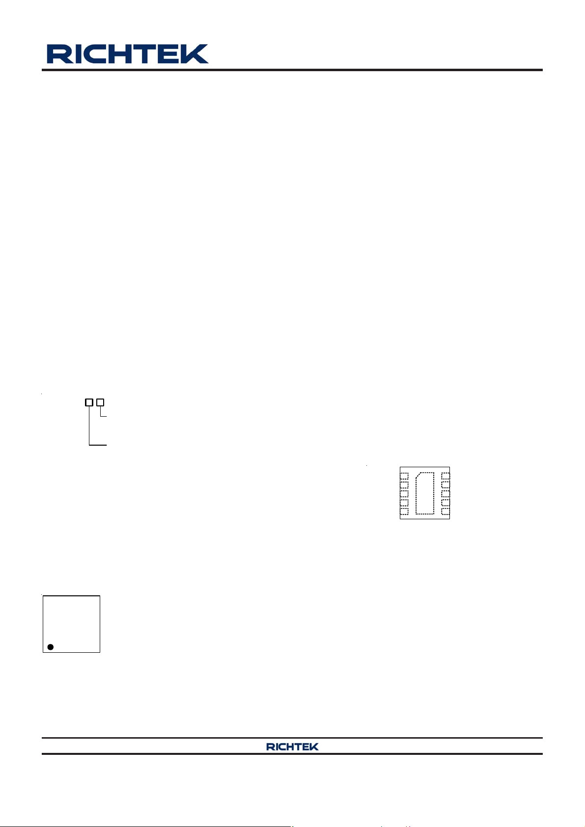
Pin Configurations
(TOP VIEW)
GND
11
10
PVIN
9
PVIN
8
SVIN
7
NC
6
FB
NC
LX
LX
PGOOD
EN
WDFN-10L 3x3
1
2
3
4
5
ΩΩ
Ω at V
ΩΩ
IN
Marking Information
11 : Product Code
11 YM
DNN
Copyright 2012 Richtek Technology Corporation. All rights reserved. is a registered trademark of Richtek Technology Corporation.
DS8061A-04 September 2012 www.richtek.com
©
YMDNN : Date Code
1
Page 2
RT8061A
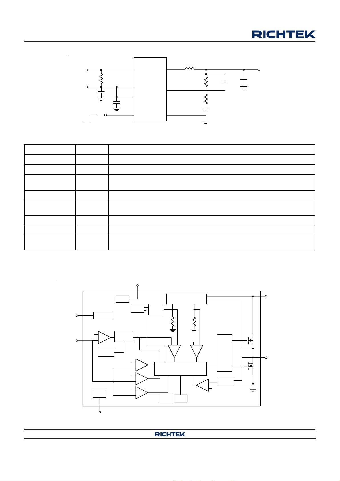
Typical Application Circuit
RT8061A
4
PGOOD
V
IN
Chip Enable
R1
PGOOD
9, 10
C1
8
5
PVIN
SVIN
EN
C
IN
LX
FB
11 (Exposed Pad)
GND
Functional Pin Description
Pin No. Pin Name Pin Function
1, 7 NC No Internal Connection.
2, 3 LX Switch Node. Connection this pin to the inductor.
2, 3
6
L
OUT
R
R
FB1
FB2
V
OUT
C
C
FF
OUT
4 PGOOD
Power Good Indicator. This pin is an open drain logic output that is pulled to
ground when the output voltage is less than 90% of the target output voltage.
5 EN Enable Control. Pull high to turn on. Do not float.
6 FB
Feed back . Th is pin rec eiv es the fe edb ac k vol tag e fro m a resi stiv e vo lta ge div id er
connected across the output.
8 SVIN Signal Input. Decouple this pin to GND with at least 1μF ceramic cap.
9, 10 PVIN Power Input. Decouple this pin to GND with at least 4.7μF ceramic cap.
11 (Exposed Pad) GND
The exposed pad must be soldered to a large PCB and connected to GND for
maximum power dissipation.
Function Block Diagram
0.6V
PGOOD
EN
PGOOD
FB
EN
Output
Clamp
EN
OSC
Slope
Com
ISEN
OC
Limit
PVIN
Int-SS
0.72V
OV
0.54V
POR
SVIN
Copyright 2012 Richtek Technology Corporation. All rights reserved. is a registered trademark of Richtek Technology Corporation.
©
0.4V
PGOOD
UV
Control
Logic
OTP
V
REF
Driver
LX
NISEN
Zero Current
DS8061A-04 September 2012www.richtek.com
2
Page 3
RT8061A
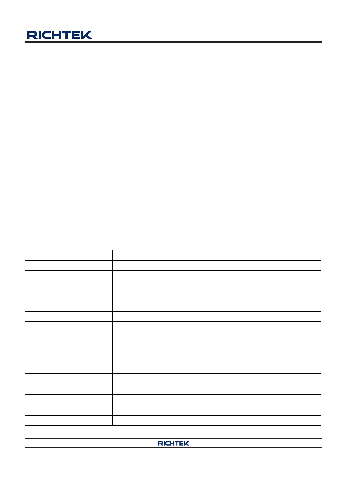
Absolute Maximum Ratings (Note 1)
z Supply Input V oltage, PVIN, SVIN-------------------------------------------------------------------------------- −0.3V to 6.5V
z LX Pin V oltage--------------------------------------------------------------------------------------------------------- (V
z Other I/O Pin Voltage------------------------------------------------------------------------------------------------ −0.3V to 6.5V
z Power Dissipation, P
@ TA = 25°C
D
WDNF-10L 3x3-------------------------------------------------------------------------------------------------------- 1.429W
z Package Thermal Resistance (Note 2)
W DFN-10L 3x3, θJA-------------------------------------------------------------------------------------------------- 70°C/W
WDFN-10L 3x3
z Junction T emperature------------------------------------------------------------------------------------------------ 150°C
z Lead Temperature (Soldering, 10 sec.)-------------------------------------------------------------------------- 260°C
z Storage T emperature Range --------------------------------------------------------------------------------------- −65°C to 150°C
z ESD Susceptibility (Note 3)
-------------------------------------------------------------------------------------------------- 8.2°C/W
θJC
HBM (Human Body Model)----------------------------------------------------------------------------------------- 2kV
Recommended Operating Conditions (Note 4)
0.3V) to 6.8V
IN +
z Supply Input V oltage, PVIN, SVIN--------------------------------------------------------------------------------
z Junction T emperature Range---------------------------------------------------------------------------------------
z Ambient T emperature Range---------------------------------------------------------------------------------------
2.7V to 5.5V
−40°C to 125°C
−40°C to 85°C
Electrical Characteristics
(VIN = 3.3V, T
Feedback Reference Voltage V
Feedback Leakage Current IFB -- 0.1 0.4 μA
DC Bias Current
Output Voltage Line Regulation V
Output Voltage Load Regulation I
Switch Leakage Current VEN = 0A -- -- 1 μA
Switching Frequency 0.8 1 1.2 MHz
Switch On Resistance, High R
Switch On Resistance, Low R
PMOS Current Lim it (latch-off) I
Under Voltage Lock out
Threshold
= 25°C, unless otherwise specified)
A
Parameter Symbol Test Conditions Min Typ Max Unit
0.594 0.6 0.606 V
REF
Active , V
0.7V, Not Switching -- 110 140
FB =
μA
Shutdown -- -- 1
2.7V to 5.5V I
IN =
= 0A to 3A −1 -- 1 %
OUT
DS(ON)_P
DS(ON)_N
LIM
V
V
4 -- -- A
5V -- 69 -- mΩ
IN =
5V -- 49 -- mΩ
IN =
= 0A -- 0.3 -- %/V
OUT
VIN Rising 2.2 2.4 2.6
V
UVLO
V
IN Falling 2 2.2 2.4
V
EN Threshold
Voltage
Logic-High VIH 1.6 -- -Logic-Low V
IL
-- -- 0.4
V
EN Pull Low Resistance -- 500 -- kΩ
Copyright 2012 Richtek Technology Corporation. All rights reserved. is a registered trademark of Richtek Technology Corporation.
DS8061A-04 September 2012 www.richtek.com
©
3
Page 4

RT8061A
Parameter Symbol Test Conditions Min Typ Max Unit
Ove r T emperature
Protection (latch-off)
Soft-Start Time tSS 500 -- -- μs
V
Discharge Resistance -- 1 00 -- Ω
OUT
V
Over Vol tage
OUT
Protection (latch-off, delay
time = 10μs)
V
Under Vol tage
OUT
Lockout Threshold
(latch-off)
Power Good Measured FB, With Respect to V
Power Good Hysteresis -- 5 -- %
Note 1. Stresses beyond those listed “Absolute Maximum Ratings” may cause permanent damage to the device. These are
stress ratings only, and functional operation of the device at these or any other conditions beyond those indicated in
the operational sections of the specifications is not implied. Exposure to absolute maximum rating conditions may
affect device reliability.
Note 2. θ
Note 3. Devices are ESD sensitive. Handling precaution is recommended.
Note 4. The device is not guaranteed to function outside its operating conditions.
is measured at T
JA
measured at the exposed pad of the package.
= 25°C on a high effective thermal conductivity four-layer test board per JEDEC 51-7. θJC is
A
-- 150 -- °C
T
SD
115 120 130 %
57 66 75 %
85 90 -- %
REF
Copyright 2012 Richtek Technology Corporation. All rights reserved. is a registered trademark of Richtek Technology Corporation.
4
©
DS8061A-04 September 2012www.richtek.com
Page 5

Typical Operating Characteristics
RT8061A
Efficiency vs. Load Current
100
98
96
V
V
IN
V
IN
= 4.2V
OUT
94
92
Efficiency (%)
90
88
86
00.511.522.53
Load Current (A)
Efficiency vs. Load Current
100
95
90
85
Eff iciency (%)
80
75
70
00.511.522.53
V
IN
Load Current (A)
= 3.3V
V
OUT
V
IN
= 1.05V
= 5V
= 3.3V
= 5V
Output Voltage (V)
Efficiency vs. Load Current
100
98
96
94
92
= 3.3V
V
V
OUT
90
88
Eff iciency (%)
86
84
82
80
00.511.522.53
V
IN
Load Current (A)
Output Voltage vs . Output Current
1.820
1.812
1.804
V
= 3.3V
1.796
1.788
1.780
0 0.6 1.2 1.8 2.4 3
Output Current (A)
IN
V
= 5V
IN
V
OUT
= 5V
IN
= 1.8V
= 1.8V
Current Limit vs. Input Voltage
7.0
6.5
6.0
5.5
5.0
4.5
Curr ent Limit (A)
4.0
3.5
V
= 1.05V
3.0
2.5 3 3.5 4 4.5 5 5.5
OUT
Input Voltage (V)
Copyright 2012 Richtek Technology Corporation. All rights reserved. is a registered trademark of Richtek Technology Corporation.
©
7.0
6.2
5.4
4.6
Curr ent Limit (A)
3.8
3.0
Current Limit vs. Temperature
V
= 5V
IN
V
= 3.3V
IN
V
= 1.05V
OUT
-50 -25 0 25 50 75 100 125
Temperatur e (°C)
DS8061A-04 September 2012 www.richtek.com
5
Page 6

RT8061A
90
79
Ω
68
(m )
57
DS(ON)
R
46
35
V
OUT
(50mV/Div)
R
-50 -25 0 25 50 75 100 125
vs. Temperature
DS(ON)
P-MOSFET
N-MOSFET
V
= 5V
IN
Temperatur e (°C)
Load Transient Response
V
OUT
(50mV/Div)
I
OUT
(2A/Div)
V
OUT
(5mV/Div)
Load Transient Response
VIN = 5V, V
Time (50μs/Div)
OUT
= 1.8V, I
= 0.5A to 3A
OUT
Switching
I
OUT
(2A/Div)
V
OUT
(5mV/Div)
V
LX
(500mV/Div)
I
LX
(2A/Div)
VIN = 5V, V
Time (50μs/Div)
Switching
VIN = 5V, V
OUT
= 1.8V, I
OUT
= 1.5A to 3A
OUT
= 1.8V, I
OUT
= 3A
V
LX
(500mV/Div)
I
LX
(1A/Div)
V
OUT
(1V/Div)
V
LX
(2V/Div)
VIN = 5V, V
= 1.8V, I
OUT
OUT
Time (500ns/Div)
Over Voltage Protection
VIN = 5V, V
= 1.8V, I
OUT
= 1.5A
= 1A
OUT
Time (500ns/Div)
Copyright 2012 Richtek Technology Corporation. All rights reserved. is a registered trademark of Richtek Technology Corporation.
©
Time (10μs/Div)
DS8061A-04 September 2012www.richtek.com
6
Page 7

RT8061A
V
OUT
(1V/Div)
V
LX
(2V/Div)
V
IN
(2V/Div)
Under Voltage Protection
VIN = 5V, V
Time (5μs/Div)
Power On from V
OUT
IN
= 1.8V
I
LX
(5A/Div)
V
OUT
(1V/Div)
V
LX
(5V/Div)
V
IN
(2V/Div)
Over Current Protection
VIN = 5V, V
Time (2.5μs/Div)
Power Off from V
OUT
IN
= 1.8V
V
OUT
(1V/Div)
I
LX
(2A/Div)
V
EN
(5V/Div)
V
OUT
(1V/Div)
I
LX
(2A/Div)
V
= 1.8V, I
OUT
Time (2.5ms/Div)
Power On from EN
VIN = 5V, V
= 1.8V, I
OUT
OUT
OUT
= 3A
= 3A
V
OUT
(1V/Div)
I
LX
(2A/Div)
V
EN
(5V/Div)
V
OUT
(1V/Div)
I
LX
(2A/Div)
V
= 1.8V, I
OUT
Time (2.5ms/Div)
Power Off from EN
VIN = 5V, V
= 1.8V, I
OUT
OUT
OUT
= 3A
= 3A
Time (200μs/Div)
Copyright 2012 Richtek Technology Corporation. All rights reserved. is a registered trademark of Richtek Technology Corporation.
©
Time (40μs/Div)
DS8061A-04 September 2012 www.richtek.com
7
Page 8

RT8061A
)
Application Information
The RT8061A is a single-phase buck PWM converter. It
provides single feedback loop, current mode control with
fast tra nsient response. An internal 0.6V reference allows
the output voltage to be precisely regulated for low output
voltage application s. A fixed switching frequency (1MHz)
oscillator and internal compensation are integrated to
minimize external component count. Protection features
include over current protection, under voltage protection,
over voltage protection and over temperature protection.
PWM Operation
The RT8061A utilizes DEM control to improve light load
efficiency. Depending on the load current, the controller
automatically operates in Diode-Emulation Mode (DEM)
or in Continuous Conduction Mode (CCM) with fixedfrequency PWM.
At light load condition, the RT8061A automatically operates
in diode-emulation mode to reduce switching frequency
and improve efficiency. As the output current decreases
from heavy load condition, the inductor current is also
reduced and eventually comes to the point where its valley
touches zero current, which is the boundary between
continuous conduction and discontinuous conduction
modes. By emulating the behavior of diodes, the low side
MOSFET allows only partial negative current to flow when
the inductor freewheeling current reaches negative. As the
load current further decrea ses, it tak es longer and longer
to discharge the output capacitor to the level that that
requires the next UGA TE “ON” cycle. In contrast, when
the output current increa ses from light load to heavy load,
the switching frequency increa ses to the preset value a s
the inductor current reaches the continuous conduction.
The controller will then operate in continuous conduction
mode with 1MHz fixed PWM switching frequency .
Output Voltage Setting
Connect a resistive voltage divider at the FB between V
and GND to adjust the output voltage. The output voltage
is set according to the following equation :
R1
⎛⎞
V= V 1+
OUT FB
×
⎜⎟
R2
⎝⎠
where VFB is 0.6V (typ.).
OUT
V
OUT
R1
FB
R2
GND
Figure 1. Setting V
with a V oltage Divider
OUT
Chip Enable and Disable
The EN pin allows for power sequencing between the
controller bias voltage and another voltage rail. The
RT8061A remains in shutdown if the EN pin is lower tha n
400mV. When the EN pin rises above the VEN trip point,
the RT8061A begins a new initialization and soft-start cycle.
Internal Soft-Start
The RT8061A provides an internal soft-start function to
prevent large inrush current and output voltage overshoot
when the converter starts up. The Soft-Start (SS)
automatically begins once the chip is enabled. During softstart, the internal soft-start capacitor becomes charged
and generates a linear ramping up voltage across the
cap a citor. This voltage clamps the voltage at the FB pin,
causing PWM pulse width to increa se slowly and in turn
reduce the output surge current. The internal 0.6V
reference takes over the loop control once the internal
ramping-up voltage becomes higher tha n 0.6V .
UVLO Protection
The RT8061A ha s input U nder V oltage Lockout protection
(UVLO). If the input voltage exceeds the UVLO rising
threshold voltage (2.4V typ.), the converter resets and
prepares the PWM for operation. If the input voltage falls
below the UVLO falling threshold voltage during normal
operation, the device will stop switching. The UVLO rising
and falling threshold voltage has a hysteresis to prevent
noise-caused reset.
Inductor Selection
The switching frequency (on-time) and operating point (%
ripple or LIR) determine the inductor value as shown below :
VVV
×−
(
L =
OUT IN OUT
fLIRI V
×× ×
SW LOAD(MAX) IN
Copyright 2012 Richtek Technology Corporation. All rights reserved. is a registered trademark of Richtek Technology Corporation.
8
©
DS8061A-04 September 2012www.richtek.com
Page 9

RT8061A
where LIR is the ratio of the peak-to-pea k ripple current to
the average inductor current.
Find a low loss inductor having the lowest possible DC
resistance that fits in the allotted di mensions. Ferrite cores
are often the best choice, although powdered iron is
inexpensive and ca n work well at 200kHz. The core must
be large enough not to saturate at the peak inductor current
(I
) :
PEAK
LIR
⎛⎞
I = I I
PEAK LOAD(MAX) LOAD(MAX)
+×
⎜⎟
2
⎝⎠
The calculation above serves a s a general reference. To
further improve transient response, the output inductor
can be further reduced. This relation should be considered
along with the selection of the output cap a citor.
Input Capacitor Selection
High quality ceramic in put decoupling capacitor, such as
X5R or X7R, with values greater than 20μF are
recommended for the input ca pa citor. The X5R and X7R
ceramic ca pa citors are usually selected for power regulator
capacitors because the dielectric material has less
cap acita nce variation and more temperature stability .
V oltage rating a nd current rating are the key parameters
when selecting an input ca pa citor. Generally , selecting a n
input ca pa citor with voltage rating 1.5 ti mes greater tha n
the maximum input voltage is a conservatively safe design.
The input capacitor is used to supply the input RMS
current, which can be a pproximately calculated using the
following equation :
II 1
IN_RMS LOAD
=× ×−
VV
⎛⎞
OUT OUT
⎜⎟
VV
IN IN
⎝⎠
The next step is selecting a proper capacitor for RMS
current rating. One good design is using more than one
ca pacitor with low Equivalent Series Resistance (ESR) in
parallel to form a ca pa citor bank.
The input capacitance value determines the input ripple
voltage of the regulator. The input voltage ripple can be
a pproximately calculated using the f ollowing equation :
I0.25
V
IN
OUT(MAX)
Cf
Δ=
For example, if I
×
×
IN SW
OUT(MAX)
= 3A, CIN = 20μF, fSW = 1MHz,
the input voltage ripple will be 37.5mV.
Output Capacitor Selection
The output capacitor and the inductor form a low pass
filter in the buck topology. In steady state condition, the
ripple current flowing into/out of the capacitor results in
ripple voltage. The output voltage ripple (V
) can be
P-P
calculated by the following equation :
=× × +
V LIR I ESR
P-P LOAD(MAX)
⎛⎞
⎜⎟
⎝⎠
8C f
1
××
OUT SW
When load tran sient occurs, the output capa citor supplies
the load current before the controller can respond.
Therefore, the ESR will dominate the output voltage sag
during load tran sient. The output voltage undershoot (V
SAG
can be calculated by the following equation :
=Δ ×
VIESR
SAG LOAD
For a given output voltage sag specification, the ESR value
can be determined.
Another parameter that ha s influence on the output voltage
sag is the equivalent series inductance (ESL). The rapid
change in load current results in di/dt during transient.
Therefore, the ESL contributes to part of the voltage sag.
Using a capa citor with low ESL ca n obtain better transient
performance. Generally, using several capacitors
connected in parallel can have better tra nsient performance
than using a single capacitor for the sa me total ESR.
Unlike the electrolytic ca pa citor, the cera mic ca pacitor ha s
relatively low ESR and ca n reduce the voltage deviation
during load transient. However , the cera mic ca pacitor ca n
only provide low capa citance value. Theref ore, use a mixed
combination of electrolytic ca pacitor and cera mic ca pa citor
to obtain better transient performa nce.
Power Good Output (PGOOD)
PGOOD is a n open-drain type output and requires a pullup resistor. PGOOD is actively held low in soft-start,
standby, and shutdown. It is released when the output
voltage rises above 90% of nominal regulation point. The
PGOOD signal goes low if the output is turned off or is
10% below its nominal regulation point.
)
Copyright 2012 Richtek Technology Corporation. All rights reserved. is a registered trademark of Richtek Technology Corporation.
DS8061A-04 September 2012 www.richtek.com
©
9
Page 10

RT8061A
Under Voltage Protection (UVP)
The output voltage can be continuously monitored for under
voltage. When under voltage protection is enabled, both
UGA TE and LGATE gate drivers will be forced low if the
output is less than 66% of its set voltage threshold. The
UVP will be ignored for at lea st 3ms (typ.) after start up or
a rising edge on the EN threshold. T oggle EN threshold or
cycle VIN to reset the UVP fault latch and restart the
controller.
Over Voltage Protection (OVP)
The RT8061A is latched once OVP is triggered and ca n
only be relea sed by toggling EN threshold or cycling VIN.
There is a 10μs delay built into the over voltage protection
circuit to prevent false transition.
Over Current Protection (OCP)
The RT8061A provides over current protection by detecting
high side MOSFET peak inductor current. If the sensed
peak inductor current remains over 4A (typ) for 5 clock
cycles, OCP will be triggered. When OCP trips, the
RT8061A will shut down and enter Latch-Off Mode to stop
the energy transfer to the load. In Latch-Off Mode, the
RT8061A can only be reset by EN or VIN.
Thermal Shutdown (OTP)
The device implements internal thermal shutdown when
the junction temperature exceeds 150°C. When the OTP
function is triggered, the RT8061A shuts down a nd enters
Latch-Off Mode. In Latch-Off Mode, the RT8061A can be
reset by EN or VIN.
where T
the ambient temperature, a nd θ
is the maximum junction temperature, T
J(MAX)
is the junction to ambient
JA
A
thermal resistance.
For recommended operating condition specifications, the
maximum junction temperature is 125°C. The junction to
a mbient thermal resistance, θJA, is layout dependent. For
W DFN-10L 3x3 packages, the thermal resista nce, θJA, is
70°C/W on a standard JEDEC 51-7 f our-layer thermal test
board. The maximum power dissipation at TA = 25°C can
be calculated by the following formula :
P
= (125°C − 25°C) / (70°C/W) = 1.429W for
D(MAX)
W DF N-10L 3x3 pa ckage
The maximum power dissipation depends on the operating
ambient temperature for fixed T
and thermal
J(MAX)
resistance, θJA. The derating curve in Figure 2 allows the
designer to see the effect of rising ambient temperature
on the maximum power dissipation.
1.6
1.4
1.2
1.0
0.8
0.6
0.4
0.2
Maximum Power Dissipation (W) 1
0.0
0 25 50 75 100 125
Ambient Temperature ( °C)
Four-Layer PCB
is
Thermal Considerations
Figure 2. Derating Curve of Maxi mum Power Dissi pation
For continuous operation, do not exceed absolute
maximum junction temperature. The maximum power
dissipation depends on the thermal resistance of the IC
package, PCB layout, rate of surrounding airflow, and
difference between junction and a mbient temperature. The
maximum power dissipation can be calculated by the
following formula :
P
Copyright 2012 Richtek Technology Corporation. All rights reserved. is a registered trademark of Richtek Technology Corporation.
10
D(MAX)
= (T
©
J(MAX)
− TA) / θ
JA
DS8061A-04 September 2012www.richtek.com
Page 11

RT8061A
Layout Considerations
Layout is very important in high frequency switching
converter design. The PCB can ra diate excessive noise
and contribute to converter insta bility with improper layout.
Certain points must be considered before starting a layout
using the RT8061A.
` Make the tra ces of the main current paths a s short a nd
wide as possible.
` Put the input capa citor a s close a s possible to the device
pins (VIN and GND).
` LX node encounters high frequency voltage swings so
it should be kept in a small area. Keep sensitive
components away from the LX node to prevent stray
cap acitive noise pick-up.
` Ensure all feedback network connections are short a nd
direct. Place the feedba ck network a s close to the chi p
as possible.
` The GND pin a nd Exposed Pad should be connected to
a strong ground plane for heat sinking and noise
protection.
The output capacitor must
be placed near the IC.
C
OUT
V
OUT
R
PGOOD
V
IN
R
EN
LX should be connected to inductor by
wide and short trace. Keep sensitive
components away from this trace.
NC
LX
LX
PGOOD
EN
Input capacitor must be placed
as close to the IC as possible.
GND
1
2
3
GND
4
11
5
Figure 3. PCB Layout Guide
C
10
PVIN
9
PVIN
8
SVIN
7
NC
6
FB
The voltage divider must
be connected as close to
the device as possible.
IN1
R1
C
IN2
R2
V
OUT
` An example of PCB layout guide is shown in Figure 3.
for reference.
Copyright 2012 Richtek Technology Corporation. All rights reserved. is a registered trademark of Richtek Technology Corporation.
©
DS8061A-04 September 2012 www.richtek.com
11
Page 12

RT8061A
Outline Dimension
D
D2
L
E
e
A
A3
A1
1
b
E2
SEE DETAIL A
2
1
DETAIL A
1
2
Pin #1 ID a nd T ie Bar Mark Option s
Note : The configuration of the Pin #1 identifier is optional,
but must be located within the zone indicated.
Dimensions In Millimeters Dimensions In Inches
Symbol
Min Max Min Max
A 0.700 0.800 0.028 0.031
A1 0.000 0.050 0.000 0.002
A3 0.175 0.250 0.007 0.010
b 0.180 0.300 0.007 0.012
D 2.950 3.050 0.116 0.120
D2 2.300 2.650 0.091 0.104
E 2.950 3.050 0.116 0.120
E2 1.500 1.750 0.059 0.069
e 0.500 0.020
L 0.350 0.450
W-Type 10L DFN 3x3 Package
0.014 0.018
Richtek Technology Corporation
5F, No. 20, Taiyuen Street, Chupei City
Hsinchu, Taiwan, R.O.C.
Tel: (8863)5526789
Richtek products are sold by description only. Richtek reserves the right to change the circuitry and/or specifications without notice at any time. Customers should
obtain the latest relevant information and data sheets before placing orders and should verify that such information is current and complete. Richtek cannot
assume responsibility for use of any circuitry other than circuitry entirely embodied in a Richtek product. Information furnished by Richtek is believed to be
accurate and reliable. However, no responsibility is assumed by Richtek or its subsidiaries for its use; nor for any infringements of patents or other rights of third
parties which may result from its use. No license is granted by implication or otherwise under any patent or patent rights of Richtek or its subsidiaries.
DS8061A-04 September 2012www.richtek.com
12
Page 13

 Loading...