

Page 1
RT7297B
®
DS7297B-02 September 2012 www.richtek.com
1
©
Copyright 2012 Richtek Technology Corporation. All rights reserved. is a registered trademark of Richtek Technology Corporation.
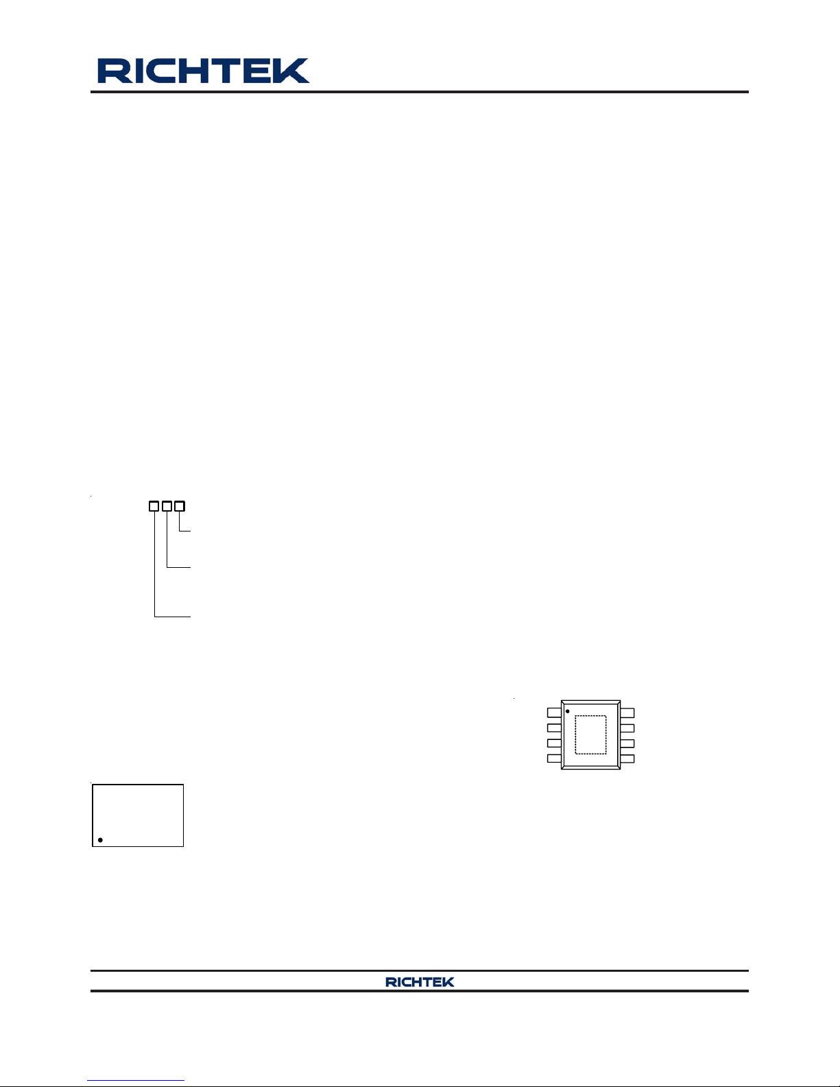
Ordering Information
Note :
Richtek products are :
` RoHS compliant and compatible with the current require-
ments of IPC/JEDEC J-STD-020.
` Suitable for use in SnPb or Pb-free soldering processes.
Pin Configurations
(TOP VIEW)
Applications
Wireless AP/Router
Set-Top-Box
Industrial and Commerci al Low Power Systems
LCD Monitors a nd TVs
Green Electronics/Appliances
Point of Load Regulation of High-Performance DSPs
SOP-8 (Exposed Pad)
3A, 18V, 1.2MHz Synchronous Step-Down Converter
General Description
The RT7297B is a high efficiency , monolithic synchronous
step-down DC/DC converter that can deliver up to 3A
output current from a 4.5V to 18V input supply. The
RT7297B's current mode architecture and external
compensation allow the transient response to be
optimized over a wide input voltage range a nd loads. Cycleby-cycle current limit provides protection against shorted
outputs, and soft-start eliminate s input current surge during
start-up. The RT7297B also provides under voltage
protection and thermal shutdown protection. The low
current (<3μA) shutdown mode provides output
disconnection, enabling easy power management in
battery-powered systems. The RT7297B is available in
an SOP-8 (Exposed Pad) pa ckage.
Features
±±
±±
±1.5% High Accuracy Reference Voltage
4.5V to 18V Input Voltage Range
3A Output Current
Integrated N-MOSFET Switches
Current Mode Control
Fixed Frequency Operation : 1.2MHz
Output Adjustable from 0.8V to 12V
Up to 95% Efficiency
Programmable Soft-Start
Stable with Low ESR Ceramic Output Capacitors
Cycle-by-Cycle Over Current Protection
Input Under Voltage Lockout
Output Under Voltage Protection
Thermal Shutdown Protection
RoHS Compliant and Halogen Free
BOOT
VIN
SW
GND
SS
EN
FB
COMP
GND
2
3
4
5
6
7
8
9
Package Type
SP : SOP-8 (Exposed Pad-Option 1)
RT7297B
Lead Plating System
Z : ECO (Ecological Element with
Halogen Free and Pb free)
H : UVP Hiccup
L : UVP Latch-Off
Marking Information
RT7297BxZSP : Product Number
x : H or L
YMDNN : Date Code
RT7297Bx
ZSPYMDNN
Page 2
RT7297B
2
DS7297B-02 September 2012www.richtek.com
©
Copyright 2012 Richtek Technology Corporation. All rights reserved. is a registered trademark of Richtek Technology Corporation.
Functional Pin Description
Pin No. Pin Name Pin Function
1 BOOT
Bootstrap for High Side Gate Driver. Connect a 0.1μF or greater ceramic
capacitor from BOOT to SW pins.
2 VIN
Input Supply Voltage, 4.5V to 18V. Must bypass with a suitable large ceramic
capacitor.
3 SW Switch Node. Connect this pin to an external L-C filter.
4,
9 (Exposed Pad)
GND
Ground. The exposed pad must be soldered to a large PCB and connected to
GND for maximum power dissipation.
5 FB
Feedback Input. It is used to regulate the output of the converter to a set value
via an external resistive voltage divider.
6 COMP
Compensation Node. COMP is used to compensate the regulation control
loop. Connect a series RC network from COMP to GND. In some cases, an
additional capacitor from COMP to GND is required.
7 EN
Enable Input Pin. A logic high enables the converter; a logic low forces the IC
into shutdown mode reducing the supply current to less than 3μA. Attach this
pin to VIN with a 100kΩ pull up resistor for automatic startup.
8 SS
Soft-Start Control Input. SS controls the soft-start period. Connect a capacitor
from SS to GND to set the soft-start period. A 0.1μF capacitor sets the
soft-start period to 13.5ms.
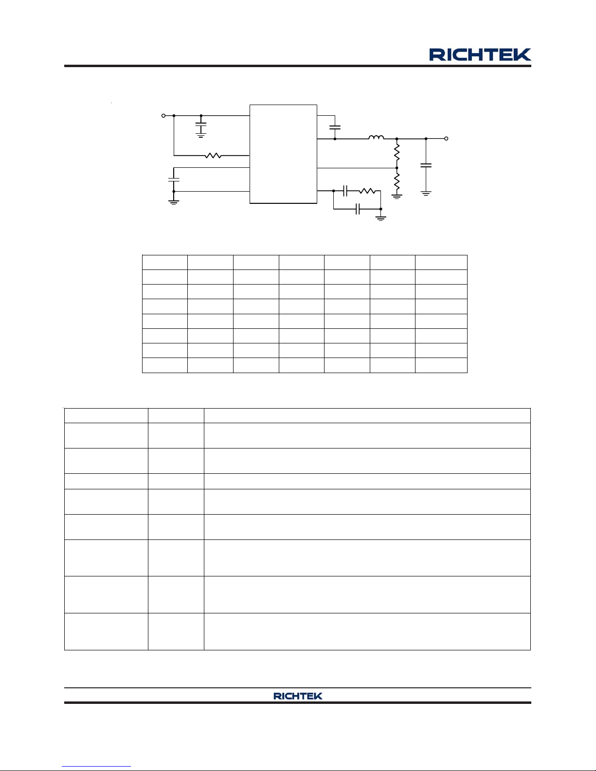
Typical Application Circuit
V
OUT
(V) R1 (kΩ) R2 (kΩ) RC (kΩ) CC (nF) L (μH) C
OUT
(μF)
8 27 3 51 2.2 10 22 x 2
5 62 1 1.8 33 2.2 6.8 22 x 2
3.3 75 24 22 2.2 3.6 22 x 2
2.5 25.5 12 16 2.2 3.6 22 x 2
1.5 10.5 12 10 2.2 2 22 x 2
1.2 12 24 8.2 2.2 2 22 x 2
1 3 12 6.8 2.2 2 22 x 2
Table 1. Suggested Components Selection
VIN
EN
GND
BOOT
FB
SW
7
5
2
3
1
L
3.6µH
0.1µF
22µF x 2
R1
75k
R2
24k
V
OUT
3.3V
10µF x 2
V
IN
4.5V to 18V
RT7297B
SS
8
C
SS
COMP
C
C
2.2nF
R
C
22k
C
P
Open
6
4, 9 (Exposed Pad)
C
BOOT
C
IN
0.1µF
C
OUT
R
EN
100k
Page 3
RT7297B
3
DS7297B-02 September 2012 www.richtek.com
©
Copyright 2012 Richtek Technology Corporation. All rights reserved. is a registered trademark of Richtek Technology Corporation.
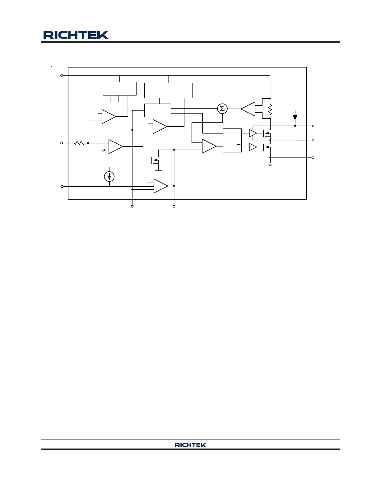
Function Block Diagram
+
-
+
-
+
-
UV
Comparator
Oscillator
Foldback
Control
0.4V
Internal
Regulator
+
-
Shutdown
Comparator
Current Sense
Amplifier
BOOT
VIN
GND
SW
FB
EN
COMP
V
CC
6µA
Slope Comp
Current
Comparator
+
-
EA
0.8V
SRQ
Q
SS
+
-
1.2V
Lockout
Comparator
V
CC
+
Ω90m
Ω110m
V
A
2.5V
V
A
R
SENSE
5kΩ
Page 4
RT7297B
4
DS7297B-02 September 2012www.richtek.com
©
Copyright 2012 Richtek Technology Corporation. All rights reserved. is a registered trademark of Richtek Technology Corporation.
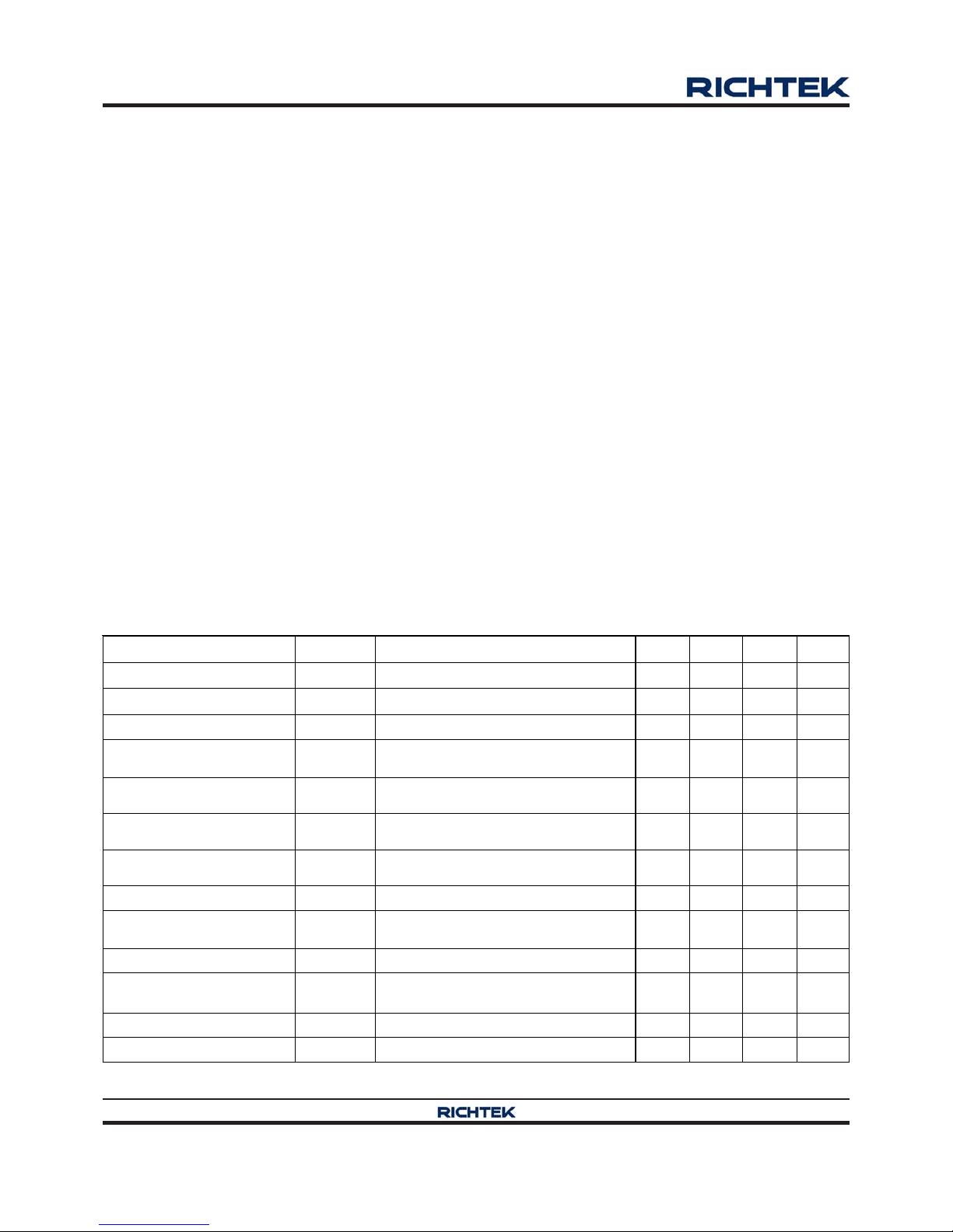
Electrical Characteristics
(V
IN
= 12V, TA = 25°C, unless otherwise specified)
Absolute Maximum Ratings (Note 1)
Supply Input V oltage, VIN ----------------------------------------------------------------------------------------- −0.3V to 20V
Switch Voltage, SW ------------------------------------------------------------------------------------------------ −0.3V to (V
IN
+ 0.3V)
V
BOOT
− VSW---------------------------------------------------------------------------------------------------------- −0.3V to 6V
Other Pins Voltage -------------------------------------------------------------------------------------------------- −0.3V to 20V
Power Dissipation, P
D
@ T
A
= 25°C
SOP-8 (Exposed Pad) --------------------------------------------------------------------------------------------- 1.333W
Pa ck age Thermal Resista nce (Note 2)
SOP-8 (Exposed Pad), θJA---------------------------------------------------------------------------------------- 75°C/W
SOP-8 (Exposed Pad), θJC--------------------------------------------------------------------------------------- 15°C/W
Lead Temperature (Soldering, 10 sec.)------------------------------------------------------------------------- 260°C
Junction T emperature----------------------------------------------------------------------------------------------- 150°C
Storage T emperature Range -------------------------------------------------------------------------------------- −65°C to 150°C
ESD Susceptibility (Note 3)
HBM (Human Body Model)---------------------------------------------------------------------------------------- 2kV
Recommended Operating Conditions (Note 4)
Supply Input V oltage, VIN ----------------------------------------------------------------------------------------- 4.5V to 18V
Junction T emperature Range-------------------------------------------------------------------------------------- − 40°C to 125°C
Ambient T emperature Range-------------------------------------------------------------------------------------- − 40°C to 85°C
Parameter Symbol Test Conditions Min Typ Max Unit
Shutdown Supply Current V
EN
= 0V -- 0.5 3 μA
Supply Current V
EN
= 3V, VFB = 0.9V -- 0.8 1.2 mA
Reference Voltage V
REF
4.5V ≤ VIN ≤ 18V 0.788 0.8 0.812 V
Error Amplifier
Transconductance
G
EA
ΔIC = ±10μA -- 940 -- μA/V
High Side Switch
On-Resistance
R
DS(ON)1
-- 110 -- mΩ
Low Side Switch
On-Resistance
R
DS(ON)2
-- 90 -- mΩ
High Side Switch Leakage
Current
V
EN
= 0V, VSW = 0V -- 0 10 μA
Upper Switch Current Limit Min. Duty Cycle, V
BOOT
− VSW = 4.8V -- 5.1 -- A
COMP to Current Sense
Transconductance
G
CS
-- 4.7 -- A/V
Oscillation Frequency f
OSC1
1 1.2 1.4 MHz
Short Circuit Oscillation
Frequency
f
OSC2
VFB = 0V -- 270 -- kHz
Maximum Duty Cycle D
MAX
VFB = 0.7V -- 78 -- %
Minimum On Time tON -- 100 -- ns
Page 5
RT7297B
5
DS7297B-02 September 2012 www.richtek.com
©
Copyright 2012 Richtek Technology Corporation. All rights reserved. is a registered trademark of Richtek Technology Corporation.
Parameter Symbol Test Conditions Min Typ Max Unit
Logic-High VIH 2.7 -- 18
EN Input Threshold
Voltage
Logic-Low V
IL
-- -- 0.4
V
Input Under Volt age Lockout
Threshold
V
UVLO
VIN Rising 3.8 4.2 4.5 V
Input Under Volt age Lockout
Hysteresis
ΔV
UVLO
-- 320 -- mV
Soft-Start Current ISS V
SS
= 0V -- 6 -- μA
Soft-Start Period tSS C
SS
= 0.1μF -- 13.5 -- ms
Thermal Shutdown TSD -- 150 -- °C
Note 1. Stresses beyond those listed “Absolute Maximum Ratings” may cause permanent damage to the device. These are
stress ratings only, and functional operation of the device at these or any other conditions beyond those indicated in
the operational sections of the specifications is not implied. Exposure to absolute maximum rating conditions may
affect device reliability.
Note 2. θ
JA
is measured at T
A
= 25°C on a high effective thermal conductivity four-layer test board per JEDEC 51-7. θJC is
measured at the exposed pad of the package.
Note 3. Devices are ESD sensitive. Handling precaution is recommended.
Note 4. The device is not guaranteed to function outside its operating conditions.
Page 6

RT7297B
6
DS7297B-02 September 2012www.richtek.com
©
Copyright 2012 Richtek Technology Corporation. All rights reserved. is a registered trademark of Richtek Technology Corporation.
Typical Operating Characteristics
Efficiency vs. Load Current
0
10
20
30
40
50
60
70
80
90
100
00.511.522.53
Load Curren t (A)
Eff iciency (%)
V
OUT
= 3.3V
V
IN
= 12V
V
IN
= 17V
Output Voltage vs. Temperature
3.26
3.27
3.28
3.29
3.30
3.31
3.32
3.33
3.34
-50 -25 0 25 50 75 100 125
Temperature (°C)
Output Voltage ( V )
V
IN
= 12V, V
OUT
= 3.3V
Output Voltage vs. Load Current
3.20
3.22
3.24
3.26
3.28
3.30
3.32
3.34
3.36
3.38
3.40
0 0.5 1 1.5 2 2.5 3
Load Current (A)
Output V oltage (V)
V
OUT
= 3.3V
V
IN
= 12V
V
IN
= 17V
Switching Frequency vs. Temperature
1.10
1.11
1.12
1.13
1.14
1.15
1.16
1.17
1.18
1.19
1.20
1.21
1.22
1.23
1.24
-50 -25 0 25 50 75 100 125
Temperature (°C)
Swit ching Frequency (kHz) 1
V
OUT
= 3.3V, I
OUT
= 0A
V
IN
= 17V
V
IN
= 12V
Switching Freq uency vs . Input Voltage
1.16
1.17
1.18
1.19
1.20
1.21
1.22
1.23
1.24
1.25
1.26
4.5 7 9.5 12 14.5 17
Input Vol tag e (V)
Swit ching Frequency (MHz) 1
V
IN
= 4.5V to 17V, V
OUT
= 3.3V, I
OUT
= 0A
Output Voltage vs . Input Voltage
3.26
3.27
3.28
3.29
3.30
3.31
3.32
3.33
3.34
4 6 81012141618
Inpu t Volt age (V)
Output Voltage ( V )
V
IN
= 4.5V to 17V
Page 7

RT7297B
7
DS7297B-02 September 2012 www.richtek.com
©
Copyright 2012 Richtek Technology Corporation. All rights reserved. is a registered trademark of Richtek Technology Corporation.
Current Limit vs. Temperature
3.0
3.5
4.0
4.5
5.0
5.5
6.0
6.5
7.0
-50-25 0 25 50 75100125
Temperature (°C)
Current Li m it ( A )
V
IN
= 12V, V
OUT
= 3.3V
Current Limit vs. Input Voltage
1.0
1.5
2.0
2.5
3.0
3.5
4.0
4.5
5.0
5.5
6.0
4.5 7 9.5 12 14.5 17
Input Vol tag e (V)
Current Li m it ( A )
V
IN
= 4.5V to 17V, V
OUT
= 3.3V
Time (100μs/Div)
Load Transient Response
V
OUT
(100mV/Div)
I
OUT
(2A/Div)
V
IN
= 12V, V
OUT
= 3.3V, I
OUT
= 0A to 3A
Time (100μs/Div)
Load Transient Response
V
OUT
(100mV/Div)
I
OUT
(2A/Div)
V
IN
= 12V, V
OUT
= 3.3V, I
OUT
= 1.5A to 3A
Time (500ns/Div)
Switching
V
SW
(10V/Div)
V
OUT
(5mV/Div)
I
L
(2A/Div)
V
IN
= 12V , V
OUT
= 3.3V, I
OUT
= 1.5A
Time (500ns/Div)
Switching
V
IN
= 12V, V
OUT
= 3.3V, I
OUT
= 3A
V
SW
(10V/Div)
V
OUT
(5mV/Div)
I
L
(2A/Div)
Page 8

RT7297B
8
DS7297B-02 September 2012www.richtek.com
©
Copyright 2012 Richtek Technology Corporation. All rights reserved. is a registered trademark of Richtek Technology Corporation.
Power On from V
IN
Time (10ms/Div)
VIN = 12V, V
OUT
= 3.3V, I
OUT
= 3A
I
L
(2A/Div)
V
OUT
(2V/Div)
V
IN
(5V/Div)
Power Off from V
IN
Time (10ms/Div)
I
L
(2A/Div)
V
OUT
(2V/Div)
V
IN
(5V/Div)
VIN = 12V, V
OUT
= 3.3V, I
OUT
= 3A
Power On from EN
Time (10ms/Div)
V
OUT
(2V/Div)
V
EN
(5V/Div)
I
L
(2A/Div)
VIN = 12V, V
OUT
= 3.3V, I
OUT
= 3A
Power Off from EN
Time (10ms/Div)
VIN = 12V, V
OUT
= 3.3V, I
OUT
= 3A
V
OUT
(2V/Div)
V
EN
(5V/Div)
I
L
(2A/Div)
Page 9

RT7297B
9
DS7297B-02 September 2012 www.richtek.com
©
Copyright 2012 Richtek Technology Corporation. All rights reserved. is a registered trademark of Richtek Technology Corporation.
Application Information
Output Voltage Setting
The resistive divider allows the FB pin to sense the output
voltage as shown in Figure 1.
Figure 1. Output Voltage Setting
The output voltage is set by an external resistive voltage
divider according to the following equation :
OUT REF
R1
V = V 1
R2
⎛⎞
+
⎜⎟
⎝⎠
Where V
REF
is the reference voltage (0.8V typ.).
External Bootstrap Diode
Connect a 100nF low ESR ceramic capacitor between
the BOOT pin and SW pin. This capacitor provides the
gate driver voltage for the high side MOSFET.
It is recommended to add an external bootstrap diode
between an external 5V and BOOT pin for efficiency
improvement when input voltage is lower than 5.5V or duty
ratio is higher than 65% .The bootstrap diode can be a
low cost one such as IN4148 or BAT54. The external 5V
can be a 5V fixed in put from system or a 5V output of the
RT7297B. Note that the external boot voltage must be
lower than 5.5V
Figure 2. External Bootstrap Diode
Chip Enable Operation
The EN pin is the chip enable input. Pulling the EN pin
low (<0.4V) will shutdown the device. During shutdown
mode, the RT7297B quiescent current drops to lower than
3μA. Driving the EN pin high (>2.7V, <18V) will turn on
the device again. For external timing control, the EN pin
can also be externally pulled high by adding a REN resistor
and CEN capa citor from the VIN pin (see Figure 3).
SW
BOOT
5V
RT7297B
0.1µF
RT7297B
GND
FB
R1
R2
V
OUT
Soft-Start
The RT7297B provides soft-start function. The soft-start
function is used to prevent large inrush current while
converter is being powered-up. The soft-start timing ca n
be programmed by the extern al capa citor between SS and
GND. An internal current source I
SS
(6μA) charges an
external cap acitor to build a soft-start ra mp voltage. The
VFB voltage will track the internal ra mp voltage during softstart interval. The typical soft-start time is calculated as
follows :
RT7297B
EN
GND
V
IN
R
EN
C
EN
EN
An external MOSFET can be a dded to implement digital
control on the EN pin when no system voltage above 1.8V
is available, a s shown in Figure 4. In this case, a 100kΩ
pull-up resistor, REN, is connected between VIN and the
EN pin. MOSFET Q1 will be under logic control to pull
down the EN pin.
RT7297B
EN
GND
100k
V
IN
R
EN
Q1
EN
Figure 3. Enable Timing Control
Figure 4. Digital Ena ble Control Circuit
SS
SS SS
SS
0.8 C
Soft-Start time t = , if C capacitor
I
0.8 0.1
is 0.1 F, then soft-start time = 13.5ms
6
μ
μ
μ
×
×
≒
Page 10

RT7297B
10
DS7297B-02 September 2012www.richtek.com
©
Copyright 2012 Richtek Technology Corporation. All rights reserved. is a registered trademark of Richtek Technology Corporation.
OUT OUT
L
IN
VV
I = 1
fL V
⎡⎤⎡ ⎤
Δ×−
⎢⎥⎢ ⎥
×
⎣⎦⎣ ⎦
Under Voltage Protection
Hiccup Mode
For the RT7297BH, it provides Hiccup Mode Under V oltage
Protection (UVP). When the VFB voltage drops below
0.4V, the UVP function will be triggered to shut down
switching operation. If the UVP condition remains for a
period, the RT7297BH will retry automatically . When the
UVP condition is removed, the converter will resume
operation. The UVP is disabled during Soft-Start period.
Having a lower ripple current reduces not only the ESR
losses in the output capa citors but also the output voltage
ripple. High frequency with small ripple current ca n achieve
the highest efficiency operation. However, it requires a
large inductor to achieve this goal.
For the ripple current selection, the value of ΔI
L
= 0.24(I
MAX
)
will be a reasonable starting point. The largest ripple
current occurs at the highest VIN. To guarantee that the
ripple current stays below the specified maximum, the
inductor value should be chosen according to the following
equation :
Table 2. Suggested Inductors for Typical
Application Circuit
Component
Supplier
Series
Dimensions
(mm)
TDK VLF10045 10 x 9.7 x 4.5
TDK SLF12565 12.5 x 12.5 x 6.5
TAIYO
YUDEN
NR 8040 8 x 8 x 4
OUT OUT
L(MAX) IN(MAX)
VV
L = 1
fI V
⎡⎤⎡ ⎤
×−
⎢⎥⎢ ⎥
×Δ
⎣⎦⎣ ⎦
The inductor's current rating (caused a 40°C temperature
rising from 25°C ambient) should be greater than the
maximum load current and its saturation current should
be greater than the short circuit pea k current limit. Plea se
see Table 2 for the inductor selection reference.
Figure 5. Hiccup Mode Under Voltage Protection
Figure 6. Latch-Off Mode Under Voltage Protection
Latch-Off Mode
For the RT7297BL, it provides Latch-Off Mode Under
Voltage Protection (UVP). When the FB voltage drops
below half of the feedback reference voltage, VFB, UVP
will be triggered and the RT7297BL will shutdown in LatchOff Mode. In shutdown condition, the RT7297BL can be
reset by EN pin or power input VIN.
Over Temperature Protection
The RT7297B features an Over Temperature Protection
(OTP) circuitry to prevent from overheating due to
excessive power dissipation. The OTP will shut down
switching operation when junction temperature exceeds
150°C. Once the junction temperature cools down by
approxi mately 20°C, the converter will resume operation.
T o maintain continuous operation, the maximum junction
temperature should be lower than 125°C.
Inductor Selection
The inductor value and operating frequency determine the
ripple current according to a specific input and output
voltage. The ripple current ΔI
L
increases with higher V
IN
and decrea ses with higher inducta nce.
Time (50ms/Div)
Hiccup Mode
V
OUT
(2V/Div)
I
LX
(2A/Div)
I
OUT
= Short
Time (250μs/Div)
Latch-Off Mode
V
OUT
(2V/Div)
I
LX
(2A/Div)
I
OUT
= Short
Page 11

RT7297B
11
DS7297B-02 September 2012 www.richtek.com
©
Copyright 2012 Richtek Technology Corporation. All rights reserved. is a registered trademark of Richtek Technology Corporation.
OUT
IN
RMS OUT(MAX)
IN OUT
V
V
I = I 1
VV
−
CIN and C
OUT
Selection
The input capacitance, CIN, is needed to filter the
trapezoidal current at the source of the high side MOSFET.
T o prevent large ripple current, a low ESR in put capa citor
sized for the maximum RMS current should be used. The
approxi mate RMS current is given :
This formula has a maximum at V
IN
= 2V
OUT
, where
I
RMS
= I
OUT
/ 2. This simple worst case condition is
commonly used for design because even significant
deviations do not offer much relief. Choose a capacitor
rated at a higher temperature than required. Several
cap acitors may also be paralleled to meet size or height
requirements in the design. For the input capacitor, two
10μF low ESR ceramic ca pa citors are suggested. For the
suggested
capacitor, please refer to Table 3 for more details. The
selection of C
OUT
is determined by the required ESR to
minimize voltage ripple. Moreover, the amount of bulk
capacitance is also a key for C
OUT
selection to ensure
that the control loop is stable. Loop stability can be
checked by viewing the load transient response as
described in a later section.
The output ripple, ΔV
OUT
, is determined by :
OUT L
OUT
1
VIESR
8fC
⎡⎤
Δ≤Δ +
⎢⎥
⎣⎦
The output ripple will be the highest at the maximum input
voltage since ΔIL increases with input voltage. Multiple
cap a citors pla ced in parallel may be needed to meet the
ESR and RMS current handling require ment. Higher values,
lower cost ceramic ca pa citors are now becoming available
in smaller case sizes. Their high ripple current, high voltage
rating and low ESR make them ideal f or switching regulator
applications. However, care must be taken when these
cap acitors are used at in put and output. When a cera mic
capacitor is used at the input and the power is supplied
by a wall adapter through long wires, a load step at the
output can induce ringing at the input, VIN. At best, this
ringing can couple to the output and be mista ken a s loop
instability. At worst, a sudden inrush of current through
the long wires can potentially cause a voltage spike at
VIN large enough to damage the part.
Thermal Considerations
For continuous operation, do not exceed the maximum
operation junction temperature 125°C. The maximum
power dissipation depends on the thermal resistance of
IC package, PCB layout, the rate of surroundings airflow
and temperature difference between junction to a mbient.
The maximum power dissipation can be calculated by
following formula :
P
D(MAX)
= (T
J(MAX)
− TA ) / θ
JA
Where T
J(MAX)
is the maximum operation junction
temperature , T
A
is the ambient temperature a nd the θ
JA
is
the junction to ambient thermal resistance.
For recommended operating conditions specification of
RT7297B, the maximum junction temperature is 125°C.
The junction to ambient thermal resistance θJA is layout
dependent. For SOP-8 (Exposed Pad) package, the
thermal resistance θJA is 75°C/W on the standard JEDEC
51-7 four-layers thermal test board. The maximum power
dissipation at TA = 25°C can be calculated by following
formula :
P
D(MAX)
= (125°C − 25°C) / (75°C/W) = 1.333W
(min.copper area PCB layout)
P
D(MAX)
= (125°C − 25°C) / (49° C/W) = 2.04W
(70mm2copper area PCB layout)
The thermal resistance θJA of SOP-8 (Exposed Pad) is
determined by the package architecture design and the
PCB layout design. However, the package architecture
design had been designed. If possible, it's useful to
increase thermal perf ormance by the PCB layout copper
design. The thermal resistance θ
JA
can be decreased by
adding copper area under the exposed pad of SOP-8
(Exposed Pad) package.
As shown in Figure 7, the amount of copper area to which
the SOP-8 (Exposed Pad) is mounted affects thermal
performance. When mounted to the standard
SOP-8 (Exposed Pad) pad (Figure 7.a), θ
JA
is 75°C/W.
Adding copper area of pad under the SOP-8 (Exposed
Pad) (Figure 7.b) reduces the θ
JA
to 64°C/W. Even further ,
increa sing the copper area of pad to 70mm2 (Figure 7.e)
reduces the θ
JA
to 49°C/W.
Page 12

RT7297B
12
DS7297B-02 September 2012www.richtek.com
©
Copyright 2012 Richtek Technology Corporation. All rights reserved. is a registered trademark of Richtek Technology Corporation.
(d) Copper Area = 50mm
2
,
θ
JA
= 51°C/W
(e) Copper Area = 70mm
2
,
θ
JA
= 49°C/W
Figure 7. Thermal Resistance vs. Copper Area Layout
Design
Figure 8. Derating Curve of Maxi mum Power Dissi pation
(a) Copper Area = (2.3 x 2.3) mm2,
θ
JA
= 75°C/W
(b) Copper Area = 10mm2,
θ
JA
= 64°C/W
(c) Copper Area = 30mm
2
,
θ
JA
= 54°C/W
0.0
0.2
0.4
0.6
0.8
1.0
1.2
1.4
1.6
1.8
2.0
2.2
0 25 50 75 100 125
Ambient Tempera ture (°C )
Power Dissipat ion (W)
Copper Area
70mm
2
50mm
2
30mm
2
10mm
2
Min.Layout
Four-Layer PCB
The maximum power dissipation depends on the operating
ambient temperature for fixed T
J(MAX)
and thermal
resistance, θJA. The derating curve in Figure 8 of derating
curves allows the designer to see the effect of rising
ambient temperature on the maxi mum power dissipation
allowed.
Page 13

RT7297B
13
DS7297B-02 September 2012 www.richtek.com
©
Copyright 2012 Richtek Technology Corporation. All rights reserved. is a registered trademark of Richtek Technology Corporation.
Layout Consideration
Follow the PCB layout guidelines for optimal performa nce
of the RT7297B.
` Keep the traces of the main current paths a s short a n d
wide as possible.
` Put the input capa citor a s close a s possible to the device
pins (VIN a nd GND).
Figure 9. PCB Layout Guide
Table 3. Suggested Capacitors for CIN and C
OUT
Location Component Supplier Part No. Capacitance (μF) Case Size
CIN MURATA GRM31CR61E106K 10 1206
CIN TDK C3225X5R1E106K 10 1206
CIN TAIYO YUDEN TMK316BJ106ML 10 1206
C
OUT
MURATA GRM31CR60J476M 47 1206
C
OUT
TDK C3225X5R0J476M 47 1210
C
OUT
MURATA GRM32ER71C226M 22 1210
C
OUT
TDK C3225X5R1C22M 22 1210
` SW node is with high frequency voltage swing and
should be kept at small area. Keep analog components
away from the SW node to prevent stray capacitive
noise pick-up.
` Connect feedback network behind the output ca pacitors.
Keep the loop area small. Place the feedback
components near the RT7297B.
` An example of PCB layout guide is shown in Figure 9
for reference.
V
IN
V
OUT
GND
C
IN
GND
C
P
C
C
R
C
SW
V
OUT
C
OUT
L
R1
R2
Input capacitor must
be placed as close
to the IC as possible.
SW nods is with high frequency voltage swing and should
be kept at small area. Keep analog components away from
the SW node to prevent stray capacitive noise pick-up
The feedback components
must be connected as close
to the device as possible.
BOOT
VIN
SW
GND
SS
EN
FB
COMP
GND
2
3
4
5
6
7
8
9
C
SS
GND
V
IN
R
EN
C
BOOT
Page 14

RT7297B
14
DS7297B-02 September 2012www.richtek.com
Richtek Technology Corporation
5F, No. 20, Taiyuen Street, Chupei City
Hsinchu, Taiwan, R.O.C.
Tel: (8863)5526789
Richtek products are sold by description only. Richtek reserves the right to change the circuitry and/or specifications without notice at any time. Customers should
obtain the latest relevant information and data sheets before placing orders and should verify that such information is current and complete. Richtek cannot
assume responsibility for use of any circuitry other than circuitry entirely embodied in a Richtek product. Information furnished by Richtek is believed to be
accurate and reliable. However, no responsibility is assumed by Richtek or its subsidiaries for its use; nor for any infringements of patents or other rights of third
parties which may result from its use. No license is granted by implication or otherwise under any patent or patent rights of Richtek or its subsidiaries.
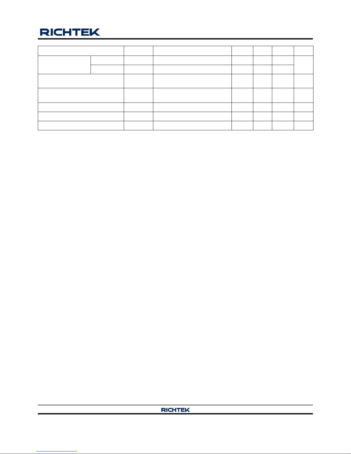
Outline Dimension
A
B
J
F
H
M
C
D
I
Y
X
EXPOSED THERMAL PAD
(Bottom of Package)
8-Lead SOP (Exposed Pad) Plastic Package
Dimensions In Millimeters Dimensions In Inches
Symbol
Min Max Min Max
A 4.801 5.004 0.189 0.197
B 3.810 4.000 0.150 0.157
C 1.346 1.753 0.053 0.069
D 0.330 0.510 0.013 0.020
F 1.194 1.346 0.047 0.053
H 0.170 0.254 0.007 0.010
I 0.000 0.152 0.000 0.006
J 5.791 6.200 0.228 0.244
M 0.406 1.270 0.016 0.050
X 2.000 2.300 0.079 0.091
Option 1
Y 2.000 2.300 0.079 0.091
X 2.100 2.500 0.083 0.098
Option 2
Y 3.000 3.500 0.118 0.138
 Loading...