

Page 1

RT7285CGJ6
Evaluation Board
UG7285CGJ6-00 January 2015 1 http://www.richtek.com
your power partner.
RT7285CGJ6 Evaluation Board
Purpose
The RT7285C is a synchronous step-down converter with Advanced Constant On-Time (ACOT™) mode control. It
can deliver up to 1.5A output current from a wide input voltage range of 4.3V to 18V. This document explains the
function and use of the RT7285C evaluation board (EVB) and provides information to enable operation and
modification of the evaluation board and circuit to suit individual requirements.
Table of Contents
PURPOSE ................................................................................................................................................................................ 1
INTRODUCTION ...................................................................................................................................................................... 2
KEY PERFORMANCE SUMMARY TABLE ................................................................................................................................... 2
BENCH TEST SETUP CONDITIONS............................................................................................................................................ 3
SCHEMATIC, BILL OF MATERIALS AND BOARD LAYOUT ........................................................................................................... 5
MORE INFORMATION........................................................................................................................................................... 10
IMPORTANT NOTICE FOR RICHTEK REFERENCE DESIGNS ...................................................................................................... 10
Page 2

RT7285CGJ6
Evaluation Board
UG7285CGJ6-00 January 2015 2 http://www.richtek.com
your power partner.
Introduction
General Product Information
The RT7285C is a synchronous step-down converter with Advanced Constant On-Time (ACOT™) mode control.
The ACOT™ provides a very fast transient response with few external components. The low impedance internal
MOSFET supports high efficiency operation with wide input voltage range from 4.3V to 18V. The proprietary circuit
of the RT7285C enables to support all ceramic capacitors. The output voltage can be adjusted between 0.6V and 8V.
The RT7285C also provides output under voltage protection and thermal shutdown protection. The low current
(<4μA) shutdown mode provides output disconnection, enabling easy power management in battery-powered
systems. The RT7285C is available in TSOT-23-6 package.
Product Feature
±1.5% High Accuracy Feedback Voltage
4.3V to 18V Input Voltage Range
1.5A Output Current
Integrated N-MOSFET Switches
ACOTTM mode control
Fixed Frequency Operation : 500kHz
Output Adjustable from 0.6V to 8V
Up to 95% Efficiency
Fast Transient Response
Stable with Low-ESR Ceramic Output Capacitors
Cycle-by-Cycle Over Current Protection
Input Under Voltage Lockout
Output Under Voltage Protection
Thermal Shutdown Protection
RoHS Compliant and Halogen Free
Key Performance Summary Table
Key Features
Evaluation Board Number: PCB007_V1
Default Input Voltage
12V
Max Output Current
1.5A
Default Output Voltage
1.2V
Default Marking & Package Type
RT7285CGJ6, TSOT-23-6
Operation Frequency
Steady 500kHz at all loads
Other Key Features
ACOTTM for Fast Transient Response
Protection
Output Under-Voltage Protection (hiccup mode):
Cycle-by-cycle Current Limit
Thermal Shutdown
Page 3

RT7285CGJ6
Evaluation Board
UG7285CGJ6-00 January 2015 3 http://www.richtek.com
your power partner.
Bench Test Setup Conditions
Headers Description and Placement
Please carefully inspect the EVB IC and external components, comparing them to the following Bill of Materials, to ensure that all components are
installed and undamaged. If any components are missing or damaged during transportation, please contact the distributor or send e-mail to
evb_service@richtek.com
Test Points
The EVB is provided with the test points and pin names listed in the table below.
Test point/
Pin name
Signal
Comment (expected waveforms or voltage levels on test points)
VIN
Input voltage
Input voltage range= 4.3V to 18V
VOUT
Output voltage
Default output voltage = 1.2V
Output voltage range= 0.6V to 8V
(see ‘’ Output Voltage Setting’’ section for changing output voltage level)
SW
Switching node test point
SW waveform
EN
Enable test point
Enable signal. Drive EN or install a shorting block on Jumper JP2 to
enable operation or disable operation.
JP2
Chip enable control
Install jumper or drive EN directly to enable or disable operation
BOOT
Boot strap supply test point
Floating supply voltage for the high-side N-MOSFET switch
GND
Ground
Ground
Power-up & Measurement Procedure
1. Apply a 12V nominal input power supply (4.3V < VIN < 18V) to the VIN and GND terminals.
2. The EN voltage is pulled to logic high by R5 (100kΩ to VIN) to enable operation. Drive EN high (>1.5V) to
enable operation or low (<0.4V) to disable operation.
3. Verify the output voltage (approximately 1.2V) between VOUT and GND.
4. Connect an external load up to 1.5A to the VOUT and GND terminals and verify the output voltage and current.
Page 4

RT7285CGJ6
Evaluation Board
UG7285CGJ6-00 January 2015 4 http://www.richtek.com
your power partner.
Output Voltage Setting
Set the output voltage with the resistive divider (R2, R3) between VOUT and GND with the midpoint connected to
FB. The output is set by the following formula:
The installed VOUT capacitors (C9, C10) are 22μF, 16V X5R ceramic types. Do not exceed their operating voltage
range and consider their voltage coefficient (capacitance vs. bias voltage) and ensure that the capacitance is
sufficient to maintain stability and provide sufficient transient response for your application. This can be verified by
checking the output transient response as described in the RT7285C IC datasheet.
Page 5

RT7285CGJ6
Evaluation Board
UG7285CGJ6-00 January 2015 5 http://www.richtek.com
your power partner.
Schematic, Bill of Materials & Board Layout
EVB Schematic Diagram
C3, C4: 10μF/50V/X5R, 1206, TDK C3216X5R1H106K
C9, C10: 22μF/16V/X5R, 1210, Murata GRM32ER61C226K
L1: 2μH TAIYO YUDEN NR8040T2R0N, DCR=9mΩ
Page 6

RT7285CGJ6
Evaluation Board
UG7285CGJ6-00 January 2015 6 http://www.richtek.com
your power partner.
Bill of Materials
Reference
Qty
Part number
Description
Package
Manufacture
U1
1
RT7285CGJ6
DC-DC Converter
TSOT-23-6 (FC)
RICHTEK
C3, C4
2
C3216X5R1H106K160AB
10μF/±10%/50V/X5R
Ceramic Capacitor
1206
TDK
C9, C10
2
GRM32ER61C226KE20#
22μF/±10%/16V/X5R
Ceramic Capacitor
1210
Murata
C6, C8, C12
3
C1608X7R1H104K080AA
0.1μF/±10%/50V/X7R
Ceramic Capacitor
0603
TDK
C1, C11, D2
0 Not Installed
0603
L1
1
NR8040T2R0N
2.0μH/7.4A/±30%,
DCR=9mΩ, Inductor
8mmx8mmx4mm
TAIYO YUDEN
R2
1 10kΩ/±1%, Resistor
0603
R3
1 10kΩ/±1%, Resistor
0603
R5
1 100kΩ/±1%, Resistor
0603
CP1
1
Short
JP2, J5
2 3-Pin Header
GP
4
EN, B( E), BOOT, SW
Golden Pin
TP
3
Vout, GND, VIN
Test Pin
J3, J6, J7, J8
4
VIN, VOUT, GND, GND
Test Pin
Page 7

RT7285CGJ6
Evaluation Board
UG7285CGJ6-00 January 2015 7 http://www.richtek.com
your power partner.
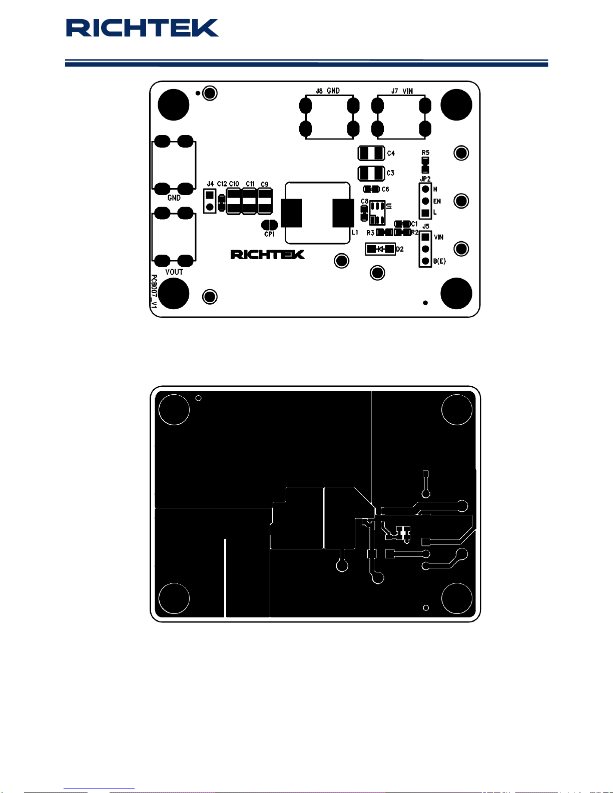
EVB Layout
Top View (1
st
layer)
Bottom View (4th Layer)
Page 8
RT7285CGJ6
Evaluation Board
UG7285CGJ6-00 January 2015 8 http://www.richtek.com
your power partner.
Component Placement Guide—Component Side (1
st
layer)
PCB Layout—Component Side (1
st
Layer)
Page 9

RT7285CGJ6
Evaluation Board
UG7285CGJ6-00 January 2015 9 http://www.richtek.com
your power partner.
PCB Layout—Bottom Side (4th layer)
Page 10

RT7285CGJ6
Evaluation Board
UG7285CGJ6-00 January 2015 10 http://www.richtek.com
your power partner.
More Information
For more information, please find the related datasheet or application notes from Richtek website
http://www.richtek.com.
Important Notice for Richtek Evaluation Board
THIS DOCUMENT IS FOR REFERENCE ONLY, NOTHING CONTAINED IN THIS DOCUMENT SHALL BE CONST RUED AS RICHTEK’S WARRANTY, EXPRESS
OR IMPLIED, UNDER CONTRACT, TORT OR STATUTORY, WITH RESPECT TO THE PRESENTATION HEREIN. IN NO EVENT SHALL RICHTEK BE LIABLE TO
BUYER OR USER FOR ANY AND ALL DAMAGES INCLUDING WITHOUT LIMITATION TO DIRECT, INDIRECT, SPECIAL, PUNITIVE OR CONSEQUENTIAL
DAMAGES.
 Loading...