

Page 1
®
PMIC for Industrial Application
RT5028
General Description
The RT5028 is a highly-integrated low-power highperformance analog SOC with PMIC in one single chip
designed for Industrial a pplications.
The RT5028 includes four synchronous step-down DC/
DC converters and eight LDOs for syste m power.
The RT5028 also embeds one EEPROM (MTP) for setting
sequence and timing etc.
Additionally, the RT5028 PMIC also includes one IRQ
report.
Applications
Industrial
Ordering Information
RT5028
Package Type
QW : WQFN-56L 7x7 (W-Type)
Lead Plating System
G : Green (Halogen Free and Pb Free)
Note :
Richtek products are :
RoHS compliant and compatible with the current require-
ments of IPC/JEDEC J-STD-020.
Suitable for use in SnPb or Pb-free soldering processes.
Features
Input Voltage Operating Range is 3.3V to 5.5V
Step-Down Regulator : V
Max Current 2.4A/2A/1.6A/2A
Programmable Frequency from 500kHz to 2MHz
2
I
C Programmable Output Level
2
I
C Programmable Operation Mode (Force PWM
or Auto PSM/PWM)
2
I
C Programmable Output Discharge Mode
(Discharge or Flatting)
Linear Regulators : V
Max Current 0.3A
2
I
C Programmable Output Level
Embedded 32Bytes MTP for Factory T uning
External MTP Pin for Write Protection
Sequence can be Controlled by I
Defined by MASK_GPIO pin.
OT/UVP/VIN LV/POWRON press Time Interrupt
(IRQ).
2
I
C Control Interface: Support Fast Mode up to
400kb/s
RoHS Compliant and Halogen Free
Range is 3.3V to 5.5V
IN
Range is 2.5V to 5.5V
IN
2
C or each EN pins
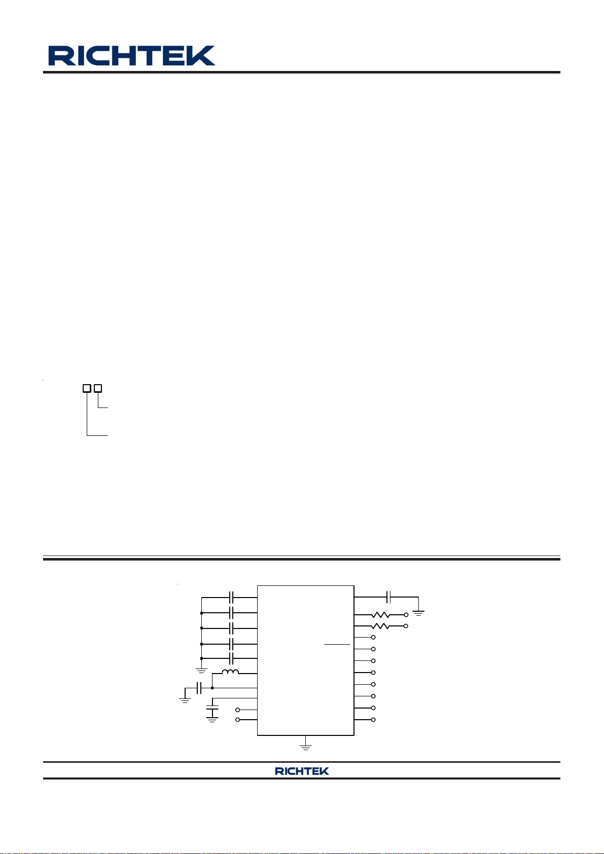
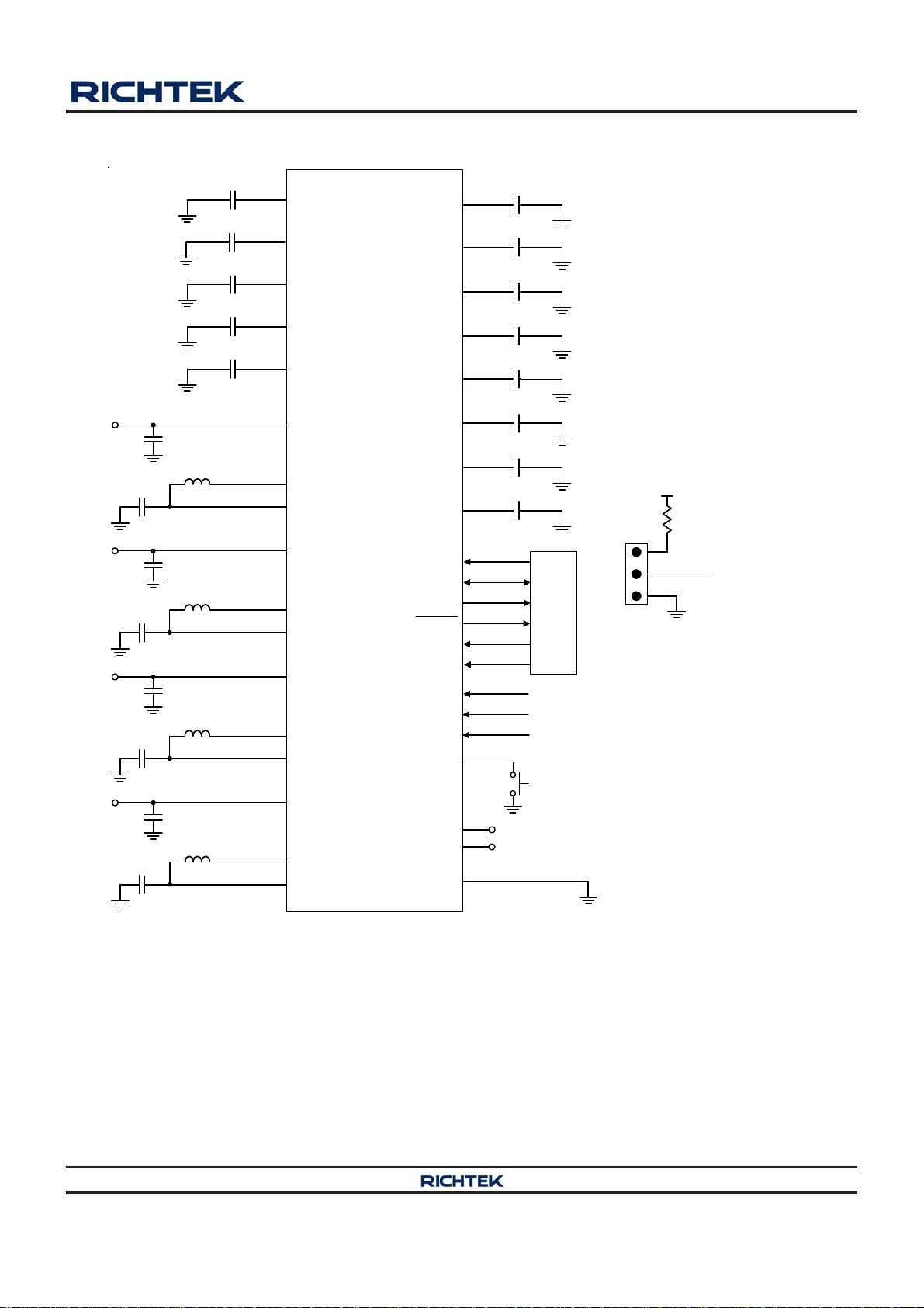
Simplified Application Circuit
VIN
VDDP
VINL123
VINL456
VINL78
LXBx
VOUTBxS
VINBx
ENBx
ENLx
Copyright 2015 Richtek Technology Corporation. All rights reserved. is a registered trademark of Richtek Technology Corporation.
©
DS5028-01 January 2015 www.richtek.com
RT5028
PWRHOLD
REBOOT
MASK_GPIO
AGND
VOUTLx
SCL
SDA
IRQ
RESET
PWRON
MTP
SADDR
1
Page 2
RT5028
Marking Information
RT5028GQW : Product Number
RT5028
GQW
YMDNN
YMDNN : Date Code
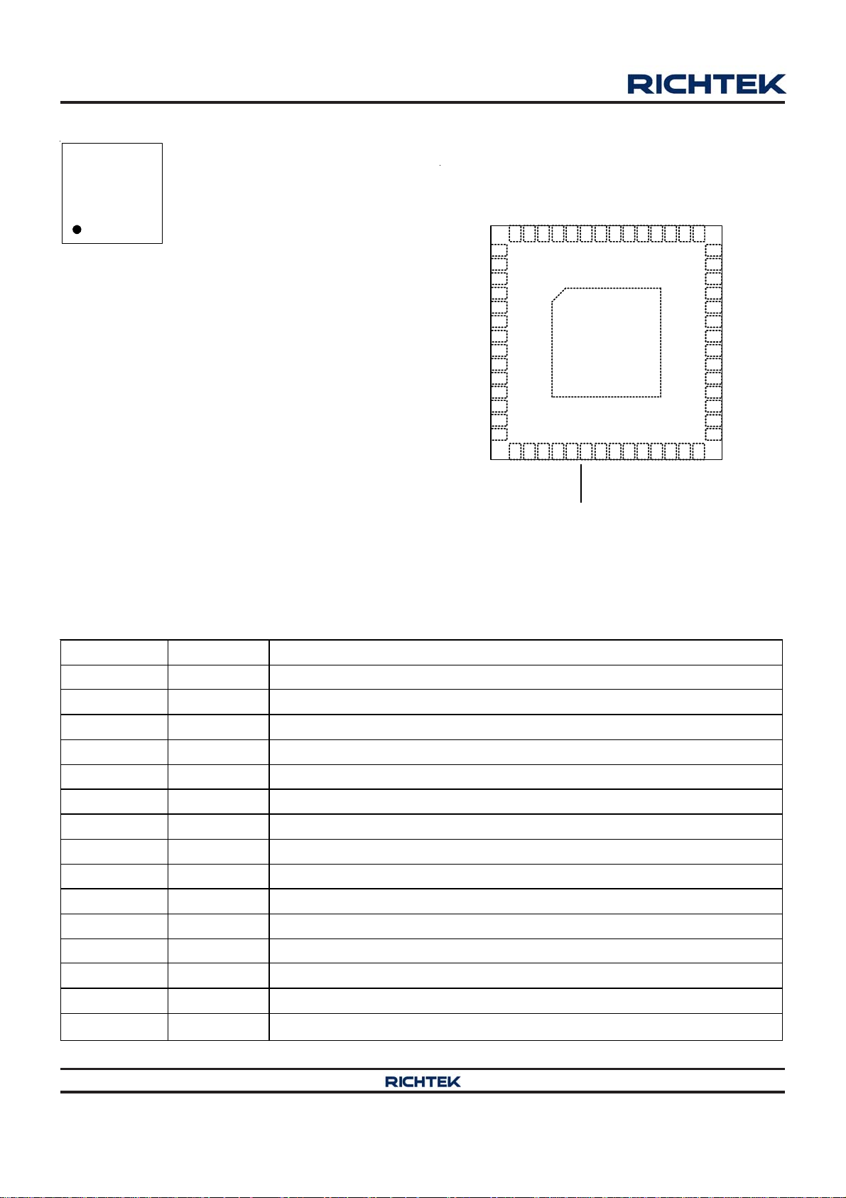
Pin Configurations
(TOP VIEW)
ENL3
ENL2
ENL1
VIN
VDDP
IRQ
VOUTB1S
AGND
AGND
RESET
VOUTL1
VINL123
VOUTL2
VOUTL3
VOUTL6
VOUTL5
VINL456
VOUTL4
VOUTL7
VINL78
VOUTL8
ENL4
ENL5
ENL6
AGND
1
2
3
4
5
6
7
8
9
10
11
12
13
14
SCL
SDA
ENL7
ENL8
ENB1
PWRON
LXB1
LXB1
57
MTP
REBOOT
VINB1
VINB1
454647484950515253545556
44
262524232221201918171615
27
PWRHOLD
MASK_GPIO
VINB2
43
28
SADDR
VINB2
42
41
40
39
38
37
36
35
34
33
32
31
30
29
ENB4
LXB2
LXB2
ENB2
VOUTB2S
VINB3
VINB3
LXB3
LXB3
AGND
VOUTB3S
VINB4
LXB4
ENB3
VOUTB4S
Functional Pin Description
Pin No. Pin Name Pin Function
1 VOUTL1 Output Voltage Regulation Node for LDO1.
2 VINL123 Input Power f or LDO1, LDO2 and LDO3.
3 VOUTL2 Output Voltage Regulation Node for LDO2.
4 VOUTL3 Output Voltage Regulation Node for LDO3.
5 VOUTL6 Output Voltage Regulation Node for LDO6.
6 VOUTL5 Output Voltage Regulation Node for LDO5.
7 VINL456 Input Power f or LDO4, LDO5 and LDO6.
8 VOUTL4 Output Voltage Regulation Node for LDO4.
9 VOUTL7 Output Voltage Regulation Node for LDO7.
10 VINL78 Input Power for LDO7 and LDO8.
11 VOUTL8 Output Voltage Regulation Node for LDO8.
12 ENL4 Enable Control Input for LDO4. Connect a 100k pull-low resistor.
WQFN-56L 7x7
13 ENL5 Enable Control Input for LDO5. Connect a 100k pull-low resistor.
14 ENL6 Enable Control Input for LDO6. Connect a 100k pull-low resistor.
15 SCL Clock Input for I2C. Open-drain output, connect a 10k pull-up resistor.
Copyright 2015 Richtek Technology Corporation. All rights reserved. is a registered trademark of Richtek Technology Corporation.
2
©
DS5028-01 January 2015www.richtek.com
Page 3
Pin No. Pin Name Pin Function
16 SDA
Data Input for I
2
C. Open-drain output, c onnec t a 10k pull-up resistor.
17 ENL7 Enabl e Control Input for LDO7. Connect a 100k pull-low resistor.
18 ENL8 Enabl e Control Input for LDO8. Connect a 100k pull-low resistor.
19 IRQ Open-Drain IRQ Output Node.
RT5028
20
21, 34, 56, 57
(Exposed Pad)
RESET
AGND
Reset Output.
Analog Ground. The exposed pad must be soldered to a large PCB and
connected to AGND for maximum power dissipation.
22 PWRON Manual Power On. Connect a 100k pull - up resistor.
23 REBOOT System Power Reboot. Connec t a 100k pull-low resistor.
24 MTP
25 MASK_GPIO
MTP Write Protection Pin. Connect a 100k pull-low resistor, logic low is
inhibit ed and logic high is permit to write.
Select I
2
C or use EN pin for Bucks and LDOs. Connect a 100k pull-low resistor.
As MASK_GPIO is high, ignor e all E N pins.
As MASK_GPIO is low, EN pins and I
2
higher than I
C.
2
C both can control. EN pins priority is
26 PWRHOL D Power Hold Input. Connec t a 100k p ull -low resistor.
27 SADDR I2C Slave Address. Connect a 100k pull-low resistor.
28 ENB4 Enable Control Input for Buck4. Connect a 100k pull -low resi stor.
29 VOUTB4S Output Voltage Regulation Node for Buck4.
30 ENB3 Enable Control Input for Buck3. Connect a 100k pull -low resist or.
31 LXB4 Internal Switc h Node to Output Inductor Connecti on for Buck4.
32 VINB4 Input Power for Buck 4.
33 VOUTB3S Output Voltage Regulation Node for Buck3.
35, 36 LXB3 Internal Switch Node t o Output Inductor Connection for Buc k 3.
37, 38 VINB3 I nput Power for Buck3.
39 VOUTB2S Output Voltage Regulation Node for Buck2.
40 ENB2 Enable Control Input for Buck2. Connect a 100k pull -low resi stor.
41, 42 LXB2 Internal Switch Node t o Output Inductor Connection for Buc k 2.
43, 44 VINB2 I nput Power for Buck2.
45, 46 VINB1 I nput Power for Buck1.
47, 48 LXB1 Internal Switch Node t o Output Inductor Connection for Buc k 1.
49 ENB1 Enable Control Input for Buck1. Connect a 100k pull -low resi stor.
50 VOUTB1S Output Voltage Regulation Node for Buck1
51 VDDP Internal Bi as Regulator Voltage. Exter nal load on this pin is not allowed.
52 VIN Input Power for Analog B ase.
53 ENL1 Enabl e Control Input for LDO1. Connect a 100k pull-low resistor.
54 ENL2 Enabl e Control Input for LDO2. Connect a 100k pull-low resistor.
55 ENL3 Enabl e Control Input for LDO3. Connect a 100k pull-low resistor.
Copyright 2015 Richtek Technology Corporation. All rights reserved. is a registered trademark of Richtek Technology Corporation.
DS5028-01 January 2015 www.richtek.com
©
3
Page 4
RT5028
Function Block Diagram
VOUTL1
VINL123
VOUTL2
VOUTL3
VOUTL4
VINL456
VOUTL5
VOUTL6
VOUTL7
VINL78
VOUTL8
SDA
SCL
IRQ
RESET
PWRHOLD
REBOOT
MTP
MASK_GPIO
SADDR
PWRON
ENB1 to ENB4
ENL1 to ENL8
AGND
LDO1
300mA
LDO2
300mA
LDO3
300mA
LDO4
300mA
LDO5
300mA
LDO6
300mA
LDO7
300mA
LDO8
300mA
State
Machine
Central
Controller
2
C
I
Programmable
Analog
Base
Buck1
2.4A
Buck2
2A
Buck3
1.6A
Buck4
2A
GND
GND
GND
GND
VIN
VDDP
VINB1
LXB1
VOUTB1S
VINB2
LXB2
VOUTB2S
VINB3
LXB3
VOUTB3S
VINB4
LXB4
VOUTB4S
Copyright 2015 Richtek Technology Corporation. All rights reserved. is a registered trademark of Richtek Technology Corporation.
©
DS5028-01 January 2015www.richtek.com
4
Page 5

Operation
RT5028
The RT5028 is a highly-integrated solution for industrial
system including 4-CH step-down DC/DC converters a nd
8-CH LDOs. The RT5028 a pplication mecha nism will be
introduced in later sections.
The power-on and power-off sequences ca n be controlled
by I2C or each EN pin and detected in MASK_GPIO pin.
When the MASK_GPIO pin is at Hi level, the PMIC follows
the power-on sequence to turn on channels. When the
MASK_GPIO pin is at Lo level, the channels of PMIC will
be controlled by the EN pin.
Synchronous Step-Down DC/DC Converter
Four current mode synchronous step-down DC/DC
converters operate with internal power MOSFETs, FB
resistors and compensation network. These cha nnels are
suitable for core power in industrial system. They ca n be
operated at 100% maximum duty cycle to extend battery
operating voltage range. When the input voltage is close
to the output voltage, the converter enters low dropout
mode with low output ripple. The operating frequency of
step-down converter is adjustable from 500kHz to 2MHz
and is controlled by I2C. Besides, the I2C interface also
can be used to select different operation mode s, On/Off
Sequence, programmable the output voltage, RAMP
control and discharge function. To enable AUTO Mode, it
is used to improve the efficiency at light load. If the AUTO
Mode is disabled, the converter operates in force PWM
mode with fixed switching frequency .
Over-Temperature Protection
An Over-T emperature Protection (OTP) is contained in the
device. The protection is triggered to force the device
shutdown for protecting itself when the junction
temperature exceeds 165°C typically. Once the junction
temperature drops below the hysteresis 10°C typically,
the device must be re-send PWRON to start system.
Output Under-Voltage Protection
The output under-voltage protection is implemented in order
to prevent operation at low output voltage conditions.
When the step-down DC/DC converters output voltage is
lower than 1/2 x (V
turns off immediately.
), the UVP event triggers and PMIC
OUT
Linear Regulator
Eight generic low voltage LDOs for multiple purpose power .
The LDOs are stable over the entire operating load ra nge
with the use of external ceramic capacitors. The LDOs
also have I2C programm able power on/off sequence a nd
discharge function. The output voltage is adjustable by
the I2C interface in the ra nge of 1.6V to 3.6V.
Copyright 2015 Richtek Technology Corporation. All rights reserved. is a registered trademark of Richtek Technology Corporation.
DS5028-01 January 2015 www.richtek.com
©
5
Page 6
RT5028
Absolute Maximum Ratings (Note 1)
Analog Ba se Input Voltage, VIN ---------------------------------------------------------------------------------------- −0.3V to 6V
PMIC Input V oltage, VINL123/456/78, VINB1/2/3/4 ---------------------------------------------------------------- −0.3V to 6V
PMIC Output V oltage, VOUTLx, VOUTBxS, LXBx----------------------------------------------------------------- −0.3V to 6V
PMIC related Other Pins-------------------------------------------------------------------------------------------------- −0.3V to 6V
Power Dissipation, P
WQFN-56L 7x7 ------------------------------------------------------------------------------------------------------------- 3.7W
Package Thermal Re sistance (Note 2)
WQF N-56L 7x7, θJA-------------------------------------------------------------------------------------------------------- 27°C/W
WQFN-56L 7x7, θJC------------------------------------------------------------------------------------------------------- 7°C/W
Junction T emperature------------------------------------------------------------------------------------------------------ 150°C
Lead T e mperature (Soldering, 10 sec.)-------------------------------------------------------------------------------- 260°C
Storage T emperature Range --------------------------------------------------------------------------------------------- −65°C to 150°C
ESD Susceptibility (Note 3)
HBM (Human Body Model)----------------------------------------------------------------------------------------------- 2kV
MM (Machine Model) ------------------------------------------------------------------------------------------------------ 200V
@ T
D
= 25°C
A
Recommended Operating Conditions (Note 4)
Junction T emperature Range--------------------------------------------------------------------------------------------- − 40°C to 125°C
Ambient T emperature Range--------------------------------------------------------------------------------------------- − 40°C to 85°C
Electrical Characteristics
(VIN = 3.3V to 5.5V, TA = −40°C to 85°C, unless otherwise specified)
Parameter Symbol Test Conditions Min Typ Max Unit
As f
> 1MHz, 3.3V VIN 5.5 V.
Operation Voltage of VIN
PMIC
Quiescent Curr ent IIN
Warning for Die
Temperature
Over-Temperature
Protection
OTP and Warning
Hysteresis
OTW
OTP -- 165 -- C
-- 10 -- C
SW
1MHz, VIN 4V.
If f
SW
VIN = 5V, LDOs, Bucks are ON with No Load. 300 450 600 A
= 5V, LDOs, Bucks are OFF.
V
IN
SCL = SDA = 0V
Temperature 1 -- 100 -Temperature 2 -- 125 --
3.3 -- 5.5 V
5 20 40 A
C
Input Pull-low 100k Resistor R
VIN = 5V, Temperature = 40C to 125C 70 115 160 k
Low
Copyright 2015 Richtek Technology Corporation. All rights reserved. is a registered trademark of Richtek Technology Corporation.
6
©
DS5028-01 January 2015www.richtek.com
Page 7
RT5028
t
Parameter Symbol Test Conditions Min Typ Max Unit
Buck1 to Buck4
Input Voltage V
Output Voltage V
Consumption
Current
INB
OUTB
I
VINB
Effi ciency Peak Eff
Output Voltage
Accuracy
Output Voltage
Ripple
V
OUTAcc
V
Rip
Output Voltage
Temperature
Coefficien
Switching
Frequency
Switching
Frequency Accuracy
-- ±100 -- ppm/C
f
SW
3.3 -- 5.5 V
Buck1 I
2
C Programmable per step 25mV
Buck2 I2C Programmable per step 25mV
Buck3 I2C Programmable per step 50mV
Buck4 I2C Programmable per step 50mV
AUTO Mode I
V
= 1.2V, V
OUT
3.6V
3.1V < V
1mA < I
I
OUT
I
OUT
I
2
C Pr ogr amma ble 0. 43 - - 2 M H z
1MHz f
IN
OUT
= 1m A , C
= 1A , C
SW
< 5.5V,
= 0mA, Each Buck 10 20 40 A
OUT
I
= CCM -- 88 --
LOAD
=
IN
I
= 1mA -- 80 --
LOAD
As VOUTB1S to VOUTB4 S 1V. 3 -- 3
< I
MAX
As VOUTB1S to VOUTB4S < 1V. 30 -- 30
= 10F, 2MHz -- 25 --
OUT
= 10F, 2MHz -- 8 --
OUT
10 -- 10
0.7 -- 1.8
0.7 -- 1.8
V
0.7 -- 3.6
0.7 -- 3.6
%
%mV
mV
%
fSW 1MHz 20 -- 20
S ugg est Induc t or L
Buck
Peak Current Limit OCP
Under-Voltage
Protection
Maximum Output
Current
Out put Transient
Response
High-Side
On-Resistance
Low-Side
On-Resistance
UVP VOUTB1S to VOUTB4S < 0.66 x (V
I
MAX
V
peak
R
pon
R
non
-- 2.2 -- H
Buck1 3.1 4.4 5.8
Buck2 2.8 4 5.2
A
Buck3 2.6 3.7 4.8
Buck4 2.8 4.1 5.3
Target) 56 66 76 %
OUT
Buck1 2.4 -- -Buck2 2 -- --
A
Buck3 1.6 -- -Buck4 2.0 -- --
0.8A to 1.6A at 20s, V
Buck1 and Buck2
OUT
= 1.2V
4 -- 4 %
VIN = 3.7V 50 150 250 m
VIN = 3.7V 40 110 160 m
Copyright 2015 Richtek Technology Corporation. All rights reserved. is a registered trademark of Richtek Technology Corporation.
DS5028-01 January 2015 www.richtek.com
©
7
Page 8
RT5028
Parameter Symbol Test Conditions Min Typ Max Unit
LDO1 to LDO8
Input Voltage for
VINL123/456/78
Output Voltage LDO123/78 V
Output Voltage LDO456 V
Output Current I
2.5 -- 5.5 V
V
INL
3.1V VIN 5.5V, 50A I
OUTL
3.1V V
OUTL
300 -- -- mA
OUT
5. 5V, 50A I
IN
OUT
OUT
I
I
3%
MAX
3%
MAX
1.6 to
3.6
3 to
3.6
3% V
3% V
Output Short Current Isht 330 450 600 mA
> 3.1V
V
V
Voltage Difference
Output Voltage Temperature
Coefficient
IN
V
OUT
-- ±100 -- ppm/C
Supply Current ISS I
Shutdown Current I
0 1 2 A
OFF
IN
VIN > 2.5V 0. 05 0. 11 0.5
= 0mA 10 35 60 A
OUT
V
IN
= V
SET
, I
OUT
= I
OUTMAX
0.05 0.1 0.3
V
Line Regulation Input 3V to 5V, load = 100mA 0 1 5 mV
Load Regulation V
T ra n sien t R espo n s e V
OUT
Ri pp le R eje cti on f = 1 0 kHz, I
Ri si ng Tim e V
Falling Time V
= 5V, Load 100mA to 300mA 0 0.1 1 %
IN
50A I
0.7 x V
OUT
0.3 x V
OUT
OUTMAX
/ 2 (⊿t = 1s) -- 50 -- mV
OUT
= I
Target
Target
OUTMAX
/ 2 -- 60 -- dB
, I
= 0mA 150 220 300 s
OUT
, I
= 0mA 300 600 1000 s
OUT
I2C Interface Elect rical Charac teristics
Voltage Output Low VOL -- -- 0.4 V
Input Voltage
High-Level V
1.5 -- --
IH
V
Low-Level VIL -- -- 0.4
SCL Clock SCL -- -- 400 kHz
Note 1. Stresses beyond those listed “Absolute Maximum Ratings” may cause permanent damage to the device. These are
stress ratings only, and functional operation of the device at these or any other conditions beyond those indicated in
the operational sections of the specifications is not implied. Exposure to absolute maximum rating conditions may
affect device reliability.
Note 2. θ
Note 3. Devices are ESD sensitive. Handling precaution is recommended.
Note 4. The device is not guaranteed to function outside its operating conditions.
is measured at T
JA
measured at the exposed pad of the package.
= 25°C on a high effective thermal conductivity four-layer test board per JEDEC 51-7. θJC is
A
Copyright 2015 Richtek Technology Corporation. All rights reserved. is a registered trademark of Richtek Technology Corporation.
8
©
DS5028-01 January 2015www.richtek.com
Page 9
Typical Application Circuit
RT5028
22µF
22µF
22µF
22µF
10µF
10µF
10µF
10µF
2.2µH
2.2µH
2.2µH
2.2µH
1µF
1µF
1µF
1µF
1µF
52
10
45, 46
47, 48
50
43, 44
41, 42
39
37, 38
35, 36
33
32
31
29
VIN
51
VDDP
2
VINL123
7
VINL456
VINL78
VINB1
LXB1
VOUTB1S
VINB2
LXB2
VOUTB2S
VINB3
LXB3
VOUTB3S
VINB4
LXB4
VOUTB4S
RT5028
PWRHOLD
MASK_GPIO
ENL1 to ENL8
ENB1 to ENB4
VOUTL1
VOUTL2
VOUTL3
VOUTL4
VOUTL5
VOUTL6
VOUTL7
VOUTL8
SCL
SDA
IRQ
RESET
REBOOT
MTP
SADDR
PWRON
AGND
1µF
1
1µF
3
1µF
4
1µF
8
1µF
6
1µF
5
1µF
9
1µF
11
15
16
19
20
26
23
24
25
27
22
21, 34, 56,
57 (Exposed Pad)
AP
VIN
SADDR
MASK_GPIOMTP
AGND
As SADDR connect to AGND
slave address
=0111111
As SADDR connect to VIN
slave address
=0110111
As MASK_GPIO connect to AGND
EN pins can control.
As MASK_GPIO connect to VIN
Ignore all EN pins.
As MTP connect to AGND
Inhibit to write MTP.
As MTP connect to VIN
Permit to write MTP.
Copyright 2015 Richtek Technology Corporation. All rights reserved. is a registered trademark of Richtek Technology Corporation.
©
DS5028-01 January 2015 www.richtek.com
9
Page 10
RT5028
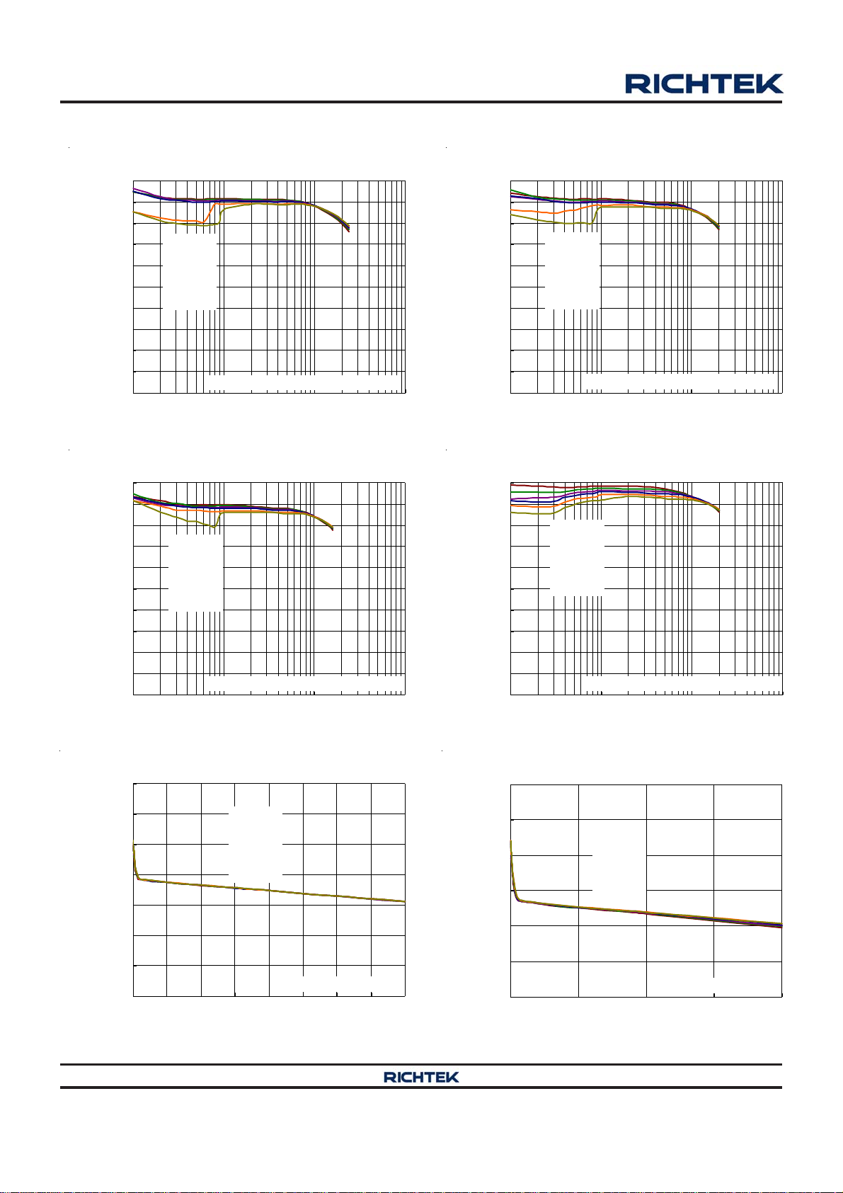
Typical Operating Characteristics
CH1 Buck Efficiency vs. Output Current
100
90
80
70
60
50
40
Effici ency (%)
30
20
10
0
VIN = 3.3V
VIN = 3.6V
VIN = 3.9V
VIN = 4.2V
VIN = 5V
VIN = 5.5V
V
= 1.35V, L = 2.2μH, C
OUT
10 100 1000 10000
OUT
Output Current (mA)
CH3 Buck Efficiency vs. Output Current
100
90
80
70
60
50
40
Effici ency (%)
30
20
10
0
VIN = 3.3V
VIN = 3.6V
VIN = 3.9V
VIN = 4.2V
VIN = 5V
VIN = 5.5V
V
= 1.2V, L = 2.2μH, C
OUT
10 100 1000 10000
OUT
Output Current (mA)
= 10μF
= 10μF
CH2 Buck Efficiency vs. Output Current
100
90
80
70
60
50
40
Efficiency (%)
30
20
10
0
VIN = 3.3V
VIN = 3.6V
VIN = 3.9V
VIN = 4.2V
VIN = 5V
VIN = 5.5V
V
= 1.5V, L = 2.2μH, C
OUT
10 100 1000 10000
OUT
Output Current (mA)
CH4 Buck Efficiency vs. Output Current
100
90
80
70
60
50
40
Eff iciency (%)
30
20
10
0
10 100 1000 10000
VIN = 3.6V
VIN = 3.9V
VIN = 4.2V
VIN = 4.5V
VIN = 5V
VIN = 5.5V
V
OUT
Output Current (mA)
= 3.3V, L = 2.2μH, C
OUT
= 10μF
= 10μF
CH1 Buck Output Voltage vs. Output Current
1.39
1.38
1.37
1.36
1.35
1.34
Output Voltage (V)
1.33
1.32
0 300 600 900 1200 1500 1800 2100 2400
Copyright 2015 Richtek Technology Corporation. All rights reserved. is a registered trademark of Richtek Technology Corporation.
©
VIN = 3.3V
VIN = 3.6V
VIN = 3.9V
VIN = 4.2V
VIN = 5V
VIN = 5.5V
L = 2.2μH, C
Output Current (mA)
OUT
= 10μF
CH2 Buck Output Voltage vs. Outpu t Current
1.53
1.52
1.51
1.50
1.49
Output Voltage (V)
1.48
1.47
0 500 1000 1500 2000
VIN = 3.3V
VIN = 3.6V
VIN = 3.9V
VIN = 4.2V
VIN = 5V
VIN = 5.5V
L = 2.2μH, C
Output Current (A)
OUT
DS5028-01 January 2015www.richtek.com
10
= 10μF
Page 11
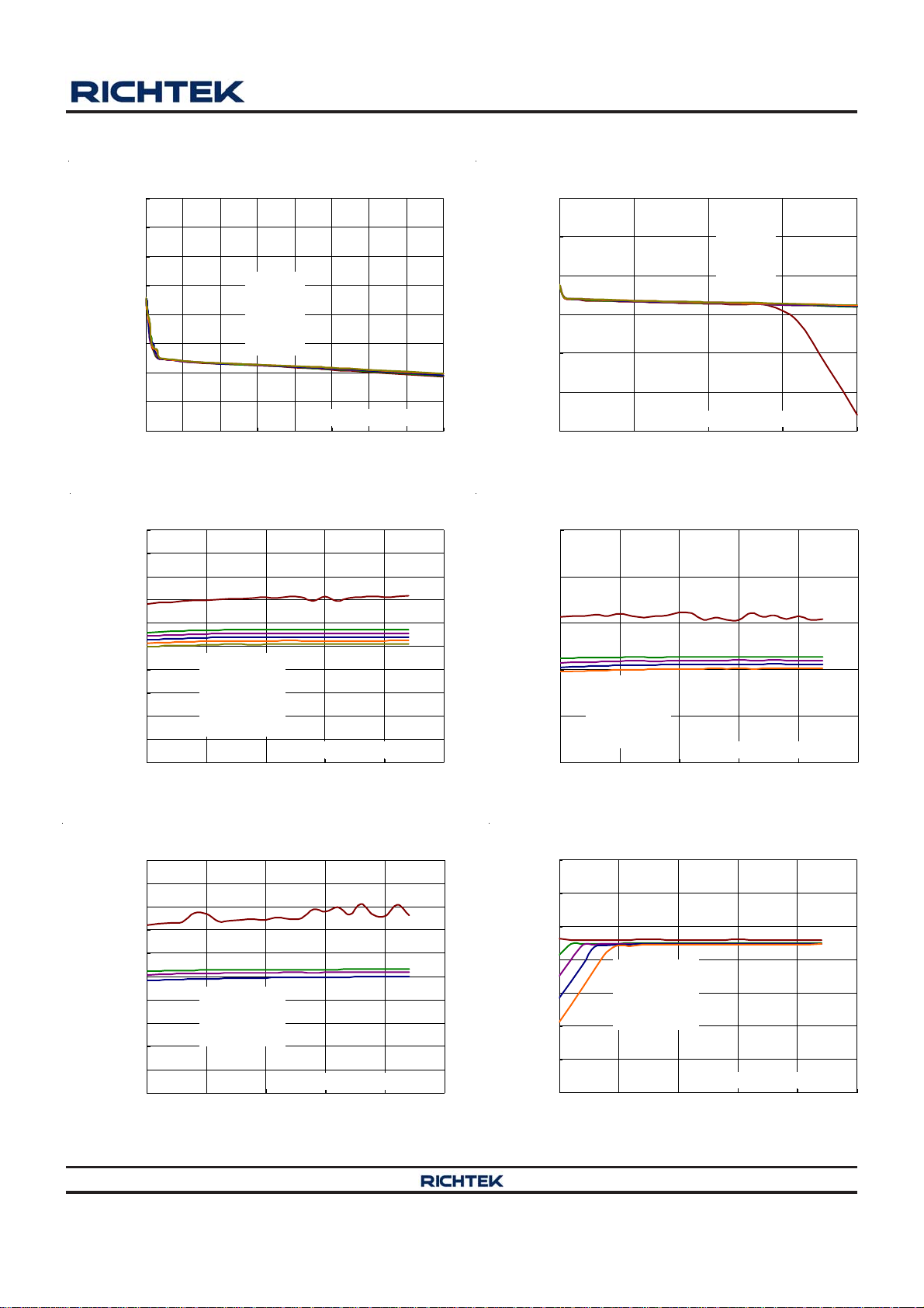
RT5028
CH3 Buck Output Voltage vs. Output Current
1.25
1.24
1.23
1.22
1.21
1.20
Output Voltage (V)
1.19
1.18
1.17
0 200 400 600 800 1000 1200 1400 1600
VIN = 3.3V
VIN = 3.6V
VIN = 3.9V
VIN = 4.2V
VIN = 5V
VIN = 5.5V
L = 2.2μH, C
OUT
= 10μF
Output Current (mA)
CH1 Buck Output Voltage vs. Input Voltage
1.40
1.39
1.38
1.37
1.36
1.35
1.34
1.33
Output Voltage (V)
1.32
1.31
1.30
3.3 3.8 4.3 4.8 5.3 5.8
I
= 0mA
OUT
I
= 500mA
OUT
I
= 1000mA
OUT
I
= 1500mA
OUT
I
= 2000mA
OUT
I
= 2400mA
OUT
Input Voltage (V)
L = 2.2μH, C
OUT
= 10μF
CH4 Buck Output Voltage vs. Output Current
3.38
VIN = 3.6V
3.33
VIN = 3.9V
VIN = 4.2V
VIN = 4.5V
3.28
3.23
3.18
VIN = 5V
VIN = 5.5V
Output Voltage (V)
3.13
3.08
L = 2.2μH, C
0 500 1000 1500 2000
OUT
= 10μF
Output Current (mA)
CH2 Buck Output Voltage vs. Input Voltage
1.55
1.53
1.51
Output V oltage (V)
1.49
1.47
1.45
I
= 0mA
OUT
I
= 500mA
OUT
I
= 1000mA
OUT
I
= 1500mA
OUT
I
= 2000mA
OUT
3.3 3.8 4.3 4.8 5.3 5.8
L = 2.2μH, C
OUT
= 10μF
Inpu t Voltage (V)
CH3 Buck Output Voltage vs. Input Voltage
1.24
1.23
1.22
1.21
1.20
1.19
1.18
1.17
Output Volt age (V)
1.16
1.15
1.14
3.3 3.8 4.3 4.8 5.3 5.8
Copyright 2015 Richtek Technology Corporation. All rights reserved. is a registered trademark of Richtek Technology Corporation.
©
I
= 0mA
OUT
I
= 500mA
OUT
I
= 1000mA
OUT
I
= 1600mA
OUT
Input Vol tage (V)
L = 2.2μH, C
OUT
= 10μF
CH4 Buck Output Voltage vs. Input Voltage
3.80
3.60
3.40
3.20
3.00
2.80
Output Voltage (V)
2.60
2.40
3.3 3.8 4.3 4.8 5.3 5.8
I
= 0mA
OUT
I
= 500mA
OUT
I
= 1000mA
OUT
I
= 1500mA
OUT
I
= 2000mA
OUT
Inp ut Voltage (V)
L = 2.2μH, C
OUT
= 10μF
DS5028-01 January 2015 www.richtek.com
11
Page 12
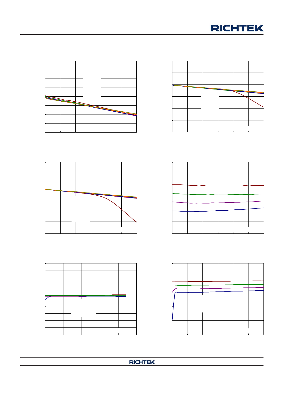
RT5028
Output Volt age (V)
Output Voltage (V)
LDO2 Output Voltage vs. Output Current
1.790
1.785
1.780
1.775
1.770
1.765
1.760
1.755
1.750
0 50 100 150 200 250 300
VIN = 2.5V
VIN = 3V
VIN = 3.6V
VIN = 4.2V
VIN = 5V
VIN = 5.5V
Output Current (mA)
LDO7 Output Voltage vs. Output Current
2.52
2.50
2.48
2.46
2.44
2.42
2.40
0 50 100 150 200 250 300
VIN = 2.5V
VIN = 3V
VIN = 3.6V
VIN = 4.2V
VIN = 5V
VIN = 5.5V
Output Current (mA)
LDO5 Output Voltage vs. Output Current
3.32
3.30
3.28
3.26
VIN = 3.3V
VIN = 3.6V
VIN = 3.9V
3.24
Output Voltage (V)
3.22
C
= 1μF
OUT
3.20
0 50 100 150 200 250 300
VIN = 4.2V
VIN = 5V
VIN = 5.5V
C
= 1μF
OUT
Output Current (mA)
LDO2 Output Voltage vs. Input Voltage
1.78
1.78
I
= 0mA
OUT
1.77
1.77
1.76
Output Voltage (V)
1.76
C
= 1μF
OUT
1.75
2.5 3 3.5 4 4.5 5 5.5
I
= 100mA
OUT
I
= 200mA
OUT
I
= 300mA
OUT
Input Voltage (V)
C
= 1μF
OUT
LDO5 Out put Volt age vs. Input Volt age
3.50
3.45
3.40
3.35
3.30
3.25
3.20
3.15
Output Voltage (V)
3.10
3.05
3.00
3.3 3.8 4.3 4.8 5.3 5.8
Copyright 2015 Richtek Technology Corporation. All rights reserved. is a registered trademark of Richtek Technology Corporation.
©
I
= 0mA
OUT
I
= 100mA
OUT
I
= 200mA
OUT
I
= 300mA
OUT
Inp ut Voltage (V)
Output Voltage (V)
C
= 1μF
OUT
LDO7 Output Voltage vs. Input Voltage
2.50
2.48
2.46
2.44
2.42
2.40
2.5 3 3.5 4 4.5 5 5.5
I
= 0mA
OUT
I
= 100mA
OUT
I
= 200mA
OUT
I
= 300mA
OUT
Input Voltage (V)
C
OUT
DS5028-01 January 2015www.richtek.com
12
= 1μF
Page 13

Application Information
RT5028
The RT5028 is a highly-integrated solution for industrial
system including PMIC and memory system. The R T5028
application me cha nism a nd I2C compatible interface are
introduced in later sections. The system's slave address
Detail time sequence control is described in Power ON/
OFF diagram. The I2C interface can program individual
regulator output voltage as well as on/off control and
voltage setting.
is 01 10111 (As SADDR = high) or 0111111(As SADDR =
low).
PMIC - Power management system provides 8 low dropout
linear regulator and 4 high efficiency synchronous ste pdown DC/DC converters. Power-On and Power-Off
sequences are control by PWRON and RESET in put pins.
I2C Interface Timing Diagram
The RT5028 acts a s an I2C -bus slave. The I2C-bus master
configures the settings for all function blocks by sending
command bytes to the RT5028 vi a the 2-wire I2C-bus. The
I2C timing diagrams are list in the following.
Read Function
Reading One Indexed Byte of Data from RT (With 1-Byte)
Acknowledge from RT Acknowledge from RT Acknowledge from Master
S Slave Address 0 A Register Address A Data Byte A P
R/W
Repeated Start R/W
Sr Slave Address 1 A
Acknowledge from RT
1Byte
Reading n Indexed W ords of Data from RT (With N-Byte)
Acknowledge from RT Acknowledge from RT
Acknowledge from RT
S Slave Address 0 A Register Address A
Repeated Start
Acknowledge from Master Acknowledge from Master
Data Byte A Data Byte A
1st Byte 2nd Byte (n-1)th Byte nth Byte
Sr Slave Address 1 A
R/WR/W
Acknowledge from Master Acknowledge from Master
……
Data Byte A Data Byte A P
Write Function
Writing One Byte of Data to RT (With 1-Byte)
Acknowledge from RT Acknowledge from RT Acknowledge from RT
S Slave Address 0 A Register Address A Data Byte A P
R/W
1Byte
Writing n Bytes of Data to RT (With N-Byte)
Acknowledge from RT Acknowledge from RT
S Slave Address 0 A Register Address A
R/W
Acknowledge from RT
Data Byte
1st Byte
Acknowledge from RT Acknowledge from RT
Acknowledge from RT
A
Data Byte
2nd Byte
A
…
Data Byte A Data Byte A P
(n-1)th Byte nth By te
Copyright 2015 Richtek Technology Corporation. All rights reserved. is a registered trademark of Richtek Technology Corporation.
©
DS5028-01 January 2015 www.richtek.com
13
Page 14

RT5028
PMIC
Power Channels Control Methodology
When VIN power Good or PW RON event occurs, the PMIC
will follow the power on sequence to turn on channels.
During normal operation, users can use the REBOOT pin
Power Off
Edge
trigger
No
PWRON
Check
Yes
1
(Internal I
2
C)
Mask_GPIO
to restart PMIC again. Another PWROFF event, OTP or
UVP occurs, PMIC will execute the power off. In the
RT5028 PMIC, the UVP event will be set out when the
Buck1 to Buck4s' output voltage is lower than 1/2 x (V
Edge
trigger
VIN Power
Good
No
Yes
0
(External Enable Control)
OUT
).
Yes
REBOOT
Check
Power On
Sequence
Normal Operation
No
OTP Check UVP Check
External EN
Check
Yes
NoNo
YesYes Yes
Power Off
No
PWROFF
Check
Yes
REBOOT
Check
No
Copyright 2015 Richtek Technology Corporation. All rights reserved. is a registered trademark of Richtek Technology Corporation.
©
DS5028-01 January 2015www.richtek.com
14
Page 15

PMIC - POWER ON/OFF Setting
The circuit setting for communication between RT5028
and A P is showed as below.
SCL
SDA
IRQ
RESET
PWRHOLD
State
Machine
REBOOT
MTP
MASK_GPIO
SADDR
PWRON
ENL1 to ENL8
ENB1 to ENB4
VIN
SADDR
MASK_GPIOMTP
AGND
AP
As SADDR connect ot AGND
slave address
=0111111
As SADDR connect ot VIN
slave address
=0110111
As MASK_GPIO connect ot
AGND
EN pins can control.
As MASK_GPIO connect ot VIN
Ignore all EN pins.
RT5028
Power Hold Function
When the “PWRHOLD” signal does not come during
THOLD time, the RT5028 will do shutdown sequence.
START_TIME
PWRON
BUCK1
……
BUCK4
LDO1
……
LDO8
As MTP connect ot AGND
Inhibit to write MTP.
As MTP connect ot VIN
Permit to write MTP.
If users want to disable power hold function, set
“DisTHOLD” bit in I2C register 10 bit[0] to disable this
function. In the timing diagra m below, the “THOLD” and
“RESET_DLY” can be set by MTP program.
RESET_DLY
Turn off sequence :
First-on-last-Off
RESET
PWRHOLD
Copyright 2015 Richtek Technology Corporation. All rights reserved. is a registered trademark of Richtek Technology Corporation.
©
Always Low
THOLD
DS5028-01 January 2015 www.richtek.com
15
Page 16

RT5028
When AP sends the “PWRHOLD” signal during THOLD ti me, the RT5028 will keep power-on.
START_TIME
PWRON
BUCK1
……
BUCK4
LDO1
……
LDO8
RESET_DLY
RESET
PWRHOLD
Timing Based ON/OFF Sequence
START_TIME
PWRON
BUCK1
TSS
BUCK2
……
BUCK4
LDO1
……
LDO8
Normal power on
TSS
...
SHDN_PRESS
RESET_DLY
THOLD
Low to High signal from AP.
Normal power off
TSS
TSS
RESET
Copyright 2015 Richtek Technology Corporation. All rights reserved. is a registered trademark of Richtek Technology Corporation.
©
DS5028-01 January 2015www.richtek.com
16
Page 17

Level Based ON/OFF Sequence
RT5028
PWRON
BUCK1
BUCK2
……
BUCK4
LDO1
……
LDO8
RESET
START_TIME
Normal power on
>80 %
>80 %
>80 %
>80 %
RESET_DLY
SHDN_PRESS
Normal power off
8ms
8ms
Abnormal OFF
PWRON
BUCK1
BUCK2
BUCK4
IRQ
……
LDO1
……
LDO8
START_TIME
TSS
Normal power on
TSS
RESET_DLY
IRQ Even Occur
SHDN_DLYTIME
Abnormal power off
RESET
Copyright 2015 Richtek Technology Corporation. All rights reserved. is a registered trademark of Richtek Technology Corporation.
©
DS5028-01 January 2015 www.richtek.com
17
Page 18

RT5028
PMU On/Off Sequence Setting
In the RT5028, users can set the power on/of f sequence and output voltage by I2C register 0x01 to 0x04 for Buck output
voltage, 0x07 to 0x0E for LDO output voltage and 0x2C to 0X32 f or startup sequence setting.
In the table below, users must set one by one (continue s number) a nd missing code is not allowed.
If users miss sequence code, the RT5028 will wait for next channel and the IC will be hold in waiting status.
Output Voltage Setting Startup Sequence Setting
Buck1
Buck1Output[5:0] Buck1_Seq[3:0]
[000000] [0001]
Buck2
Buck2Output[5:0] Buck2_Seq[3:0]
[101100] [0010]
Buck3
Buck3Output[5:0] Buck3_Seq[3:0]
[000000] [0011]
Buck4
Buck4Output[5:0] Buck4_Seq[3:0]
[101100] [0100]
LDO1
LDO1OUT[6:0] LDO1_Seq[3:0]
[0000000] [0101]
LDO2
LDO2OUT[6:0] LDO2_Seq[3:0]
[0101000] [0110]
LDO3
LDO3OUT[6:0] LDO3_Seq[3:0]
[0000000] [0111]
LDO4
LDO4OUT[6:0] LDO4_Seq[3:0]
[0101000] [1000]
LDO5
LDO5OUT[6:0] LDO5_Seq[3:0]
[0000000] [1001]
LDO6
LDO6OUT[6:0] LDO6_Seq[3:0]
[0101000] [1010]
LDO7
LDO7OUT[6:0] LDO7_Seq[3:0]
[0000000] [1011]
LDO8
LDO8OUT[6:0] LDO8_Seq[3:0]
[0101000] [1100]
Startup Enable Method
(Soft-Start Control)
[10]
Note :
* Output Voltage Setting: fill relative binary code to set the output voltage.
* Startup Sequence Setting :
“0000” denotes no operation (disable).
“0001” denotes first-startup.
“1100 to 1111” denotes last-startup.
If same number, it means startup at the same time.
*Startup Enable Method :
[01] to [11] : each startup enable interval time (1ms, 4ms, 8ms).
[00] : start end voltage (the output voltage's 80%)
Copyright 2015 Richtek Technology Corporation. All rights reserved. is a registered trademark of Richtek Technology Corporation.
18
©
DS5028-01 January 2015www.richtek.com
Page 19

RT5028
Synchronous Step-Down DC/DC Converter
Four current mode synchronous step-down DC/DC
converters operate with internal power MOSFETs and
compensation network. These channels supply the power
core chip of portable system. They can be operated at
100% maximum duty cycle to extend battery operating
voltage range. When the input voltage is close to the output
voltage, the converter enters low dropout mode with low
output ripple. The operating frequency range of ste p-down
converter is 0.5MHz to 2MHz.
Four step-down converters have RAMP control function
a s the following diagra m.
DC/DC 1/2/3/4
Output Voltage4
DC/DC 1/2/3/4
Output Voltage2
DC/DC 1/2/3/4
Output Voltage1
DC/DC 1/2/3/4
Output Voltage3
REBOOT Function
As the REBOOT pin is set from low to high, the REBOOT
function will be active. The REBOOT's FSM is shown as
below. It concludes 100ms de-bouncing ti me and delay1/
delay2 power off delay time.
Table 1. REBOOT Input Control Setting
Description Default
delayed2 10
delayed1
Action
00 : 100ms 10 : 1s
01 : 500ms 11 : 2s
delayed1 power-off then
delayed2 power-on PMIC
10
From “LOW“ to “HIGH” rising
input into REBOOT pin with
100ms debouncing time
Wait for delayed1 time
Power off the PMIC
Wait for delayed2 time
Power on the PMIC
IRQ Table
We summarize all IRQ items in the register table. All IRQ_status registers are implemented as reset after read. If
IRQ_enable bit is Low , the IRQ_status bit will not update status. IRQ_enable will ma sk IRQ_status to trigger IRQ_PMIC
Low, so the system can decide which interrupt is necessary.
Waveform - (when the other IRQ_status are low)
IRQ_Enable_OVP
OVP
IRQ_Status_OVP
IRQ_PMIC
Reset after
Read
Mask
IRQ_Status
Reset after
Read
Waveform - (when the other IRQ_status are low)
* OTW125/OTW100 means the 125°C/100°C pre-warming over temperature. It only change IRQ status bits and don't
trigger IRQ pin.
Copyright 2015 Richtek Technology Corporation. All rights reserved. is a registered trademark of Richtek Technology Corporation.
DS5028-01 January 2015 www.richtek.com
©
19
Page 20

RT5028
EEPROM (MTP) Control Flow
The RT5028 embeds 32 bytes MTP memory , a nd it allows
users to save some I2C register bank data to MTP. When
the I2C register 0x3A Bit[0]/Bit[1] is wrote to “1”, the
MTP Page1/Page2 will execute era se proce ss firstly.
Because the erase process will be done in every writing
time, the MTP data will be missed. So it would be best
for users to read data from MTP to I2C first before
executing writing process.
Page 1 writing follow :
Set I2C Register 0x3A Bit[4] =1
Reading MTP process
PMU will read MTP data to
relative I
Set I2C Register 0x3A Bit[0]
PMU will erase the MTP page1
2
C register bank.
data
Writing MTP process
Thermal Considerations
For continuous operation, do not exceed absolute
maximum junction temperature. The maximum power
dissipation depends on the thermal resistance of the IC
package, PCB layout, rate of surrounding airflow, and
difference between junction and a mbient temperature. The
maximum power dissipation can be calculated by the
following formula :
P
where T
the ambient temperature, a nd θ
D(MAX)
= (T
J(MAX)
− TA) / θ
J(MAX)
JA
is the maximum junction temperature, TA is
is the junction to ambient
JA
thermal resistance.
For recommended operating condition specifications, the
maximum junction temperature is 125°C. The junction to
a mbient thermal resistance, θJA, is layout dependent. For
WQFN-56L 7x7 package, the thermal resistance, θJA, is
27°C/W on a standard JEDEC 51-7 f our-layer thermal test
board. The maximum power dissipation at TA = 25°C can
be calculated by the following formula :
P
= (125°C − 25°C) / (27°C/W) = 3.7W for
D(MAX)
WQF N-56L 7x7 pa ckage
PMU will move relative I2C
register bank data to MTP
Page 2 writing follow :
Set I2C Register 0x3A Bit[5] =1
PMU will read MTP data to
relative I
Set I2C Register 0x3A Bit[1]
PMU will erase the MTP page2
PMU will move relative I2C
register bank data to MTP
2
C register bank.
data
Reading MTP process
Writing MTP process
The maximum power dissipation depends on the operating
ambient temperature for fixed T
and thermal
J(MAX)
resistance, θJA. The derating curve in Figure 1 allows the
designer to see the effect of rising ambient temperature
on the maximum power dissipation.
4.0
3.5
3.0
2.5
2.0
1.5
1.0
0.5
Maximum Power Dissipation (W) 1
0.0
0 25 50 75 100 125
Ambient Temperature (°C)
Four-Layer PCB
Figure 1. Derating Curve of Maxi mum Power Dissi pation
Copyright 2015 Richtek Technology Corporation. All rights reserved. is a registered trademark of Richtek Technology Corporation.
©
DS5028-01 January 2015www.richtek.com
20
Page 21

RT5028
Layout Consideration
For the best performance of the RT5028, the following
PCB layout guidelines must be strictly followed.
Place the input and output capacitors as close as
possible to the input and output pins respectively for
good filtering.
Keep the main power traces as wide and short as
possible.
GND
Input/Output capacitors must be
placed as close as possible to the
Input/Output pins.
VIN
AGND
ENL3
VIN
ENL1
ENL2
The switching node area connected to LX and inductor
should be minimized for lower EMI.
Connect the GND a nd Exposed Pad to a strong ground
plane for maxi mum thermal dissipation a nd noise
protection.
Directly connect the output ca p acitors to the feedback
network of each cha nnel to avoid bouncing caused by
parasitic re sistance and inducta nce from the PCB trace.
VOUTB1
LX should be connected to Inductor by wide and short
trace, keep sensitive compontents away from this trace.
VIN
VIN
VINB1
VDDP
LXB1
ENB1
VOUTB1S
47484950515253545556
VINB1
LXB1
VINB2
VINB2
43444546
GND
GND
VIN
VIN
VIN
VOUTL1
VINL123
VOUTL2
VOUTL3
VOUTL6
VOUTL5
VINL456
VOUTL4
VOUTL7
VINL78
VOUTL8
ENL4
ENL5
ENL6
LXB2
1
2
MTP
REBOOT
GNDGND
25 26 27 28
PWRHOLD
MASK_GPIO
3
4
5
6
7
8
9
10
10
11
12
13
14
GND GND
16
15
17 18 19 20 21 22 23 24
SCL
SDA
ENL7
ENL8
GND
IRQ
AGND
/RESET
PWRON
42
LXB2
41
ENB2
40
VOUTB2S
39
38
37
36
35
34
33
32
31
30
29
ENB4
SADDR
VIN
VINB3
VINB3
LXB3
LXB3
AGND
VOUTB3S
VINB4
LXB4
ENB3
VOUTB4S
Connect the Exposed
Pad to a ground plane.
GND
VIN
VOUTB2
GND
VOUTB3
GND
VOUTB4
GND
Figure 2. PCB Layout Guide
Copyright 2015 Richtek Technology Corporation. All rights reserved. is a registered trademark of Richtek Technology Corporation.
DS5028-01 January 2015 www.richtek.com
©
21
Page 22

RT5028
Table 2. I2C Register Table
Detail Description
Address 00 Device ID
Bit Name Description Read/Write Reset Value
[7:4] VENDOR_ID Vendor Identification : Richtek : 1000b R 1000
[3:0] CHIP_REV Chip Revision R 0001
Address 01 BUCKcontrol1
Bit Name Description R/W Reset Value
Buck1 output voltage regulation
000000 : 0.7V, 25mV per step
000001 : 0.725V
[7:2] Buck1Output[5:0]
[1:0] Buck1VRC
Address 02 BUCKcontrol2
Bit Name Description R/W Reset Value
[7:2] Buck2Output[5:0]
[1:0] Buck2VRC
Address 03 BUCKcontrol3
Bit Name Description R/W Reset Value
[7:2] Buck3Output[5:0]
[1:0] Buck3VRC
…
101100 : 1.8V
…
111111 : 1.8V
VRC setting
00 : 50mV/10s, 01 : 50mV/10s,
10 : 100mV/10s, 11 : 200mV/10s
Buck2 output voltage regulation
000000 : 0.7V, 25mV per step
000001 : 0.725V
…
101100 : 1.8V
…
111111 : 1.8V
VRC setting
00 : 50mV/10s, 01 : 50mV/10s,
10 : 100mV/10s, 11 : 200mV/10s
Buck3 output voltage regulation
000000 : 0.7V, 50mV per step
000001 : 0.75V
…
111010 : 3.6V
…
111111 : 3.6V
VRC setting
00 : 50mV/10s, 01 : 100mV/10s,
10 : 200mV/10s, 11 : 400mV/10s
R/W Option
R/W Option
R/W Option
R/W Option
R/W Option
R/W Option
Copyright 2015 Richtek Technology Corporation. All rights reserved. is a registered trademark of Richtek Technology Corporation.
22
©
DS5028-01 January 2015www.richtek.com
Page 23

RT5028
Address 04 BUCKcontrol4
Bit Name Description R/W Reset Value
Buck4 output v oltage regulation
000000 : 0.7V, 50mV per step
000001 : 0.75V
[7:2] Buck4Output[5:0]
[1:0] Buck4VRC
Address 05 VRC Control
Bit Name Description R/W Reset Value
7 Buck1VRC_EN
…
111010 : 3.6V
…
111111 : 3.6V
VRC setting
00 : 50mV/10s, 01 : 100mV/10s,
10 : 200mV/10s, 11 : 400mV /10s
Buck1 VRC
0 : disable - voltage r am ps up to target voltage
with one time
1 : enable - voltage ram ps up to target voltage
with slope control
R/W Option
R/W Option
R/W Option
Buck2 VRC
0 - disable - voltage ram ps up to target voltage
6 Buck2VRC_EN
5 Buck3VRC_EN
4 Buck4VRC_EN
[3:0] Reserved R/W 0000
Address 06 BUCK Mode
Bit Name Description R/W Reset Value
7 Buck1mode
6 Buck2mode
5 Buck3mode
with one time
1 - enable - voltage ramps up to target voltage
with slope control
Buck3 VRC
0 : disable - voltage r am ps up to target voltage
with one time
1 : enable - voltage ram ps up to target voltage
with slope control
Buck4 VRC
0 : disable - voltage r am ps up to target voltage
with one time
1 : enable - voltage ram ps up to target voltage
with slope control
Buck1 mode
0 : Force PWM
1 : Auto Mode (PSM/PWM)
Buck2 mode
0 : Force PWM
1 : Auto Mode (PSM/PWM)
Buck3 mode
0 : Force PWM
1 : Auto Mode (PSM/PWM)
R/W Option
R/W Option
R/W Option
R/W 1
R/W 1
R/W 1
Copyright 2015 Richtek Technology Corporation. All rights reserved. is a registered trademark of Richtek Technology Corporation.
DS5028-01 January 2015 www.richtek.com
©
23
Page 24

RT5028
Buck4 mode
4 Buck4mode
3 Buck1oms
2 Buck2oms
1 Buck3oms
0 Buck4oms
Address 07 LDOcontrol1
Bit Name Description R/W Reset Value
7 Reserved R/W 0
[6:0] LDO1OUT[6:0]
Address 08 LDOcontrol2
Bit Name Description R/W Reset Value
7 Reserved R/W 0
[6:0] LDO2OUT[6:0]
Address 09 LDOcontrol3
Bit Name Description R/W Reset Value
7 Reserved R/W 0
[6:0] LDO3OUT[6:0]
0 : Force PWM
1 : Auto Mode (PSM/PWM)
Buck1 output off mode state
0 : floating
1 : Ground-discharged
Buck2 output off mode state
0 : floating
1 : Ground-discharged
Buck3 output off mode state
0 : floating
1 : Ground-discharged
Buck4 output off mode state
0 : floating
1 : Ground-discharged
LDO1 output voltage regulation
0000000 : 1.6V, 25mV per step
0000001 : 1.625V
...
0101000 : 3.6V (MAX)
…
1111111 : 3.6V (MAX)
LDO2 output voltage regulation
0000000 : 1.6V, 25mV per step
0000001 : 1.625V
...
0101000 : 3.6V (MAX)
…
1111111 : 3.6V (MAX)
LDO3 output voltage regulation
0000000 : 1.6V, 25mV per step
0000001 : 1.625V
...
0101000 : 3.6V (MAX)
…
1111111 : 3.6V (MAX)
R/W 1
R/W 1
R/W 1
R/W 1
R/W 1
R/W Option
R/W Option
R/W Option
Copyright 2015 Richtek Technology Corporation. All rights reserved. is a registered trademark of Richtek Technology Corporation.
24
©
DS5028-01 January 2015www.richtek.com
Page 25

RT5028
Address 0A LDOcontrol4
Bit Name Description R/W Reset Value
7 Reserved R/W 0
LDO4 output voltage regulation
0000000 : 3 V, 25mV per step
0000001 : 3.025V
[6:0] LDO4OUT[6:0]
Address 0B LDOcontrol5
Bit Name Description R/W Reset Value
7 Reserved R/W 0
[6:0] LDO5OUT[6:0]
Address 0C LDOcontrol6
Bit Name Description R/W Reset Value
7 Reserved R/W 0
[6:0] LDO6OUT[6:0]
Address 0D LDOcontrol7
Bit Name Description R/W Reset Value
7 Reserved R/W 0
[6:0] LDO7UT[6:0]
...
0011000 : 3.6V (MAX)
…
1111111 : 3.6V (MAX)
LDO5 output voltage regulation
0000000 : 3V, 25mV per step
0000001 : 3.025V
...
0011000 : 3.6V (MAX)
…
1111111 : 3.6V (MAX)
LDO6 output voltage regulation
0000000 : 3.0V, 25mV per step
0000001 : 3.025V
...
0011000 : 3.6V (MAX)
…
1111111 : 3.6V (MAX)
LDO7output voltage regulation
0000000 : 1.6V, 25mV per step
0000001 : 1.625V
...
0101000 : 3.6V (MAX)
…
1111111 : 3.6V (MAX)
R/W Option
R/W Option
R/W Option
R/W Option
Copyright 2015 Richtek Technology Corporation. All rights reserved. is a registered trademark of Richtek Technology Corporation.
DS5028-01 January 2015 www.richtek.com
©
25
Page 26

RT5028
Address 0E LDOcontrol8
Bit Name Description R/W Reset Value
7 Reserved R/W 0
LDO8utput voltage regulation
0000000 : 1.6V, 25m V per step
0000001 : 1.625V
[6:0] LDO8T[6:0]
Address 0F LDOs off mode stat e
Bit Name Description R/W Reset Value
7 LDO8oms
6 LDO7oms
5 LDO6oms
4 LDO5oms
3 LDO4oms
2 LDO3oms
1 LDO2oms
0 LDO1ms
Address 10 REBOO T/PWRHOLD delay time contr ol
Bit Name Description R/W Reset Value
[7:6] Delayed2[1:0]
[5:4] Delayed1[1:0]
[3:2] THOLD[1:0]
1 Reserved R/W 0
0 DisTHOLD
Copyright 2015 Richtek Technology Corporation. All rights reserved. is a registered trademark of Richtek Technology Corporation.
26
©
...
0101000 : 3.6V (MA X)
…
1111111 : 3.6V (MA X)
LDO8 output off m ode state
0 : floating
1 : Ground-discharged
LDO7 output off m ode state
0 : floating
1 : Ground-discharged
LDO6 output off m ode state
0 : floating
1 : Ground-discharged
LDO5 output off m ode state
0 : floating
1 : Ground-discharged
LDO4 output off m ode state
0 : floating
1 : Ground-discharged
LDO3 output off m ode state
0 : floating
1 : Ground-discharged
LDO2 output off m ode state
0 : floating
1 : Ground-discharged
LDO1output off m ode state
0 : floating
1 : Ground-discharged
Delayed2 setti ng
(00 : 100ms/01 : 500m s/10 : 1s/11 : 2s)
Delayed1 setti ng
(00 : 100ms/01 : 500m s/10 : 1s/11 : 2s)
THOLD setting
(00 : 100ms/01 : 500m s/10 : 1s/11 : 2s)
Ignore THOLD Tim e.
0 : Keep PWRHOLD functi on.
1 : Ignore PWRHOLD function.
R/W Option
R/W 1
R/W 1
R/W 1
R/W 1
R/W 1
R/W 1
R/W 1
R/W 1
R/W Option
R/W Option
R/W Option
R/W Option
DS5028-01 January 2015www.richtek.com
Page 27

RT5028
Address 11 ON Event Setting
Bit Name Description R/W Reset Value
Powered on because of
000 : PWRON key-pressed
[7:5] On_Event
[4:0] Reserved R/W 0
Address 12 VIN UVLO/Buck On/Off
Bit Name Description R/W Reset Value
[7:5] VOFF setting
4 Reserved R/W 0
3 Buck4
2 Buck3
1 Buck2
0 Buck1
Address 13 LDOs On/Off
Bit Name Description R/W Reset Value
7 LDO8
6 LDO7
5 LDO6
4 LDO5
3 LDO4
2 LDO3
1 LDO2
0 LDO1
Copyright 2015 Richtek Technology Corporation. All rights reserved. is a registered trademark of Richtek Technology Corporation.
DS5028-01 January 2015 www.richtek.com
©
001 : VIN plugged in
010 : from REBOOT pin event
111 : No event happen
VIN UVLO 2.8V to 3.5V per 0.1V to power off
PMIC
000 : 2.8V
001 : 2.9V
010 : 3V
011 : 3.1V (Default)
100 : 3.2V
101 : 3.3V
110 : 3.4V
111 : 3.5V
Buck4 control
(0 : Disable Buck4/1 : Enable Buck4)
Buck3 control
(0 : Disable Buck3/1 : Enable Buck3)
Buck2 control
(0 : Disable Buck2/1 : Enable Buck2)
Buck1 control
(0 : Disable Buck1/1 : Enable Buck1)
LDO8 control
(0 : Disable LDO8 / 1 : Enable LDO8)
LDO7 control
(0 : Disable LDO7 / 1 : Enable LDO7)
LDO6 control
(0 : Disable LDO6 / 1 : Enable LDO6)
LDO5 control
(0 : Disable LDO5 / 1 : Enable LDO5)
LDO4 control (0 : Disable LDO4 / 1 : Enable
LDO4)
LDO3 control
(0 : Disable LDO3 / 1 : Enable LDO3)
LDO2 control
(0 : Disable LDO2 / 1 : Enable LDO2)
LDO1 control
(0 : Disable LDO1 / 1 : Enable LDO1)
R 111
R/W Option
R/W Option
R/W Option
R/W Option
R/W Option
R/W Option
R/W Option
R/W Option
R/W Option
R/W Option
R/W Option
R/W Option
R/W Option
27
Page 28

RT5028
Address 14
Bit Name Description R/W Reset Value
[7:6] START_TIME
[5:4] L_PRESS_TIME
[3:2] SHDN_PRESS
[1:0]
Address 15 SHDN Control
Bit Name Description Read/Write Reset Value
RESET_DLY
7 SHDN_CTRL
PWRON(Power On Key) time Parameters
Setting / RESET delay
Startup time setting
00 : 100us (pressing time - low level)
01 : 100ms
10 : 1s
11 : 2s
Long-press time setting (after Power-On,
00 : 1s (falling edge to rising edge)
01 : 1.5s
10 : 2s
11 : 2.5s
Sending short/long-press IRQ to CPU
ex :1.5s
=> low time < 1.5s (short IRQ)
=> low time > 1.5s but < 6s(shutdown time)
(long IRQ)
=> low time > 6s(shutdown time) (shutdown)
Key-press forced shutdown time setting
00 : 4s (pressing time : low level)
01 : 6s
10 : 8s
11 : 10s
RESET signal delay after the last power startup
is done
00 : 10ms
01 : 50ms
10 : 100ms
11 : 200ms
Power Off setting by CPU, after set, 100ms
delayed power off
0 : Normal operation
1 : Disable the PMIC output
R/W Option
R/W Option
R/W Option
R/W Option
R/W Option
Disable Buck/LDO only for normal power off
(SHDN_CTRL=1)
6 SHDN_TIMING
[5:4] SHDN_DLYTIME
[3:0] Reserved R/W 0000
Copyright 2015 Richtek Technology Corporation. All rights reserved. is a registered trademark of Richtek Technology Corporation.
28
©
0 : disable at the same time
1 : contrary to the startup timing
(first_on-last_off)
Delayed shutdown time after send the
(PWRON)key-press-forced-shutdown IRQ
(when IRQ is disable, there is no delay)
00 : 100ms
01 : 500ms
10 : 1s
11 : 2s
R/W Option
R/W Option
DS5028-01 January 2015www.richtek.com
Page 29

RT5028
Address 16 Powered off conditions enable setting
Bit Name Description Read/Write Reset Value
7 BCK1LV_ENSHDN
6 BCK2LV_ENSHDN
5 BCK3LV_ENSHDN
4 BCK4LV_ENSHDN
3 PWRON_ENSHDN
2 OT_ENSHDN
1 VINLV_ENSHDN
0 Reserved R/W 0
Address 17 OFF Event (Only reset by POR)
Bit Name Description Read/Write Reset Value
[7:4] OFF_Event
[3:0] Reserved R 0000
Address 18 to 27
Buck1 output voltage low SHDN
0 : disable this event. 1 : enable this event
Buck2 output voltage low SHDN
0 : disable this event. 1 : enable this event
Buck3 output voltage low SHDN
0 : disable this event. 1 : enable this event
Buck4 output voltage low SHDN
0 : disable this event. 1 : enable this event
PWRON key-pressed forced SHDN
0 : disable this event. 1 : enable this event
Over temperature SHDN
0 : disable this event. 1 : enable this event
VIN voltage low (VOFF) (Set by reg) SHDN
0 : disable this event. 1 : enable this event
Powered off because of (Only shows last
power-off event)
0000 : VIN voltage low (VOFF) (Set by reg)
0001 : Buck1 output voltage low
0010 : Buck2 output voltage low
0011 : Buck3 output voltage low
0100 : PWRON key-pressed forced shutdown
0101 : Power Off register setting
0110 : Over temperature event
0111 : Reboot restart.
1000 : Buck4 output voltage low
1001 : PWR_HOLD fail.
1010 : No event happen.
….
1111 : No event happen
16 bytes registers Data Cache (Only reset by
POR)
R/W 0
R/W 0
R/W 0
R/W 0
R/W 1
R/W 1
R/W 0
R 1111
R/W 0
Copyright 2015 Richtek Technology Corporation. All rights reserved. is a registered trademark of Richtek Technology Corporation.
DS5028-01 January 2015 www.richtek.com
©
29
Page 30

RT5028
IRQ_PMIC (Power Channels)
Address 28 IRQ Enable1
Bit Name Description Read/Write Reset Value
7 OT_IRQ
6 Bck1LV_IRQ
5 Bck2LV_IRQ
4 Bck3LV_IRQ
3 Bck4LV_IRQ
2 PWRONSP_IRQ
1 PWRONLP_IRQ
0 SYSLV_IRQ VIN voltage is lower than VOFF, IRQ enable R/W 0
Address 29 IRQ Status1
Bit Name Description Read/Write Reset Value
7 OT Internal over-temperature R 0
6 Bck1LV Buck1 output voltage equal 66% x V
5 Bck2LV Buck2 output voltage equal 66% x V
4 Bck3LV Buck3 output voltage equal 66% x V
3 Bck4LV Buck4 output voltage equal 66% x V
2 PWRONSP PWRON short press (32s deglitch time) R 0
1 PWRONLP PWRON long press (32s deglitch time) R 0
0 VINLV VIN voltage is lower than VOFF R 0
Address 2A IRQ Enable2
Bit Name Description Read/Write Reset Value
7 KPSHDN_IRQ Key-press forced shutdown, IRQ enable R/W 1
6 PWRONR_IRQ PWRON press rising edge, IRQ enable R/W 0
5 PWRONF_IRQ PWRON press falling edge, IRQ enable R/W 0
[4:0] Reserved R 0000
Address 2B IRQ Status2
Bit Name Description Read/Write Reset Value
7 KPSHDN Key-press forced shutdown R 0
6 PWRONR PWRON press rising edge R 0
5 PWRONF PWRON press falling edge R 0
[4:2] Reserved R 000
1 OTW125 Internal 125C pre- warning over-temperature. R 0
0 OTW100 Internal 100C pre- warning over-temperature. R 0
Copyright 2015 Richtek Technology Corporation. All rights reserved. is a registered trademark of Richtek Technology Corporation.
30
©
Internal over-temperature was triggered, IRQ
enable
Buck1 output voltage equal 66% x V
Target
, IRQ
enable
Buck2 output voltage equal 66% x V
Target
, IRQ
enable
Buck3 output voltage equal 66% x V
Target
, IRQ
enable
Buck4 output voltage equal 66% x V
Target
, IRQ
enable
PWRON short press, IRQ enable
(32s deglitch time)
PWRON long press, IRQ enable
(32s deglitch time)
R 0
Target
R 0
Target
R 0
Target
R 0
Target
R/W 1
R/W 1
R/W 1
R/W 1
R/W 1
R/W 0
R/W 0
DS5028-01 January 2015www.richtek.com
Page 31

RT5028
Address 2C PMU On/Off Sequence1
Description (Setting on/off sequence priority)
Bit Name
[7:4] Buck2_Seq[3:0] Setting Buck2 on/off sequence priority R/W Option
[3:0] Buck1_Seq[3:0] Setting Buck1 on/off sequence priority R/W Option
Address 2D PMU On/Off Sequence2
Bit Name
[7:4] Buck4_Seq[3:0] Setting Buck4 on/off sequence priority R/W Option
[3:0] Buck3_Seq[3:0] Setting Buck3 on/off sequence priority R/W Option
Address 2E PMU On/Off Sequence3
Bit Name
[7:4] LDO2_Seq[3:0] Setting LDO2 on/off sequence priority R/W Option
[3:0] LDO1_Seq[3:0] Setting LDO1 on/off sequence priority R/W Option
Address 2F PMU On/Off Sequence4
Bit Name
[7:4] LDO4_Seq[3:0] Setting LDO4 on/off sequence priority R/W Option
[3:0] LDO3_Seq[3:0] Setting LDO3 on/off sequence priority R/W Option
Address 30 PMU On/Off Sequence5
Bit Name
[7:4] LDO6_Seq[3:0] Setting LDO6 on/off sequence priority R/W Option
[3:0] LDO5_Seq[3:0] Setting LDO5 on/off sequence priority R/W Option
Address 31 PMU On/Off Sequence5
Bit Name
[7:4] LDO8_Seq[3:0] Setting LDO8 on/off sequence priority R/W Option
[3:0] LDO7_Seq[3:0] Setting LDO7 on/off sequence priority R/W Option
Address 32 Soft-Start Control
Bit Name Description Read/Write Reset Value
[7:6] Reserved R Option
(0000 : off, 0001 : first on, 1100 : last on)
(The sequence is planed by first on last off)
Description (Setting on/off sequence priority)
(0000 : off, 0001 : first on, 1100 : last on)
(The sequence is planed by first on last off)
Description (Setting on/off sequence priority)
(0000 : off, 0001 : first on, 1100 : last on)
(The sequence is planed by first on last off)
Description (Setting on/off sequence priority)
(0000 : off, 0001 : first on, 1100 : last on)
(The sequence is planed by first on last off)
Description (Setting on/off sequence priority)
(0000 : off, 0001 : first on, 1100 : last on)
(The sequence is planed by first on last off)
Description (Setting on/off sequence priority)
(0000 : off, 0001 : first on, 1100 : last on)
(The sequence is planed by first on last off)
Read/Write Reset Value
Read/Write Reset Value
Read/Write Reset Value
Read/Write Reset Value
Read/Write Reset Value
Read/Write Reset Value
Copyright 2015 Richtek Technology Corporation. All rights reserved. is a registered trademark of Richtek Technology Corporation.
DS5028-01 January 2015 www.richtek.com
©
31
Page 32

RT5028
0000 : First tur n on channel deci de the
RESET_DLY time.
0001 : Buck1 decide t he RESET_DLY time.
Soft-Start End Control
[5:2]
[1:0]
Address 33 Buck Syn-Clock Control
Bit Name Description Read/Write Reset Value
[7:6] VCO_VRC
[5:0] VCO_DVS
Address 34 Buc k S yn-Clock Spread Spectrum Contr ol
Bit Name Description Read/Write Reset Value
[7:1] Reserved R/W 0000000
Address 3A EEPROM (MTP) Control
Bit Name Description Read/Write Reset Value
[7:6] Reserved R/W 00
[3:2] Reserved R/W 00
Copyright 2015 Richtek Technology Corporation. All rights reserved. is a registered trademark of Richtek Technology Corporation.
32
@ MASK_GPIO = 0
(External Enable pin
define)
Soft-Sta rt Vo l ta g e le ve l
/ time soft-start control.
0 SSOSC
5 MTP Page 2 Read Read MTP Page 2 R 0
4 MTP Page 1 Read Read MTP Page 1 R 0
1 MTP Page 2 write
0 MTP Page 1 write
©
….
0100 : Buck1 decide t he RESET_DLY time.
0101 : LDO1 decide the RESET _DLY time.
….
1100 : LDO8 decide the RESET _DLY time.
….
1111 : LDO8 decide the RESET _DLY time.
Voltage Level
00 : When output volt age arrives to 80%
, next c hannel will turn on.
V
Target
Soft-start time i nterval (TSS) :
01 : 1ms
10 : 4ms
11 : 8ms
VCO input voltage slop.
00: 25mV/10s, 01: 25m V/ 20s
10: 25mV/40s, 11: 25m V/ 80s
Note :
The VCO’s voltage input r ange is 0.375V to
1.8V and the output f r equenc y is 500kHz to
2.18MHz.
VCO input voltage DVS control
000000 : 0.375V (500kHz )
………
111001 : 1.8V (2MHz)
………
111111 : 1.8V (2MHz)
Buck Clock Spre ad S pectr um Control
0 : Disable spread spectrum function.
1 : Turn on spread spectrum function.
Write MTP Page 2, and MTP also needs to be
logic high.
Write MTP Page 1, and MTP also needs to be
logic high.
R/W Option
R/W Option
R/W Option
R/W Option
R/W Option
W 0
W 0
DS5028-01 January 2015www.richtek.com
Page 33

MTP
Address
RT5028
Table 3. I2C to MTP Mapping Table
MTP Pa ge-1
2
I
C Register Address Bit7 Bit6 Bit5 Bit4 Bit3 Bit 2 Bit1 Bit0
Function BUCKcontrol1
Meaning Buck1Output[5:0] Buck1VRC
0X00 0X01
Reset Condition A A A A A A B B
0X01 0X02
Reset Condition A A A A A A B B
0X02 0X03
Reset Condition A A A A A A B B
0X03 0X04
Reset Condition A A A A A A B B
Default 0 1 1 0 1 0 0 0
Read/Write R/W R/W R/W R/W R/W R/W R/W R/W
Function BUCKcontrol2
Meaning Buck2Output[5:0] Buck2VRC
Default 1 0 0 0 0 0 0 0
Read/Write R/W R/W R/W R/W R/W R/W R/W R/W
Function BUCKcontrol3
Meaning Buck3Output[5:0] Buck3VRC
Default 0 0 1 0 1 0 0 0
Read/Write R/W R/W R/W R/W R/W R/W R/W R/W
Function BUCKcontrol4
Meaning Buck4Output[5:0] Buck4VRC
Default 1 1 0 0 1 1 0 0
Read/Write R/W R/W R/W R/W R/W R/W R/W R/W
Function VRC Control
Meaning
0X0D 0X05
0X04 0X07
Copyright 2015 Richtek Technology Corporation. All rights reserved. is a registered trademark of Richtek Technology Corporation.
DS5028-01 January 2015 www.richtek.com
©
Default 1 1 1 1 0 0 0 0
Read/Write R/W R/W R/W R/W R/W R/W R/W R/W
Reset
Condition
Function LDOcontrol1
Meaning Reserved LDO1OUT[6:0]
Default 0 0 1 1 0 1 1 1
Read/Write R/W R/W R/W R/W R/W R/W R/W R/W
Reset Condition B A A A A A A A
Buck1V
RC_EN
Buck2V
RC _EN
B B B B B B B B
Buck3V
RC_EN
Buck4V
RC _EN
Reserved Reserved Reserved Reserved
33
Page 34

RT5028
MTP
Address
0X05 0X08
0X06 0X09
0x07 0x0A
2
I
C Register Address Bit7 Bit6 Bit5 Bit4 Bit3 Bit2 Bit1 Bit0
Function LDOcontrol2
Meaning Reserved LDO2OUT[6:0]
Default 0 0 0 0 0 1 1 1
Read/Write R/W R/W R/W R/W R/W R/W R/W R/W
Reset Condition B A A A A A A A
Function LDOcontrol3
Meaning Reserved LDO3OUT[6:0]
Default 0 0 1 1 0 1 1 1
Read/Write R/W R/W R/W R/W R/W R/W R/W R/W
Reset Condition B A A A A A A A
Function LDOcontrol4
Meaning Reserved LDO4OUT[6:0]
Default 0 0 0 1 1 0 0 0
Read/Write R/W R/W R/W R/W R/W R/W R/W R/W
Reset Condition B A A A A A A A
Function LDOcontrol5
Meaning Reserved LDO5OUT[6:0]
0x08 0x0B
0x09 0x0C
0x0A 0x0D
0x0B 0x0E
Default 0 0 0 0 1 0 1 1
Read/Write R/W R/W R/W R/W R/W R/W R/W R/W
Reset Condition B A A A A A A A
Function LDOcontrol6
Meaning Reserved LDO6OUT[6:0]
Default 0 0 0 0 1 0 1 1
Read/Write R/W R/W R/W R/W R/W R/W R/W R/W
Reset Condition B A A A A A A A
Function LDOcontrol7
Meaning Reserved LDO7OUT[6:0]
Default 0 0 1 0 0 0 1 1
Read/Write R/W R/W R/W R/W R/W R/W R/W R/W
Reset Condition B A A A A A A A
Function LDOcontrol8
Meaning Reserved LDO8OUT[6:0]
Default 0 1 0 0 0 0 1 1
Read/Write R/W R/W R/W R/W R/W R/W R/W R/W
Reset Condition B A A A A A A A
Copyright 2015 Richtek Technology Corporation. All rights reserved. is a registered trademark of Richtek Technology Corporation.
34
©
DS5028-01 January 2015www.richtek.com
Page 35

RT5028
MTP
Address
0x0C 0x12
0x0F
2
I
C Register Address Bit7 Bit6 Bit5 Bit4 Bit3 Bit2 Bit1 Bit0
No
mapping
Function VIN UVLO (update default value after power on)
Meaning VOFF setting Reserved Reserved Reserved Reserved Reserved
Default 0 1 1 0 0 0 0 0
Read/Write R/W R/W R/W R/W R/W R/W R/W R/W
Reset Condition A A A B B B B B
Function x
Meaning Reserved Reserved Reserved Reserved Reserved Reserved Reserved Reserved
Default 0 0 0 0 0 0 0 0
Read/Write R/W R/W R/W R/W R/W R/W R/W R/W
Reset Condition B B B B B B B B
Copyright 2015 Richtek Technology Corporation. All rights reserved. is a registered trademark of Richtek Technology Corporation.
DS5028-01 January 2015 www.richtek.com
©
35
Page 36

RT5028
MTP
Address
0x00 0x10
2
C Register Address Bit7 Bit6 Bit5 Bit4 Bit3 Bit2 Bit1 Bit0
I
MT P Page-2
Function REBOOT/PWRHOLD delay time control
Meaning Delayed2[1:0] Delayed1[1:0] THOLD Reserved DisTHOLD
Default 1 0 1 0 1 1 0 0
Read/Write R/W R/W R/W R/W R/W R/W R/W R/W
Reset Condition B B B B B B B B
0x01 0x14
Reset Condition A A A A A A A A
0x02 0x15
Reset Condition B B B B B B B B
0x03 0x2C
Reset Condition A A A A A A A A
Function
Meaning START_TIME L_PRESS_TIME SHDN_PRESS RESET_DLY
Default 1 1 1 0 0 0 0 1
Read/Write R/W R/W R/W R/W R/W R/W R/W R/W
Function SHDN Control
Meaning
Default 0 1 1 0 0 0 0 0
Read/Write R/W R/W R/W R/W R/W R/W R/W R/W
Function PMU On/Off Sequence1
Meaning Buck2_Seq[3:0] Buck1_Seq[3:0]
Default 0 0 1 0 0 0 0 1
Read/Write R/W R/W R/W R/W R/W R/W R/W R/W
Function PMU On/Off Sequence2
Meaning Buck4_Seq[3:0] Buck3_Seq[3:0]
SHDN_
CTRL
SHDN_
TIMING
PW RON time Par ameters S ettin g / RESET delay
SHDN_DLYTIME Reserved Reserved Reserved Reserved
0x04 0x2D
0x05 0x2E
Default 0 1 0 0 0 0 1 1
Read/Write R/W R/W R/W R/W R/W R/W R/W R/W
Reset Condition A A A A A A A A
Function PMU On/Off Sequence3
Meaning LDO2_Seq[3:0] LDO1_Seq[3:0]
Default 0 1 1 0 0 1 0 1
Read/Write R/W R/W R/W R/W R/W R/W R/W R/W
Reset Condition A A A A A A A A
Copyright 2015 Richtek Technology Corporation. All rights reserved. is a registered trademark of Richtek Technology Corporation.
36
©
DS5028-01 January 2015www.richtek.com
Page 37

RT5028
MTP
Address
0x06 0x2F
0x07 0x30
0x08 0x31
2
I
C Register Address Bit7 Bit6 Bit5 Bit4 Bit3 Bit2 Bit1 Bit0
Function PMU On/Off Sequence4
Meaning LDO4_Seq[3:0] LDO3_Seq[3:0]
Default 1 0 0 0 0 1 1 1
Read/Write R/W R/W R/W R/W R/W R/W R/W R/W
Reset Condition A A A A A A A A
Function PMU On/Off Sequence5
Meaning LDO6_Seq[3:0] LDO5_Seq[3:0]
Default 1 0 0 1 1 0 0 1
Read/Write R/W R/W R/W R/W R/W R/W R/W R/W
Reset Condition A A A A A A A A
Function PMU On/Off Sequence6
Meaning LDO8_Seq[3:0] LDO7_Seq[3:0]
Default 1 0 0 1 1 0 0 1
Read/Write R/W R/W R/W R/W R/W R/W R/W R/W
Reset Condition A A A A A A A A
Function Soft-Start Control
0x09 0x32
0x0A 0x33
0x0B 0x34
0x0C
No
mapping
Mean ing Reversed Reverse d Soft-Start E nd Select @MASK_GPIO= 1 Soft-Start Co ntrol
Default 0 0 0 0 0 0 0 0
Read/Write R/W R/W R/W R/W R/W R/W R/W R/W
Reset Condition B B A A A A B B
Function Buck Syn-Clock Control
Meaning VCO_VRC VCO_DVS
Default 0 0 0 0 0 0 0 0
Read/Write R/W R/W R/W R/W R/W R/W R/W R/W
Reset Condition B B A A A A B B
Function Buck Sy n-Cloc k Spread Spectrum Control
Meaning Reversed Reversed Reversed Reversed Reversed Reversed Reversed SSOSC
Default 0 0 0 0 0 0 0 0
Read/Write R/W R/W R/W R/W R/W R/W R/W R/W
Reset Condition B B B B B B B B
Function x
Meaning Reserved Reserved Reserved Reserved Reserved Reserved Reserved Reserved
Default 0 0 0 0 0 0 0 0
Read/Write R/W R/W R/W R/W R/W R/W R/W R/W
Reset Condition B B B B B B B B
Copyright 2015 Richtek Technology Corporation. All rights reserved. is a registered trademark of Richtek Technology Corporation.
DS5028-01 January 2015 www.richtek.com
©
37
Page 38

RT5028
MTP
Address
0x0D
0x0E
0x0F
2
C Register Address Bit7 Bit6 Bit5 Bit4 Bit3 Bit2 Bit1 Bit0
I
Function x
Meaning Reserved Reserved Reserved Reserved Reserved Reserved Reserved Reserved
No
mapping
No
mapping
No
mapping
Default 0 0 0 0 0 0 0 0
Read/Write R/W R/W R/W R/W R/W R/W R/W R/W
Reset Condition B B B B B B B B
Function x
Meaning Reserved Reserved Reserved Reserved Reserved Reserved Reserved Reserved
Default 0 0 0 0 0 0 0 0
Read/Write R/W R/W R/W R/W R/W R/W R/W R/W
Reset Condition B B B B B B B B
Function x
Meaning Reserved Reserved Reserved Reserved Reserved Reserved Reserved Reserved
Default 0 0 0 0 0 0 0 0
Read/Write R/W R/W R/W R/W R/W R/W R/W R/W
Reset Condition B B B B B B B B
Reset Condition
A Reset by MTP (Register 0x12 VOFF Setti ng) .
B Reset when VIN <1.7V.
Copyright 2015 Richtek Technology Corporation. All rights reserved. is a registered trademark of Richtek Technology Corporation.
38
©
DS5028-01 January 2015www.richtek.com
Page 39

Outline Dimension
RT5028
1
2
DETAIL A
Pin #1 ID a nd T ie Bar Mark Option s
Note : The configuration of the Pin #1 identifier is optional,
but must be located within the zone indicated.
Dimensions In Millimeters Dimensions In Inches
Symbol
Min Max Min Max
A 0.700 0.800 0.028 0.031
A1 0.000 0.050 0.000 0.002
A3 0.175 0.250 0.007 0.010
b 0.150 0.250 0.006 0.010
D 6.900 7.100 0.272 0.280
D2 5.150 5.250 0.203 0.207
E 6.900 7.100 0.272 0.280
E2 5.150 5.250 0.203 0.207
1
2
e 0.400 0.016
L 0.350 0.450
Copyright 2015 Richtek Technology Corporation. All rights reserved. is a registered trademark of Richtek Technology Corporation.
DS5028-01 January 2015 www.richtek.com
©
W-Type 56L QFN 7x7 Package
0.014 0.018
39
Page 40

RT5028
Richtek Technology Corporation
14F, No. 8, Tai Yuen 1st Street, Chupei City
Hsinchu, Taiwan, R.O.C.
Tel: (8863)5526789
Richtek products are sold by description only. Richtek reserves the right to change the circuitry and/or specifications without notice at any time. Customers should
obtain the latest relevant information and data sheets before placing orders and should verify that such information is current and complete. Richtek cannot
assume responsibility for use of any circuitry other than circuitry entirely embodied in a Richtek product. Information furnished by Richtek is believed to be
accurate and reliable. However, no responsibility is assumed by Richtek or its subsidiaries for its use; nor for any infringements of patents or other rights of third
parties which may result from its use. No license is granted by implication or otherwise under any patent or patent rights of Richtek or its subsidiaries.
DS5028-01 January 2015www.richtek.com
40
 Loading...