

Preliminary
Burst Triple-Mode PWM Flyback Controller
R7730
General Description
The R7730 is a high-performance, low cost, low startup
current, current mode PWM controller with burst triplemode to support green mode power saving operation. The
R7730 integrates functions of soft-start, Under VoItage
Lockout (UVLO), Leading Edge Blanking (LEB), Over
Temperature Protection (OTP), internal slope
compensation. It provides the users a superior AC/DC
power application of higher efficiency, low external
component counts and lower cost solution.
To protect the external power MOSFET from being
da maged by supply over voltage, the R7730 output driver
is clamped at 12V. Furthermore, R7730 features fruitful
protections like OLP (Over Load Protection) ,OVP (Over
Voltage Protection) to eliminate the external protection
circuits and provide relia ble operation. R7730 is available
in SOT-23-6 pa ckage.
Applications
Features
zz
z Very Low Start-Up Current (<30uA)
zz
zz
z 10/14V UVLO
zz
zz
z Soft Start Function
zz
zz
z Current Mode Control
zz
zz
z Internal Leading-Edge Blanking
zz
zz
z Built-in Slope Compensation
zz
zz
z Burst Triple-Mode PWM for Green-Mode
zz
zz
z Cycle-by-Cycle Current Limiting
zz
zz
z Feedback Open Protection
zz
zz
z Output Over Voltage Protection
zz
zz
z Over Temperature Protection
zz
zz
z Over Load Protection
zz
zz
z Soft Driving for Reducing EMI
zz
zz
z High Noise Immunity
zz
zz
z Opto Coupler Short Protection
zz
zz
z RoHS Compliant and Halogne Free
zz
z Ada ptor and Battery Charger
z A TX Standby Power
z Set Top Boxes (STB)
z D VD and CD(R)
z TV/Monitor Standby Power
z PC Peripherals
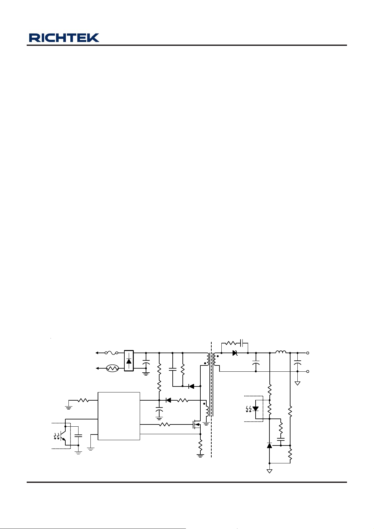
Typical Application Circuit
AC Mains
(90V to 265V)
RT
COMP
GND
VDD
R7730
GATE
CS
VO+
VO-
DS7730-00 May 2008 www.richtek.com
1
R7730
Preliminary
Ordering Information
R7730
Package Type
E : SOT-23-6
Operating Temperature Range
G : Green (Halogen Free with Commer cial Standard)
Note :
Richtek Green products are :
`RoHS compliant and compatible with the current requirements of IPC/JEDEC J-STD-020.
`Suitable for use in SnPb or Pb-free soldering processes.
`100% matte tin (Sn) plating.
Marking Information
For marking information, contact our sales re presentative directly or through a Richtek distributor located in your area,
otherwise visit our website for detail.
Pin Configurations
(TOP VIEW)
CSVDDGATE
4
56
23
1
COMP RT
GND
SOT-23-6
Note : There is no pin1 indicator on top mark for SOT-23-6 type, and pin 1 will be lower left pin when reading top mark from left
to right.
DS7730-00 May 2008www.richtek.com
2
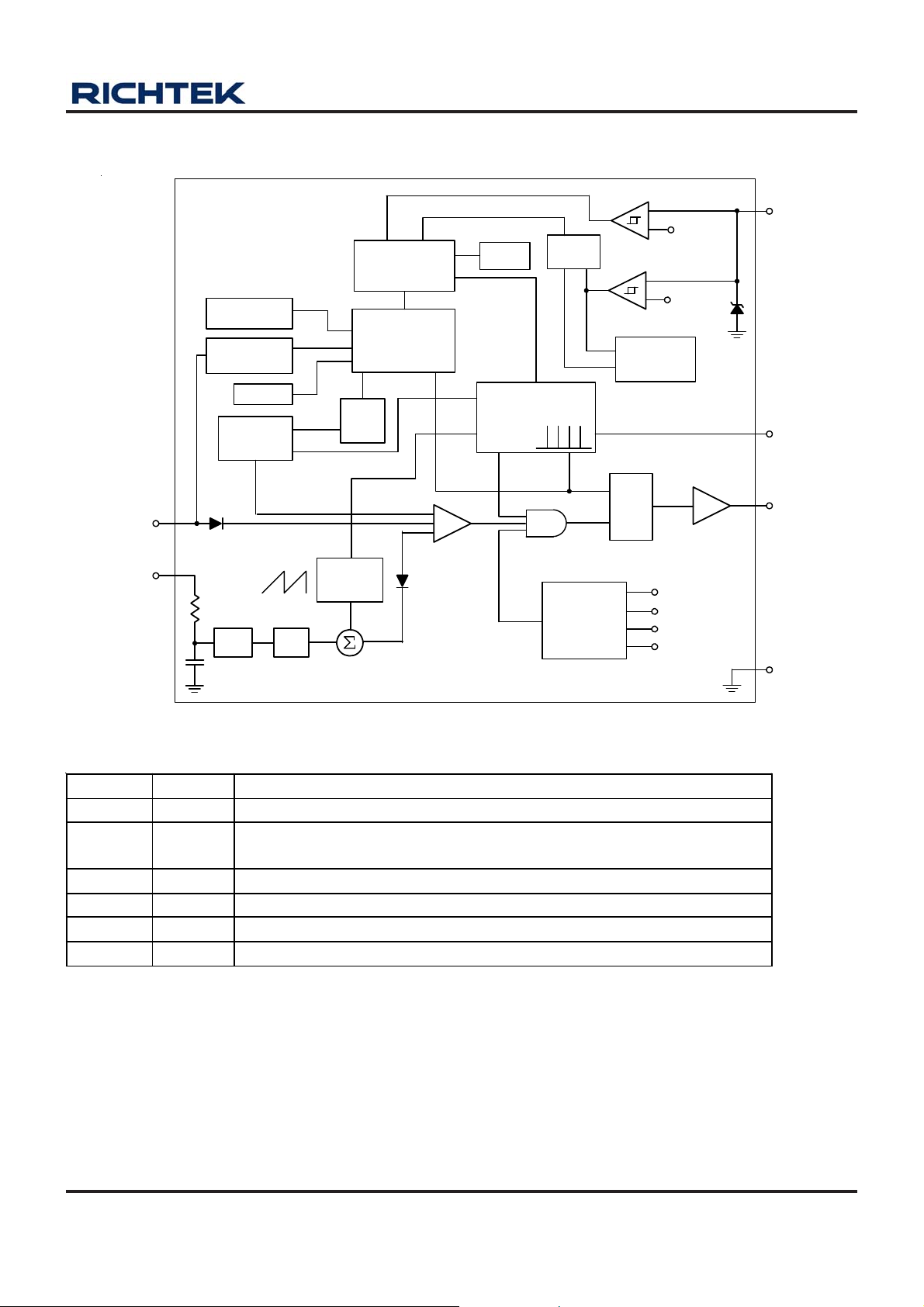
Function Block Diagram
Preliminary
R7730
COMP
CS
Brown out
sensing
COMP open
sensing
OLP
Constant
Power
LEB
X3
SS
Slope
Ramp
Shutdown
Logic
Counter
-
+
PWM
comparator
OTP
Dmax
Oscillator
POR
UVLO
Burst
Triple Mode
OVP
S
R
+
-
+
-
Bias &
Bandgap
Q
COMP
V
V
V
VDD
27V
14V/10V
RT
Soft
Driver
GATE
BURL
BURH
DD
GND
Functional Pin Description
Pin No. Pin Name Pin Function
1 GND Ground.
2 COMP
3 RT Set the switching frequency by connecting a resistor to GND.
4 CS Primary Current Sense Pin.
5 VDD IC Power Suppl y P in.
6 GATE Gate driver output to drive the external MOSFET.
DS7730-00 May 2008 www.richtek.com
Comparator Input Pin. By connecting a photo-coupler to this pin, the peak
current set point is adjusted accordingly to the output power requirement.
3
R7730
Preliminary
Absolute Maximum Ratings (Note 1)
z Supply Input V oltage, V
z GA TE Pin---------------------------------------------------------------------------------------------------------------- 20V
z FB, RT, COMP, CS Pin ---------------------------------------------------------------------------------------------- 6.5V
z I
------------------------------------------------------------------------------------------------------------------------- 10mA
DD
z Power Dissipation, P
------------------------------------------------------------------------------------------- 30V
DD
@ TA = 25°C
D
SOT-23-6 ---------------------------------------------------------------------------------------------------------------- 0.4W
z Package Thermal Re sistance (Note 4)
z SOT-23-6, θ
z Junction T emperature------------------------------------------------------------------------------------------------- 150°C
z Lead Temperature (Soldering, 10 sec.)--------------------------------------------------------------------------- 260°C
z Storage T emperature Range ---------------------------------------------------------------------------------------- −65°C to 150°C
z ESD Susceptibility (Note 2)
----------------------------------------------------------------------------------------------------------- 250°C/W
JA
HBM (Human Body Mode) ------------------------------------------------------------------------------------------ 4kV
MM (Ma chine Mode)-------------------------------------------------------------------------------------------------- 250V
Recommended Operating Conditions (Note 3)
z Supply Input V oltage, V
z Operating Frequency ------------------------------------------------------------------------------------------------- 50k to 130kHz
z Junction T emperature Range---------------------------------------------------------------------------------------- −40°C to 125°C
z Ambient T emperature Range---------------------------------------------------------------------------------------- −40°C to 85°C
------------------------------------------------------------------------------------------- 12V to 25V
DD
Electrical Characteristics
(V
= 15V, RT = 100kΩ, T
DD
Parameter Symbol Conditions Min Typ Max Unit
VDD Section
VDD Over Voltage Protection Level V
On Threshold Voltage V
VDD On/Off Hysteresis V
Start-up Current I
Operating Current I
VDD Hold-up Mode Hysteresis
E nding Lev el
VDD Hold-up Mode Entry Level V
VDD Clamp Voltage V
Oscillator Section (RT pin)
Normal PWM Frequency f
Maximum Duty Cycle D
Frequency Variation Versus VDD
Deviation
= 25°C, unless otherwise specified)
A
V
f
25.5 27 28.5 V
OVP
13 14 15 V
TH_ON
3 4 5 V
DD_hys
VDD = V
DD-ST
V
= 15V, RT = 100kΩ,
DD-OP
DD_hys
DD_Low
DD_Clamp
R
OS C
70 75 80 %
MAX
V
DV
DD
GATE = Open, V
V
V
< 1.6V -- 11.5 -- V
COMP
< 1.6V -- 11 -- V
COMP
-- 29 -- V
= 100kΩ 60 65 70 kHz
T
= 12V to 25V -- -- 2 %
VDD
– 0.1V -- 20 30 uA
TH_ON
COMP
= 2.5V
-- 1.1 2.2 mA
To be continued
DS7730-00 May 2008www.richtek.com
4

Preliminary
R7730
Parameter Symbol Conditions Min Typ Max Unit
Frequency Variation Versus
Temperature Deviation
f
T
DV
A
= −30°C to 105°C (Note 5) -- -- 5 %
COMP Input Section
Open Loop Voltage V
COMP Open-loop Protection Delay
cycles
Short Circuit COMP Current I
COMP-OP
T
OLP
ZERO
COMP pin Open 5 5.5 6 V
R
V
= 100kΩ -- 29 -- ms
T
= 0V -- 1.2 2.2 mA
COMP
Current-Sense Section
Peak Current Limitation V
Leading Edge Blanking Time T
0.65 0.7 0.75 V
CSTH
-- 420 520 ns
LEB
Propagation Delay Time TPD -- 100 -- ns
GATE Section
Rising Time TR V
Falling Time TF V
Gate Output Clamping Voltage V
Over Temperature Protection T
OTP Hysteresis T
Note 1. Stresses beyond those listed under “Absolute Maximum Ratings” may cause permanent damage to the device.
These are stress ratings only, and functional operation of the device at these or any other conditions beyond those
indicated in the operational sections of the specifications is not implied. Exposure to absolute maximum rating
conditions for extended periods may affect device reliability.
Note 2. Devices are ESD sensitive. Handling precaution is recommended.
Note 3. The device is not guaranteed to function outside its operating conditions.
Note 4. θ
Note 5. Guaranteed by design.
is measured in the natural convection at TA = 25°C on a low effective single layer thermal conductivity test board of
JA
JEDEC 51-3 thermal measurement standard.
VDD = 22V -- 12 -- V
clamp
-- 140 -- °C
OTP
OTP_hys
-- 30 -- °C
= 15V, CL = 1nF -- 250 350 ns
DD
= 15V, CL = 1nF -- 150 250 ns
DD
DS7730-00 May 2008 www.richtek.com
5

R7730
Preliminary
Typical Operating Characteristics
VTH vs. Temperature
15
14
13
(V)
12
DD
V
11
10
9
-40 -25 -10 5 20 35 50 65 80 95 110 125
Temperature
I
vs. Te m pe rature
1.55
1.50
1.45
(mA)
1.40
DD-OP
I
1.35
DD-OP
V
DD
= 27V
V
DD
V
= 11V
DD
(°C)
= 15V
V
TH_ON
V
TH_OFF
28
26
24
22
20
(uA)
18
DD-ST
I
16
14
12
10
-40 -15 10 35 60 85 110 135
63
V
62
61
V
60
(kHz)
OSC
f
59
DD
DD
= 11V
= 27V
V
DD
I
DD-ST
f
OSC
= 15V
vs. Temperature
Temperature
(°C)
vs. Temperature
V
= 13V
DD
1.30
V
= 2V, CL = 1nF
1.25
-40 -15 10 35 60 85 110 135
Temperature
D
vs. Temperature
80
79
78
77
76
(%)
75
MAX
74
D
73
72
71
70
-40 -20 0 20 40 60 80 100 120
MAX
Temperature
COMP
(°C)
(°C)
58
57
-40 -15 10 35 60 85 110 135
Temperature
V
vs. Temperature
5.50
5.45
5.40
5.35
(V)
5.30
COMP
V
5.25
5.20
5.15
-40 -20 0 20 40 60 80 100 120
COMP
Temperature
(°C)
COMP Open V oltage
(°C)
DS7730-00 May 2008www.richtek.com
6

Preliminary
R7730
Clamp Voltage vs. Temperature
13.0
12.5
12.0
11.5
Volt age (V)
11.0
10.5
10.0
-40 -15 10 35 60 85 110 135
Temperature
0.50
0.45
I
SUPPLY
vs. Temperature
VDD = 20V, CL = 1nF
(°C)
GATE (Rising/F alling) vs. Temperatur e
350
300
250
200
150
GATE (ns)
100
50
0
-40 -25 -10 5 20 35 50 65 80 95 110 125
13
12
11
Rising
Falling
Temperature
VOH vs. V
VDD = 20V, CL = 1nF
DD
(°C)
(mA)
0.40
SUPPLY
I
0.35
0.30
-40 -20 0 20 40 60 80 100 120
Temperature
V
600
575
550
525
500
(mV)
OL
V
475
450
425
400
11 12 13 14 15 16 17 18 19 20 21 22
OL
COMP Open
No Gate Output
I
SUPPLY
vs. V
DD
= I
(°C)
DD-OP
VDD (V)
I
SINK
− I
COMP
= 20mA
(mA)
SUPPLY
I
(V)
10
OH
V
9
8
I
7
11 12 13 14 15 16 17 18 19 20 21 22
SOURCE
VDD (V)
I
0.426
0.424
0.422
0.420
0.418
0.416
0.414
0.412
0.410
0.408
11 12 13 14 15 16 17 18 19 20 21 22
SUPPLY
vs. V
DD
V
COMP
No Gate Output
I
SUPPLY
Open
= I
VDD (V)
= 20mA
DD-OP
− I
COMP
DS7730-00 May 2008 www.richtek.com
7

R7730
Application Information
Preliminary
UVLO
Under voltage lockout (UVLO) block is to ensure V DD ha s
reached proper operation voltage before we enable the
whole IC blocks. T o provide better temperature coef ficient
and precise UVLO threshold voltage, the reference voltage
of hysteresis voltage (10V / 14V ) is from band-ga p block
directly . By this way , R7730 ca n operate more reli able in
different environments.
Oscillator
To guarantee precise frequency, it is trimmed to 5%
tolerance. It also generates slope compensation saw-tooth,
75% maximum duty cycle pulse and overload protection
slope. By adjusting resistor of RT pin according to the
following formula :
f (kHz) =
OSC
6500
T
R (k )Ω
It can typically operate between 50kHz to 130kHz. Note
that RT pin can’ t be short or open otherwise oscillator
will not operate.
Built-in Slope Compensation
Soft Start
During initial power on, especially at high line, current
spike is kind of unlimited by current limit. Therefore,
besides cycle-by-cycle current limiting, R7730 still
provides soft start function. It effectively suppresses the
start up current spike. As shown in the Figure 1 and
Figure 2, the start up VCS is about 0.3V lower than
competitor. Again, this will provide more relia ble operation
and possibility to use smaller current rating power
MOSFET.
V
CS
V
OUT
V
OUT
(2V/Div)
V
CS
(500mV/Div)
To reduce component count, slope compensation is
implemented by internal built-in saw-tooth. Since it’ s builtin, it’ s compromised between loop gain and sub-harmonic
reduction. In general design, it can ca ncel sub-harmonic
to 90Vac.
Leading Edge Blanking (LEB)
MOSFET Coss, secondary rectifier reverse recovery
current and gate driver sourcing current comprise initial
current spike. The spike will seriously disturb current mode
operation especially at light load and high line. R7730
provides built-in 420ns LEB to guarantee proper operation
in diverse design.
Noise Immunity
Current mode controller is very sensitive to noise. R7730
takes the adva ntages of RICHTEK long term experience
in designing high noise immunity current mode circuit and
layout. Also, we a mplify current sense sign al to compare
with feedback signal instea d of dividing feedba ck signal.
All the effort is to provide clea n and reli able current mode
operation.
Figure 1. Competitor
V
V
OUT
(2V/Div)
V
CS
OUT
V
CS
(500mV/Div)
Figure 2. R7730
Gate Driver
A totem pole gate driver is fine tuned to meet both EMI
and efficiency requirement in low power application. An
internal pull low circuit is activated after pretty low VDD to
prevent external MOSFET from accidentally turning on
during UVLO.
DS7730-00 May 2008www.richtek.com
8

Preliminary
R7730
Burst Triple-Mode
To fulfill green mode requirement, there are 3 operation
modes in R7730. Plea se also refer to Figure. 3 for details.
zz
z PWM Mode : For most of load condition, the circuit
zz
will run at traditional PWM current mode.
zz
z Burst Mode : During light load, switching loss will
zz
dominate the power efficiency calculation. This mode
is to cut switching loss. As shown in Figure 3, when
the output load gets light, feedback signal drops and
touches V
ceases to switching. After V
. Clock signal will be blanked a nd system
burL
drops and feedback
OUT
Normal
Operation
Load
VDD
V
DD_High
V
DD_Low
V
COMP
V
BURH
V
BURL
Light
Load
signal goes back to V
, switching will be resumed.
burH
Burst mode so far is widely used in low power
application because it’ s simple, reliable and will not
have any patent infringement issue.
zz
z VDD Holdup Mode : When the VDD drops down to
zz
VDD turn off threshold voltage, the system will be
shutdown. During shutdown period, controller does
nothing to any load cha nge and might cause V
OUT
down.
To avoid this, when VDD drops to a setting threshold,
11V, the hysteresis comparator will bypass PWM and
burst mode loop and force switching at a very low level
to supply energy to VDD.
No Load
(VDD Holdup Mode)
V
GATE
Figure 3. Burst Triple-Mode
Protection
R7730 provides fruitful protection functions that intend to
protect system from being damaged. All the protection
function can be listed a s below:
zz
z Cycle-by-Cycle Current Limiting : This is a basic but
zz
very useful function and it ca n be implemented ea sily in
current mode controller.
zz
z Overload Protection : Long time cycle-by-cycle
zz
current limiting will lead to system thermal stress. To
further protect system, system will be shutdown after
about 2048 clock cycles. It’ s about 30ms delay in
67kHz operation. After shutdown, system will resume
and behave a s hiccup. By proper startup resistor design,
thermal will be averaged to an a cceptable level over the
ON/OFF cycle of IC. This will la st until fault is removed.
zz
z Brownout Protection : During heavy load, this will
zz
trigger 30ms protection and shutdown the system. If
it’ s in light load condition, system will be shutdown
after V DD is running low a nd triggers UVLO.
zz
z OVP : Output voltage can be roughly sensed by VDD
zz
pin. If the sensed voltage reaches 27V threshold, system
will be shutdown after 20us deglitch delay .
zz
z Feedback Open and Opto Coupler Short : This will
zz
trigger OVP or 30ms delay protection. It depends on
which one occurs first.
zz
z OTP : Internal 110/140 °C hysteresis comparator will
zz
provide over temperature protection (OTP). OTP will not
shutdown system. It stops the system from switching
until the temperature is under 1 10°C. Meanwhile, if V D D
touches VDD turn off threshold voltage, system will
hiccup.
DS7730-00 May 2008 www.richtek.com
9

R7730
Outline Dimension
Preliminary
H
D
L
C
b
A
e
Dimensions In Millimeters Dimensions In Inches
Symbol
Min Max Min Max
A 0.889 1.295 0.031 0.051
A1 0.000 0.152 0.000 0.006
B 1.397 1.803 0.055 0.071
b 0.250 0.560 0.010 0.022
C 2.591 2.997 0.102 0.118
B
A1
D 2.692 3.099 0.106 0.122
e 0.838 1.041 0.033 0.041
H 0.080 0.254 0.003 0.010
L 0.300 0.610 0.012 0.024
Richtek Technology Corporation
Headquarter
5F, No. 20, Taiyuen Street, Chupei City
Hsinchu, Taiwan, R.O.C.
Tel: (8863)5526789 Fax: (8863)5526611
10
SOT-23-6 Surface Mount Package
Richtek Technology Corporation
Taipei Office (Marketing)
8F, No. 137, Lane 235, Paochiao Road, Hsintien City
Taipei County, Taiwan, R.O.C.
Tel: (8862)89191466 Fax: (8862)89191465
Email: marketing@richtek.com
DS7730-00 May 2008www.richtek.com

 Loading...