


Eclipse Series
RF Technology
rfinfo@rftechnology.com.au
October 2003 Revision 2
PA50 Amplifier
Operation and Maintenance Manual
This manual is produced by RF Technology Pty Ltd
10/8 Leighton Place, Hornsby NSW 2077 Australia
Copyright © 2001 RF Technology

Page 2 RF Technology PA50
CONTENTS CONTENTS
Contents
1 Operating Instructions 3
1.2 Front Panel Indicators 3
2 Internal Adjustments 3
3 Test Points 4
4 I/O Connections 4
5 Circuit Description 5
5.1 Driver Stage 5
5.2 Output Stage 5
5.3 Low Pass Filter 5
5.4 Bias Supply 5
5.5 Reflectometer 6
5.6 Metering Circuits 6
6 Specifications 7
6.1 Physical Configuration 7
6.2 Indicators and Test Points 7
6.3 Electrical Specifications 7
6.3.1 Power Requirements 7
A Engineers Drawings 9
B Parts List 10

RF Technology PA50 Page 3
1 OPERATING INSTRUCTIONS
1 Operating Instructions
The PA50 is part of the Eclipse range of modular base station equipment. It is a power
amplifier capable of delivering 120 Watts in the VHF frequency range. It is designed
to complement the T50 transmitter, and mounts in a standard Eclipse sub-rack.
1.2 Front Panel Indicators
PWR LED Power LED indicates that the PA50 is connected to a DC power source.
RFO LED RF Output LED indicates that the PA50 is being driven by the exciter
and RF Output is available at the antenna socket.
TEMP LED Temperature LED indicates that the output transistors are above 90
degrees. This is only an indication and not an alarm condition as the
exciter monitors the PA50 temperature at all times in order to keep
within safe operating limits.
2 Internal Adjustments
All internal adjustments are factory set and should not need to be changed under
normal conditions.
R238 Driver bias adjustment
R239 O/P Q101 bias adjustment
R240 O/P Q100 bias adjustment
R227 Forward power meter adjustment
R228 Reverse power meter adjustment
C209 Reflectometer balance adjustment
WARNING
Changes or modifications not expressly approved by RF
Technology could void your authority to operate this
equipment. Specifications may vary from those given in
this document in accordance with requirements of local
a
uthorities. RF Technology equipment is subject to
continual improvement and RF Technology reserves the
right to change performance and specification without
further notice.

Page 4 RF Technology PA50
3 Test Points 1 OPERATING INSTRUCTIONS
3 Test Points
These test points are provided on the PCB and the DB9 front panel connector for use
by maintenance personnel
TP100 and TP101 Driver drain current measurement. A multimeter placed across
these pins will indicate 1 volt for 1 amp of Q102 drain current
TP102 and TP103 O/P stage drain current measurement. A multimeter placed
across these pins will indicate 1 volt for 10 amps of Q100 and
Q101 drain current
TP200 PA Temperature reading. 1 volt indicates a temperature of 40
degrees. This reading deviates by 10mV per degree of change
TP203 Reverse voltage output from the reflectometer
TP204 Forward voltage output from the reflectometer
DB9 pin 1 GND
DB9 pin 2 O/P drain current
DB9 pin 3
DB9 pin 4 Reverse voltage
DB9 pin 5 +28V
DB9 pin 6 Driver drain current
DB9 pin 7
DB9 pin 8 Forward voltage
DB9 pin 9
4 I/O Connections
There are 3 I/O connectors on the rear panel with the following functions
25 pin connector DC power and exciter logic interface
Pin 1 2 3 4 14 15 16 17 GND
Pin 10 11 12 13 22 23 24 25 +28V
Pin 7 DATA-IO
Pin 19 CLK
Pin 20 CS
Pin 18 VREFB
Pin 6 Forward Volts
Pin 8 Reverse Volts
Pin 21 Temperature
BNC Connector: RF Input from exciter approximately1 Watt
N Connector: RF Output to antenna, up to 150 Watts

RF Technology PA50 Page 5
5 CIRCUIT DESCRIPTION 5.1 Driver Stage
5 Circuit Description
The following descriptions should be read as an aid to understanding the block and
schematic diagrams.
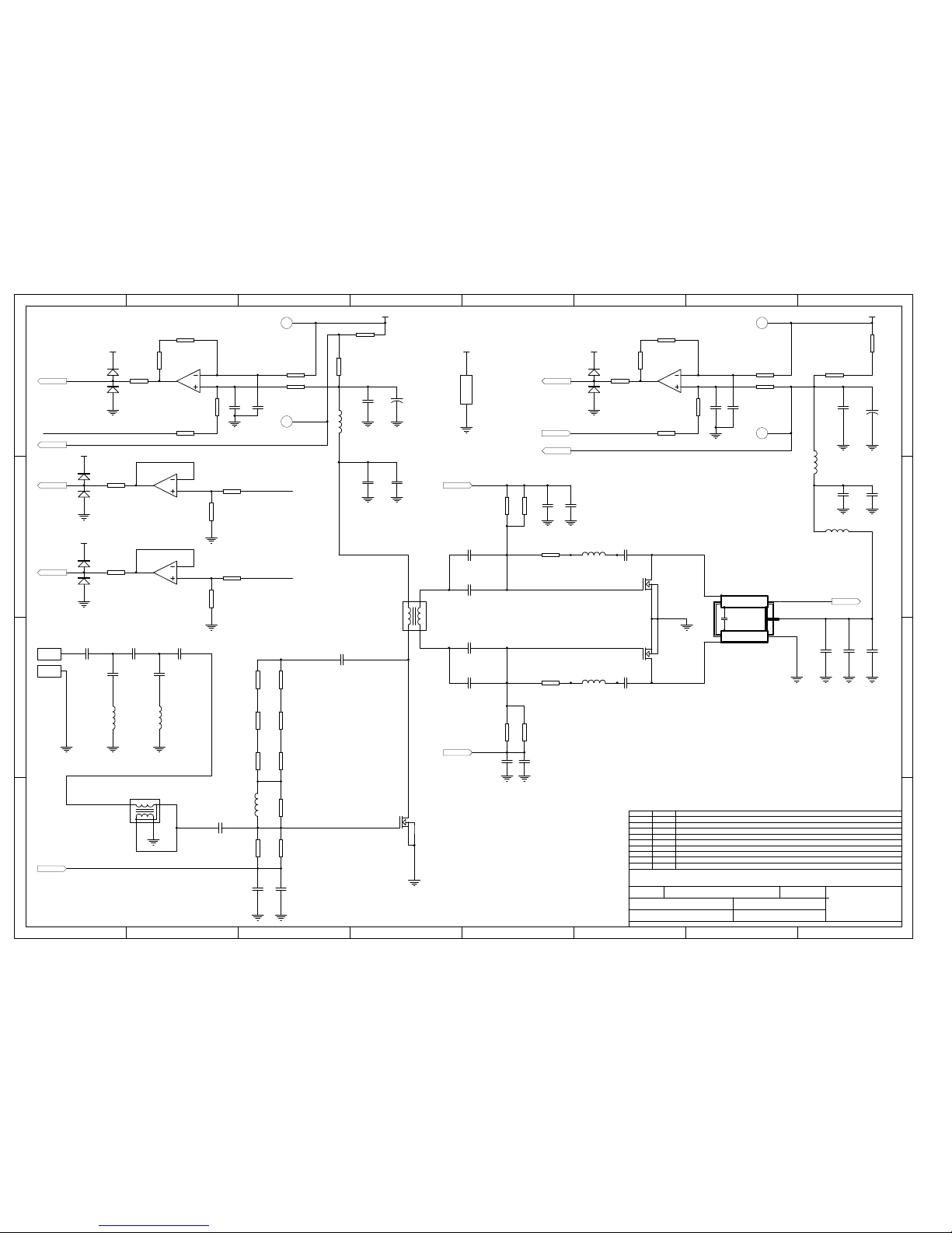
5.1 Driver Stage
The function of the driver stage is to transform the RF input signal from the exciter to
the appropriate levels and impedance required by the output stage. The RF input signal
is applied to the high pass filter ( C121, C130, C131, C132, C133, L102 and L106 ).
This filter suppresses any residual low frequency spurious that may be present at the
exciter output. T100 is used to transform the nominal 50 ohm output from the exciter
to match the input of Q102. A negative feedback network ( C120, R130, R132,
R131, R133, R125, R129, L107 and R124 ) is used to achieve a reasonably flat gain
across the frequency of operation and to match the drive level requirements of the
PA50 to the output level provided by the exciter. DC bias is applied to the gate of
Q102 via R120 and R121 and is decoupled by C106 and C116. The DC feed for Q102
drain is decoupled by L100, C112, C102, C100 and C118. T101 is used for impedance
matching between the driver and output stage and to provide a balanced feed for the
push-pull output stage
5.2 Output Stage
The output stage amplifies the 5 – 10 W from the driver to in excess of 150 W for final
delivery into the low pass filter. Q100 and 101 are driven in push-pull configuration
by the outputs of T101. L105, R126, C126 and L104 R127 C127 form negative
feedback paths in order to achieve a reasonably flat frequency response across the
frequency of operation. T102 is used to provide the DC feed via the centre tap in the
primary winding to Q100 and Q101. T102 also combines the balanced output of the
transistors into a single ended output as well as provide the necessary impedance
transformation from the transistors into a nominal 50 ohms. A small DC bias is
applied to the gates of Q100 and Q102 via R118, 119, 122 and 123 and decoupled by
C103, 113, 107 and 117. The DC feed to the transformer is decoupled by L103, L101,
C101, 119, 104, 114, 105, 115 and 128.
5.3 Low Pass Filter
The low pass filter attenuates spurious emissions to less than –86dBc.
5.4 Bias Supply
The function of the bias supplies is to provide a temperature compensated bias voltage
to the gates of Q100 Q101 and Q102 for adjustment to their quiescent currents. U205
and R213, R214 and R215 provide the bias voltages. U200D provides a decreasing
output voltage with increasing temperature. The resistive dividers R214, R229 and

Page 6 RF Technology PA50
5.5 Reflectometer 5 CIRCUIT DESCRIPTION
R213, R230 and R208, R215 provide the bias voltage to the transistors so that
quiescent current is maintained across the operating temperature range.
5.5 Reflectometer
The reflectometer provides an indication of load mismatch. A200 is a current
transformer with a single turn primary being passed through the centre of a toroid. The
multiturn secondary has an output voltage that is proportional to the current flowing in
the primary. The voltages appearing at the anodes of D205 and D206 are of equal
amplitude and opposite phase. A sample of the line voltage is applied to the junction
of the divider resistors R218 and R220. C209 is adjusted for equal amplitude with the
transformer. Since the transformer has 180 degree phase shifted outputs the
application of the line voltage will cause cancellation at D205 and addition at D206.
This phase relationship will change when a mismatch occurs resulting in an increase in
the voltage at D205. D205 and D206 rectify these voltages so that a DC level
proportional to the forward and reflected voltages are available for the metering
circuits. L200 provides a DC reference point for the diodes.
5.6 Metering Circuits
These circuits are included so that the exciter can interrogate the PA and read all the
vital operating levels. U203 is an A to D converter with the following inputs:
Reverse voltage
Forward voltage
Temperature
DC Input volts
O/P drain current
Driver drain current
Q100 bias voltage
Q101 bias voltage
Model identification jumpers
Forward and reverse voltages are supplied from the reflectometer outputs and factory
set to the correct levels by R227 and R228. U204 ( temperature sensor ) is mounted on
the same pad as the source lead of Q101 to provide a temperature reading of the O/P
transistor cases. DC Power Input voltage is provided by a resistive divider (R3 and
R4). The O/P drain current is provided by measuring the small voltage drop across
R113 and R128. Driver drain current is provided by measuring the small voltage drop
across R112 and R138. The bias voltages are read directly from the bias supplies. The
model identification is determined by the jumper settings of J203, 204 and 205.
PA50A 25 – 32 MHz J203 on, J204 and J205 off
PA50B 30 – 40 MHz J204 on, J203 and J205 off
PA50C 38 – 50 MHz J205 on, J203 and J204 off
U202 and associated components provide a 3 wire serial interface to allow the exciter
to interrogate the A to D converter. U200C is a comparator that switches the fan on

RF Technology PA50 Page 7
6 SPECIFICATIONS 6.1 Physical Configuration
when the temperature rises above 40 degrees C. U201D is a comparator that switches
the TEMP LED on when the temperature rises above 90 degrees C. Q203 samples the
line output RF voltage to turn on the RFO LED.
6 Specifications
The PA50 is designed for use with the T50 exciter to provide 20 to 150 Watts output.
Output power regulation is performed by the exciter as it continually monitors PA
performance. The exciter also monitors important levels such as temperature reverse
power and drain currents to keep them within operating limits.
6.1 Physical Configuration
The PA50 is designed to fit into a 19 inch rack mounted frame. The installed height is
4RU or 178mm and the depth is 350mm The amplifier is 125mm wide. An extruded
aluminium heatsink with vertical fins and an enclosed fan is used. The temperature
rise can be as high as 50 degrees depending on output power.
6.2 Indicators and Test Points
Power On Green LED
RF Power Yellow LED
Temperature 75 degrees + Red LED
Forward Power DB9 pin 8 and GND
Reverse Power DB9 pin 4 and GND
O/P Drain Current DB9 pins 2 and 5
Driver Drain Current DB9 pins 6 and 5
+28V DB9 pin 5
GND DB9 pin 1
6.3 Electrical Specifications
6.3.1 Power Requirements
Operating Voltage 26 to 30VDC ( available O/P power reduced below 26V
)
Current Drain Approx 10A at 28V and 100W O/P
Polarity Negative Ground
Frequency Range PA50A25 to 32MHz
PA50B 30 to 40MHz
PA50C 38 to 50MHz

Page 8 RF Technology PA50
6.3.1 Power Requirements 6 SPECIFICATIONS
Nominal Antenna Impedance: 50 ohms
Output Power: 20 to 100 Watts
Transmit Duty Cycle: 100W Continuous up to 60 degrees C ambient
Spurious Emissions: less than 0.25uW
Maximum Heatsink Temperature: 110 degrees C
Mismatch Protection: Protected from damage by control from the
exciter
Connectors: Antenna connector - N type female on rear panel
Power and exciter interface - DB25 Female on rear panel
RF Input - BNC female on rear panel
Test connector - DB9 female on front panel

RF Technology PA50 Page 9
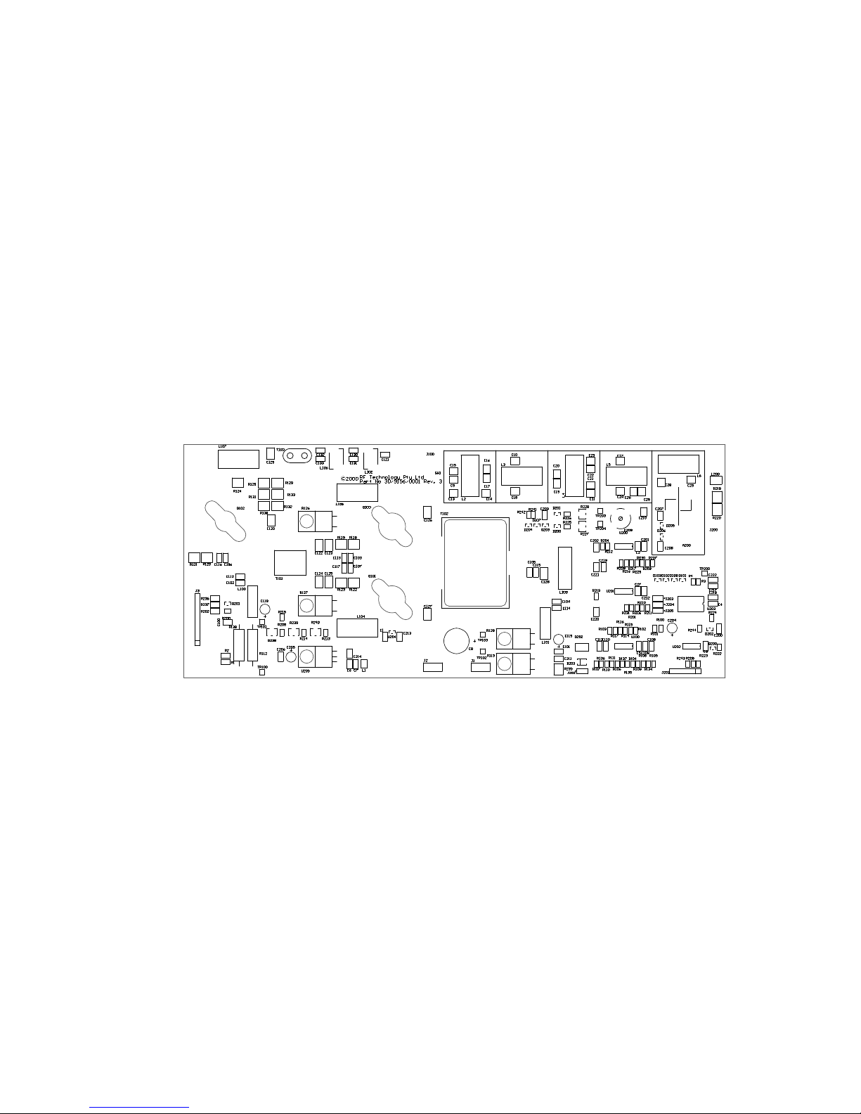
A ENGINEERING DRAWINGS
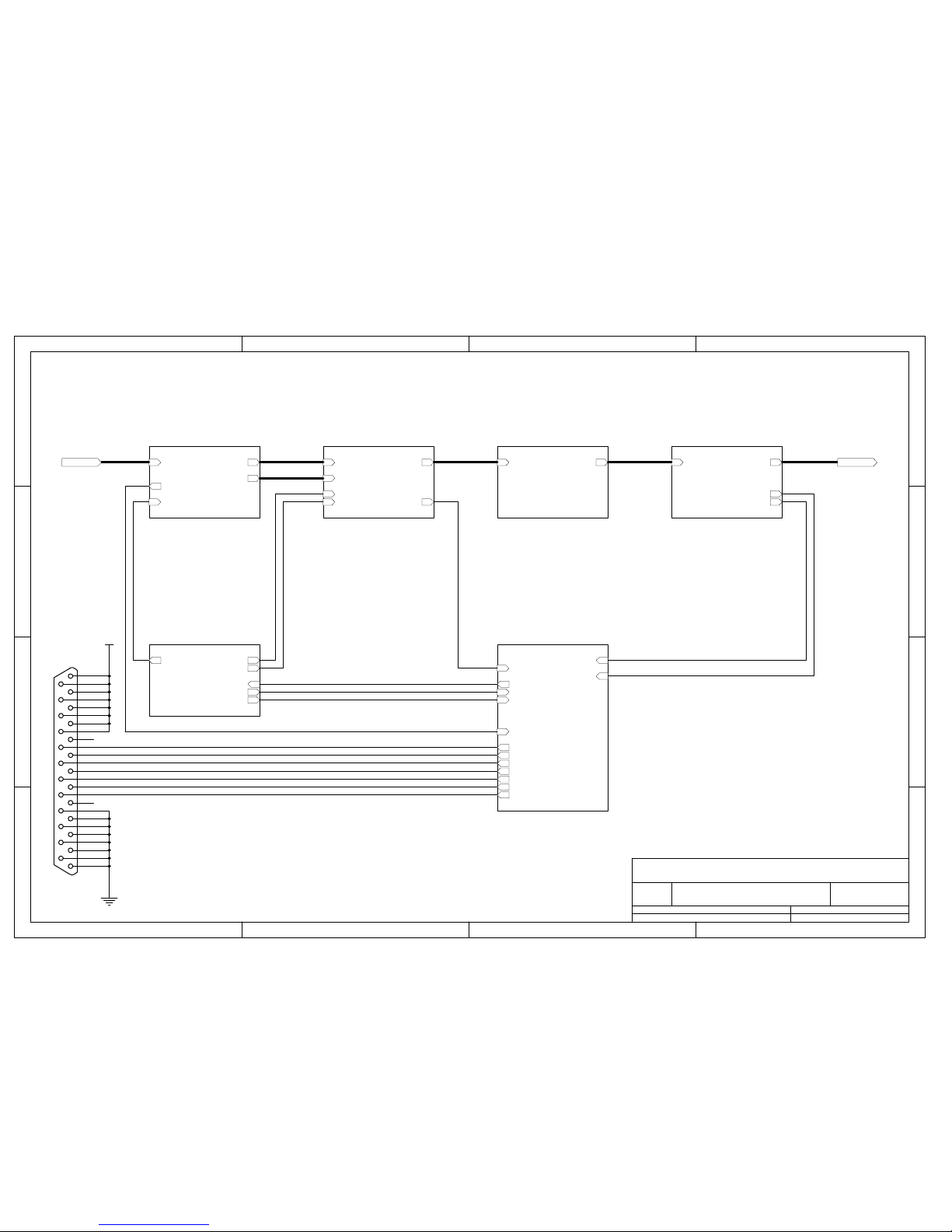
A Engineering Drawings
1. Block Diagram
2. Main PCB Schematics ( 3 sheets )

Page 10 RF Technology PA50
B PA50 PARTS LIST
B Parts List
Main PCB Assembly
Ref. Description Part Number
A200 Transformer Reflectometer 37/PA50/REFL
C1 Capacitor 100nF 10% 63V X7R 1206 46/3310/100N
C2 Capacitor 100nF 10% 63V X7R 1206 46/3310/100N
C3 Capacitor 100nF 10% 63V X7R 1206 46/3310/100N
C4 Capacitor 100nF 10% 63V X7R 1206 46/3310/100N
C5 Capacitor 100nF 10% 63V X7R 1206 46/3310/100N
C6 Capacitor 100nF 10% 63V X7R 1206 46/3310/100N
C7 Capacitor 1nF 5% 63V NPO 1206 46/3310/01N0
C8 Capacitor 330-560uF 35-50V low ESR
electrolytic 5mm pitch 41/200L/470U
C100 Capacitor 100nF 10% 63V X7R 1206 46/3310/100N
C101 Capacitor 100nF 10% 63V X7R 1206 46/3310/100N
C102 Capacitor 100nF 10% 63V X7R 1206 46/3310/100N
C103 Capacitor 100nF 10% 63V X7R 1206 46/3310/100N
C104 Capacitor 100nF 10% 63V X7R 1206 46/3310/100N
C105 Capacitor 100nF 10% 63V X7R 1206 46/3310/100N
C106 Capacitor 100nF 10% 63V X7R 1206 46/3310/100N
C107 Capacitor 100nF 10% 63V X7R 1206 46/3310/100N
C108 Capacitor 1nF 5% 63V NPO 1206 46/3310/01N0
C109 Capacitor 1nF 5% 63V NPO 1206 46/3310/01N0
C110 Capacitor 1nF 5% 63V NPO 1206 46/3310/01N0
C111 Capacitor 1nF 5% 63V NPO 1206 46/3310/01N0
C112 Capacitor 1nF 5% 63V NPO 1206 46/3310/01N0
C113 Capacitor 1nF 5% 63V NPO 1206 46/3310/01N0
C114 Capacitor 1nF 5% 63V NPO 1206 46/3310/01N0
C115 Capacitor 1nF 5% 63V NPO 1206 46/3310/01N0
C116 Capacitor 1nF 5% 63V NPO 1206 46/3310/01N0
C117 Capacitor 1nF 5% 63V NPO 1206 46/3310/01N0
C118 Capacitor 10uF +80/-20% 35V electrolytic
2.5mm pitch 41/200L/010U
C119 Capacitor 10uF +80/-20% 35V electrolytic
2.5mm pitch 41/200L/010U
C120 Capacitor 10nF 10% 50V NPO 1812 46/82N1/010N
C122 Capacitor 10nF 10% 50V NPO 1812 46/82N1/010N
C123 Capacitor 10nF 10% 50V NPO 1812 46/82N1/010N
C124 Capacitor 10nF 10% 50V NPO 1812 46/82N1/010N
C125 Capacitor 10nF 10% 50V NPO 1812 46/82N1/010N
C126 Capacitor 10nF 10% 50V NPO 1812 46/82N1/010N
C127 Capacitor 10nF 10% 50V NPO 1812 46/82N1/010N
C128 Capacitor 10nF 10% 50V NPO 1812 46/82N1/010N
C129 Capacitor 10nF 10% 50V NPO 1812 46/82N1/010N
C200 Capacitor 100nF 10% 63V X7R 1206 46/3310/100N
C201 Capacitor 100nF 10% 63V X7R 1206 46/3310/100N
C202 Capacitor 100nF 10% 63V X7R 1206 46/3310/100N

RF Technology PA50 Page 11
B PA50 PARTS LIST
Ref. Description Part Number
C203 Capacitor 100nF 10% 63V X7R 1206 46/3310/100N
C204 Capacitor 10uF +80/-20% 35V electrolytic
2.5mm pitch 41/200L/010U
C205 Capacitor 10uF +80/-20% 35V electrolytic
2.5mm pitch 41/200L/010U
C206 Capacitor 100nF 10% 63V X7R 1206 46/3310/100N
C207 Capacitor 68pF 5% 63V NPO 1206 46/3300/068P
C208 Capacitor 68pF 5% 63V NPO 1206 46/3300/068P
C209 Capacitor 6-100pF variable 49/3006/100P
C210 Capacitor 3p3F +/- 0.5pF 500V silver mica 1210 48/3003/03P3
C211 Capacitor 100nF 10% 63V X7R 1206 46/3310/100N
C212 Capacitor 100nF 10% 63V X7R 1206 46/3310/100N
C213 Capacitor 1nF 5% 63V NPO 1206 46/3310/01N0
C214 Capacitor 1nF 5% 63V NPO 1206 46/3310/01N0
C217 Capacitor 22pF 5% 63V NPO 1206 46/3300/022P
C218 Capacitor 22pF 5% 63V NPO 1206 46/3300/022P
C219 Capacitor 1nF 5% 63V NPO 1206 46/3310/01N0
C220 Capacitor 1nF 5% 63V NPO 1206 46/3310/01N0
C221 Capacitor 1nF 5% 63V NPO 1206 46/3310/01N0
C222 Capacitor 1nF 5% 63V NPO 1206 46/3310/01N0
D100 Diode BAV99 SOT-23 21/3010/AV99
D101 Diode BAV99 SOT-23 21/3010/AV99
D102 Diode BAV99 SOT-23 21/3010/AV99
D103 Diode BAV99 SOT-23 21/3010/AV99
D200 Diode BAV99 SOT-23 21/3010/AV99
D201 Diode BAV99 SOT-23 21/3010/AV99
D202 Diode ZRC400F03 4.096V reference 3%
100ppm SOT-23 29/VREF/0001
D203 Diode SM4004 Std recovery 50V !A SMA package 24/SMA1/4004
D204 Diode BAS21 SOT-23 21/000B/AS21
D205 Diode BAT17 SOT-23 21/3030/0017
D206 Diode BAT17 SOT-23 21/3030/0017
D207 Diode BZX84C10 10V zener 350mW 10% SOT-23 21/4050/C10V
J1 Connector 6.35mm QC Vertical Tab 35/0635/0001
J2 Connector 6.35mm QC Vertical Tab 35/0635/0001
J3 Connector 10 way female 35/2501/0010
J201 Connector 6 way male 35/2501/0006
J202 Connector 2 way male locking 35/2505/0002
J203 Connector 2 way male 35/2501/0002
J204 Connector 2 way male 35/2501/0002
J205 Connector 2 way male 35/2501/0002
L1 Inductor 3u3H 20% >100mA 1008 37/3320/P101
L100 Inductor Ferrite beads 3x4x1 4S2 37/1022/0001
L101 Inductor Ferrite beads 3x4x1 4S2 37/1022/0001
L103 Inductor 8 turns on 20mm toroid 37/PA50/0003
L104 Inductor 315nH 11 turns CW 6.35mm ID 37/0635/1511
L105 Inductor 315nH 11 turns CW 6.35mm ID 37/0635/1511
L107 Inductor 247nH 9 turns CW 6.35mm ID 37/0635/1509
L200 Inductor 33uH 10% >100mA 1812 37/3320/P102
Q100 Transistor MRF174 RF Power mosfet 27/3020/MRF174

Page 12 RF Technology PA50
B PA50 PARTS LIST
Ref. Description Part Number
Q101 Transistor MRF174 RF Power mosfet 27/3020/MRF174
Q102 Transistor MRF136 RF Power mosfet 27/3020/MRF136
Q200 Transistor MMBT3904 NPN SOT-23 27/3020/3904
Q201 Transistor MMBT3904 NPN SOT-23 27/3020/3904
Q202 Transistor NDT3055 n-ch mosfet SOT-223 27/3020/3055
R1 Resistor 1K2 5% 1206 51/3380/01K2
R2 Resistor 1K2 5% 1206 51/3380/01K2
R3 Resistor 15K 1% 200ppm 0805 51/8511/015K
R4 Resistor 1K2 1% 200ppm 0805 51/8511/01K2
R100 Resistor 470R 1% 200ppm 0805 51/8511/470R
R101 Resistor 470R 1% 200ppm 0805 51/8511/470R
R102 Resistor 470R 1% 200ppm 0805 51/8511/470R
R103 Resistor 470R 1% 200ppm 0805 51/8511/470R
R104 Resistor 15K precision 0.5% 50ppm 0805 51/85P1/015K
R105 Resistor 15K precision 0.5% 50ppm 0805 51/85P1/015K
R106 Resistor 15K precision 0.5% 50ppm 0805 51/85P1/015K
R107 Resistor 15K precision 0.5% 50ppm 0805 51/85P1/015K
R108 Resistor 15K precision 0.5% 50ppm 0805 51/85P1/015K
R109 Resistor 15K precision 0.5% 50ppm 0805 51/85P1/015K
R110 Resistor 15K precision 0.5% 50ppm 0805 51/85P1/015K
R111 Resistor 15K precision 0.5% 50ppm 0805 51/85P1/015K
R112 Resistor 1R 10% 3W axial wirewound 51/1053/001R
R113 Resistor 0R05 20W T0-220 51/T220/0R05
R114 Resistor 100K 1% 200ppm 0805 51/8511/100K
R115 Resistor 100K 1% 200ppm 0805 51/8511/100K
R116 Resistor 100K 1% 200ppm 0805 51/8511/100K
R117 Resistor 100K 1% 200ppm 0805 51/8511/100K
R118 Not Fitted
R119 Resistor 1K5 5% 1W 200ppm 1218 51/8251/01K5
R120 Resistor 100R 5% 1W 200ppm 1218 51/8251/0100
R121 Resistor 100R 5% 1W 200ppm 1218 51/8251/0100
R122 Not Fitted
R123 Resistor 1K5 5% 1W 200ppm 1218 51/8251/01K5
R124 Resistor 220R 5% 1W 200ppm 1218 51/8251/0220
R125 Resistor 150R 5% 1W 200ppm 1218 51/8251/0150
R126 Resistor 100R 20W T0-220 51/T220/0100
R127 Resistor 100R 20W T0-220 51/T220/0100
R128 Resistor 0R05 20W T0-220 51/T220/0R05
R129 Resistor 150R 5% 1W 200ppm 1218 51/8251/0150
R130 Resistor 150R 5% 1W 200ppm 1218 51/8251/0150
R131 Resistor 150R 5% 1W 200ppm 1218 51/8251/0150
R132 Resistor 150R 5% 1W 200ppm 1218 51/8251/0150
R133 Resistor 150R 5% 1W 200ppm 1218 51/8251/0150
R134 Resistor 15K precision 0.5% 50ppm 0805 51/85P1/015K
R135 Resistor 15K precision 0.5% 50ppm 0805 51/85P1/015K
R136 Resistor 15K precision 0.5% 50ppm 0805 51/85P1/015K
R137 Resistor 15K precision 0.5% 50ppm 0805 51/85P1/015K
R138 Resistor 2R7 10% 3W axial wirewound 51/1053/02R7
R200 Resistor 15K 1% 200ppm 0805 51/8511/015K
R201 Resistor 6K8 1% 200ppm 0805 51/8511/06K8

RF Technology PA50 Page 13
B PA50 PARTS LIST
Ref. Description Part Number
R202 Resistor 1K5 5% 1206 51/3380/01K5
R203 Resistor 39K 1% 200ppm 0805 51/8511/039K
R204 Resistor 39K 1% 200ppm 0805 51/8511/039K
R208 Resistor 68K 1% 200ppm 0805 51/8511/068K
R209 Resistor 4K7 1% 200ppm 0805 51/8511/04K7
R210 Resistor 10K 1% 200ppm 0805 51/8511/010K
R211 Resistor 10K 1% 200ppm 0805 51/8511/010K
R212 Resistor 10K 1% 200ppm 0805 51/8511/010K
R213 Resistor 10K 1% 200ppm 0805 51/8511/010K
R214 Resistor 10K 1% 200ppm 0805 51/8511/010K
R215 Resistor 10K 1% 200ppm 0805 51/8511/010K
R216 Resistor 100K 1% 200ppm 0805 51/8511/100K
R217 Resistor 100K 1% 200ppm 0805 51/8511/100K
R218 Resistor 22R 5% 1W 200ppm 1218 51/8251/0022
R219 Resistor 1K 1% 200ppm 0805 51/8511/01K0
R222 Resistor 4K7 1% 200ppm 0805 51/8511/04K7
R223 Resistor 100R 1% 200ppm 0805 51/8511/100R
R224 Resistor 560R 1% 200ppm 0805 51/8511/560R
R225 Resistor 470R 1% 200ppm 0805 51/8511/470R
R226 Resistor 470R 1% 200ppm 0805 51/8511/470R
R227 Resistor 22R 5% 1W 200ppm 1218 51/8251/0022
R228 Resistor 100K variable 11 turn 4mm gull wing 53/SMV1/100K
R238 Resistor 100K variable 11 turn 4mm gull wing 53/SMV1/100K
R235 Resistor 33R 5% 1W 200ppm 1218 51/8251/0033
R236 Resistor 4K7 5% 1206 51/3380/04K7
R237 Resistor 4K7 5% 1206 51/3380/04K7
R238 Resistor 1K variable 11 turn 4mm gull wing 53/SMV1/001K
R239 Resistor 1K variable 11 turn 4mm gull wing 53/SMV1/001K
R240 Resistor 1K variable 11 turn 4mm gull wing 53/SMV1/001K
R242 Resistor 1M 1% 200ppm 0805 51/8511/01M0
R243 Resistor 10K 1% 200ppm 0805 51/8511/010K
R244 Resistor 4K7 1% 200ppm 0805 51/8511/04K7
T100 Transformer 4:1 Unbalanced 37/PA50/0004
T101 Transformer 1:1 Balun 37/PA50/0004
T102 Transformer 1:9 RF Output 37/PA50/0001
U100 IC LM224 Quad op-amp SO-14 29/000L/M224
U200 IC LM224 Quad op-amp SO-14 29/000L/M224
U201 IC LM224 Quad op-amp SO-14 29/000L/M224
U202 IC 74HC125 buffer SO-14 26/2030/C125
U203 IC TLC542 8 bit A/D converter SO-20 29/00TL/C542
U204 IC LM61 Temperature sensor SOT-23 29/0001/LM61
U205 IC LM7805CT Regulator TO-220 25/2040/85CT
Frequency Dependant Parts PA50A ( 25 – 32 MHz )
C9 Capacitor 27pF 1% 500V Silver Mica 1210 48/3003/027P
C10 Capacitor 33pF 1% 500V Silver Mica 1210 48/3003/033P
C11 Capacitor 18pF 1% 500V Silver Mica 1210 48/3003/018P
C12 Capacitor 3p3F +/- 0.1pF 500V Silver Mica 1210 48/3003/03P3
C13 Capacitor 56pF 1% 500V Silver Mica 1210 48/3003/056P

Page 14 RF Technology PA50
B PA50 PARTS LIST
Ref. Description Part Number
C14 Capacitor 18pF 1% 500V Silver Mica 1210 48/3003/018P
C15 Capacitor 27pF 1% 500V Silver Mica 1210 48/3003/027P
C16 Capacitor 100pF 1% 500V Silver Mica 1210 48/3003/100P
C17 Capacitor 33pF 1% 500V Silver Mica 1210 48/3003/033P
C18 Not Fitted
C19 Capacitor 100pF 1% 500V Silver Mica 1210 48/3003/100P
C20 Capacitor 56pF 1% 500V Silver Mica 1210 48/3003/056P
C21 Not Fitted
C22 Capacitor 100pF 1% 500V Silver Mica 1210 48/3003/100P
C23 Capacitor 68pF 1% 500V Silver Mica 1210 48/3003/068P
C24 Capacitor 3p3F +/- 0.1pF 500V Silver Mica 1210 48/3003/03P3
C25 Capacitor 100pF 1% 500V Silver Mica 1210 48/3003/100P
C26 Capacitor 10pF +/- 0.1pF 500V Silver Mica 1210 48/3003/010P
C28 Capacitor 68pF 1% 500V Silver Mica 1210 48/3003/068P
C29 Capacitor 68pF 1% 500V Silver Mica 1210 48/3003/068P
C121 Capacitor 120pF 5% 63V NPO 1206 46/3300/120P
C130 Capacitor 470pF 5% 63V NPO 1206 46/3300/470P
C131 Capacitor 100pF 5% 63V NPO 1206 46/3300/100P
C132 Capacitor 120pF 5% 63V NPO 1206 46/3300/120P
C133 Capacitor 220pF 5% 63V NPO 1206 46/3300/220P
C1000 Capacitor 180pF 1% 500V Silver Mica 1210 48/3003/180P
C1001 Not Fitted
L2 Inductor 184nH 7 turns CW 6.35mm ID 37/0635/1507
L3 Inductor 247nH 9 turns CW 6.35mm ID 37/0635/1509
L4 Inductor 247nH 10 turns CW 6.35mm ID 37/0635/1510
L5 Inductor 284nH 10 turns CW 6.35mm ID 37/0635/1510
L6 Inductor 247nH 9 turns CW 6.35mm ID 37/0635/1509
L102 Inductor 307nH Coilcraft Maxispring 37/MAXI/307N
L106 Inductor 558nH Coilcraft Maxispring 37/MAXI/558N
Frequency Dependant Parts PA50B ( 30 – 40 MHz )
C9 Capacitor 33pF 1% 500V Silver Mica 1210 48/3003/033P
C10 Capacitor 27pF 1% 500V Silver Mica 1210 48/3003/027P
C11 Capacitor 12pF 1% 500V Silver Mica 1210 48/3003/012P
C12 Capacitor 5p6F +/- 0.1pF 500V Silver Mica 1210 48/3003/05P6
C13 Capacitor 47pF 1% 500V Silver Mica 1210 48/3003/047P
C14 Capacitor 15pF 1% 500V Silver Mica 1210 48/3003/015P
C15 Capacitor 12pF 1% 500V Silver Mica 1210 48/3003/012P
C16 Capacitor 100pF 1% 500V Silver Mica 1210 48/3003/100P
C17 Capacitor 12pF 1% 500V Silver Mica 1210 48/3003/012P
C18 Capacitor 4p7F +/- 0.1pF 500V Silver Mica 1210 48/3003/04P7
C19 Capacitor 82pF 1% 500V Silver Mica 1210 48/3003/082P
C20 Capacitor 47pF 1% 500V Silver Mica 1210 48/3003/047P
C21 Capacitor 4p7F +/- 0.1pF 500V Silver Mica 1210 48/3003/04P7
C22 Capacitor 100pF 1% 500V Silver Mica 1210 48/3003/100P
C23 Capacitor 47pF 1% 500V Silver Mica 1210 48/3003/047P
C24 Not Fitted
C25 Capacitor 82pF 1% 500V Silver Mica 1210 48/3003/082P
C26 Capacitor 10pF +/- 0.1pF 500V Silver Mica 1210 48/3003/010P

RF Technology PA50 Page 15
B PA50 PARTS LIST
Ref. Description Part Number
C28 Capacitor 100pF 1% 500V Silver Mica 1210 48/3003/100P
C29 Capacitor 100pF 1% 500V Silver Mica 1210 48/3003/100P
C121 Capacitor 82pF 5% 63V NPO 1206 46/3300/082P
C130 Capacitor 330pF 5% 63V NPO 1206 46/3300/330P
C131 Capacitor 100pF 5% 63V NPO 1206 46/3300/100P
C132 Capacitor 100pF 5% 63V NPO 1206 46/3300/100P
C133 Capacitor 180pF 5% 63V NPO 1206 46/3300/180P
C1000 Capacitor 150pF 1% 500V Silver Mica 1210 48/3003/150P
C1001 Not Fitted
L2 Inductor 150nH 6 turns CW 6.35mm ID 37/0635/1506
L3 Inductor 184nH 7 turns CW 6.35mm ID 37/0635/1507
L4 Inductor 215nH 8 turns CW 6.35mm ID 37/0635/1508
L5 Inductor 215nH 8 turns CW 6.35mm ID 37/0635/1508
L6 Inductor 215nH 8 turns CW 6.35mm ID 37/0635/1508
L102 Inductor 307nH Coilcraft Maxispring 37/MAXI/307N
L106 Inductor 491nH Coilcraft Maxispring 37/MAXI/491N
Frequency Dependant Parts PA50C ( 38 – 50 MHz )
C9 Capacitor 15pF 1% 500V Silver Mica 1210 48/3003/015P
C10 Capacitor 12pF 1% 500V Silver Mica 1210 48/3003/012P
C11 Capacitor 12pF 1% 500V Silver Mica 1210 48/3003/012P
C12 Capacitor 3p9F +/- 0.1pF 500V Silver Mica 1210 48/3003/03P9
C13 Capacitor 47pF 1% 500V Silver Mica 1210 48/3003/047P
C14 Not Fitted
C15 Capacitor 18pF 1% 500V Silver Mica 1210 48/3003/018P
C16 Capacitor 82pF 1% 500V Silver Mica 1210 48/3003/082P
C17 Capacitor 4p7F +/- 0.1pF 500V Silver Mica 1210 48/3003/04P7
C18 Capacitor 12pF 1% 500V Silver Mica 1210 48/3003/012P
C19 Capacitor 100pF 1% 500V Silver Mica 1210 48/3003/100P
C20 Not Fitted
C21 Not Fitted
C22 Capacitor 100pF 1% 500V Silver Mica 1210 48/3003/100P
C23 Capacitor 12pF 1% 500V Silver Mica 1210 48/3003/012P
C24 Not Fitted
C25 Capacitor 33pF 1% 500V Silver Mica 1210 48/3003/033P
C26 Capacitor 39pF +/- 0.1pF 500V Silver Mica 1210 48/3003/039P
C28 Capacitor 68pF 1% 500V Silver Mica 1210 48/3003/068P
C29 Capacitor 68pF 1% 500V Silver Mica 1210 48/3003/068P
C121 Capacitor 82pF 5% 63V NPO 1206 46/3300/082P
C130 Capacitor 180pF 5% 63V NPO 1206 46/3300/180P
C131 Capacitor 68pF 5% 63V NPO 1206 46/3300/068P
C132 Capacitor 68pF 5% 63V NPO 1206 46/3300/068P
C133 Capacitor 180pF 5% 63V NPO 1206 46/3300/180P
C1000 Capacitor 100pF 1% 500V Silver Mica 1210 48/3003/100P
C1001 Not Fitted
L2 Inductor 121nH 5 turns CW 6.35mm ID 37/0635/1505
L3 Inductor 150nH 6 turns CW 6.35mm ID 37/0635/1506
L4 Inductor 184nH 7 turns CW 6.35mm ID 37/0635/1507
L5 Inductor 184nH 7 turns CW 6.35mm ID 37/0635/1507

Page 16 RF Technology PA50
B PA50 PARTS LIST
Ref. Description Part Number
L6 Inductor 150nH 6 turns CW 6.35mm ID 37/0635/1506
L102 Inductor 246nH Coilcraft Maxispring 37/MAXI/246N
L106 Inductor 380nH Coilcraft Maxispring 37/MAXI/380N
Front Panel PCB
R1 Resistor 100R 5% 0.25W axial 51/1040/0100
D1 Diode LED Yellow RA 21/1010/LEDY
D2 Diode LED Red RA 21/1010/LEDR
D3 Diode LED Green RA 21/1010/LEDG
J1 Connector 10 way header 35/2501/0010
J2 Connector DB9/F RA PCB mount 35/5012/009F
1 2 3 4
A
B
C
D
4321
D
C
B
A
Title
Number RevisionSize
A4
Date: 21-Feb-2002 Sheet of
File: C:\Program Files\Design Explorer 99 SE\rft\PA50.ddbDrawn By:
Driver Bias
RF Input Q100 Drive
Q101 Drive
Driver Drain Current
Q101 Drive
Q100 Drive
Q100 Bias
Q101 Bias O/P Drain current
Unfiltered RF Unfiltered RF Filtered RF Filtered RF RF Output
Fwd Volts
Rev Volts
Driver Bias
Q101 Bias
Q100 Bias
Temperature Compensation
Q100 Bias voltmeter
Q101 Bias voltmeter
Temperature Compensation
Driver Drain Current
Q101 Bias voltmeter
Q100 Bias voltmeter
O/P Drain current
Rev Volts
Fwd Volts
Temperature
Reverse Volts
CS
DATA-IO
CLK
Forward Volts
VREFB
Driver Stage O/P Stage Low Pass Filter Reflectometer
Bias Supply Metering
RF Input RF Ouput
1
14
2
15
3
16
4
17
5
18
6
19
7
20
8
21
9
22
10
23
11
24
12
25
13
J?
DB25
+28V
Temperature
Reverse Volts
CS
DATA-IO
CLK
Forward Volts
VREFB
PA50 Block Diagram

1 2 3 4 5 6 7 8
A
B
C
D
87654321
D
C
B
A
R238
1K
R215
10K
C206
100nF
R214
10K
BIAS-OP2
BIAS-DRV
C210
3p3F
L200
33uH
D205
BAT17
D206
BAT17
C207
68pF
C208
68pF
C209
6-100pF
A200
F/R_COAX
AIN0
1
AIN1
2
AIN2
3
AIN3
4
AIN4
5
AIN5
6
AIN6
7
AIN7
8
AIN8
9
AIN9
11
AIN10
12
GND
10
VCC
20
REF-
13
REF+
14
CS
15
DO
16
DI
17
CLK
18
EOC
19
U203
TLC542
1
4
10
13
2
5
9
12
3
6
8
11
7 14
U202
74HC125
R205
10K
R222
4.7K
+5V
DATA-IO
CLK
CS
+5V
+5V
R213
10K
BIAS-OP1
+5V
R204
39K
R212
10K C202
100nF
+5V
Q202
NDT3055
1
2
J202
CON2
3 3
PA50 100W Power Amplifier
D
21-Feb-2002 00:02:56
C:\Program Files\Design Explorer 99 SE\rft\PA50.ddb - HFPA_Support.Sch
Title
Size: Number:
Print Date:
File:
Revision:
Sheet of
A3
RF Technology Pty Ltd
Unit 10, 8 Leighton Place
Hornsby, NSW 2077
AustraliaRev. Release Date: Originator:
Rev No. ECO No. Description of Change
RF-FILT
R216
100K
R217 100K
+5V
R203
39K
R207
10K
R230
47K
R229
47K
C201
100nF
R242
1M
R202
1.5K
C203
100nF
R200
15K
R236
4.7K
+5V
TempLED
RFOLED
R225
1K
R226
1K
J204 LINK
J205 LINK
J203 LINK
CurrSense
DrvSense
B1Sense
B2Sense
PwrSense
R211
10K
R210
10K
R206
10K
+5V
R224
560R
R223
100R
S1
S2
S0
S1
S2
S0
S1
S2
S0
S[0..2]
Forward & Reflected Power Meter
Fan Switch and Temperature Indicator
Measurement Interface
Bias Voltage Temperature Compensation
Bias Voltage Adjustments
RF Output Indicator
Identification Jumpers
V+
1
Vo
2
GND
3
U204
LM61
+5V
+5V
+5V
+
C204
10uF
R237
4.7K
R241
180K
C200100nF
J200
COAX-PAD
D203
SM4004
D207
BZX84C10
D202
ZRC400F03
Q201
MMBT3904
Q200
3904
Q203
FMMT38C
D204
BAS21
R239
1K
R240
1K
R227
100K
R228
100K
R218
22R
R220
22R
Vin
1
GND
2
Vout
3
U205
LM7805CT
+
C205
10uF
+28F
2
3
1
U200A
LM224
5
6
7
U200B
LM224
V+
4
V-
11
U200E
LM224
14
13
12
U200D
LM224
9
10
8
U200C
LM224
V+
4
V-
11
U201E
LM224
2
3
1
U201A
LM224
5
6
7
U201B
LM224
9
10
8
U201C
LM224
14
13
12
U201D
LM224
+28F
R201
6K8
R231
56K
R243
10K
R244
4.7K
+5V
D200
BAV99
D201
BAV99
+28V
R235
33R
Pwr-Rev
Pwr-Fwd
C211
100nF
RF-UNFILT
R208
68K
C213
1nF
C212
100nF
C214
1nF
TP203
TEST-POINT
TP204
TEST-POINT
TP200
TEST-POINT
C219 1nF
C221
1nF
R209
4.7K
R219
1K
C220
1nF
C222
1nF
VREFB
C218
22pF
C217
22pF
1
2
3
4
5
6
J201
CON6
Pwr-Fwd
Pwr-Rev
Pwr-Rev
Pwr-Fwd
Temperature
1 2 3 4 5 6 7 8
A
B
C
D
87654321
D
C
B
A
C126
22nF
C127
22nF
R126
100R
R127
100R
BIAS-OP2
C129
22nF
R125
150R
C120
22nF
BIAS-DRV
L101
BEADS
C114
1nF
C104
100nF
C101
100nF
+
C119
10uF
L103
TOROID-20MM
C115
1nF
C105
100nF
R121
100R
C106
100nF
C116
1nF
R123
1K2
C107
100nF
C117
1nF
C123
22nF
C124
22nF
R118
NF
C103
100nF
C113
1nF
BIAS-OP1
R113
0R05
O/P-DCurr
RF-UNFILT
2 3
PA50 100W Power Amplifier
D
21-Feb-2002 00:01:56
C:\Program Files\Design Explorer 99 SE\rft\PA50.ddb - HFPA_Main.Sch
Title
Size: Number:
Print Date:
File:
Revision:
Sheet of
A3
RF Technology Pty Ltd
Unit 10, 8 Leighton Place
Hornsby, NSW 2077
AustraliaRev. Release Date: Originator:
Rev No. ECO No. Description of Change
C122
22nF
C125
22nF
+28V
+28F
CurrSense
R101
470R
+5V
R102
470R
R103
470R
B1Sense
B2Sense
R114
100K
R116
100K
R115
100K
R117
100K
BIAS-OP1
BIAS-OP2
BIAS-DRV
BIAS-OP1
BIAS-OP2
Driver Stage
Output Stage
Bias Voltage Measurement Interface
Drain Current Meter
L100
BEADS
C112
1nF
C102
100nF
C100
100nF
+
C118
10uF
R112
1R0
+28V
R100
470R
+5V
Drain Current Meter
+5V
+5V
DrvSense
Drv-DCurr
RF-UNFILT
J100
COAX-PAD
C108
1nF
C109
1nF C110
1nF
C111
1nF
T102
RF-TFORMER-9:1
T100
4:1-UNBAL
R124
220R
R120
100R
R119
1K2
T101
1:1-BALUN
R122
NF
C128
22nF
Q102
MRF136
Q100
MRF174
Q101
MRF174
2
3
1
U100A
LM224
V+
4
V-
11
U100E
LM224
9
10
8
U100C
LM224
14
13
12
U100D
LM224
5
6
7
U100B
LM224
D100
BAV99
D101
BAV99
D102
BAV99
D103
BAV99
R106
21K
R107
21K
R104
21K
R105
21K
R108
21K
R109
21K
R110
21K
R111
21K
R128
0R05
C121
see table
C131
see table
C133
see table
C130
see table
C132
see table
L102
see table
L106
see table
L107
247nH
L104
315nH
L105
315nH
R129
150R
TP102
TEST-POINT
TP103
TEST-POINT
TP100
TEST-POINT
TP101
TEST-POINT
R131
150R
R133
150R
R130
150R
R132
150R
VREFB
VREFB VREFB
R134
21K
R135
21K
R136
21K
R137
21K
R138
2R7
Note: C1000 is soldered accross the transformer primary pads onto the PCB
Note: C1001 is soldered directly onto the transformer front PCB

1 2 3 4 5 6 7 8
A
B
C
D
87654321
D
C
B
A
Title
Number RevisionSize
A3
Date: 21-Feb-2002 Sheet of
File: C:\Program Files\Design Explorer 99 SE\rft\PA50.ddbDrawn By:
1
6
2
7
3
8
4
9
5
J2
DB9
D3
LED
D2
LED
D1
LED
+28V
+28V
Power LED
Over Temperature LED
RF Output LED
Drv_DCurr
O/P_DCurr
FwdPwr
RevPwr
R1
100
1
2
3
4
5
6
7
8
9
10
J1
CON10

1 2 3 4 5 6 7 8
A
B
C
D
87654321
D
C
B
A
RF-UNFILT
BIAS-DRV
BIAS-OP1
BIAS-OP2
Drv-DCurr
O/P-DCurr
CurrSense
B1Sense
B2Sense
DrvSense
VREFB
Amplifier
HFPA_Main.sch
BIAS-DRV
BIAS-OP1
BIAS-OP2
RF-FILT
RFOLED
TempLED
CurrSense
B1Sense
B2Sense
PWRSense
DrvSense
Pwr-Fwd
Pwr-Rev
RF-UNFILT
VREFB
Support
HFPA_Support.sch
1 3
PA50 100W Power Amplifier
D
21-Feb-2002 00:00:37
C:\Program Files\Design Explorer 99 SE\rft\PA50.ddb - HFPwrAmp.prj
Title
Size: Number:
Print Date:
File:
Revision:
Sheet of
A3
RF Technology Pty Ltd
Unit 10, 8 Leighton Place
Hornsby, NSW 2077
AustraliaRev. Release Date: Originator:
Rev No. ECO No. Description of Change
C5
100nF
C2
100nFC3100nFC4100nF
+5Vbypass caps
RF-UNFILT
BIAS-DRV
BIAS-OP1
BIAS-OP2
J1
SPADE
J2
SPADE
+28V
O/P-DCurr
+28V
RFOLED
TempLED
PWRLED
CurrSense
B1Sense
B2Sense
R3
15K
R4
1.2K
+28F
C1
100nF
U1 U2U3 U4 U5
C9
see table
C10
see table
C11
see table
C13
see table
C16
see table
C19
see table
C22
see table
RF Output Low Pass Filter
C12
see table
C25
see table
Drv-DCurr
R1
1.2K
R2
1.2K
+28V
+
C8
470uF
L1
3u3H
C6
100nF
C7
1nF
+28F
+28F
DrvSense
C14
see table
C17
see table
C20
see table
C23
see table
C26
see table
C24
see table
C21
see table
C18
see table
C15
see table
L2
see table
L3
see table
L4
see table
L5
see table
1
2
3
4
5
6
7
8
9
10
J3
CON10
Pwr-Fwd
Pwr-Rev
C27
100nF
VREFB
L6
see table
C28
see table
C29
see table
SH1 SHIELD_LPF
Ref
L2
L3
L4
L5
L6
C13
C14
C9
C15
C16
C17
C10
C18
C19
C20
C11
C21
C22
C23
C12
C24
C25
C26
C28
C29
L102
L106
C121
C130
C131
C132
C133
C1000
C1001
PA50A
(25-32MHz)
184nH
247nH
284nH
284nH
247nH
56pF
18pF
27pF
27pF
100pF
33pF
33pF
NF
100pF
56pF
18pF
NF
100pF
68pF
3p3F
3p3F
100pF
10pF
68pF
68pF
307nH
558nH
120pF
470pF
100pF
120pF
220pF
180pF
NF
PA50B
(30-40MHz)
150nH
184nH
215nH
215nH
215nH
47pF
15pF
33pF
12pF
100pF
12pF
27pF
4p7F
82pF
47pF
12pF
4p7F
100pF
47pF
5p6F
NF
82pF
10pF
100pF
100pF
307nH
491nH
82pF
330pF
100pF
100pF
180pF
160pF
NF
PA50C
(38-50MHz)
121nH
150nH
184nH
184nH
150nH
47pF
NF
15pF
18pF
82pF
4p7F
12pF
12pF
100pF
NF
12pF
NF
100pF
12pF
3p9F
NF
33pF
39pF
68pF
68pF
246nH
380nH
82pF
180pF
68pF
68pF
180pF
100pF
120pF
 Loading...