

Page 1
o^Tfp nrmr^rs)
REI/QX
' .
B225
IiILI„OF_CgNTEyTS page
1. GENERAL
1-1 Index of CO olayer controls 1/i
1*1* 1 General controls 1/1
1*1*2 Special controls 1/2
1*1*3 Rear panel connectors 1/3
2. t REMOVAL OF ASSEHBLIES
2.1 Removing the top cover 2/1
2*2 Removing tne side panels 2/1
2.3 Removing the individual circuit boards 2/1
2*4 Removing the player mechanism 2/1
2®5 Removing the display 2/2
2*6 Removing the po^er
2*7 Removing the drawer motor 2/1
2*8 Removing tne operating panel 2/3
Z«9 Removing the guide rods 2/3
t r
ansf or mator 2/2
3* CIRCUIT DESCRIPTIONS
3.1 SERVO 1 PC3 1.759.310 3/1
3.1®1 Stabilization of the supply voltages 3/1
3*1*2
Orawer position detector 3/1
3*1.3 Focus control loop 3/2
3*1*4
Oisc motor control loop 3/2
3.2 Microprocessor PC3 . 1.769.320 3/3
3.2*1 Microprocessor system 3/3
3^2*2
Drawer motor control 3/4
3*3 SERVO- 2 PCP 1.769*330 3/4
3.3^1 Radial control 3/4
3*3.2
Radial control circuit 3/4
3*3*3
Automatic gain control- {AGC-} circuit 3/5
3«3r-4 Offset control circuit. 3/5
3.3.5 Track detecting circuit 3/6
3*4 Preamplifier and laser PCB 1*769*100*35 3/6
3.4.1 Laser control 3/6
3*4^2
Focus and radial control signals 3/6
3«4*3 HF signal amplifier 3/6
3.5 Decoder PCh l-7o^.300 3/6
3*
t>
• 1 Digital signal processing
3»5«2 Digital sine-wave generator 3/7
3.
5. J
HFL and 0-J detector 3/7
3*o OAC TC3 1.769.23 3 3/7
3.t».l
digital filtering (oversampl ing) and 0/A conversion 3/7
3*6.2
Level adjustment and headphones amplifier 3/3
3/7
Page 2
mmmm
*• TEST POINTSt ADJUSTMENTS OH E225
4 i Test points on 622^ 4/1
4«-l»l Test points on SERVO I PCB 1«?69*310 4/1
4.1.2 Test points on SERVO 2 PCB 1.769.330 4/3
4.1.3 Test points on microprocessor PCB 1.769*320 4/4
4.1.4 Test points on decoder PCB 1.769.300 4/6
4.1.5 Test points on 0AC- PCB 1.769.260 4/8
4®2 Adjustments on CO player B225 4/9
4.2.1 Aids 4/9
4.2.2 Aligning the player mechanism? general 4/9
4*2®3
4.2.4 Adjusting the balance 4/9
4«Z*5 Adjusting the focus gain 4/10
4*2*6
4*»2#7
4.3 Measuring the audi.o data 4/11
4*3.1
A i 4s
4*3#2
4.3.3 Output level 4/11
4.3*4
4.3.5 Cross talk 4/12
4.3.6 Signal-to-noise ratio* linear 4/12
4.3.7 Signal-to-noise ratio? weighted - ' 4/12
4.3.3 Phase linearity 4/12
4.4 Listening test with reference CO 4/12
eel/ox
Adjusting the laser current 4/9
Checking the -tingle alignment 4/10
Adjusting the DC component of the focus signal 4/11
Harmonic distortion 4/11
Frequency response 4/11
B225
4/i1
5* DIAGRAMS
6. SPARE PARTS
7*
TECHNICAL APPENDIX
7.1 Technical data 7/1
7«Z
Dimensions 7/2"
Page 3
R^/ax
B225
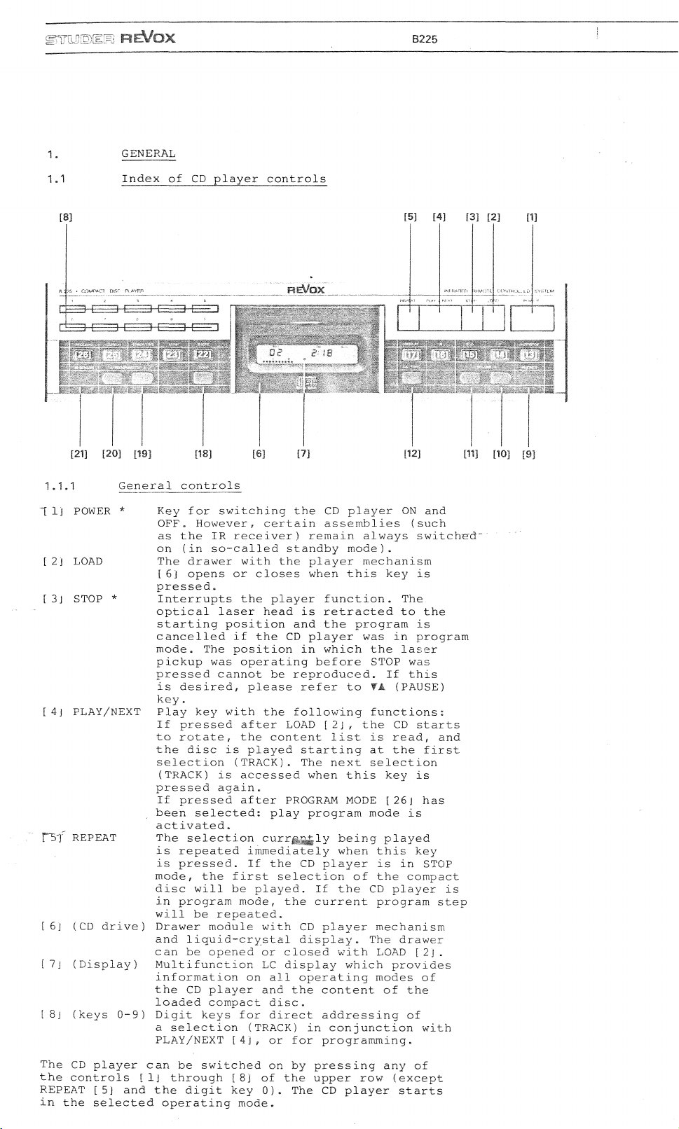
1.
1.1
1.1.1
1 Ij POWER *
[
2 j
LOAD
[
3 J
STOP *
[
4 J
PLAY/NEXT
H5"f REPEAT
[6j (CD drive)
[7j (Display)
[8j (keys 0-9)
GENERAL
Index of CD player controls
General controls
Key for switching the CD player ON and
OFF.
However, certain assemblies (such
as the IR receiver) remain always switched"
on (in so-called standby
The drawer with the player mechanism
[6j opens or closes when this key is
pressed.
Interrupts the player function. The
optical laser head is retracted to the
starting position and the program is
cancelled if the CD player was in program
mode.
The position in which the laser
pickup was operating before STOP was
pressed cannot be reproduced. If this
is desired, please refer to tJL (PAUSE)
key.
Play key with the following functions;
If pressed after LOAD [2j, the CD starts
to rotate, the content list is read, and
the disc is played starting at the first
selection
(TRACK) is accessed when this key is
pressed again.
If pressed after PROGRAM MODE [26 J has
been selected: play program mode is
activated.
The selection currf.r^ly being played
is repeated immediately when this key
is pressed. If the CD player is in STOP
mode,
disc will be played. If the CD player is
in program mode, the current program step
will be repeated.
Drawer module with CD player mechanism
and liquid-crystal display. The drawer
can be opened or closed with LOAD [2].
Multifunction LC display 'which provides
information on all operating modes of
the CD player and the content of the
loaded compact disc.
Digit keys for direct addressing of
a selection (TRACK) in conjunction with
PLAY/NEXT [4j, or for programming.
(TRACK).
the first selection of the compact
The next selection
mode).
The CD player can be switched on by pressing any of
the controls [ Ij through [8j of the upper row (except
REPEAT [5j and the digit key 0). The CD player starts
in the selected operating mode.
Page 4
mruim
REVOX
B225
1.1.2
The controls
roughly divided into
for supplementary player functions,
controls.
A Controls
[9] PHONES
[10] VOLUME
[11j VOLUME
[12]
CAL
13] AUTOSTOP
[ 14j
Key •
[ 15 J
VA
[16]
« key
[17] DISPLAY
Special controls
in the
+
-
TONE
*
(pause ) *
lower front-panel section
two
for
Headphones jaGk socket
200
Increases
and
Decreases
and
This calibration button connects
1000
outputs
of a connected tape deck
accurately adjusted.
CAL TONE corresponds
output level. This maximum level
is system-dependent
be exceeded even
pulses.
Interrupts
at
or program step.
is automatically positioned
the beginning
The next selection
immediately when PAUSE
pressed. Upon conclusion
selection,
again
Repositions
location toward
Interrupts
at
Repositions
location toward
Switches over
The time elapsed since
of
in normal PLAY mode.
play time from
current selection
by pressing this
function groups: controls
supplementary player functions
to 600
the
the
Hz
the end of the
any
the
ohms.
the
level
level
calibration tone
so
to
time.
current selection
headphones level
of the
the
headphones level
of the
that
the
of the
the CD
PAUSE mode.
the
the
the
the
can be
and
programming
for
headphones
VARIABLE OUTPUT.
VARIABLE OUTPUT
the
by
playing sequence
current selection
The
is
player switches
pickup from
the end.
playing sequence
pickup from
the
display mode.
the
start
can be
key.
to the
recording level
can be
The 1000 Hz
to the
and
short peak
laser pickup
next selection.
started
start.
The
maximum
will
not
at
TA [15] is
of
this
any
any
the
start
is
displayed
total
to the
displayed
a
These functions
PROGRAMMING keys
18] LOOP
19]
[20]
[21]
[ 22] STORE
[ 23] MARK
[24] TRACK/TIME
+
-
IR
*
SENSOR
can
also
be
programmed.
Command key for repeating the CD
or the proqr^4«until STOP [3j is
pressed.
Forward "paging" in program mode.
Particularly useful for modifying
an existing program.
Same function as [19] but backward
paging.
Infrared receiver window
Memory load key to be pressed after
each program step entry. The next
program step is subsequently
displayed so that the corresponding
entries can be made.
Allows a start and a stop mark
to be set in programming mode while
a selection is being played. Any
CD location can thus be programmed.
Switches the display in programming
mode from selection (track) input
to time input (minutes and
seconds).
Page 5
mWU\n)MPd
R^OX
B225
[25j CURSOR
[26 J
PROGRAM
Any position on the display can
be edited by approaching it with the
cursor.
TIME mode, the cursor must be
advanced with this key in order to
enter the seconds after the minutes.
Sets the program entry mode. If
PLAY/NEXT [4J is pressed after
the program entries have been
completed, the CD player starts in
PROGRAM mode,
If the CD player is to be started
in normal mode after the program
entries have been completed, press
the PROGRAM key
PLAY/NEXT [4].
NOTE; if the display is in
[ 26 J
again before
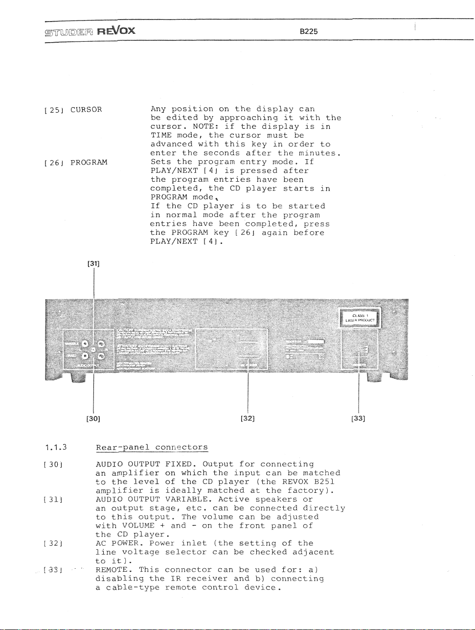
1.1.3 Rear-panel connectors
[30] AUDIO OUTPUT FIXED. Output for connecting
[31] AUDIO OUTPUT VARIABLE. Active speakers or
[32] AC POWER. Power inlet (the setting of the
..[33J
• "
an amplifier on which the input can be matched
to the level of the CD player (the REVOX B251
amplifier is ideally matched at the
an output stagef etc. can be connected directly
to this output. The volume can be adjusted
with VOLUME + and - on the front panel of
the CD player.
line voltage selector can be checked adjacent
to it ) .
REMOTE. This connector can be used for: a)
disabling the IR receiver and b) connecting
a cable-type remote control device.
factory).
Page 6
B^OX
B225
2 . REMOVAL OF ASSEMBLIES
Important:
Disconnect the CD player from the AC supply before
removing any parts of the housing.. For certain work
it is necessary to open or close the drawer module.
This can be done manually without damaging the unit.
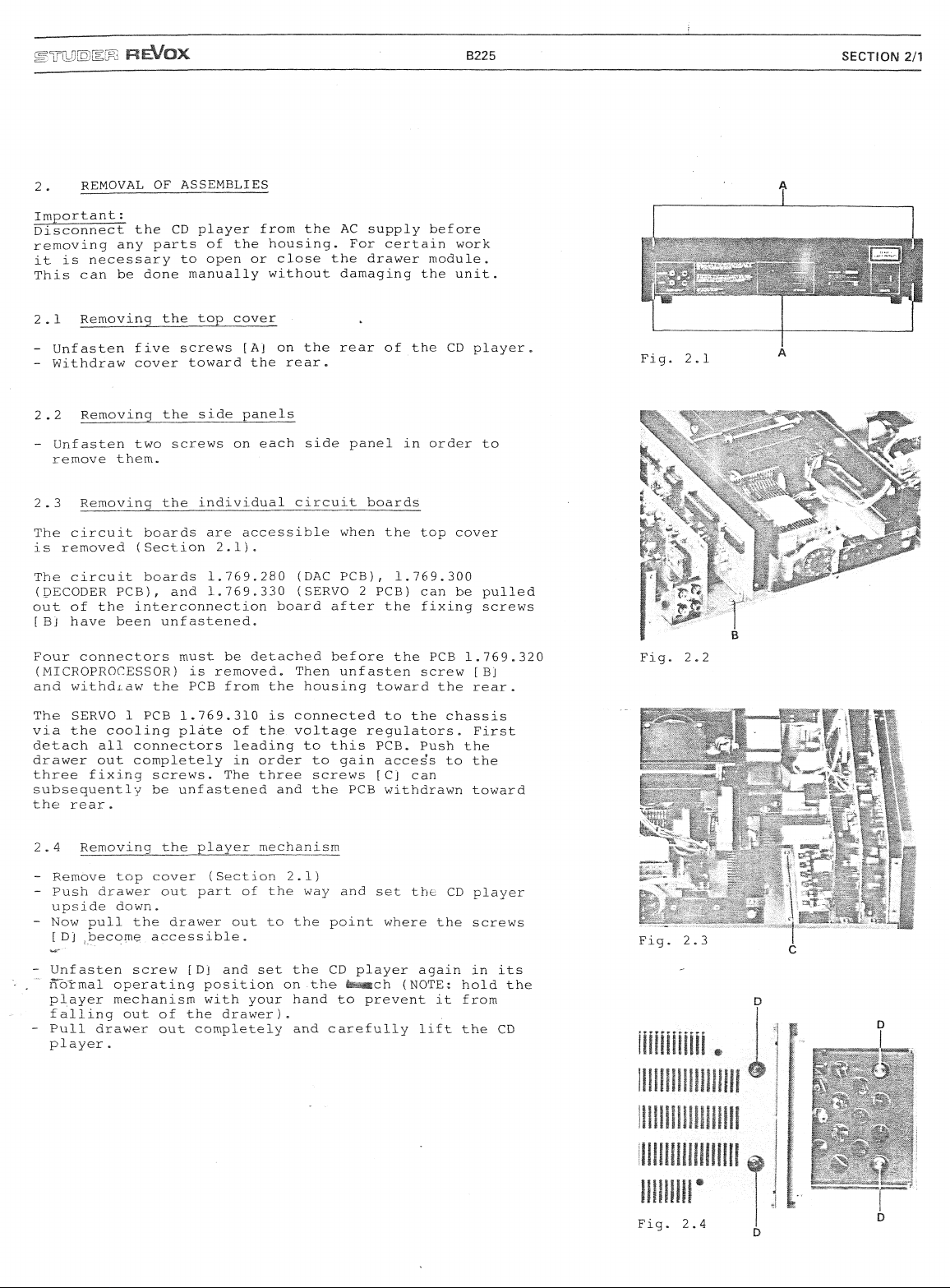
2.1 Removing the top cover
- Unfasten five screws [Aj on the rear of the CD player.
- Withdraw cover toward the rear.
2.2 Removing the side panels
- Unfasten two screws on each side panel in order to
remove them.
2
. 3
Removing the individual circuit boards
SECTION 2/1
The circuit boards are accessible when the top cover
is removed (Section 2.1).
The circuit boards 1.769.280 (DAC PCB), 1.769.300
(DECODER PCB), and 1.769.330 (SERVO 2 PCB) can be pulled
out of the interconnection board after the fixing screws
[ B] have been unfastened.
Four connectors must be detached before the PCB 1.769.320
(MICROPROCESSOR) is removed. Then unfasten screw [Bj
and withdraw the PCB from the housing toward the rear.
The SERVO 1 PCB 1.769.310 is connected to the chassis
via the cooling plate of the voltage regulators. First
detach all connectors leading to this PCB. Push the
drawer out completely in order to gain access to the
three fixing screws. The three screws [C] can
subsequently be unfastened and the PCB withdrawn toward
the rear
2
. 4
.
Removing the player mechanism.
- Remove top cover (Section 2.1)
- Push drawer out part of the way and set the CD player
upside down.
- Now pull the drawer out to the point where the screws
[ Dj ^become accessible.
- Unfasten screw [Dj and set the CD player again in its
- . ~ normal operating position on the
fc--^ch
(NOTE; hold the
player mechanism with your hand to prevent it from
falling out of the
drawer).
- Pull drawer out completely and carefully lift the CD
player.
Page 7
'umrnm ¥%EMOK
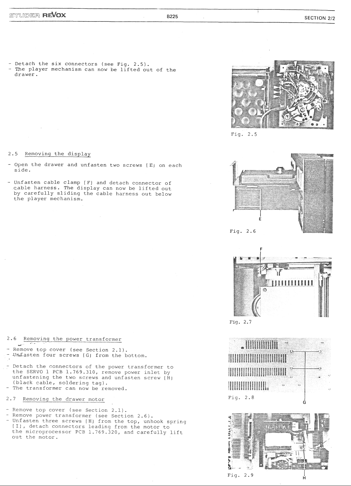
Detach the six connectors (see Fig. 2.5).
The player mechanism can now be lifted out of the
drawer»
2.5 Removing the display
B225
SECTION 2/2
- Open the drawer and unfasten two screws [ Ej
on each
side.
- Unfasten cable clamp [F] and detach connector of
cable harness. The display can now be lifted out
by carefully sliding the cable harness out below
the player mechanism.
2 •6
Removing the power transformer
- Remove top cover (see Section 2.1).
•
- JJniiasten four screws [Gj from the bottom.
- Detach the connectors of the power transformer to
the SERVO 1 PCB 1.769.310, remove power inlet by
unfastening the two screws and unfasten screw [Hj
(black cable, soldering tag).
- The transformer can now be removed.
2.7 Removing the drawer motor
- Remove top cover (see Section 2.1).
- Remove power transformer (see Section 2.6).
- Unfasten three screws [Hj from the top, unhook spring
[I],
detach connectors leading from the motor to
the microprocessor PCB 1.769.320, and carefully lift
out the motor.
Page 8
UJPEMKi KEl/OX
• .
B226
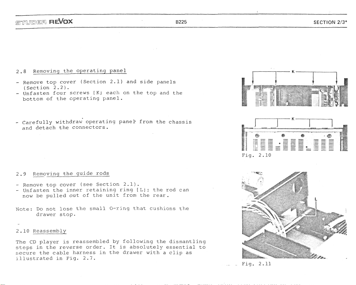
2.8 Removing the operating panel
- Remove top cover (Section 2.1) and side panels
(Section 2.2).
- Unfasten four screws [Kj each on the top and the
bottom of the operating panel.
Carefully withdraw operating panel' from the chassis
and detach the connectors.
2 -9
Removing the guide rods
- Remove top cover (see Section 2.1).
- Unfasten the inner retaining ring [Lj; the rod can
now be pulled out of the unit from the rear.
Note:
Do not lose the small O-ring that cushions the
drawer stop-
2.10 Reassembly
The CD player is reassembled by following the dismantling
steps in the reverse order. It is absolutely essential to
secure the cable harness in the drawer with a clip as
illustrated in Fig. 2.7.
Page 9
R^OX
3. CIRCUIT DESCRIPTIONS
B225
SECTION 3/1
3.1 SERVO 1 PCB
The following circuits are implemented on the SERVO 1
PCB;
- Stabilization of the supply voltages
- Drawer position detector
- Focus control loop
- Disc motor control loop
3.1.1 Stabilization of the supply voltages
All supply voltages are stabilized by voltage controllers
(IC 4 to IC 9,
The +5V supply (+5 V STBY) is always available. It
supplies the microprocessor system and the IR receiver
even when the CD player is switched off
The remaining supply voltages are switched on or off
by the microprocessor with the PS-OFF signal. When
the CD player is switched off, PS-OFF becomes "H" (+5 V)
and transistors Q9 and Q10 become conductive
(staturated),
to drop to a residual voltage of 1.3 V. The -7 V supply
is switched off through the circuit R38,
the -12 V supply via R52, R54, and Qll; and the -17 V
supply via R51,
supply voltages from becoming negative. The voltage
is doubled through diodes D15, D16, D17 and capacitors
C29,
C30# and taken to the voltage controller IC9 for
the -17 V supply. D18 protects the controller from
an excessive direct-axis component of the voltage.
1.769.310
LM317/LM337).
(standby).
causing the +5 V and +12 V supply voltages
R39? and Q8;
R53f and Q12. This prevents the positive
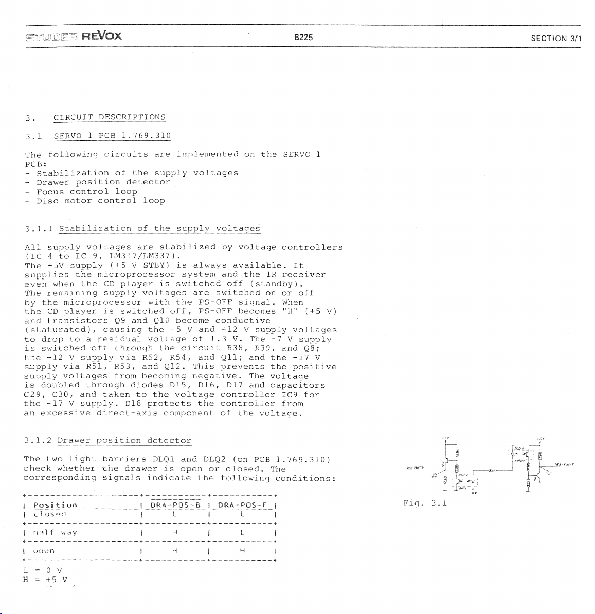
3.1.2 Drawer position detector
The two light barriers DLQ1 and DLQ2 (on PCB
1.769.310)
check whether the drawer is open or closed. The
corresponding signals indicate the following conditions:
Page 10

R^OX
B225
3.1.3 Focus control loop
The lens can be moved vertically and is designed similar
to the mechanical system of a speaker. The lens is
controlled magnetically. The coil is stationary and
the magnet moves. The focus error signal FOC-ERR is
first amplified (lead amplifier IC2a, R3, R12, R16,
R17,
C3, C4) and subsequently taken to the controlling
amplifier
R30,
lens
("lag"
amplifier Rl, R2, R5, Rll, R15, R29,
C2, C12, IC2b, Q6, Q7 and the impedance of the
coil).
In STOP mode, the control loop is interrupted
via Ql by the signal FOC-0 {= H) which means that no
unnecessary power is consumed by the output-amplifier
(Q6 and Ql).
SECTION 3/2
The start-up circuit (IC1, R6, R7 ) adjusts the focussing
to the reflective layer of the compact disc. The signals
FC-1 and FC-2 are alternatingiy switched to "H", causing
the lens to move alternatingiy up or down. Once the
correct focus has been found, the signal FOC-NEG briefly
drops to "L". The microprocessor then enables the focus
control loop
(FOC-0,
FC-1, and FC-2 -
"L"
)..
Up to 12,000
tracks per second are skipped in fast search mode.
Because the focussing lens readjusts for each track, a
whistling sound of approximately 12 kHz would develop as
is the case with a speaker. This whistling sound is
eliminated by R60, R61, C31, Q13 in the control loop.
This filter is only active in search mode.
3.1.4 Disc motor control loop
The data from the compact disc must be supplied as
steadily as possible to the digital signal processing
circuit.
depends on the position of the laser pick-up (constant
peripheral speed between 1.2 and 1.4 m/s).
If the laser pick-up reads in the middle of the CD,
the^speed is-much higher than near the edge. The speed
correction signal MCES is generated in the error
correction Ic"(SAA 7020 on PCB
The signal MCES is switched off or on via the signal
FOC-0 (R15, R16, IC3b on PCB
is first filtered via a 2nd order low pass (R22, R23,
R25r R26, R28, C10, Cll,
is formed by C9,R19, R21, R24, and R28, the
by IC3a, C6, C7 , R8 , Q2, and Q3.
As soon as the focal point has been found, the signal
FOC-0 changes to "LOW1' and the signal MCES is enabled.
A negative pulse via C5 is simultaneously triggered on
IC3a,
to rapidly accelerate the compact disc. The speed is
subsequently controlled by the MCES signal.
The speed with which these data (bits) arrive
1.769.300).
1.769.330).
IC3b).
pin 3, thereby fully driving transistor Q3 in order
The "lead network"
The signal
,r
lag network"
Page 11

WmrMM R^I/OX •
B225
•
SECTION
3/3
3.2 Microprocessor PCB
The microprocessor system and the drawer control are
implemented on the microprocessor PCB 1.769=320.
3.2.1 Microprocessor system
The master microprocessor (M-jiP, IC2 ) scans the keyboard
(POO to PG5, P10 to P14). The microprocessor system is
reset when the LOAD key is pressed. To enable
differentiation between a power failure and a LOAD
command, P15 of the master processor is also pulled to
"LfI in conjunction with a LOAD command. Capacitor C12
latches this condition until P15 is read. This
unconventional circuit arrangement offers the advantage
that a RESET command can be initiated at any time by
pressing the LOAD key in the event that the system
becomes blocked for any reason.
The commands from the IR receiver or the REMOTE socket
are read through the interrupt input of the master
processor . When a command arrives from the IR remote
control,
approximately one second, causing the LED in the IR
receiver window to turn on (command acknowledgment).
The signals
with drawer position information.
The signals CLK, DATA,
two LCD drivers PCE 2111 (on PCB
The gain of the headphones amplifier and the
VARIABLE OUTPUT is controlled by the signals CLK, DATA,
and DLEN-3 (on PCB
The slave microprocessor (S-]iP, IC4 ) processes the
subcode (supplementary information on the compact disk
such as track, time,
originate from PCB
Q-SYNC, SWCLK, Q-DATA, and
The-signals RC-0 and RC-0 switch the radial-control
loop on or off. When the radial control loop is switched
off (RC-0 = L), the laser pick-up can be repositioned
with the signals RCl, RC2, CUR-SUM, and CUR-DIR.
The track signal (TRK) is read through the interrupt
input of the slave processor. This signal changes to
"L"
direction in which the laser pick-up moves is reported
to the slave processor by the signal Tl. This signal
also changes to "L" as soon as the laser pick-up passes
over a track. It is also used in search mode for counting
the tracks. Because the counting speed of the
microprocessor is not high enough, only every other track
is counted in fast search mode (division by 2,
Any program entered through the keyboard Is stored
serially ,in.IC5 (serial RAM).
Both microprocessors are initialized by IC1 (reset chip
TL
7705).
via pin 7. A reset is also ' initialwai via Rl/ R8, and C8
when the LOAD key is pressed.
Commands from a cable-type remote control can be read
through the REMOTE socket (pin 2 and pin 3). These
commands are electrically isolated through the
optocoupier IC 12a. These signals are converted to
TTL signals by the comparator circuit (IC9a, R44, R45,
R48,
the infrared receiver, the voltage at pin 4 must be
higher than on pin 2 by +5 V. The +5 V STBY of the REMOTE
socket can be used for this purpose (interconnect pins 1
and 2, pins 4 and 5). The IR signal is thus short-
circuited via
the IR-REC signal is switched to "LOW" for
BRA^TOS3!
as soon as the laser pick-up passes over a track. The
The +5 V STBY supply is supervised by ICl
and R60). In order to disable the commands from
DLQ2,
1.769.320
and DRA-POS-F supply the processor
DLEN-1,
1.769.280).
etc.).
1.769.300
R41, R42, R43, R62, and IC9b.
and DLEN-2 control the
1.769.250).
The required signals
(IC13, SAA 7010, signals
P-BIT).
IC6b).
Page 12

57,
B225
and
C13,
r^;-:;:^,-
3.2.2 Drawer motor control
The drawer motor amplifier (IClOa, R52,53,56,
R58,
C14, Q8 and Q9) is controlled through the shift
register IC3 (pins 4 and 5). If the drawer movement
is blocked during the opening or closing operation,
the motor current rises and hence the voltage across
R64.
Signal Tl of the master processor consequently
changes'to "L" (circuit R40,54,55,59,63,
and
IClOb).
the direction of the drawer movement.
n^ox
Q6,^Q7,
In response the master processor reverses
SECTION 3/4
3.3
The SERVO 2 PCB
radial control and the IR receiver.
3.3.1 Radial control
A moving arm allows the laser pick-up to follow the
track horizontally. This arm basically functions like
a moving coil instrument.
The radial-control circuit can be subdivided into four
blocks:
- Radial control circuit
- AGC circuit
- Offset control circuit
- Track detection circuit
3.-3.2
The value of the radial-error signal can be computed
as follows^ RE= kd (II +12+13 +14) - k (II + 12).
The value of k is determined by the AGC circuit, and
d by the offset control circuit.
RAD-ERR2 =11+12
RAD-ERR1 =13+14
The signals RAD-ERR1 and RAD-ERR2 are summed via the
circuit IC9b, R58/59/61/62/63 and Q6. The sum flows as a
current through R63 and Q6. The error signal RAD-ERR 2 is
converted via R55 and R57 to a current that flows through
R54 and transistor E of IC8. The factor k is formed by
transistors A and B as well as C and D
formed by Q5 and transistor F
The signal RAD-ERR 2 x k (=k [II + 12]) on pin 10 of IC9c
appears on pin 9 of IC9c; the signal [RAD-ERR1 +
RAD-ERR2J kd (= kd [11 + 12 + 13 + 14j) appears on pin 10
of IC9c. The difference signal (RE), developed in IC9c,
appears on Pin 8 (RE = kd [II + 12 + 13 + 14 j - K[I1 +
K2j ). The "lag" network of the radial control is
implemented by R66, R67, R68, C15, and IC9d, the "lead"
network by R69, R7
IC5 through the protective diodes D5 and D6. The signal
is^taken through switch B (IC5) to pin 2 of IC2 which
together with Q2, Q3; R6, R7", R8, RT1, and C5 constitutes
the_output stage for the radial-control signal RAD-MOT+/
-RAD-MOT-.
disabled (Signal
forward and reverse mode. The laser pick-up can be
positioned during this phase with the signals RC-1, RC-2,
CUR-DIR, and CUR-SUM.
SERVO-2 PCB
Radial-control circuit
RT1 protects the
1.769.330
1.769.330
0,
RC-o).
contains the circuits for
and C16. The signal is conducted to
coil;-
This occurs in search, pause,
(IC8).
(IC8),
ThJBMwontrol can be
factor d is
Page 13

KEI/OX
B225
3.3.3 Automatic gain control (AGC) circuit
The bandwidth of the radial-control circuit is stabilized
by this circuit. A 650 Hz sine-wave signal is generated
in the circuit IClOc, IClld, C22,
R86,
R87? R90, and R91. As the gain increases or
C23# C24, C25,
R85
r
decreases the phase relation of the supplied signal
becomes also larger or smaller with respect to the
returning signal* The two signals are compared in the
phase detector (ICll) and a new signal is developed.
The latter is proportional to the phage and also to the
gain.
This signal controls the factor k. The gain is laid,
out for a" phase shift between the signals -of -.135° The
650 Hz.sine-wave signal is therefore fed into the control
loop at pin 13 of IC9d through a 45° phase shifter (R84,
C21).
The phase shift is 90° at the input of the phase
detector. The 650 Hz sine-wave signal is eliminated from
the control circuit through a bandpass (IClOd,
R83,
C19, C20) and converted in IClla to a square-wave
signal.
This square-wave signal is input to the phase
R82
r
comparator (ICllc, pin 8). The phase reference is
supplied by pin 9 of ICllc.
3.3.4 Offset control circuit
The asymmetry of the reflected laser beam is corrected
by this circuit to ensure that the laser beam is kept
exactly on the center of the track. The difference
between minimum and maximum reflection is the greatest
(presence of pit = minimum reflection, between pits
= maximum reflection) when the laser beam follows exactly
the center of the track.
SECTION 3/5
Through the 650 Hz sine-wave signal the moving arm
oscillates with an amplitude of 0.05 jim.
If the laser beam is on the track center, all half-waves
of the filtered out signal are folded to the same
(positive) side. If the laser beam is to the right of the
track center, the signal is in~phase with the 650 Hz
oscillations of the moving arm, or antiphase if the beam
is on the left of the track center.
The voltage across R63 is proportional to the reflected
light intensity
through IC6a,
(11 + 12 + I3 + I4).
R30f R31r and
The voltage is amplified
R64# and the 650 Hz component
is filtered out in a bandpass (R32, R33, R34, R35, R37,
Cll,
C12, and
IC7b).
The filtered signal is inverted
through lC7ar R36, and R38. The former and the
noninverted signal are taken to switch C of IC5. The
output of this switch (IC5, pin 4) is integrated through
IC7d and C.30 and determines the factor d (Q5 and
transistor' F of IC8). The status of switch C (IC5)
is controlled by the 650 Hz signal in the control loop
. -vara-the bandpass
R42f R43r R44 , R45, C13, C14 , D4,
" and IC7c.
Page 14

WT^ZJ'jLTi R^OX
B225
3 . 3.5 Track detection circuit
The tracks which are skimmed over by the laser pick-up
are read through the interrupt input of the slave
processor
(TRK-SIG).
This signal is generated from the
signal available at IC6, pin 1 (proportional to
[
I1 +
I2
is
+ I3 + I4J
,!L,!
when no error location is detected on the CD.
),
the DO and the HFL signal. The signal DO
The HFL signal is "H" when the HF signal is large enough.
The TRK signal is only "L" when the HE signal is too
small.
location is detected on the CD
For each skipped track, HFL is "L" if no error
(DO="L").
The radial-error
signal RE (IC9c, pin 8) informs whether the laser scanner
is positioned to the left or the right of the track. The
signal required for this purpose (RAD-POS) is generated
via IC3c, R12, R19, and R20 from the radial-error signal.
3.4 Preamplifier and laser PCB 1.769.100.35
This board comprises the following circuits:
- Laser control
- Signals for focus and radial control
- HF signal amplifier
SECTION 3/8
3.4.1 Laser control
The laser diode is supplied via Q4. The intensity of
the laser light can be checked through the "monitor
photo diode" and adjusted with the trimmer potentiometer
R8CT.
The signal LAS-OFF (from PCB
1.769.310
/ IC1) switches
the laser on or off. If the intensity of the laser
becomes too small, the current flowing through the
monitor photodiode decreases correspondingly. The voltage
across R84 also drops. The output of.opamp IC3a
consequently becomes more positive and Q4 more
conductive. The intensity of the laser is adjusted by
discharging some of the current through the monitor
photodiode via R80 and R81.
3.4.2 Focus and radial-control signals
The following signals are generated by this circuit;
- FOC-ERR
- RAD-ERR1
- RAD-ERR2
The currents of the four photodiodes (Al to A4) are
amplified in IC1. The corresponding error signals are
developed by the subsequent network. The focus error
signal is proportional to (11+14) -
(12+13).
13 + 14
constitutes the•RAD-ERRl signal, II + 12 the RAD-ERR2
signal.
The gain of the focus control loop can be
-^djiis/ted with R58, the balance with R41 (not included in
'all
versions).
" '3-4.3 HF signal amplifier
The circuit comprising transistors Ql through Ql constitutes the signal amplifier with bandpass characteristic.
Low-frequency (e.g. control signals of the servos)
and high-frequency disturbance signals are consequently
filtered out.
3.5 Decoder PCB
1.769.300
The decoder PCB contains the following circuits:
- Digital signal processing
- Digital sine-wave generator
- HF£ and DO detector
Page 15

mnruiDjiMM HEMOX B225 SECTION 3/7
3.5.1 Digital signal processing
The HF signal is converted in IC13 (SAA 7010} into
diqital siqnals and split into audio and information
data (subcode, for the slave
signal is also regenerated in JC13. The audio data
are brought into the correct time slot pattern. Corrupted
audio data are not recognized in 1C12 and corrected
if necessary. Should the errors be incorrigible, the
missing sample values are replaced in. IC10 (SAA 7000)
through interpolation. Should this also be infeasible,
the HF signal is slowly muted (soft
of the CD motor is controlled by the signal MCES (IC1,
pin
4 )
.
3.5.2 Digital sine-wave generator
The PROM (IC4) contains a value table for the sine-wave
signal which represents the maximum possible level
of a CD.
The circuit consists of IC5 through IC9 with IC5 and
IC6 supplying the addresses for the PROM. Parallel/serial
data conversion is performed in IC3. The change-over
between audio data from the CD and the 1 kHz sine-wave
signal is controlled by IC1.
3•5•3
HFL and DO detector
The HF signal is fed into the inverting differential
amplifier Ql and Q2 through C6 and R2. The output signals
are DC-decoupled via C8 and C9 respectively and tied
to DC ground via D2 and D3. D4 and D5 or D6 and D7
respectively constitute a full-wave rectifier each
through which the capacitors C10 or Cll are charged.
With a normal HF signal the DO signal is "LSi and the
HFL signal is "H". If the HF signal drops to approximately 70% of the normal value, the HFL signal also
changes to
!,Lt!
.
Only when the HF signal drops to
approximately 10% of - the normal value does the DO signal
change to "H".
To prevent the output signals of IC11 from being
influenced too strongly by minor contaminations (e.g.
fingerprints) on the CD, transistor Q3 has been added to
the output. When the RF level is at nominal value, pin 7
of IC11 is
"Hl! .
Q3 becomes conductive and the circuit
with Cll receives a smaller time constant. With level
fluctuations caused by minor contaminations, the levels
of the two input capacitors fluctuate in parallel, but
neither the DO nor the HFL signal are affected.
processor).
muting).
The CLOCK
The speed
3.6 DAC PCS
Tfee"
following'circuits are implemented on this PCB:
1.769.280
.
- Digital filtering (oversampling) and digital/analog
- •conversion
- Level adjustment and headphones" aTifffiifier
3.6.1 Digital filtering (oversampling) and D/A conversion
IC1 (SAA 7030) contains two identical filters for both
channels. These filters feature 3 sections:
~ Oversampling section
- Transversal digital filter
- Noise shaper
After each scanning cycle, the new sample values are
inserted by interpolation into the 16-bit information
arriving from the decoder. The scanning rate thus becomes
4 times greater (4 x 44.1 kHz = 176.4 kHz). The spectral
lines above 20 kHz up to 176.4 kHz - 20 kHz are filtered
out by the transversal filter. The sample values are
truncated to 14
bits.
The noise shaper subsequently
delays the truncation error by the scan duration and
negatively added to the next sample value. The
guantisizing noise caused by truncation is thereby
largely shifted toward the frequency range above 20 kHz.
The digital signal is converted in IC101 or IC201
(TDA 1540) to an analog signal. In order to filter out
the residual frequency component at n (176.4 kHz
+; 20 kHz), a low pass of the third order (Bessel filter)
has been added to the converter output.
Page 16

r'r:;T*5^
The preemphasis is corrected with the circuit illustratec
in Fig. 3.13. The subcode on the CD specifies whether
the selection was recorded with or without preemphasis.
The characteristic of the corresponding filter can
be adjusted with the PREEM signal.
3.6.2 Level adjustment and headphones amplifier
The volume is controlled by a DUAL D/A converter
(AD7528).
corresponding input (IC103a, pin 2 = left-hand channel
/ IC 203bf pin 6 = right-hand
feedback resistances of both opamps remain unchanged
which means that the level can only be attenuated with
this circuit. The dual D/A converter is controlled by a
CMOS shift register through the signals DLEN-3, DATA, and
CLK. The circuit illustrated in Fig. 3.14 constitutes the
output amplifier for the headphones socket and also
the VARIABLE OUTPUT* The signal is also attenuated for
this purpose through a voltage divider so that the signal
is the same (2 V RMS) at both outputs (FIXED and
VARIABLE).
to prevent power-on switching clicks. When power is
applied., the relay is selected by the
KILL signal (which rises to +5 V after approximately
1 to 2
through-connected when the supply voltages are stable.
R^QX
It serves as an attenuator before the
channel).
The signal is taken through relay Kl in order
seconds).
As a result, the outputs are only
The negative-
B225
SECTION 3/8*
Page 17

REI/OX
4.
TEST POINTS, ADJUSTMENTS ON
4 m i
Test points on B225
B2 2 5
4.1.1 Test points on SERVO 1 PCB 1.769.310
B225
SECTION 4/1
Page 18

'lDj[j
If no CO is mounted when PLAY is selected* the signals on TP26
an
CJ
2 7 become ^l?V in four intervals of approximately one second
each • "
R^OX
B225
SECTION 4/2
(*) In PLAY- mode* the signal pattern of these test points depends
on the wobble of the mounted compact disc*
Page 19

w^rumi
4.1.2 Test points on SERVO 2 PCB 1.769.330
R^OX
B225
SECTION 4/3
Page 20

h FtEMOX
B225
SECTION
4/4
when signals
•4.3V occur
4.13 Test points on MICmPRGCESSQR PCB 1.769.320,
are
on
received froni
TP52«
the IR-
remote control t pulses
of
Page 21

R^OX
6225
SECTION
4/5
Page 22

^T'^\£:WM REl/OX
B225
'
SECTION 4/6
Test with reference CD part No. 46241
Black dots
are
located
on
track 17
of
the disc surface* The
following should be measured v^hen this track is played:
Page 23

WUMEM
FIEMQX
B225
SECTION
4/7
Page 24

L
^£=.1^
FIEMQK
B225
SECTION 4/8
4.1.5 Test points on DAC PCB
1,769.280
The internal calibration must be switched on for the
following measurements;
Page 25

=
c^.
4 m2 Adjustments on CD player B225
Note:
Cleanliness
and ensures that
can enter into the
KEI/OX
in
the work area
no
contaminants
CD
mechanism.
is of
or
B225
outmost importance
metal particles
SECTION 4/9
If any work
it
is
(refer
Before putting the
on
essential
to
last page
printed circuit boards
to
observe the ESE recommendations
of
contents).
CD
player into operation ensure
is
necessary,
that the transport screws have been unfastened.
The
CD
bearings which should not
player mechanism
If the drawer must
to perform certain measurements
•rear light barrier must
responds
disc must
as if
be
the drawer were closed) and the compact
secured with a removed adhesive magnet.
The optical system
is
equipped with self-lubricating
be
lubricated.
be
open and a disc mounted
be
of
the laser can
or
adjustments,
interrupted (the detector
be
in
order
the
cleaned with
an air brush.
Coil Ll on the decoder PCB
aligned by IC13 (SAA7010) and consequently requires
no adjustment*
4.2.1 Aids
-
DC
voltmeter
1.769.300
is automatically
- Cathode ray oscilloscope
- Reference CD, frequency response, part No. 46240
- Reference CD, drop
- Mirror
No.
- Set
CD
for adjusting the optical system, part
46242
of
service PCBs and cables, part No. 46230
outs,
part No. 46241
- ESE work location kit, part No. 46200
4.2.2 Aligning
player mechanism, general
- Remove top cover.
- Connect
CD
player
to AC
supply and open the drawer
by pressing the LOAD key.
- Cover rear light barrier.
- Mount reference disc 5 (part No. 46241) and secure
it with a removed adhesive magnet.
- Selection
work.
LOOP.-command
1 of
It
is, therefore^ advantageous
the
CD is to be
in
programming mode.
played for all alignment
to
enter
the
"4T2". 3 Adjusting the laser current
- Switch
and reinsert
- Connect
- Adjust the voltage
CD
player off, remove SERVO 2 PCB
it
DC
via the service PCB (part No.
voltmeter
to
to
500
R63
mV
on
SERVO 2 PCB.
+50
1.769.330
mV
with the trimmer
46230).
potentiometer RS0 (on player mechanism 1.769.100.35).
Adjustments should only
be
made
if
the measured voltage
is outside the specified tolerance range.
CAUTION:
Voltages above 550
mV
shorten the life
of
the laser
pick-up.
- Switch
4.2.4 Adjusting the balance (if trimmer
CD
player off and reinstall SERVO 2 PCB.
is
present)
- Set potentiometer R41 (on player mechanism
1.769.100.35)
to
its center position.
Page 26

REMGX
B225
4.2.5 Adjusting the focus gain
-- Switch CD player off, remove SERVO 1 PCB 1.76 9.310
and reinsert it via the service PCB.
- Connect AF generator to the X input of an oscilloscope
and via an R-C-R element (according to Fig. 4.12)
to pin 6 of IC2 (on
1.769.310),
(f=600 Hz +5 Hz,
U=250 to 300 mV RMS).
- With trimmer potentiometer R58 (on player mechanism
PCB 1.769.100.35), align for minimum amplitude A
of the Lissajous figure.
SECTION 4/10
, 2 .
6 Checking the angle alignment
t
Place the mirror on the focussing unit and mount
the optical system alignment disc (secure with adhesive
magnet) .
Place the player mechanism below? a light source that
produces a linear, straight shadow.
Bring the-laser scanner arm to its center position
and rotate the CD player in such a way that the arm
stands parallel to the line below? the light source
(refer to Fig.
4.13).
When the reflection on the glass disc and in the
mirror is viewed as illustrated in Fig. 4.13. The
distance between the two lines should not exceed 2.5 mm.
Position the CD player in such a way that the shadow
forms a 90° angle to the scanner arm (see Fig.
4.14).
The distance between the two lines (reflections)
should not exceed 2.5 mm.
Page 27

^-yiLr^Ju
The angle alignment must be corrected if the deviation
is too large:
- Unfasten screw [A] until the support plate [ B]
be shifted.
- The support plate can now be shifted according to
Fig*
is correct.
- The angle alignment must be rechecked after the
foregoing adjustments have been made.
4.2.7 Adjusting the DC component of the focus signal
- Connect DC voltmeter to Rl (SERVO 1 PCB 1.76
The following adjustment is only necessary if the DC
deviation exceeds
is not possible.
- Adjust the axial set screw of the disc motor in such
a way that 0 V +_50 mV is measured.
- If the motor is replaced, perform the adjustments
according to 4.2.6 and 4.2*7*
4.3 Measuring the audio data
R^OX
4.5. Retighten the screw [A] when the position
+JL4 0
mV. Replace the motor if alignment
B225
can
9.310).
SECTION 4/11
4.3.1 Aids
-_ Reference CD, part No. 46240
- Automatic distortion meter (e.g. Tektronix AA 501;
the RESPONSE button must be in the RMS position for
all measurements)
- Measuring filter (for distortion measurement)
~ Frequency counter
- Oscilloscope
4.3.2 Harmonic distortion
- Measuring arrangement according to Fig. 4.16
- Adjust for maximum level with VOLUME + key
- Mount reference disc (part No.
4 for measuring the left-hand channel and track 8
for measuring the right-hand channel.
- The harmonic distortion should be less than 0.006%.
4.3.3 Output level
- Press CAL TONE button and adjust for maximum level
with VOLUME + key.
- The level of the FIXED and VARIABLE outputs should
be 2 V RMS +10%. The balance between channels should be
better than 0.2 dB.
4^,3 . 4 -Frequency response
- Adjust for maximum level with VOLUME + key.
"'-—The calibration tone (1 kHz) serves as the 0 dB
reference.
- Play tracks 4 and 8 (CD part No. 46240) and measure
the outputs FIXED and VARIABLE. The frequency response
shoul-d be within +0 to -X3.6 dB.
46240).
Play track
Page 28

?rr-S-£:JL\Fi FI&/OX B225 ! SECTION 4/12*
4.3.5 Cross talk
- Adjust for maximum level with VOLUME + key,
- Reference = CAL TONE 1000 Hz)
- Measure both outputs across a 30 kHz low-pass:
Play track 8 for measuring cross talk R -> L
Play track 4 for measuring cross talk L -> R
- The cross talk attenuation should be at least 90 dB.
4.3.6 Signal-to-noise ratio, linear
- Maximum volume, reference = CAL TONE 1000 Hz.
- Play track 18 and measure the outputs FIXED and
VARIABLE via a 30 kHz low-pass.
- The measured value should be higher than -96 dB,
4.3.7 Signal-to-noise ratio, weighted
- Maximum volume, reference = CAL TONE 1000 Hz.
- Play track 18 and measure the outputs FIXED and
VARIABLE via an A filter.
- The measured value should be higher than 100 dB,
4.3.8 Phase linearity
- Connect oscilloscope to one of the outputs.
- Play track 20 and visually assess the square-wave
signals at 100 Hz, 400 Hz, 1002 Hz, and 5512 Hz.
The curve should be shaped symmetrically (see
Fig.
4.17).
, .
4.4 Listening test with reference CD (part No. 4 6241)
The reference CD simulates the following errors for
checking the error correction system:
- Information gaps with a length of 400 to 900 pm (tracks
5 through 9)
- Black dots from 300 to 800 micrometers
(tracks 1*1 through track 17)
- Simulated fingerprint (tracks 18 and 19)
The simulated defects should not cause any drop-outs
(reproduction
can for example be caused by the following errors:
- IC13 (SAA 7010,
with PLL defect.
- HFL an DO detector defective.
gaps).
If drop-outs become audible, this
demodulator),
clock regeneration
Page 29

 Loading...