

Page 1
USER’S MANUAL
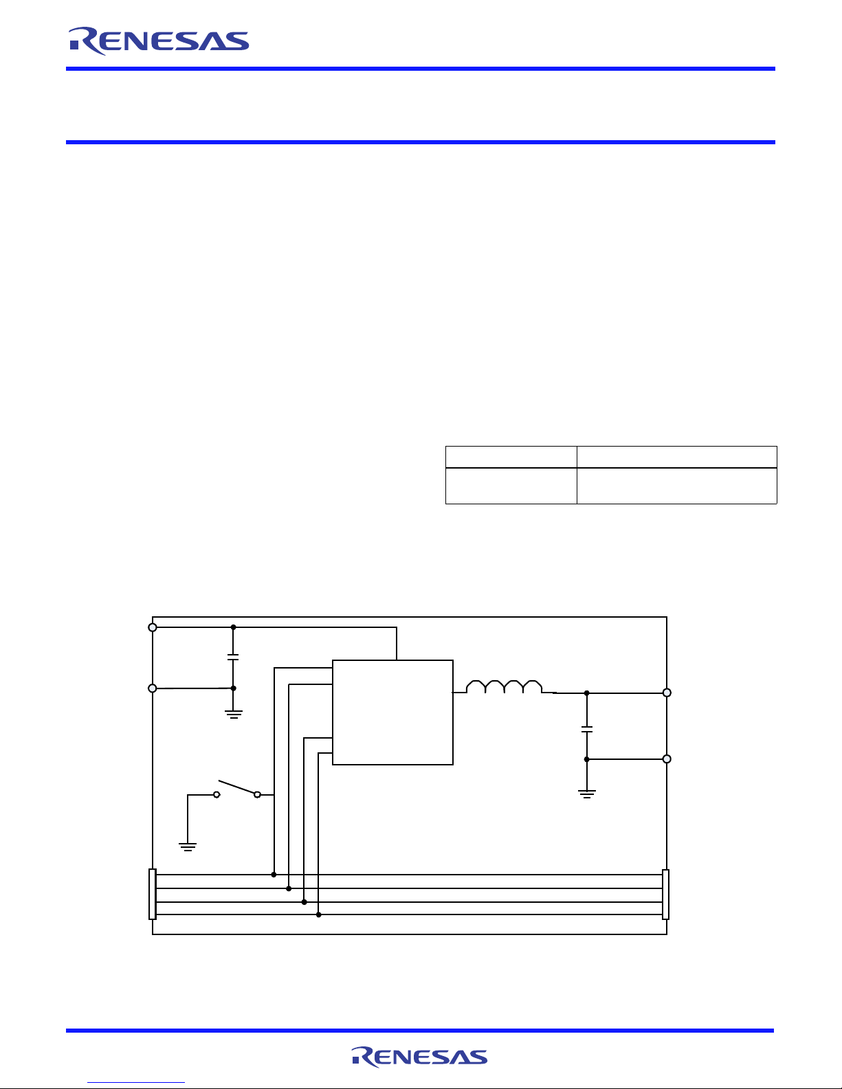
FIGURE 1. ZL2102DEMO1Z BLOCK DIAGRAM
ZL2102
DDC
SMBus
V
OUT
EN
SYNC
ENABLE
SW
1
ENABLE
SYNC
DDC
SMBus
ENABLE
SYNC
DDC
SMBus
V
IN
ZL2102DEMO1Z
Demonstration Board
Description
The ZL2102DEMO1Z is an innovative power conversion and
management IC that combines an integrated synchronous
step-down DC/DC converter with key power and fault
management functions in small package, resulting in a flexible
and integrated solution. The ZL2102DEMO1Z platform allows
quick evaluation of the highly configurable ZL2102DEMO1Z’s
performance and features in either stand-alone mode or via
the SMBus™ interface using Intersil’s PowerNavigator GUI
software.
Specifications
This board has been configured and optimized for the following
operating conditions:
•V
= 12V
IN
= 3.3V
•V
OUT
= 6A
•I
MAX
= 600kHz
•f
SW
• Peak efficiency: >85% at 50% load
• Output ripple: <0.5% at 6A
• Dynamic response: 3.5%
(3A to 5A and 5A to 3A steps, di/dt = 2.5A/μs)
• Board temperature: +25°C
AN1874
Rev 0.00
August 6, 2013
Key Board Features
•Small, compact design
•SMBus™ control interface
range of 7.5V to 14V
•V
IN
adjustable from 0.6 V to 3.6 V
•V
OUT
• Convenient power connection
• Onboard enable switch
• Power-good indicator
• Interconnectivity with other intersil demo boards
References
FN8440 “ZL2102” Data Sheet.
Ordering Information
PART NUMBER DESCRIPTION
ZL2102DEMO1Z ZL2102 Evaluation Kit, one channel
(EVB, USB Adapter, Cable, Software)
AN1874 Rev 0.00 Page 1 of 12
August 6, 2013
Page 2

ZL2102DEMO1Z
Functional Description
The ZL2102DEMO1Z Demo Board provides a simple platform to
demonstrate the features of the ZL2102. The ZL2102DEMO1Z
has a functionally optimized ZL2102 circuit layout that allows
efficient operation up to the maximum output current. Power and
load connections are provided through plug-in sockets.
Standalone operation is achieved using a combination of
pin-strap settings and stored settings. The pin-strap setting
details are described in the ZL2102 data sheet. The stored
settings are listed in “Default Configuration Settings” on page 11.
The ZL2102DEMO1Z Demonstration Board is shown in Figure 2
and Figure 3. The hardware enable function is controlled by a
toggle switch. The power-good (PG) LED indicates that V
regulating. The right angle headers at opposite ends of the board
are for connecting a USB to SMBus control board or for daisy
chaining of multiple Intersil evaluation boards.
Connecting multiple Intersil Zilker Lab boards allows the user to
setup many shared features such as clock synchronization,
controlled sequencing, phase spreading, and fault spreading
within Intersil’s Power Navigator software as part of a single
power project. The ZL2102DEMO1Z Circuit Schematic (Figure 9)
shows the schematic, bill of materials, and PCB layers for
reference. Figures 10 through 13 show performance data taken
using this hardware in its optimized configuration. The
configuration settings that the hardware ships with are shown on
Page 11.
OUT
is
Operating Range
By default, the ZL2102DEMO1Z is configured for the operating
conditions shown in “USB (PMBus) Operation”. The board can
also support a wider operating range, and modifying the
operating conditions will change the performance results.
The board VIN range is 7.5V to 14V. The board V
fixed at 3.3V by pin strap setting, but the programmable range is
0.54V to 3.6V (including margin high/low). The output voltage
can be changed by using the VOUT_COMMAND PMBus
command. The board I
operation at 6A, airflow across the board may be needed.
The switching frequency (f
command, but the f
FREQUENCY_SWITCH PMBus command (while the device is
disabled). The fSW range is 200kHz to 1MHz.
range is 0 to 6A. For continuous
OUT
) is set to 600kHz by PMBus
SW
setting can be changed by using the
SW
setting is
OUT
PCB Layout Notes
The ZL2102DEMO1Z PCB layout has been optimized for
electrical and thermal performance.
The following key features are:
• The large 5x5 via pattern under the ZL2102 is connected to a
large copper plane for effective thermal dissipation.
• SGND and power GND are isolated. The ZL2102’s thermal pad
is connected to the isolated SGND plane which is then
reconnected to the power GND plane at pin 14 of ZL2102 on
inner layer 1.
• The VSEN pin is Kelvin connected to C2 through inner layer 2
for improved noise performance.
Quick Start Guide
Stand Alone Operation
1. Ensure that the board is properly connected to the supply and
loads prior to applying any power.
2. Connect the input supply to VIN and GND.
3. Connect the load to VOUT and GND.
4. Set ENABLE switch to “DISABLE”.
5. Turn input power supply ON.
6. Set ENABLE switch to “ENABLE”.
7. Test ZL2102 operation.
USB (PMBus) Operation
1. Follow step 1 through 5 of Stand Alone Operation.
2. Download PowerNavigator software from the Intersil website
and install.
3. Connect USB-to-SMBus interface board to J2 of
ZL2102DEMO1Z.
4. Set voltage to desired value in GUI.
5. Set ENABLE switch on EVB to “ENABLE”.
6. Monitor and configure EVB using PMBus commands in the
evaluation software.
7. Test ZL2102 operation using the evaluation software.
AN1874 Rev 0.00 Page 2 of 12
August 6, 2013
Page 3

ZL2102DEMO1Z
FIGURE 2. TOP SIDE
FIGURE 3. BOTTOM SIDE
ZL2102DEMO1Z Evaluation Board
AN1874 Rev 0.00 Page 3 of 12
August 6, 2013
Page 4
ZL2102DEMO1Z
ZL2102DEMO1Z
ZL2102DEMO1Z Circuit Schematic
AN1874 Rev 0.00 Page 4 of 12
August 6, 2013
Page 5

AN1874 Rev 0.00 Page 5 of 12
August 6, 2013
ZL2102DEMO1Z
TABLE 1. BILL OF MATERIALS
ZL2102DEMO1Z CIRCUIT RSCH-ZL2102-001 Revision: B
ITEM QTY
REFERENCE
DESIGNATOR VALUE
TOL
(%) RATING TYPE PCB FOOTPRINT MANUFACTURER PART NUMBER
1 1 C1 10µF 10 10V X7R SM0805 Taiyo Yuden LMK212B7106KG-TD
2 2 C2, C3 100µF 20 4V X6S SM1206 TDK Corporation C3216X6S0G107M
3 2 C4, C5 22µF 20 25V X7R SM1210 Taiyo Yuden TMK325B7226MM-TR
4 2 C6, C7 4.7µF 20 10V X5R SM0805 PANASONIC-ECG ECJ-GVB1A475M
5 1 C8 10µF 20 6.3V X5R SM0805 MURATA GRM21BR60J106ME19L
6 2 C12, C13 0.1µF 10 25V X7R SM0402 TDK Corporation C1005X7R1E104K
7 1 D1 GREEN 2V, 20mA LED SM0805 CHICAGO MINIATURE CMD17-21VGC/TR8
8 4 J1, J4, J5, J7 JACK_BANANA Banana Jack JACK_KEYSTONE_575-4 Keystone 575-4
9 2 J2, J6 HDR_3X2_RA RA HDRM3DUALRA100X100 SAMTEC TSW-103-08-T-D-RA
10 2 J3, J8 SKT_3X2_RA RA HDRF3DUALRA100X100 SAMTEC SSQ-103-02-T-D-RA
11 1 L1 2.2µH, 8.8mΩ 20 14.5A 8.64mm x 8.18mm Vishay Dale IHLP3232DZER2R2M11
12 1 R1 42.2k 1 100mW THK FILM SM0603 PANASONIC-ECG ERJ-3EKF4222V
13 4 R2, R3, R4, R5 10.0k 1 63mW THK FILM SM0402 YAGEO RC0402FR-0710KL
14 1 R6 4.75k 1 100mW THK FILM SM0402 PANASONIC-ECG ERJ-2RKF4751X
15 1 R9 100k 1 63mW THK FILM SM0402 Stackpole Electronics Inc RMCF0402JT100K
16 1 R10 200 1 100mW THK FILM SM0402 Panasonic-ECG ERJ-2RKF2000XR
17 1 SW1 SW_SPDT P CB VERT SW_TOG_ULTRAMIN_SPDT NKK G12AP
18 1 TP1 GND TP_036H_SSVAL2S
19 1 U1 ZL2102 MLF36 INTERSIL ZL2102ALAFT
20 NS XX1, XX2 TIEPT/10WIDE TIEPT/10WIDE
21 4 XX3, XX4, XX5,
XX6
STANDOFF_#4-40.75LG STANDOFF_4-40_NDH
22 4 XX7, XX8, XX9,
XX10
SCREW_#4-40x0.25” PHL SCREW_40-40 BUILDING FASTENERS PMS4400025PH
23 1 XX11 PCB BDOTLN3.0HX4.0L INTERSIL MPWB-ZL2102-001
Page 6

ZL2102DEMO1Z
Board Layout - 4 Layers
AN1874 Rev 0.00 Page 6 of 12
August 6, 2013
FIGURE 4. TOP LAYER
Page 7

ZL2102DEMO1Z
Board Layout - 4 Layers (Continued)
FIGURE 5. PCB – INNER LAYER 1 (VIEWED FROM TOP)
AN1874 Rev 0.00 Page 7 of 12
August 6, 2013
Page 8

ZL2102DEMO1Z
Board Layout - 4 Layers (Continued)
FIGURE 6. PCB – INNER LAYER 2 (VIEWED FROM TOP)
AN1874 Rev 0.00 Page 8 of 12
August 6, 2013
Page 9

ZL2102DEMO1Z
Board Layout - 4 Layers (Continued)
FIGURE 7. PCB – BOTTOM LAYER (VIEWED FROM TOP)
AN1874 Rev 0.00 Page 9 of 12
August 6, 2013
Page 10

ZL2102DEMO1Z
70
72
74
76
78
80
82
84
86
88
0.5
1.0 1.5 2.0 2.5 3.0 3.5 4.0 4.5 5.0 5.5
6.0
6.5
EFFICIENCY (%)
OUTPUT CURRENT (A)
Typical Performance Curves Unless noted: V
FIGURE 8. MEASURED EFFICIENCY V
= 12V, V
IN
OUT
= 3.3V
Dynamic Response
= 12 V, V
IN
= 3.3 V, fSW = 400 kHz, TA = 25 °C
OUT
FIGURE 9. OUTPUT RIPPLE MEASURED ACROSS C3
FIGURE 10. (3 – 5 A LOAD STEP, di/dt = 2.5A/μs
AN1874 Rev 0.00 Page 10 of 12
August 6, 2013
FIGURE 11. (5 – 3 A LOAD STEP, di/dt = 2.5A/μs
Page 11

ZL2102DEMO1Z
ENABLE PIN
V
OUT
ENABLE PIN
V
OUT
Dynamic Response (Continued)
FIGURE 12. DEFAULT RAMP-UP TIME SETTING OF 5ms DELAY, 10ms
RISE
Default Configuration Settings
Most configuration settings for this design set by pin strap or are
the factory defaults. The following configuration settings are
loaded into the ZL2102DEMO1Z for additional performance
optimization.
• (Set PG pin to push-pull for demo board LED operation)
MFR_CONFIG: x4803
• (Set switching frequency to 600 kHz)
FREQUENCY_SWITCH: 0x0258
The following additional settings should be used for best
transient performance:
• (Set switching frequency to 800 kHz)
FREQUENCY_SWITCH: 0x0320
• (Set Auto Comp for 100% gain)
AUTO_COMP_CONFIG: 0x99
FIGURE 13. RAMP-DOWN TIME SETTING OF 5ms Delay, 10ms FALL
AN1874 Rev 0.00 Page 11 of 12
August 6, 2013
Page 12

http://www.renesas.com
Refer to "http://www.renesas.com/" for the latest and detailed information.
Renesas Electronics America Inc.
1001 Murphy Ranch Road, Milpitas, CA 95035, U.S.A.
Tel: +1-408-432-8888, Fax: +1-408-434-5351
Renesas Electronics Canada Limited
9251 Yonge Street, Suite 8309 Richmond Hill, Ontario Canada L4C 9T3
Tel: +1-905-237-2004
Renesas Electronics Europe Limited
Dukes Meadow, Millboard Road, Bourne End, Buckinghamshire, SL8 5FH, U.K
Tel: +44-1628-651-700, Fax: +44-1628-651-804
Renesas Electronics Europe GmbH
Arcadiastrasse 10, 40472 Düsseldorf, Germany
Tel: +49-211-6503-0, Fax: +49-211-6503-1327
Renesas Electronics (China) Co., Ltd.
Room 1709 Quantum Plaza, No.27 ZhichunLu, Haidian District, Beijing, 100191 P. R. China
Tel: +86-10-8235-1155, Fax: +86-10-8235-7679
Renesas Electronics (Shanghai) Co., Ltd.
Unit 301, Tower A, Central Towers, 555 Langao Road, Putuo District, Shanghai, 200333 P. R. China
Tel: +86-21-2226-0888, Fax: +86-21-2226-0999
Renesas Electronics Hong Kong Limited
Unit 1601-1611, 16/F., Tower 2, Grand Century Place, 193 Prince Edward Road West, Mongkok, Kowloon, Hong Kong
Tel: +852-2265-6688, Fax: +852 2886-9022
Renesas Electronics Taiwan Co., Ltd.
13F, No. 363, Fu Shing North Road, Taipei 10543, Taiwan
Tel: +886-2-8175-9600, Fax: +886 2-8175-9670
Renesas Electronics Singapore Pte. Ltd.
80 Bendemeer Road, Unit #06-02 Hyflux Innovation Centre, Singapore 339949
Tel: +65-6213-0200, Fax: +65-6213-0300
Renesas Electronics Malaysia Sdn.Bhd.
Unit 1207, Block B, Menara Amcorp, Amcorp Trade Centre, No. 18, Jln Persiaran Barat, 46050 Petaling Jaya, Selangor Darul Ehsan, Malaysia
Tel: +60-3-7955-9390, Fax: +60-3-7955-9510
Renesas Electronics India Pvt. Ltd.
No.777C, 100 Feet Road, HAL 2nd Stage, Indiranagar, Bangalore 560 038, India
Tel: +91-80-67208700, Fax: +91-80-67208777
Renesas Electronics Korea Co., Ltd.
17F, KAMCO Yangjae Tower, 262, Gangnam-daero, Gangnam-gu, Seoul, 06265 Korea
Tel: +82-2-558-3737, Fax: +82-2-558-5338
SALES OFFICES
© 2018 Renesas Electronics Corporation. All rights reserved.
Colophon 7.0
(Rev.4.0-1 November 2017)
Notice
1. Descriptions of circuits, software and other related information in this document are provided only to illustrate the operation of semiconductor products and application examples. You are fully responsible for
the incorporation or any other use of the circuits, software, and information in the design of your product or system. Renesas Electronics disclaims any and all liability for any losses and damages incurred by
you or third parties arising from the use of these circuits, software, or information.
2. Renesas Electronics hereby expressly disclaims any warranties against and liability for infringement or any other claims involving patents, copyrights, or other intellectual property rights of third parties, by or
arising from the use of Renesas Electronics products or technical information described in this document, including but not limited to, the product data, drawings, charts, programs, algorithms, and application
examples.
3. No license, express, implied or otherwise, is granted hereby under any patents, copyrights or other intellectual property rights of Renesas Electronics or others.
4. You shall not alter, modify, copy, or reverse engineer any Renesas Electronics product, whether in whole or in part. Renesas Electronics disclaims any and all liability for any losses or damages incurred by
you or third parties arising from such alteration, modification, copying or reverse engineering.
5. Renesas Electronics products are classified according to the following two quality grades: “Standard” and “High Quality”. The intended applications for each Renesas Electronics product depends on the
product’s quality grade, as indicated below.
"Standard": Computers; office equipment; communications equipment; test and measurement equipment; audio and visual equipment; home electronic appliances; machine tools; personal electronic
equipment; industrial robots; etc.
"High Quality": Transportation equipment (automobiles, trains, ships, etc.); traffic control (traffic lights); large-scale communication equipment; key financial terminal systems; safety control equipment; etc.
Unless expressly designated as a high reliability product or a product for harsh environments in a Renesas Electronics data sheet or other Renesas Electronics document, Renesas Electronics products are
not intended or authorized for use in products or systems that may pose a direct threat to human life or bodily injury (artificial life support devices or systems; surgical implantations; etc.), or may cause
serious property damage (space system; undersea repeaters; nuclear power control systems; aircraft control systems; key plant systems; military equipment; etc.). Renesas Electronics disclaims any and all
liability for any damages or losses incurred by you or any third parties arising from the use of any Renesas Electronics product that is inconsistent with any Renesas Electronics data sheet, user’s manual or
other Renesas Electronics document.
6. When using Renesas Electronics products, refer to the latest product information (data sheets, user’s manuals, application notes, “General Notes for Handling and Using Semiconductor Devices” in the
reliability handbook, etc.), and ensure that usage conditions are within the ranges specified by Renesas Electronics with respect to maximum ratings, operating power supply voltage range, heat dissipation
characteristics, installation, etc. Renesas Electronics disclaims any and all liability for any malfunctions, failure or accident arising out of the use of Renesas Electronics products outside of such specified
ranges.
7. Although Renesas Electronics endeavors to improve the quality and reliability of Renesas Electronics products, semiconductor products have specific characteristics, such as the occurrence of failure at a
certain rate and malfunctions under certain use conditions. Unless designated as a high reliability product or a product for harsh environments in a Renesas Electronics data sheet or other Renesas
Electronics document, Renesas Electronics products are not subject to radiation resistance design. You are responsible for implementing safety measures to guard against the possibility of bodily injury, injury
or damage caused by fire, and/or danger to the public in the event of a failure or malfunction of Renesas Electronics products, such as safety design for hardware and software, including but not limited to
redundancy, fire control and malfunction prevention, appropriate treatment for aging degradation or any other appropriate measures. Because the evaluation of microcomputer software alone is very difficult
and impractical, you are responsible for evaluating the safety of the final products or systems manufactured by you.
8. Please contact a Renesas Electronics sales office for details as to environmental matters such as the environmental compatibility of each Renesas Electronics product. You are responsible for carefully and
sufficiently investigating applicable laws and regulations that regulate the inclusion or use of controlled substances, including without limitation, the EU RoHS Directive, and using Renesas Electronics
products in compliance with all these applicable laws and regulations. Renesas Electronics disclaims any and all liability for damages or losses occurring as a result of your noncompliance with applicable
laws and regulations.
9. Renesas Electronics products and technologies shall not be used for or incorporated into any products or systems whose manufacture, use, or sale is prohibited under any applicable domestic or foreign laws
or regulations. You shall comply with any applicable export control laws and regulations promulgated and administered by the governments of any countries asserting jurisdiction over the parties or
transactions.
10. It is the responsibility of the buyer or distributor of Renesas Electronics products, or any other party who distributes, disposes of, or otherwise sells or transfers the product to a third party, to notify such third
party in advance of the contents and conditions set forth in this document.
11. This document shall not be reprinted, reproduced or duplicated in any form, in whole or in part, without prior written consent of Renesas Electronics.
12. Please contact a Renesas Electronics sales office if you have any questions regarding the information contained in this document or Renesas Electronics products.
(Note 1) “Renesas Electronics” as used in this document means Renesas Electronics Corporation and also includes its directly or indirectly controlled subsidiaries.
(Note 2) “Renesas Electronics product(s)” means any product developed or manufactured by or for Renesas Electronics.
 Loading...