

Page 1

www.renesas.com
All information contained in these materials, including products and product specifications,
represents information on the product at the time of publication and is subject to change by
Renesas Electronics Corp. without notice. Please review the latest information published by
Renesas Electronics Corp. through various means, including the Renesas Technology Corp.
website (http://www.renesas.com).
The newest version of this document can be obtained from the following web location
http://www.renesas.eu/updates?oc=Y-RH850-F1X-176PIN-PB-T1-V4
R20UT4148ED0100, Rev. 1.00
2017-08-14
Use
r´s
Manual
32
RH850 Evaluation Platform
RH850/F1x-176pin
PiggyBack board
Y-RH850-F1X-176PIN-PB-T1-V4
Page 2

Page 3

Page 4

Table of Contents
Chapter 1 Introduction ......................................................................... 5
Chapter 2 Overview .............................................................................. 6
2.1 Overview ............................................................................................... 6
2.2 Mounting of the device ........................................................................ 7
Chapter 3 Jumper Configuration ......................................................... 8
Chapter 4 Power supply ..................................................................... 10
4.1 Board power connection ................................................................... 10
4.2 Voltage distribution ............................................................................ 11
Chapter 5 Clock sources .................................................................... 12
5.1 MainOsc .............................................................................................. 12
5.2 SubOSC ............................................................................................... 12
Chapter 6 Debug and Programming interface .................................. 13
Chapter 7 Connectors for ports of device ......................................... 14
7.1 Connectors to MainBoard .................................................................. 14
7.1.1 Connector CN1 ............................................................................................................ 14
7.1.2 Connector CN2 ............................................................................................................ 16
7.1.3 Connector CN3 ............................................................................................................ 18
Chapter 8 Other circuitry .................................................................... 20
8.1 Push button for RESET ...................................................................... 20
8.2 Mode Selection ................................................................................... 20
8.3 Signalling LEDs .................................................................................. 21
Chapter 9 Mechanical dimensions .................................................... 22
Chapter 10 Schematic .......................................................................... 23
Chapter 11 Revision History ................................................................ 27
Page 5

RH850/F1x-176pin PiggyBack board V4 Y-RH850-F1X-176PIN-PB-T1-V4
Chapter 1 Introduction
The RH850/F1x Application Board is part of the RH850 Evaluation Platform and
serves as a simple and easy to use platform for evaluating the features and
performance of Renesas Electronics 32-bit RH850/F1x microcontrollers. The
piggyback board (Y-RH850-F1X-176PIN-PB-T1-V4) can be used as a standalone
board, or can be mated with a mainboard (e.g. Y-RH850-X1X-MB-Tx-Vx) for
extended functionality.
Main features:
Socket for mounting of device
Standalone operation of the board
Direct supply of device voltage (typ. 3.3V-5.0V)
Device programming capability
Device debugging capability
Pin headers for direct access to each device pin
Reset switch
MainOSC and SubOSC circuitry
Signal LEDs
Jumpers for device mode selection
Connectors to MainBoard
This document describes the functionality provided by the piggyback board and
guides the user through its operation.
For details regarding the operation of the microcontroller, refer to the related
User’s Manual and Datasheet.
This manual describes the following board revision:
Y-RH850-F1X-176PIN-PB-T1-V4
The main difference to the previous board revision (Y-RH850-F1X-176PIN-PBT1-V3) are:
Added support for the RH850/F1KH-D8 device.
(Especially see the Note in chapter 4.2 for the configuration of the
REGnVCC voltage.)
Modified port assignments on connectors to MainBoard (CN1 to CN3)
R20UT4148ED0100 Rev. 1.00 5
2017-08-14
Page 6

RH850/F1x-176pin PiggyBack board V4 Y-RH850-F1X-176PIN-PB-T1-V4
Device pin #1
Chapter 2 Overview
2.1 Overview
Figures 1 and 2 provide the views of the Piggyback Board.
Figure 1 – PiggyBoard top view
Figure 2 – PiggyBoard bottom view
R20UT4148ED0100 Rev. 1.00 6
2017-08-14
Page 7

RH850/F1x-176pin PiggyBack board V4 Y-RH850-F1X-176PIN-PB-T1-V4
2.2 Mounting of the device
The board is designed for use with the following devices (each in the 176pin
package version):
RH850/F1L
RH850/F1M
RH850/F1H
RH850/F1K
RH850/F1KM-S4
RH850/F1KH-D8
The device must be placed inside the socket IC1. To insert the device, press
down the lid, align the #1 pin of the device to the #1pin of the socket, insert the
device inside the socket and release the lid.
R20UT4148ED0100 Rev. 1.00 7
2017-08-14
Page 8
RH850/F1x-176pin PiggyBack board V4 Y-RH850-F1X-176PIN-PB-T1-V4
F1L
F1M
F1H
F1K
F1KM-S4
F1KH-D8
Function
JP1
closed
open
open
closed
open
open
Selection of Pin 114:
P9_6, VSS, REG0VCC or
REG1VCC
JP2
open
closed
closed
open
open
open
JP3
open
open
open
open
closed
open
JP31
open
open
open
open
open
closed
JP4
closed
open
open
closed
open
open
Selection of Pin 113:
P9_5, REGVCC or VSS
JP5
open
closed
closed
open
open
open
JP6
open
open
open
open
closed
closed
JP7 1-2
closed
closed
closed
closed
open
open
Selection of Pin 73:
P1_6 or ISOVCL
JP7 2-3
open
open
open
open
closed
closed
JP8 1-2
closed
closed
closed
closed
open
open
Selection of Pin 72:
P1_7 or VSS
JP8 2-3
open
open
open
open
closed
closed
JP9 1-2
closed
closed
closed
closed
open
open
Selection of Pin 14:
P11_14 or VSS
JP9 2-3
open
open
open
open
closed
closed
JP10 1-2
closed
closed
closed
closed
open
open
Selection of Pin 13:
P11_13 or ISOVCL
JP10 2-3
open
open
open
open
closed
closed
JP21 1-2
closed
open
open
Either
open
open
Selection of PWGA34:
Either from P9_5 or P0_11
JP21 2-3
open
closed
closed
Or
closed
closed
JP17 1-2
closed
open
open
Either
open
open
Selection of PWGA35:
Either P9_6 or P0_6
JP17 2-3
open
closed
closed
Or
closed
closed
JP24 1-2
open
open
closed
open
open
open
Selection of ETH0RXERR:
Either P11_14 or P11_15
JP24 2-3
open
open
closed
open
open
closed
JP30 1-2
open
open
open
open
Either
closed
Selection of ETH0CRSDV:
Either P11_12 or P11_13
JP30 2-3
open
open
open
open
Or
open
JP36 1-2
Either
Either
Either
Either
Either
Either
Selection of UART0TX:
Either P10_10 or P0_2
JP36 2-3
Or
Or
Or
Or
Or
Or
JP37 1-2
Either
Either
Either
Either
Either
Either
Selection of UART0RX:
Either P10_9 or P0_3
JP37 2-3
Or
Or
Or
Or
Or
Or
JP34 1-2
Either
Either
Either
Either
Either
Either
Selection of LIN0TX:
Either P10_10 or P0_2
JP34 2-3
Or
Or
Or
Or
Or
Or
JP35 1-2
Either
Either
Either
Either
Either
Either
Selection of LIN0RX:
Either P10_9 or P0_3
JP35 2-3
Or
Or
Or
Or
Or
Or
JP32 1-2
Either
Either
Either
Either
Either
Either
Selection of CAN0TX:
Either P10_1 or P0_0
JP32 2-3
Or
Or
Or
Or
Or
Or
JP33 1-2
Either
Either
Either
Either
Either
Either
Selection of CAN0RX:
Either P10_0 or P0_1
JP33 2-3
Or
Or
Or
Or
Or
Or
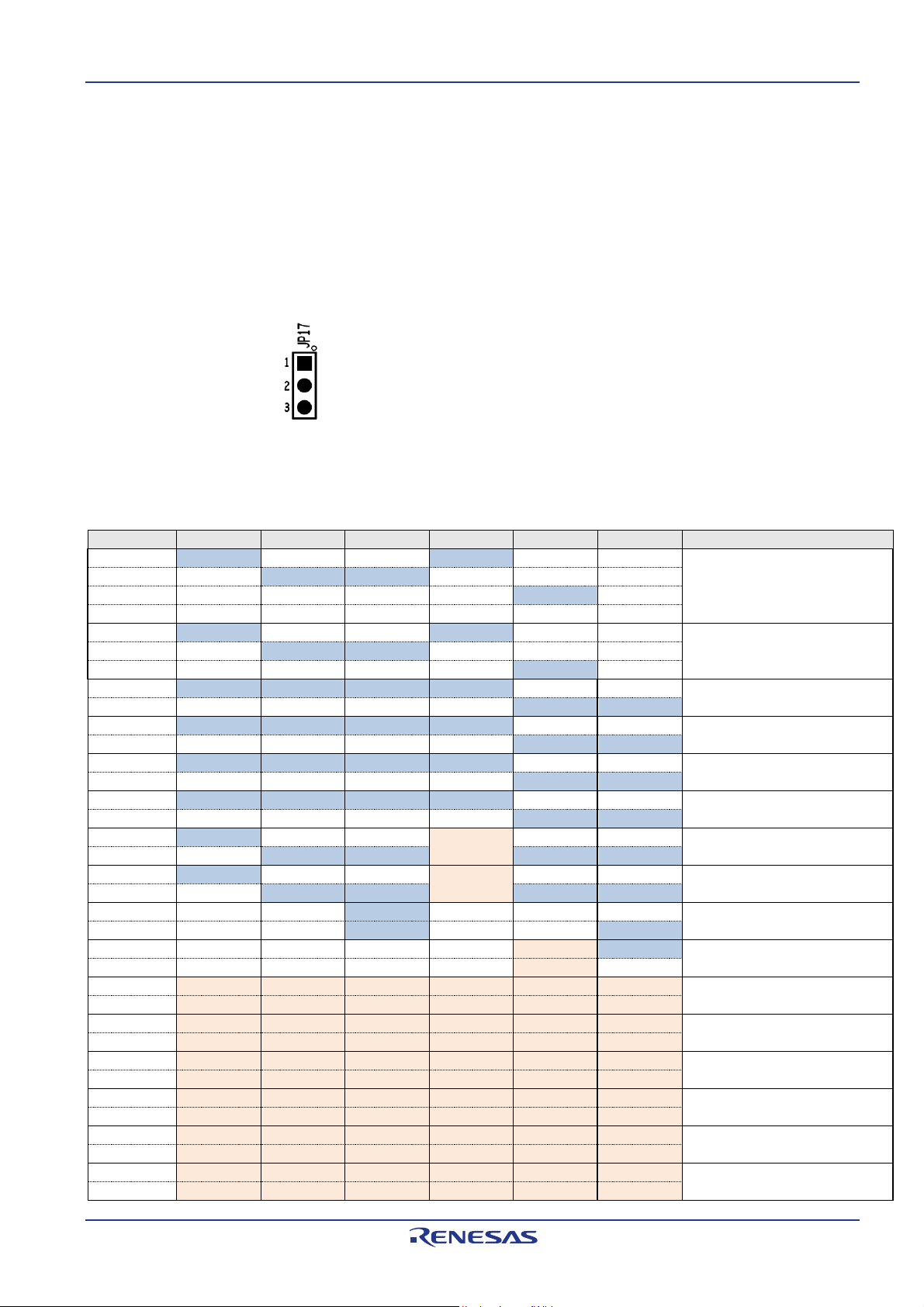
Chapter 3 Jumper Configuration
The function of the board can be configured via jumpers. This chapter describes
the standard configuration, i.e. jumper setting for the intended devices. For the
supported function of the used device, please refer to the corresponding HW
user’s manual.
The table has the following meaning:
x-y: Connect the pins x and y; valid for 3-pin jumpers (e.g. JP17)
The pin #1 can be identified by a small circle in the vicinity of the jumper
Depending on the used device a configuration of several jumpers is required. The
detailed configuration is shown below:
R20UT4148ED0100 Rev. 1.00 8
2017-08-14
Page 9

RH850/F1x-176pin PiggyBack board V4 Y-RH850-F1X-176PIN-PB-T1-V4
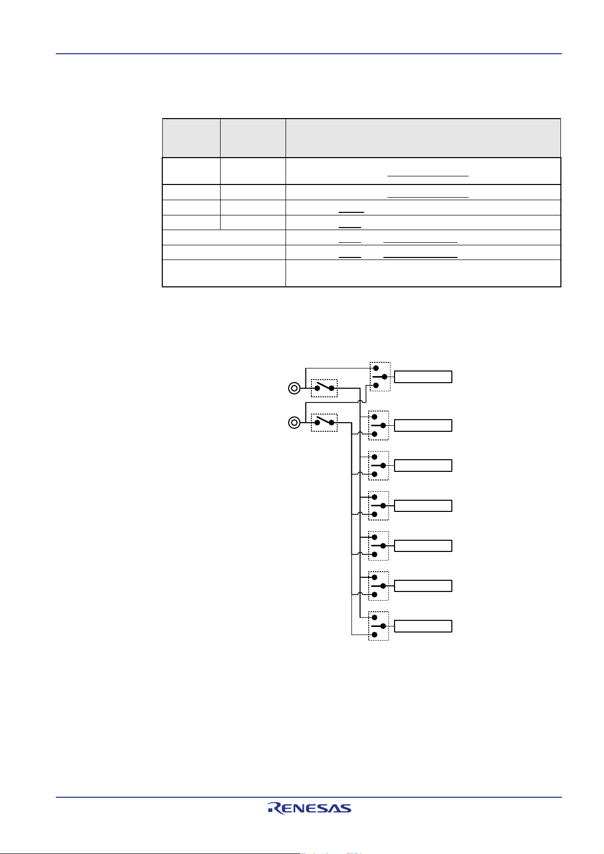
The jumper setting also are shown in this picture:
Figure 3 – Jumper setting overview
The green jumper JP25 for FLMDO0 always must be closed for a ‘normal’
(user mode and debug) operation of the device.
The red jumpers must be set for a single “Voltage 1” (typ +5.0V)
operation of the device.
The blue jumper must be set for a single “Voltage 2” (typ +3.3V)
operation of the device.
The orange jumpers must be selected depending on the used device.
See the printing on the board or the table above for the applicable setting.
For jumper settings related to the device operation mode, refer to the
chapter 8.2.
R20UT4148ED0100 Rev. 1.00 9
2017-08-14
Page 10

RH850/F1x-176pin PiggyBack board V4 Y-RH850-F1X-176PIN-PB-T1-V4
Chapter 4 Power supply
4.1 Board power connection
For operation of the device, a supply voltage must be connected to the board.
Though a single supply voltage is sufficient for the operation of the device, two
(different) voltages can be supplied to the board.
Within this document the following voltages are considered as ‘typical’
connections:
Voltage1 = 5.0V
Voltage2 = 3.3V
The following connectors are available to supply those voltages:
Three 4mm ‘banana-type’ connectors:
- Two red connectors for voltages Voltage1 (CN54) and Voltage2 (CN17).
- A black connector for VSS connection (CN10).
Note: The three connectors are supplied with the board but not assembled.
The E1/E2 emulator that is used for debug purposes and flash programming
can also supply a single operating voltage (‘Dbg_Voltage’).
The voltage is programmable via the E1/E2 GUI as 3.3 or 5.0V (typ).
See the documentation of the E1/E2 and chapter 5 ‘Debug and
Programming interface’ for details.
Note: The E1 voltage is connected to Voltage1, what is typically 5V. Still,
3.3V can be provided by the E1.
In case the PiggyBoard is mounted on a MainBoard, the voltages Voltage1
and Voltage2 are supplied by the on-board regulators of the MainBoard.
NOTE: Do not supply any voltage directly to the PiggyBoard in case it is mounted
on the MainBoard.
For each of the two voltages, ‘Voltage 1 ‘ and ‘Voltage 2’, a green LED (LED1
and LED2) is available to signal that the related voltage is available on the
PiggyBoard.
R20UT4148ED0100 Rev. 1.00 10
2017-08-14
Page 11
RH850/F1x-176pin PiggyBack board V4 Y-RH850-F1X-176PIN-PB-T1-V4
Device
supply
pin
Name on
PiggyBoard
Function
REGVCC
REG0VCC
REG0VDD
Supply for the device internal regulators for the digital logic.
REG1VCC
REG1VDD
Supply for the device internal regulators for the digital logic.
EVCC
EVDD
Supply for ports.
BVCC
BVDD
Supply for ports.
A0VREF
Supply for ports and analog functions of ADC0.
A1VREF
Supply for ports and analog functions of ADC1.
VDDIOF
IO supply voltage for components located on a connected
mainboard.
REG0VCC
JP20
VOLTAGE1
VOLTAGE2
VDDIOF
EVCC
BVCC
A0VREF
A1VREF
JP11
JP12
JP13
JP14
JP15
JP16
JP18
REG1VCC
CN29
4.2 Voltage distribution
The table shows the required device power supply pins and their function:
For each of the above voltages, the voltage source can be selected from
Voltage1 (typ. 5.0V) or Voltage2 (typ. 3.3V) by the jumpers JP12-JP16, JP18,
respectively the jumpers JP11 and JP20.
R20UT4148ED0100 Rev. 1.00 11
2017-08-14
Note:
The RH850/F1KH-D8 device requires a supply voltage of 3.3V on its
REG1VCC pin.
The RH850/F1KM-S4 device requires the same supply voltage to be set to
REG0VCC and REG1VCC.
See the section ‘Electrical Characteristics’ in the device User’s Manual for further
details.
Page 12

RH850/F1x-176pin PiggyBack board V4 Y-RH850-F1X-176PIN-PB-T1-V4
Chapter 5 Clock sources
Four external crystal oscillators for the device clock supply are provided with the
board.
5.1 MainOsc
A crystal or ceramic resonator can be mounted on socket X1.
The applicable frequency range can be found is the devices electrical
specification.
A 8MHz, 16MHz and a 20MHz oscillator is supplied with the board.
5.2 SubOSC
An oscillator with a frequency of 32.768kHz is supplied with the board and can be
soldered into the connector X2.
R20UT4148ED0100 Rev. 1.00 12
2017-08-14
Page 13

RH850/F1x-176pin PiggyBack board V4 Y-RH850-F1X-176PIN-PB-T1-V4
CN19 pin
Device Port
Device signal
1
JP0_2
DCUTCK / LPDCLK
2
GND
GND
3
JP0_4
DCUTRST
4
FLMD0
FLMD0
5
JP0_1
DCUTDO / LPDO
6
P10_8*
FLMD1
7
JP0_0
DCUTDI / LPDI
8
‘Dbg_Voltage’
-
9
JP0_3
DCUTMS
10
JP0_6
EVTO*
11
JP0_5
DCURDY /
LPDCLKOUT
12
GND
-
13
RESET
-
14
GND
-
JP23 pin
Selection for Dbg_Voltage
1-2
5V is selected
2-3
3.3V is selected
Chapter 6 Debug and Programming interface
For connection of the microcontroller debug and flash programming tools, the
connector CN19 is provided.
The signal connection of the connector CN19 is shown in the picture below:
*In case the EVTOUT signal shall be used by the debug/programming tool, the
pin header JP11 must be closed.
The ‘Dbg_Voltage’ (on CN19 pin 8) is monitored or supplied by the debug and
flash programming tools. Therefore, it is necessary to select either Voltage1 (5V)
or the Voltage2 (3.3V) by pin header JP23:
R20UT4148ED0100 Rev. 1.00 13
2017-08-14
Page 14

RH850/F1x-176pin PiggyBack board V4 Y-RH850-F1X-176PIN-PB-T1-V4
Pin
Function
Device Port
Pin
Function
Device Port
1
VOLTAGE1
-
2 VOLTAGE1
-
3
VOLTAGE1
-
4 VOLTAGE1
-
5
RESET
_RESET
6 NMI
P9_0
7
WAKE
-
8 - -
9
INT0
P9_1
10
INT1
P0_6
11
INT2
P9_2
12
INT3
P9_3
13 - -
14 - -
15
UART0TX
P10_10 or
P0_2
16
UART1TX
P0_5
17
UART0RX
P10_9 or
P0_3
18
UART1RX
P0_4
19
LIN0TX
P10_10 or
P0_2
20
LIN1TX
P0_8
21
LIN0RX
P10_9 or
P0_3
22
LIN1RX
P0_7
23
IIC0SDL
P10_3
24
IIC1SDL
P9_1
25
IIC0SDA
P10_2
26
IIC1SDA
P9_0
27
CAN0TX
P10_1 or
P0_0
28
CAN1TX
P0_3
29
CAN0RX
P10_0 or
P0_1
30
CAN1RX
P0_2
31
SENTIN0
P8_0
32
SENTIN1
P9_0
33
SENTOUT0
P8_1
34
SENTOUT1
P9_1
35
PSI50Rx
-
36
PSI51Rx
-
37
PSI50Tx
-
38
PSI51Tx
-
39
PSI50Snyc
-
40
PSI51Sync
-
41
FLX0TX
P11_1
42
FLX0EN
P10_11
43
FLX0RX
P10_14
44
FLXSTPWT
P10_12
45
FLX1TX
P10_8
46
FX1EN
P10_13
Chapter 7 Connectors for ports of device
Connection to each pin of the device is possible via the connectors CN5 to CN8.
Note: The pin headers are directly connected to the pins of the device, therefore
special care must be taken to avoid any electrostatic or other damage to the
device.
7.1 Connectors to MainBoard
Three connectors (CN1 to CN3) are available to connect the PiggyBoard to a
MainBoard.
The signal connection of each connector is described in the following tables:
7.1.1 Connector CN1
R20UT4148ED0100 Rev. 1.00 14
2017-08-14
Page 15

RH850/F1x-176pin PiggyBack board V4 Y-RH850-F1X-176PIN-PB-T1-V4
Pin
Function
Device Port
Pin
Function
Device Port
47
FLX1RX
P10_9
48
FX1CLK
P10_10
49 - -
50 - -
51
ETH0MDIO
P12_4
52
ETH0MDC
P12_5
53
ETH0RXD0
P10_1
54
EH0TXD0
P18_1
55
ETH0RXD1
P10_2
56
EH0TXD1
P18_2
57
ETH0RXD2
P10_4
58
EH0TXD2
P18_3
59
ETH0RXD3
P10_5
60
EH0TXD3
P18_4
61
ETH0RXDCLK
P10_0
62
ETH0TXCLK
P18_7
63
ETH0RXER
P11_14 or
P11_15
64
ETH0TXER
P18_6
65
ETH0CRSDV
P11_12 or
P11_13
66
ETH0TXEN
P18_5
67
ETH0RXDV
P11_11
68
ETH0COL
P11_10
69
ETH0RESET
P2_6
70
ETH0LINK
P18_0
71 - -
72 - -
73
USB0UDMF
-
74
USB0UDMH
-
75
USB0UDPF
-
76
USB0UDPH
-
77 - -
78 - -
79 - -
80 - -
81 - -
82 - -
83 - -
84 - -
85
DIGIO_0
P8_0
86
DIGIO_1
P8_1
87
DIGIO_2
P8_2
88
DIGIO_3
P8_3
89
DIGIO_4
P8_4
90
DIGIO_5
P8_5
91
DIGIO_6
P8_6
92
DIGIO_7
P11_0
93
DIGIO_8
P10_0
94
DIGIO_9
P10_7
95
DIGIO_10
P10_8
96
DIGIO_11
P10_15
97
DIGIO_12
P0_9
98
DIGIO_13
P0_10
99
DIGIO_14
P0_11
100
DIGIO_15
P0_12
101 - -
102 - -
103
MUX0
P10_4
104
MUX1
P10_5
105
MUX2
P10_6
106 - -
107
ADC0
AP0_0
108
ADC1
AP0_1
109
ADC2
AP0_2
110
ADC3
AP0_3
111
ADC4
AP0_4
112
ADC5
AP0_5
113
ADC6
AP0_6
114
ADC7
AP0_7
115
VDDIOF
-
116
VDDIOF
-
117
VOLTAGE2
-
118
VOLTAGE2
-
119
VOLTAGE2
-
120
VOLTAGE2
-
R20UT4148ED0100 Rev. 1.00 15
2017-08-14
Page 16
RH850/F1x-176pin PiggyBack board V4 Y-RH850-F1X-176PIN-PB-T1-V4
Pin
Function
Device Port
Pin
Function
Device Port
1
CAN2Tx
P0_4 2
CAN3Tx
P1_3
3
CAN2Rx
P0_5 4
CAN3Rx
P1_2
5
CAN4Tx
P1_13
6 CAN5Tx
P0_14
7
CAN4Rx
P1_12
8 CAN5Rx
P0_13
9
LIN2Tx
P0_10
10
LIN3Tx
P1_15
11
LIN2Rx
P0_9
12
LIN3Rx
P1_14
13
LIN4Tx
P1_11
14
LIN5Tx
P8_12
15
LIN4Rx
P1_10
16
LIN5Rx
P8_11
17
LIN6Tx
P0_12
18
LIN7Tx
P12_4
19
LIN6Rx
P0_11
20
LIN7Rx
P12_3
21
LIN8Tx
P2_3
22
LIN9Tx
P2_5
23
LIN8Rx
P2_2
24
LIN9Rx
P2_4
25
LIN10Tx
P8_2
26
LIN11Tx
P10_12
27
LIN10Rx
P8_10
28
LIN11Rx
P10_11
29
LIN12Tx
P10_14
30
LIN13Tx
P1_1
31
LIN12Rx
P10_13
32
LIN13Rx
P1_0
33
LIN14Tx
P8_9
34
LIN15Tx
P1_5
35
LIN14Rx
P8_8
36
LIN15Rx
P1_4
37 - -
38 - -
39 - -
40 - -
41 - -
42 - -
43 - -
44 - -
45 - -
46 - -
47
CAN6Tx
P8_1
48
CAN7Tx
P8_3
49
CAN6Rx
P8_0
50
CAN7Rx
P8_4
51 - -
52 - -
53 - -
54 - -
55 - -
56 - -
57 - -
58 - -
59 - -
60 - -
61
LIN16Tx
P11_15
62
LIN17Tx
P8_2
63
LIN16Rx
P12_0
64
LIN17Rx
P8_10
65 - -
66 - -
67 - -
68 - -
69 - -
70 - -
71 - -
72 - -
73 - -
74 - -
75 - -
76 - -
77 - -
78 - -
79 - -
80 - -
81 - -
82 - -
83 - -
84 - -
7.1.2 Connector CN2
R20UT4148ED0100 Rev. 1.00 16
2017-08-14
Page 17

RH850/F1x-176pin PiggyBack board V4 Y-RH850-F1X-176PIN-PB-T1-V4
Pin
Function
Device Port
Pin
Function
Device Port
85 - -
86 - -
87 - -
88 - -
89 - -
90 - -
91 - -
92 - -
93 - -
94 - -
95 - -
96 - -
97 - -
98 - -
99 - -
100 - -
101 - -
102 - -
103 - -
104 - -
105 - -
106 - -
107 - -
108 - -
109 - -
110 - -
111 - -
112 - -
113 - -
114 - -
115 - -
116 - -
117 - -
118 - -
119 - -
120 - -
R20UT4148ED0100 Rev. 1.00 17
2017-08-14
Page 18
RH850/F1x-176pin PiggyBack board V4 Y-RH850-F1X-176PIN-PB-T1-V4
Pin
Function
Device Port
Pin
Function
Device Port
1
PWM00
P10_0
2 PWM01
P10_1
3
PWM02
P10_2
4 PWM03
P10_3
5
PWM04
P10_7
6 PWM05
P10_8
7
PWM06
P10_9
8 PWM07
P10_10
9
PWM08
P9_0
10
PWM09
P9_1
11
PWM10
P0_4
12
PWM11
P0_1
13
PWM12
P0_2
14
PWM13
P0_3
15
PWM14
P8_0
16
PWM15
P8_1
17
PWM16
P10_11
18
PWM17
P10_12
19
PWM18
P10_13
20
PWM19
P10_14
21
PWM20
P9_2
22
PWM21
P9_3
23
PWM22
P8_2
24
PWM23
P8_3
25
PWM24
P10_15
26
PWM25
P11_0
27
PWM26
P11_1
28
PWM27
P11_2
29
PWM28
P11_3
30
PWM29
P11_4
31
PWM30
P11_5
32
PWM31
P11_6
33
PWM32
P11_7
34
PWM33
P9_4
35
PWM34
P9_5 or
P0_11
36
PWM35
P9_6 or
P0_6
37
PWM36
P8_4
38
PWM37
P8_5
39
PWM38
P8_6
40
PWM39
P8_7
41
PWM40
P8_8
42
PWM41
P8_9
43
PWM42
P8_10
44
PWM43
P8_11
45
PWM44
P8_12
46
PWM45
P0_12
47
PWM46
P0_13
48
PWM47
P0_14
49
PWM48
P11_8
50
PWM49
P11_9
51
PWM50
P11_10
52
PWM51
P11_11
53
PWM52
P11_12
54
PWM53
P11_13
55
PWM54
P11_14
56
PWM55
P11_15
57
PWM56
P12_0
58
PWM57
P12_1
59
PWM58
P12_2
60
PWM59
P20_4
61
PWM60
P20_5
62
PWM61
P18_0
63
PWM62
P18_1
64
PWM63
P18_2
65
PWM64
P20_0
66
PWM65
P20_1
67
PWM66
P20_2
68
PWM67
P20_3
69
PWM68
P12_3
70
PWM69
P12_4
71
PWM70
P12_5
72
PWM71
P18_3
73
PWM72
-
74
PWM73
-
75
PWM74
-
76
PWM75
-
77
PWM76
-
78
PWM77
-
79
PWM78
-
80
PWM79
-
81
PWMADC00
AP0_8
82
PWMADC01
AP0_9
7.1.3 Connector CN3
R20UT4148ED0100 Rev. 1.00 18
2017-08-14
Page 19

RH850/F1x-176pin PiggyBack board V4 Y-RH850-F1X-176PIN-PB-T1-V4
Pin
Function
Device Port
Pin
Function
Device Port
83
PWMADC02
AP0_10
84
PWMADC03
AP0_11
85
PWMADC04
AP0_12
86
PWMADC05
AP0_13
87
PWMADC06
AP0_14
88
PWMADC07
AP0_15
89
PWMADC08
AP1_0
90
PWMADC09
AP1_1
91
PWMADC10
AP1_2
92
PWMADC11
AP1_3
93
PWMADC12
AP1_4
94
PWMADC13
AP1_5
95
PWMADC14
AP1_6
96
PWMADC15
AP1_7
97 - -
98 - -
99 - -
100 - -
101 - -
102 - -
103 - -
104 - -
105 - -
106 - -
107 - -
108 - -
109 - -
110 - -
111 - -
112 - -
113 - -
114 - -
115 - -
116 - -
117 - -
118 - -
119 - -
120 - -
R20UT4148ED0100 Rev. 1.00 19
2017-08-14
Page 20

RH850/F1x-176pin PiggyBack board V4 Y-RH850-F1X-176PIN-PB-T1-V4
Chapter 8 Other circuitry
8.1 Push button for RESET
In order to issue a RESET to the device, the push-button SW1 is available.
8.2 Mode Selection
The PiggyBack Board gives the possibility to configure the following mode pins
FLMD0 via jumper JP25
FLMD1 via jumper JP19
MODE0 via jumper JP28
MODE1 via jumper JP26
MODE2 via jumper JP27
To apply “High” or “Low” to the mode pins, the pins 1 and 2, or the pins 2 and 3
(if available) of the corresponding jumper must be closed, respectively.
Note: Pin 1 of all jumpers is marked by a small circle.
CAUTION: Be careful in configuration of mode related pins. Wrong configuration
and operation of the device outside of its specification can cause irregular
behaviour of the device and long term damage cannot be excluded. Be sure to
check the corresponding User’s Manual for details, which modes are specified for
the used device
Note:
In the very most cases the ‘Normal operating mode’ of the device will be used.
This mode is for execution of the user program. The on-chip debug functions also
use this mode.
To select the ‘Normal operating mode’ of the device, the FLMD0 pin must be
pulled low. To do so, close the pins 2-3 on the jumper JP25:
All other jumper related to the mode selection can be left open.
R20UT4148ED0100 Rev. 1.00 20
2017-08-14
Page 21

RH850/F1x-176pin PiggyBack board V4 Y-RH850-F1X-176PIN-PB-T1-V4
8.3 Signalling LEDs
Eight LEDs are provided to allow visual observation of the output state of device
port pins. Device pins P8_0 to P8_7 are connected to the even pins 2 to 16 of the
pin header CN24, while the LEDs 1 to 8 are connected to the odd pins 1 to 15,
respectively.
Thus the LEDs can be either connected to
the device port pins P8_0 to P8_7 by closing the connection on CN24 using a
jumper, or
any device port pin by using the provided wire connections.
R20UT4148ED0100 Rev. 1.00 21
2017-08-14
Page 22

RH850/F1x-176pin PiggyBack board V4 Y-RH850-F1X-176PIN-PB-T1-V4
100,00mm
160,00mm
CN2
CN1
24,00mm
24,00mm
CN3
9,00mm
CN4
9,00mm
80,00mm
50,00mm
Chapter 9 Mechanical dimensions
R20UT4148ED0100 Rev. 1.00 22
2017-08-14
Page 23

RH850/F1x-176pin PiggyBack board V4 Y-RH850-F1X-176PIN-PB-T1-V4
P11<13>
PIN72
REG0VCC
REG0VCC
P11<14>
P11<14>RH850/F1K ECO, ADVANCED, PREMIUM (named F1K)
ISOVCL
(name F1KH )
P11<13>
P11<13>
P11<13>
RH850/F1M ECO, ADVANCED (named F1M) P11<14>
PIN60
RH850/F1L ECO ADVANCED, PREMIUM (named F1L)
(name F1KM )
ISOVCL
P11<14>
PIN14PIN13
RH850/F1H ECO, PREMIUM (named F1H)
PIN114
P9<6>
ISOVSS
ISOVCL
P9<5>
ISOVSS
REG1VCC
(F1L, F1M, F1H, F1K)
(F1L, F1M, F1H, F1K)
(F1KM),F1KH)
(F1KM),F1KH)
P1<7>
P1<6> (F1L, F1M, F1H, F1K)
(F1L, F1M, F1H, F1K)
(F1KM),F1KH)
(F1KM),F1KH)
(F1KM),F1KH)
(F1M, F1H)
(F1L, F1K)
(F1KM)
(F1KH)
(F1M, F1H)
(F1L, F1K)
P1<7>
P1<7>
P1<6>
P1<6>
PIN73
P9<5>
ISOVCL
PIN113
REG0VCCREG0VCC
REG0VCC
REG0VCC
REG0VCCISOVSS
ISOVSS ISOVSS
P1<7>
P1<7>
ISOVSS
P1<6>
ISOVCL
P1<6>
ISOVCL ISOVSS
P9<6>
ISOVSS
Rh850/F1KM SC160/SC240
MAIN_OSCILLATOR
32.686KHZX2SUB_OSCILLATOR
Rh850/F1KH
1
Fri Jun 30 10:46:16 2017 PAGE 1 OF 4
Rh850_F1X_176pin_PB_T1_V4
1.00
EESS-0400-157-01
Electronics Europe GmbH
147
148
149
150
158
160
162
97
124
111
90
54
100n
100n
100n
100n
100n
100n
100n
100n 100n100n100n 100n100n100n100n100n
3.3 OR 5V
141
151
152
153
REG0VCC
3.3 OR 5V
3.3 OR 5V
REG1VCC
REG0VCC
75
74
70
69
11
0
8181
64
63
60
104
103
102
101
64
58565553506354
44
43
42
41
44
34
24
22
20
17
15
60
3.3 OR 5V
173
163
15
RH850_F1L_176_YAM_SOCKET
133
A1VREF
6
68
62
45
66
65
55
129
134
133
107
15
16
5
7
112
112
117
114
113
109
3
8
124
116
114
123
146
149
128
172
12
58
73
77
8080
72
8795
73
71
82
78
7
9
10
61
3
0
13
12
12
13
14
16
4
17
2
1
202061574513
2131412118976675431
2
121314
15
3.3 OR 5V
BVCC EVCC
0
1
3
4
5
3
4
5
1
1
2
3
4
2
3
4
176
175
170
169
176
174
175
171
169
170
168
167
166
165
164
161
167
168
166
165
159
160
9
8
11
10
565
6
7
898
9
101110
11
14
18
19
19
212221
23
24
23
6
11
12
13
14
0
1
2
3
12
13
6
2
10
11
12
252625
26
282928
29
30
30
313231
32
333433
35
35
5
4
3
363736
37
383938
39
40
40
41
42
43
4
45464748495152
57
61
62
46
474849505152535456
57
157
156
155
154
153
157
158
156
154
155
151
152
150
148
145
143
142
140
139
138
146
147
144
145
141
142
139
140
138
137
136
135
134
137
136
135
132
131
130
129
127
126
125
123
122
121
120
119
118
117
115
113
111
110
132
131
130
1
2
3
4
128
126
125
5
6
7
9
122
121
120
119
10
4
5
118
116
115
111
110
109
0
1
2
4
3
2
1
108
107
106
105
100
99
98
97
96
95
94
93
92
91
90
89
66676869707172
76
79
83
65
67
7576778283
8485868788
8485868788
108
106
105
104
103
102
101
100
0
0
1
2
3
4
5
6
7
8
98
97
96
95
94
93
92
91
90
89
9
10
11
12
13
14
15
3.3 OR 5V
210
1
0
11
10
9
8
0
SOCKET 2WAY
16.000 MHZ + SOCKET
18PF
3
2
445
14
15
0134567
8
3.3 OR 5V
AWOVCL
10
176
174
172
170
166
164
168
162
160
156
154
158
152
150
148
146
144
142
140
138
134
136
HEADER 44WAY
175
173
171
169
167
165
163
161
159
157
155
153
151
149
147
145
143
141
139
137
135
133
5355514947
45
878583817977757371696765636159
57
131
129
127
125
123
121
119
117
115
113
109
107
105
103
101
99
124
126
128
132
130
114
116
118
120
122
104
106
108
110
112
949698
100
102
89
91
41433739313527
2921232517191513119753
1
92
4442343238
40
22
242628
30
HEADER 44WAY
141618
20
284
6
10
888684828078767472706866646260585652504846
A1VREF
3.3 OR 5V3.3 OR 5V
144
HEADER 44WAY
93
95
36
12
143
27
20
174
173
172
171
33
0
A0VREF
18
127
47K
9
159
161
162
163
164
3.3 OR 5V
A0VREFBVCC
3.3 OR 5V
EVCC
3.3 OR 5V
HEADER 44WAY
27
99
REG0VCC
ISOVCL
ISOVCL
ISOVCL
ISOVCL
5959
0
74
78
12p 12p12p 12p
JP9
C23
JP31
C22
C12
C21
JP10
JP8
JP7
JP6
JP5
JP4
JP1
JP2
JP3
C11
R12
R10
R11
CN21
C18
IC1
C17
C16
CN8CN7
CN6CN5
C14C13C5 C9C8C4C2C1
C6C3 C10C7
X1
P10<15..0>
select_113
P11<14>
Z_PINS<176..1>
P10<15..0>
Z_PINS<176..1>
Z_PINS<176..1>
P9<6> select_114
AP1<15..0>
P1<15..0>
select_72
P0<15..0>
P0<15..0>
select_13
select_14
RESET_Z
select_113
select_73
P10<15..0>
P12<5..0>
P11<15..0>
P2<6..0>
P8<12..0>
P1<15..0>
P20<5..0>
P9<6..0>
FLMD0
P2<6..0>
P1<15..0>
P8<12..0>
select_114
Z_PINS<176..1>
P18<7..0>
P11<15..0>
P12<5..0>
AP0<15..0>
P2<6..0>
JP0<6..0>
P9<5>
P11<13>
select_73
select_72
select_14
select_13
P2<6..0>
P1<15..0>
JP0<6..0>
Z_PINS<176..1> Z_PINS<176..1>
21
3
2
1
321
321
321
212121
212121
21
56
616254
60
119
120
115
116
117
118
150
149
148
147
146
145
144
143
17
16
15
171
170
169
168
14
13
12
11
10
9
8
167
166
165
164
163
162
161
7
6
160
159
158
157
156
155
154
153
152
3
2
1
176
175
174
114
113
112
111
110
109
108
41
40
39
888786858483823881
803677
76
64
65
48
49
79
78
35
34
505152
53
727374
75
33
32
31
30
29
28
27
26
67
686970
25
24
23
21
20
19
18
66
42
43
44
454647
142
141
57
63
107
71
37
121
55
22
173
151
5
172
140
4
58
59
134
135
136
137
122
123
124
125
126
127
128
129
130
131
132
133
91
92
93
94
95
96
97
98
99
100
101
102
103
104
105
106
139
138
89
90
4443
4241
4039
3837
3635
3433
3231
3029
2827
2625
2423
2221
2019
1817
1615
1413
1211
10987654321
4443
4241
4039
3837
3635
3433
3231
3029
2827
2625
2423
2221
2019
1817
1615
1413
1211
10987654321
4443
4241
4039
3837
3635
3433
3231
3029
2827
2625
2423
2221
2019
1817
1615
1413
1211
10987654321
4443
4241
4039
3837
3635
3433
3231
3029
2827
2625
2423
2221
2019
1817
1615
1413
1211
10987654321
JP0[6]
P10[2]
P10[1]
P10[0]
BVSS[2]
BVDD[2]
P12[2]
P12[1]
P12[0]
P11[15]
P11[7]
P11[6]
P11[5]
P11[4]
P11[3]
P11[2]
P11[1]
P10[14]
P10[13]
P10[12]
P10[11]
P10[10]
P10[9]
P10[8]
P10[7]
P10[6]
BVSS[1]
P18[7]
P18[6]
P18[5]
P18[4]
P18[3]
P18[2]
P18[1]
P18[0]
ISOVSS
ISOVDD
BVDD[1]
A1VSS
A1VREF
AP1[12]
AP1[13]
AP1[14]
AP1[15]
AP1[0]
AP1[1]
AP1[2]
AP1[3]
AP1[4]
AP1[5]
AP1[6]
AP1[7]
AP1[8]
AP1[9]
AP1[10]
AP1[11]
EVDD[2]
P20[4]
P20[5]
P20[0]
P20[1]
P20[2]
P20[3]
P9[6]
P9[5]
P9[4]
P9[3]
P9[2]
P9[1]
P9[0]
EVSS[2]
AP0[0]
AP0[1]
AP0[2]
AP0[3]
AP0[4]
AP0[5]
AP0[6]
AP0[7]
AP0[8]
AP0[9]
AP0[10]
AP0[11]
AP0[12]
AP0[13]
AP0[14]
AP0[15]
A0VREF
A0VSS
P8[9]
P8[8]
P8[7]
P8[6]
P8[5]
P8[4]
P8[3]
P8[1]
P8[0]
P1[15]
P1[14]
P2[5]
P2[4]
P1[4]
P1[5]
P1[6]
P1[7]
EVSS[1]
P0[7]
P0[8]
P0[9]
P0[10]
P2[2]
P2[3]
FLMD0
X1
X2
REGVDD
AWOVDD
AWOVSS
IP0[0]
XT1
EVDD[1]
RESET*
P1[8]
P1[9]
P1[10]
P1[11]
P2[0]
P2[1]
JP0[0]
JP0[1]
JP0[2]
JP0[3]
JP0[4]
JP0[5]
P8[12]
P8[11]
P8[10]
P8[2]
EVSS[0]
P2[6]
P1[13]
P1[12]
P1[3]
P1[2]
P1[1]
P1[0]
P0[14]
P0[13]
P0[12]
P0[11]
P0[6]
P0[5]
P0[4]
EVDD[0]
P0[3]
P0[2]
P0[1]
P0[0]
P12[5]
P12[4]
P12[3]
P11[14]
P11[13]
P11[12]
P11[11]
P11[10]
P11[9]
P11[8]
P11[0]
P10[15]
BVSS[0]
BVDD[0]
P10[5]
P10[4]
P10[3]
2
1
BI
321
321
321
3
2
1
2
1
212
1
2
1
212
1
BIBIBI
BI
BI
BI
BI
BI
BI
BI
BI
BI
BI
IN
IN
BI
BI
BI
BI
BIBIBI
BI
BI
BI
BI
BIBIBI
BI BI
BIBI
34 44
14 24
403836343230282624222018161412
10
864
2
3937353331292725232119171513119753
1
34 44
14 24
403836343230282624222018161412
10
864
2
3937353331292725232119171513119753
1
34 44
14 24
40
383634323028262422201816141210
8
642
39
373533312927252321191715131197531
34 44
14 24
40
383634323028262422201816141210
8
642
39
373533312927252321191715131197531
2
1
Size Document Num ber
A2
Title
Date:
987654321
987654321
A
B
C
D
E
F
A
B
C
D
E
F
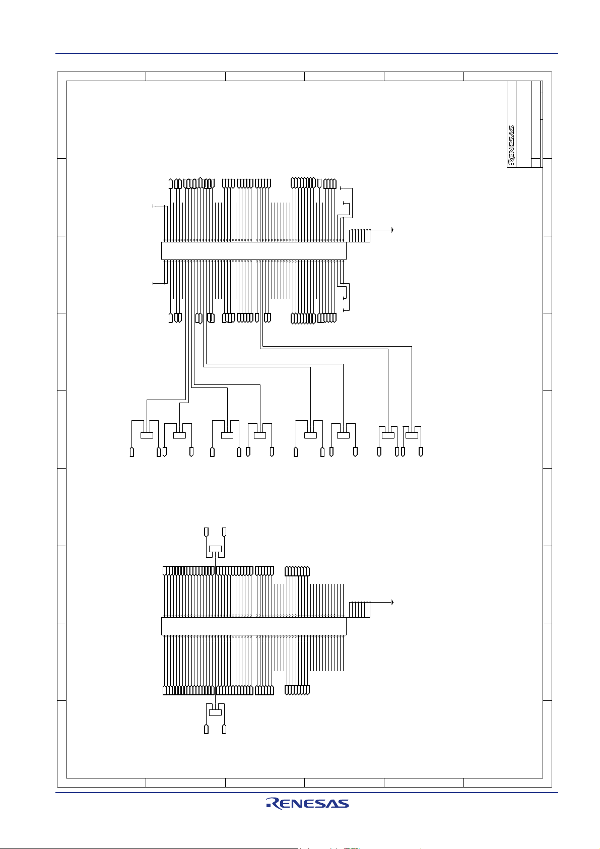
Chapter 10 Schematic
R20UT4148ED0100 Rev. 1.00 23
2017-08-14
Page 24

RH850/F1x-176pin PiggyBack board V4 Y-RH850-F1X-176PIN-PB-T1-V4
DEBUG AND PROGRAMMING INTERFACE VOLTAGE DISTRIBUTION
TOP
FUDUCIALS AND GROUND TEST POINTS
ALLOWED DC SUPPLY
OVERVOLTAGE PROTECTION
MAX 3.3V
ALLOWED DC SUPPLY
TO BE PRINTED ON PCB
MAX 5V
PUSH BUTTON FOR RESET
RUBBER FEET
BOTTOM
LED - P8<7..0>
TO BE PRINTED ON PCB
Thu Jun 29 12:45:02 2017 PAGE 2 OF 4 1.00
EESS-0400-157-01
Rh850_F1X_176pin_PB_T1_V4
Electronics Europe GmbH
SMA STRAIGHT
1SMA5919BT3G_5.6V
N.A.
TESTPOINT_SMALL_RD
5V
V5V_SELECT
p5v0p5v0
10n
A1VREF
MF-USMF020
VIN_3.3V
VIN_5V
p3v3
3.3V5.0V
p3v3
3.3V
p5v0
5.0V
N.A.
3.3 OR 5V
EVCC
yellow
NXP_BC847C
header 16way
3.3 OR 5V
3.3 OR 5V
TESTPOINT_SMALL_RD
GREEN
VDDIOF
3.3 OR 5V
EVCC
3.3 OR 5V
PUSH BUTTON 4 PIN SMD
10K
EVCC
3.3 OR 5V
1N4148W-V
REG1VCC
REG0VCC
V3V_SELECT
3.3 OR 5V
A0VREF
3.3 OR 5V
3.3 OR 5V
BVCC
3.3V
3.3V
p3v3
5.0V
8
6
10K
3.3 OR 5V
EVCC
10K
2
47K
3
501
4
51
0
0
NXP_BC847C
6534721
0
56K
yellow
MF-USMF020
56K
10K
1K5
56K
10K
NXP_BC847C
1K5
10K
56K
10K
yellow
56K
NXP_BC847C
1K5
yellow
10K
NXP_BC847C
1K5
10K
1K5
56K
NXP_BC847C
1K5
56K
10K
NXP_BC847C
1K5
yellow
56K
10K
NXP_BC847C
1K5
yellow yellow yellow
3.3 OR 5V
EVCC
N.A.
STD POWER LAB SOCKET 4MM RED
N.A.
STD POWER LAB SOCKET 4MM BLACK
N.A.
STD POWER LAB SOCKET 4MM RED
5V
GREEN
51
150
TESTPOINT_SMALL_RD
RUBBER FOOT D=11.1MM/H=5MM GREY
RUBBER FOOT D=11.1MM/H=5MM GREY
RUBBER FOOT D=11.1MM/H=5MM GREY
RUBBER FOOT D=11.1MM/H=5MM GREY
RUBBER FOOT D=11.1MM/H=5MM GREY
GND-TESTPOINT
GND-TESTPOINT
GND-TESTPOINT
FIDUCIAL_1MM
FIDUCIAL_1MM
GND-TESTPOINT
GND-TESTPOINT
GND-TESTPOINT
FIDUCIAL_1MM
FIDUCIAL_1MM
1SMA5919BT3G_5.6V
3.3V
1SMA5914BT3G_3.6V
HEADER 14WAY SHROUDED
100u
100u
JP29
R17
JP22
R7
JP23
JP20
JP18
JP16
JP15
JP14
JP13
LED9
R73
TR4
R71
R69
LED13
R74
TR8
R72
R70
LED8
R67
TR3
R44
R42
LED12
R68
LED7
R40
TR2
R36
R38
LED11
R41
TR7
R45
R43
CN24
TR6
R39
R37
LED6
R34
TR1
R32
LED10
R35
R23
TR5
R33
R31
MP1
MP2
MP3
MP4
MP5
TP3
TP4
TP5
TP6
C20
C19
R3
D2
D3
D4
C15
R5
R8
R9
R2
CN10
D1
LED2
R6
TP13
TP2
TP1
FU2
FU1
TP12
TP11
TP10
TP9
TP8
TP7
LED1
CN17
CN19
CN9
CN54
SW1
R1
JP11
JP12
RESET_Z
Port7Port6Port5Port4
Port2 Port3Port1Port0
Port0
Port7
Port6
Port5
Port4
Port3
Port2
Port1
RESET_Z
FLMD0
JP0<0..6>
P10<15..0>
JP0<0..6>
LXL2
P8<12..0>
321
2
1
321
21
321
32132132132
1
2
3
1
2
3
1
2
3
1
2
3
1
2
3
1
16 15
14 13
12 11
10 9
8 7
6 5
4 3
2 1
2
3
1
2
3
1
2
3
1
111
1
2
1
1
1
1
11111
1
2
1
1413
1211
10987654321
1
5
4
3
2
2
1
21
321
321
OUT
OUT
OUT
BI
BI
ININININ
ININININ
OUT
OUT
OUT
OUT
OUT
OUT
OUT
OUT
321
BI
2
1
321
2
1
321
32132132132
1
B
E
C
B
E
C
B
E
C
B
E
C
B
E
C
16 15
14 13
12 11
10 9
8 7
6 5
4 3
2 1
B
E
C
IN
B
E
C
B
E
C
2
1
31 41
11 21
9 01
864
2
753
1
Size Docu ment Number
A2
Title
Date:
987654321
987654321
A
B
C
D
E
F
A
B
C
D
E
F
R20UT4148ED0100 Rev. 1.00 24
2017-08-14
Page 25
RH850/F1x-176pin PiggyBack board V4 Y-RH850-F1X-176PIN-PB-T1-V4
PWM59
PWM14
-
-
PWMADC11
PWMADC01
PWM75
PWM73
PWM71
PWMADC1
PWM48
VDDB
-
PWM51
PWMADC15
PWM36
ETH0TXER
USB0UDMF-USB0UDPF
ETH0MDIO
ETH0RXDV
PWM01
PWM05
PWM11
PWM47
PWM49
PWM53
PWM55
PWM57
PWM69
PWM67
PWM65
PWM61
PWM63
PWMADC03
ETH0RXD3
DIGIO_12
DIGIO_10
DIGIO_8
DIGIO_6
DIGIO_4
-
SENTIN0
PWM46
SENTOUT0
PSI50Rx
VDDB
-
MUX2
MUX0
ADC0
ADC2
VDDIOF
ADC4
ADC6
DIGIO_14
--DIGIO_2
DIGIO_0
-
ETH0RXDCLK
ETH0RESET
ETH0RXD2
FLX0TX
PSI50Snyc
PSI50Tx
FLX1RX
ETH0RXD1
FLX0RX
FLX1TX
ETH0RXD0
IIC0SDL
IIC0SDA
VDDA
CONNECTOR1
VDDB
VDDB
VDDIOF
ADC7
--MUX1
ADC1
ADC3
ADC5
DIGIO_13
DIGIO_15
DIGIO_7
DIGIO_5
DIGIO_3
DIGIO_1
DIGIO_9
DIGIO_11
---
-
USB0UDPH
-
EH0TXD3
ETH0TXCLK
USB0UDMH
ETH0COL
ETH0LINK
EH0TXD2
-
--
EH0TXD1
FLXCLK
FLX0EN
FX1EN
EH0TXD0
PSI51Sync
PSI51Tx
ETH0MDC
FLXSTPWT
LIN1TX
SENTIN1
LIN1RX
CAN1RX
PSI51Rx
CAN1TX
IIC1SDA
IIC1SDL
UART1RX
SENTOUT1
-
VDDA
NMI-INT1
VDDA
INT3
UART1TX
-
-----
-----
PWMADC1
PWMADC1
PWMADC0
PWMADC0
PWMADC0
PWMADC0
PWMADC0
PWM78
PWM76
PWM74
PWM72
PWM58
PWM50
PWM40
PWM34
PWM70
PWM68
PWM66
PWM64
PWM62
PWM60
PWM56
PWM54
PWM52
PWM42
PWM16
PWM18
PWM30
PWM22
PWM28
PWM32
PWM26
PWM00
PWM02
PWM12
PWM08
PWM06
PWM77
PWM79
PWMADC09
PWMADC13
PWM43
PWM45
PWM37
PWM35
PWM23
PWM25
PWM27
PWM09
PWM31
PWM03
PWM15
PWM29
PWM10
PWM19
PWM17
PWM13
PWM38
PWM07
PWM04
PWM24
PWM21PWM20
PWM33
CONNECTOR3
ETH0TXEN
RESET
WAKE
INT0
INT2-UART0TX
UART0RX
UART0RX
LIN0TX
LIN0RX
CAN0TX
CAN0TX
CAN0RX
CAN0RX
ETH0RXER
ETH0RXER
ETH0CRSDV
ETH0CRSDV
PWM41
PWM39
PWM44
PWMADC05
PWMADC07
LIN0RX
LIN0TX
VDDA
UART0TX
MAIN BOARD CONNECTORS
Thu Jun 29 12:45:03 2017 PAGE 3 OF 4 1.00
EESS-0400-157-01
Rh850_F1X_176pin_PB_T1_V4
Electronics Europe GmbH
QSH-060-01-F-D-AQSH-060-01-F-D-A
5.0V
3.3V
3.3 OR 5V
VDDIOF
3.3 OR 5V
VDDIOF
3.3V
5.0V
JP33
JP32
CN1
JP36
JP34
JP24
JP30
JP37
JP35
JP17
CN3
JP21
LIN0TX
LIN0RX
CAN0TX
CAN0RX
ETH0RXER
ETH0CRSDV
AP1<3>
AP1<1>
NC
P0<2>
P11<13>
P18<6>
RESET_Z
NC
P9<1>
P9<2>
NC
NC
NC
P11<1>
P10<14>
P10<9>NCP12<4>
P10<1>
P10<2>
P10<4>
P10<5>
P10<0>
NCNCNCNCNCNCNC
P8<0>
P8<2>
P8<4>
P8<6>
P10<0>
P10<8>
P0<9>
P0<11>
P9<0>
NC
P0<6>
P9<3>NCP0<5>
P0<4>
P0<8>
P0<7>
P9<1>
P9<0>
P0<3>
P0<2>
P9<0>
P9<1>
NCNCNC
P10<11>
P10<12>
P10<13>
P10<10>NCP12<5>
P18<1>
P18<2>
P18<3>
P18<4>
P18<7>
P18<5>
P11<10>
P18<0>
NCNCNCNCNC
NC
P8<1>
P8<5>
P11<0>
P10<7>
P10<15>
P0<10>
P0<12>
NC NC
P10<4> P10<5>
P10<6> NC
AP0<0> AP0<1>
AP0<2> AP0<3>
AP0<4> AP0<5>
AP0<6> AP0<7>
P11<0>
P11<4>
P18<3>
NCNCNC
NC
AP0<12>
P8<12>
P8<10>
AP1<6>
AP1<4>
AP0<14>
AP1<0>
AP0<10>
AP0<8>
P20<2>
P12<3>
P20<0>
P18<1>
P12<2>
PWM34
P12<0>
P11<12>
P11<10>
P11<8>
P8<8>
P8<4>
P11<7>
P11<3>
P11<1>
P8<2>
P9<2>
P10<13>
P10<11>
P8<0>
P0<4>
P9<0>
P10<2>
NC
NC
NCNC
NCNCNC
NCNC
NCNC
NCNC
NCNCNCNC
AP0<15>
P12<4>
P18<2>
P20<4>
P12<1>
P11<15>
P11<13>
P0<12>
P8<11>
PWM35
P11<6>
P8<3>
P8<1>
P0<3>
P0<1>
P9<1>
P10<10>
P10<3>
P10<1>
NC
NCNCNC
NC
P10<0>
P9<6>
P10<8>
P10<14>
P10<12>
AP0<11>
P20<3>
P18<0>
P11<2>
AP0<9>
AP0<13>
AP1<5>
AP1<7>
P0<13>
P20<1>
P12<5>
NC
P20<5>
P9<4>
NC
P0<2>
P11<14>
P11<9>
P10<9>
P10<10>
P0<3>
NC
AP1<2>
P0<11>
P8<6>
P8<9>
P8<7>
P10<7>
P9<5>
P10<15>
P9<3>
P0<2>
P10<9>
P0<3>
P10<0>
P0<1>
P11<14>
P11<15>
P11<12>
NC
NC
P8<5>
P0<6>
P8<3>
NC
P10<10>
P10<8>
NC
P8<1>
P8<0>
P2<6>
P11<11>
P10<3>
P10<2>
UART0RX
UART0TX
P11<11>
P0<14>
P11<5>
P10<9>
P0<0>
P10<1>
321
321
128
127
126
125
124
123
122
121
120119
118117
116115
114113
112111
110109
108107
106105
104103
102101
10099
9897
9695
9493
9291
9089
8887
8685
8483
8281
8079
7877
7675
7473
7271
7069
6867
6665
6463
6261
6059
5857
5655
5453
5251
5049
4847
4645
4443
4241
4039
3837
3635
3433
3231
3029
2827
2625
2423
2221
2019
1817
1615
1413
1211
10987654321
3
2
1
3
2
1
321
321
3
2
1
3
2
1
321
128
127
126
125
124
123
122
121
120119
118117
116115
114113
112111
110109
108107
106105
104103
102101
10099
9897
9695
9493
9291
9089
8887
8685
8483
8281
8079
7877
7675
7473
7271
7069
6867
6665
6463
6261
6059
5857
5655
5453
5251
5049
4847
4645
4443
4241
4039
3837
3635
3433
3231
3029
2827
2625
2423
2221
2019
1817
1615
1413
1211
10987654321
321
321
OUT
321
IN
OUT
OUT
321
INININ
OUT
IN
IN
IN
IN
INININININ
IN
OUT
IN
IN
IN
IN
128
127
126
125
124
123
122
121
120119
118117
116115
114113
112111
110109
108107
106105
104103
102
101
100
9896949290888684828078
767472706866646260585654525048464442403836343230282624222018161412
10
864
2
9997959391898785838179777573716967656361595755535149474543413937353331292725232119171513119753
1
IN
IN
IN
IN
IN
OUT
INININ
IN
IN
INININ
IN
IN
OUT
IN
INININ
OUT
OUT
OUT
OUT
OUT
OUT
OUT
OUT
OUT
INININ
IN
IN
IN
IN
IN
OUT
IN
IN
IN
INININ
IN
IN
IN
321
OUT
IN
INININININININ
IN
OUT
321
IN
IN
IN
3
2
1
OUT
IN
OUT
OUT
OUT
IN
OUT
IN
IN
OUT
IN
IN
BI
OUT
OUT
IN
128
127
126
125
124
123
122
121
120119
118117
116115
114113
112111
110109
108107
106105
104103
102
101
100
9896949290888684828078
767472706866646260585654525048464442403836343230282624222018161412
10
864
2
9997959391898785838179777573716967656361595755535149474543413937353331292725232119171513119753
1
INININININININ
INININ
IN
IN
IN
INININ
BI
BIBIBI
BI
BI
BIINBI
IN
OUT
OUT
OUT
OUT
IN
OUT
OUT
IN
IN
BI
OUT
IN
321
IN
IN
321
IN
IN
IN
IN
OUT
IN
OUT
OUT
OUT
OUT
OUTINOUT
OUT
OUT
OUT
BIBIBI
BI
BI
BI
IN
BI
BI
IN
IN
OUT
OUT
OUT
OUT
321
OUTINOUT
OUT
321
OUT
OUT
OUT
Size Docu ment Number
A2
Title
Date:
987654321
987654321
A
B
C
D
E
F
A
B
C
D
E
F
R20UT4148ED0100 Rev. 1.00 25
2017-08-14
Page 26

RH850/F1x-176pin PiggyBack board V4 Y-RH850-F1X-176PIN-PB-T1-V4
MAIN BOARD CONNECTORS
MODE0 MODE2MODE1FLMD1
MODE Jumper
LIN13Tx RLIN33
LIN13Rx RLIN33
CAN5Rx
CAN5Tx
CAN3Rx
CAN3Tx
LIN3Tx RLIN23
LIN5Rx RLIN25
LIN7Tx RLIN27
LIN9Tx RLIN29
LIN9Rx RLIN29
LIN11Tx RLIN31
LIN11Rx RLIN31
LIN7Rx RLIN27
LIN5Tx RLIN25
LIN3Rx RLIN23
CONNECTOR2
LIN4Rx RLIN24
LIN4Tx RLIN24
LIN2Rx RLIN22
LIN6Rx RLIN26
LIN8Tx RLIN28
LIN8Rx RLIN28
LIN6Tx RLIN26
LIN2Tx RLIN22
LIN10Tx RLIN37
LIN10Rx RLIN37
LIN12Rx RLIN32
LIN12Tx RLIN32
CAN4Tx
CAN2Rx
CAN2Tx
CAN4Rx
CAN7Rx
CAN9Tx
CN11Tx
CN11Rx
CAN9Rx
CAN7Tx
MLBDAT
MLBRESET
LIN15Tx RLIN35
LIN17Tx RLIN37
LIN17Rx RLIN37
LIN19Tx RLIN210
LIN19Rx RLIN210
LIN20Tx RLIN212
LIN15Rx RLIN35--
-
LIN20Rx RLIN212
ETNB1TXERR
ETNB1TXCLK
ETNB1TXD2
ETNB1TXD1
ETNB1TXD3
MMCA0DAT1
MMCA0DAT3
MMCA0DAT5
MMCA0DAT7
ETNB1MDC
ETNB1TXD0
MMCA0CMD
SFMA0IO3
SFMA0IO1
SFMA0SSL
LIN23Tx RLIN214
LIN23Rx RLIN214
LIN24Rx RLIN215
-
LIN14Tx RLIN34
LIN14Rx RLIN34
LIN18Tx RLIN20
LIN20Tx RLIN211
LIN18Rx RLIN20
LIN16Rx RLIN36
LIN16Tx RLIN36
CAN8Tx
CAN6Rx-MLBCLK
MLBSIG
CAN6Tx
CAN10Rx
-
CAN10Tx
CAN8Rx
LIN20Rx RLIN211
ETNB1RXERR
ETNB1RXCLK
ETNB1RXD0
ETNB1RXD1
ETNB1RXD2
ETNB1MDIO
MMCA0DAT6
MMCA0DAT2
MMCA0DAT0
MMCA0DAT4
ETNB1RXD3
MMCA0CLK
SFMA0IO2
SFMA0CLK
SFMA0IO0
LIN24Tx RLIN215
LIN22Tx RLIN213
LIN22Rx RLIN213
-
-
ETNB1COL
ETNB1LINK
ETNB1TXEN
-
ETNB1CRSDV
ETNB1RXDV
ETNB1RESET-
CONNECTOR4
Thu Jun 29 12:45:03 2017 PAGE 4 OF 4 1.00
EESS-0400-157-01
Rh850_F1X_176pin_PB_T1_V4
Electronics Europe GmbH
QTH-060-01-F-D-A
N.A.
QTH-060-01-F-D-A
621
EVCC
3.3 OR 5V
EVCC
3.3 OR 5V
EVCC
3.3 OR 5V
EVCC
8
EVCC
1K0
100K
1K0
1K0
1K0
1K0
1K0
1K0
3.3 OR 5V 3.3 OR 5V
R4
JP28 JP26 JP27
R16R15
R14
JP19JP25
R13
R19
R20
R18
CN4
CN2
P8<8>
P8<9>
P10<13>
P10<14>
P8<10>
P2<2>
P8<2>
P2<3>
P0<11>
P0<12>
P1<10>
P1<11>
P0<9>
P0<10>
P1<12>
P0<5>
P1<13>
P0<4>
P11<15>
P12<0>
P8<1>
P8<0>
NCNC
NCNC
NCNC
NCNC
NCNC
NCNC
NCNC
NCNC
NCNC
NCNCNCNCNCNCNCNCNCNCNCNCNCNCNCNCNCNCNCNC
P8<10>
P8<2>
NC
NCNCNC
NC
P8<4>
P8<3>
NC
NCNCNC
NC
P1<4>
P1<5>
P1<0>
P1<1>
P10<11>
P10<12>
P2<4>
P2<5>
P12<3>
P12<4>
P8<11>
P8<12>
P1<14>
P1<15>
P0<13>
P0<14>
P1<2>
P1<3>
NCNCNCNCNCNCNCNCNCNCNC
NCNCNCNCNCNCNC
NCNCNCNCNCNCNCNCNC
NC
P10<15..0> P10<15..0>P10<15..0>
FLMD0
P10<15..0>
321
2
1
2
1
321
321
128
127
126
125
124
123
122
121
120119
118117
116115
114113
112111
110109
108107
106105
104103
102101
10099
9897
9695
9493
9291
9089
8887
8685
8483
8281
8079
7877
7675
7473
7271
7069
6867
6665
6463
6261
6059
5857
5655
5453
5251
5049
4847
4645
4443
4241
4039
3837
3635
3433
3231
3029
2827
2625
2423
2221
2019
1817
1615
1413
1211
10987654321
128
127
126
125
124
123
122
121
120119
118117
116115
114113
112111
110109
108107
106105
104103
102101
10099
9897
9695
9493
9291
9089
8887
8685
8483
8281
8079
7877
7675
7473
7271
7069
6867
6665
6463
6261
6059
5857
5655
5453
5251
5049
4847
4645
4443
4241
4039
3837
3635
3433
3231
3029
2827
2625
2423
2221
2019
1817
1615
1413
1211
1098765
43
21
OUT
IN
IN
OUT
OUT
OUT
IN
IN
OUT
OUT
IN
IN
OUT
OUT
IN
IN
OUT
IN
OUT
OUT
IN
OUT
IN
OUT
321
IN
2
1
2
1
321
321
IN
OUT
IN
IN
OUT
OUT
IN
IN
OUT
OUT
IN
IN
OUT
OUT
IN
IN
OUT
OUT
IN
128
127
126
125
124
123
122
121
120119
118117
116115
114113
112111
110109
108107
106105
104103
102
101
100
9896949290
88868482807876747270686664626058565452504846444240383634323028262422201816
141210
864
2
9997959391898785838179777573716967
6563615957555351494745434139373533312927252321191715131197531
128
127
126
125
124
123
122
121
120119
118117
116115
114113
112111
110109
108107
106105
104103
102
101
100
9896949290888684828078767472706866646260585654525048464442403836343230282624222018
161412
10
864
2
9997959391
8987858381797775737169
67656361595755535149474543413937353331292725232119171513119753
1
Size Docu ment Number
A2
Title
Date:
987654321
987654321
A
B
C
D
E
F
A
B
C
D
E
F
R20UT4148ED0100 Rev. 1.00 26
2017-08-14
Page 27

RH850/F1x-176pin PiggyBack board V4 Y-RH850-F1X-176PIN-PB-T1-V4
Date
Version
Description
2017-08-14
1.00
Initial release
Chapter 11 Revision History
The table provides information about the major changes of the document
versions.
R20UT4148ED0100 Rev. 1.00 27
2017-08-14
Page 28

 Loading...