

Page 1

DATASHEET
V
CC
CS
VL/R
L
VW/R
W
INC
U/D
VH/R
H
V
SS
1
2
3
4
8
7
6
5
7-BIT
UP/DOWN
COUNTER
7-BIT
NON-VOLATILE
MEMORY
STORE AND
RECALL
CONTROL
CIRCUITRY
ONE
OF
HUNDRED
DECODER
RESISTOR
ARRAY
RL/V
L
RW/V
W
RH/V
H
U/D
INC
CS
TRANSFER
V
CC
ONE-
GATES
99
98
97
96
2
1
0
GND
UP/DOWN
(INC
)INCREMENT
DEVICE
(U/D
)
(CS
)
V
CC
(SUPPLY VOLTAGE)
VSS (GROUND)
CONTROL
AND
MEMORY
GENERAL
VH/R
H
RW/V
W
VL/R
L
SELECT
DETAILED
X9C102, X9C103, X9C104, X9C503
Digitally Controlled Potentiometer (XDCP™)
The X9C102, X9C103, X9C104, X9C503 are digitally
controlled (XDCP) potentiometers. The device consists of a
resistor array, wiper switches, a control section, and
nonvolatile memory. The wiper position is controlled by a
three-wire interface.
The potentiometer is implemented by a resistor array
composed of 99 resistive elements and a wiper switching
network. Between each element and at either end are tap
points accessible to the wiper terminal. The position of the
wiper element is controlled by the CS
The position of the wiper can be stored in non-volatile
memory and then be recalled upon a subsequent power-up
operation.
The device can be used as a three-terminal potentiometer or
as a two-terminal variable resistor in a wide variety of
applications ranging from control to signal processing to
parameter adjustment.
Pinout
X9C102, X9C103, X9C104, X9C503
(8 LD SOIC, 8 LD PDIP)
TOP VIEW
, U/D, and INC inputs.
Jan 11, 2019
Features
• Solid-State Potentiometer
• Three-Wire Serial Interface
• 100 Wiper Tap Points
- Wiper Position Stored in Non-volatile Memory and
Recalled on Power-up
• 99 Resistive Elements
- Temperature Compensated
- End-to-End Resistance, ±20%
- Terminal Voltages, ±5V
• Low Power CMOS
= 5V
-V
CC
- Active Current, 3mA max.
- Standby Current, 750µA max.
• High Reliability
- Endurance, 100,000 Data Changes per Bit
- Register Data Retention, 100 years
• X9C102 = 1k
• X9C103 = 10k
• X9C503 = 50k
FN8222
Rev 4.00
• X9C104 = 100k
• Packages
- 8 Ld SOIC
- 8 Ld PDIP
• Pb-Free Available (RoHS Compliant)
Block Diagram
FN8222 Rev 4.00 Page 1 of 12
Jan 11, 2019
Page 2
X9C102, X9C103, X9C104, X9C503
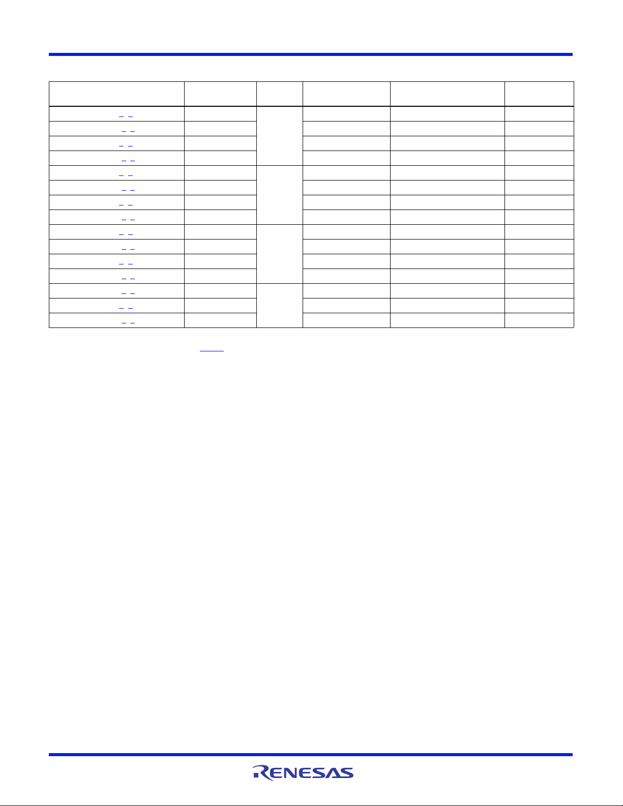
Ordering Information
PAR T
NUMBER
X9C102PZ (Notes 2
X9C102PIZ (Notes 2
X9C102SZ (Notes 1
X9C102SIZ (Notes 1
X9C103PZ (Notes 2
X9C103PIZ (Notes 2
X9C103SZ (Notes 1
X9C103SIZ (Notes 1
X9C503PZ (Notes 2
X9C503PIZ (Notes 2
X9C503SZ (Notes 1
X9C503SIZ (Notes 1
X9C104PIZ (Notes 2
X9C104SZ (Notes 1
X9C104SIZ (Notes 1
NOTES:
1. Add “T1” suffix for tape and reel. See TB347
2. These Pb-free plastic packaged products employ special Pb-free material sets, molding compounds/die attach materials, and 100% matte tin
plate plus anneal (e3 termination finish, which is RoHS compliant and compatible with both SnPb and Pb-free soldering operations). Pb-free
products are MSL classified at Pb-free peak reflow temperatures that meet or exceed the Pb-free requirements of IPC/JEDEC J STD-020.
3. Pb-free PDIPs can be used for through-hole wave solder processing only. They are not intended for use in Reflow solder processing applications.
, 3) X9C102P Z 1 0 to +70 8 Ld PDIP MDP0031
, 3) X9C102P ZI -40 to +85 8 Ld PDIP MDP0031
, 2) X9C102S Z 0 to +70 8 Ld SOIC M8.15E
, 2) X9C102S ZI -40 to +85 8 Ld SOIC M8.15E
, 3) X9C103P Z 10 0 to +70 8 Ld PDIP MDP0031
, 3) X9C103P ZI -40 to +85 8 Ld PDIP MDP0031
, 2) X9C103S Z 0 to +70 8 Ld SOIC M8.15
, 2) X9C103S ZI -40 to +85 8 Ld SOIC M8.15
, 3) X9C503P Z 50 0 to +70 8 Ld PDIP MDP0031
, 3) X9C503P ZI -40 to +85 8 Ld PDIP MDP0031
, 2) X9C503S Z 0 to +70 8 Ld SOIC M8.15E
, 2) X9C503S ZI -40 to +85 8 Ld SOIC M8.15E
, 3) X9C104P ZI 100 -40 to +85 8 Ld PDIP MDP0031
, 2) X9C104S Z 0 to +70 8 Ld SOIC M8.15E
, 2) X9C104S ZI -40 to +85 8 Ld SOIC M8.15E
PART
MARKING
for details about reel specifications.
R
TOTAL
(k)
TEMP RANGE
(°C)
PACKAGE
(RoHS Compliant)
PACKAGE
DWG. #
FN8222 Rev 4.00 Page 2 of 12
Jan 11, 2019
Page 3

X9C102, X9C103, X9C104, X9C503
Pin Descriptions
PIN
NUMBER PIN NAME DESCRIPTION
1INC
2U/D
3V
4V
5V
6R
H/RH
SS
W/RW
L/VL
7CS
8V
CC
INCREMENT The INC input is negative-edge triggered. Toggling INC will move the wiper and either increment or
decrement the counter in the direction indicated by the logic level on the U/D
UP/DOWN The U/D input controls the direction of the wiper movement and whether the counter is incremented or
decremented.
VH/RH The high (VH/RH) terminals of the X9C102, X9C103, X9C104, X9C503 are equivalent to the fixed terminals of
a mechanical potentiometer. The minimum voltage is -5V and the maximum is +5V. The terminology of V
references the relative position of the terminal in relation to wiper movement direction selected by the U/D input and
not the voltage potential on the terminal.
V
SS
VW/RW VW/RW is the wiper terminal and is equivalent to the movable terminal of a mechanical potentiometer. The
position of the wiper within the array is determined by the control inputs. The wiper terminal series resistance is typically
40.
RL/VL The low (VL/RL) terminals of the X9C102, X9C103, X9C104, X9C503 are equivalent to the fixed terminals of a
mechanical potentiometer. The minimum voltage is -5V and the maximum is +5V. The terminology of V
references the relative position of the terminal in relation to wiper movement direction selected by the U/D
not the voltage potential on the terminal.
CS The device is selected when the CS input is LOW. The current counter value is stored in non-volatile memory when
CS
is returned HIGH while the INC input is also HIGH. After the store operation is complete the X9C102, X9C103,
X9C104, X9C503 device will be placed in the low power standby mode until the device is selected once again.
V
CC
input.
H/RH
H/RH
and VL/R
and VL/RL
input and
L
FN8222 Rev 4.00 Page 3 of 12
Jan 11, 2019
Page 4

X9C102, X9C103, X9C104, X9C503
Absolute Maximum Ratings Thermal Information
Voltage on CS, INC, U/D and VCC with Respect to VSS . -1V to +7V
Voltage on V
V = |V
H/RH
X9C102 . . . . . . . . . . . . . . . . . . . . . . . . . . . . . . . . . . . . . . . . . . .4V
and VL/RL Referenced to VSS. . . . . . . -8V to +8V
H/RH
- VL/RL|
X9C103, X9C104, and X9C503 . . . . . . . . . . . . . . . . . . . . . . . .10V
I
(10s) . . . . . . . . . . . . . . . . . . . . . . . . . . . . . . . . . . . . . . . . . .8.8mA
W
Power Rating
X9C102 . . . . . . . . . . . . . . . . . . . . . . . . . . . . . . . . . . . . . . . .16mW
X9C103 X0C104, and X9C503 . . . . . . . . . . . . . . . . . . . . . .10mW
CAUTION: Do not operate at or near the maximum ratings listed for extended periods of time. Exposure to such conditions may adversely impact product reliability and
result in failures not covered by warranty.
Temperature Under Bias . . . . . . . . . . . . . . . . . . . . .-65°C to +135°C
Storage Temperature . . . . . . . . . . . . . . . . . . . . . . . .-65°C to +150°C
Pb-Free Reflow Profile. . . . . . . . . . . . . . . . . . . . . . . . . . . . . . TB493
*Pb-free PDIPs can be used for through-hole wave solder
processing only. They are not intended for use in Reflow solder
processing applications.
Recommended Operating Conditions
Commercial Temperature Range . . . . . . . . . . . . . . . . . 0°C to +70°C
Industrial Temperature Range . . . . . . . . . . . . . . . . . . -40°C to +85°C
Supply Voltage Range (V
) . . . . . . . . . . . . . . . . . . . . . . . 5V ±10%
CC
Electrical Specifications Over recommended operating conditions unless otherwise stated.
LIMITS
TYP
SYMBOL PARAMETER TEST CONDITIONS
POTENTIOMETER CHARACTERISTICS
R
V
V
TOTAL
VH/RH
VL/RL
I
W
R
W
End-to-End Resistance Variation -20 +20 %
VH Terminal Voltage -5 +5 V
VL Terminal Voltage -5 +5 V
Wiper Current -4.4 4.4 mA
Wiper Resistance Wiper Current = ±1mA 40 100
Resistor Noise (Note 8) Ref 1kHz -120 dBV
Charge Pump Noise (Note 8) @ 850kHz 20 mV
Resolution 1%
Absolute Linearity
Relative Linearity (Note 5) V
R
Temperature Coefficient X9C103, X9C503, X9C104 ±300 (Note 8) ppm/°C
TOTAL
R
Temperature Coefficient X9C102 ±600 (Note 8) ppm/°C
TOTAL
(Note 4) V
W(n)(actual)
W(n + 1)(ACTUAL)
- V
W(n)(EXPECTED)
- [V
Ratiometric Temperature Coefficient ±20 ppm/°C
C
H/CL/CW
(Note 8)
Potentiometer Capacitances See “Circuit #3 SPICE Macro
Model” on page 5.
DC OPERATING CHARACTERISTICS
I
CC
I
SB
I
LI
V
IH
V
IL
C
IN
VCC Active Current CS = VIL, U/D = VIL or VIH and
INC
= 0.4V to 2.4V at Max t
Standby Supply Current CS = VCC - 0.3V, U/D and
INC
=VSS or VCC-0.3V
CS, INC, U/D Input Leakage Current VIN = VSS to V
CC
CS, INC, U/D input HIGH Voltage 2 V
CS, INC, U/D input LOW Voltage 0.8 V
CS, INC, U/D Input Capacitance (Note 8) VCC = 5V, VIN = VSS, TA= +25°C,
f = 1MHz
(Note 7) MAX
-1 +1 MI (Note 6)
] -0.2 +0.2 MI (Note 6)
W(n) + MI
10/10/25 pF
13mA
CYC
200 750 µA
±10 µA
10 pF
UNITMIN
RMS
FN8222 Rev 4.00 Page 4 of 12
Jan 11, 2019
Page 5

X9C102, X9C103, X9C104, X9C503
Test Circuit #1
TEST POINT
Vw/R
W
VR/R
H
VL/R
L
V
S
Test Circuit #2
FORCE
VL/R
L
VW/R
w
VH/R
H
TEST POINT
CURRENT
Circuit #3 SPICE Macro Model
C
W
R
TOTAL
R
L
R
H
C
L
R
W
10pF
C
L
10pF
25pF
Electrical Specifications Over recommended operating conditions unless otherwise stated. (Continued)
LIMITS
SYMBOL PARAMETER TEST CONDITIONS
AC OPERATION CHARACTERISTICS
t
t
t
IW
t
t
t
t
Cl
t
lD
t
DI
t
lL
t
lH
t
lC
CPH
CPH
CYC
CYC
R, tF
t
PU
(5)
CS to INC Setup 100 ns
INC HIGH to U/D Change 100 ns
U/D to INC Setup 2.9 µs
INC LOW Period 1 µs
INC HIGH Period 1 µs
INC Inactive to CS Inactive 1 µs
CS Deselect Time (STORE) 20 ms
CS Deselect Time (NO STORE) 100 ns
INC to V
Change 100 µs
W/RW
INC Cycle Time 2 µs
INC Input Rise and Fall Time 500 µs
Power-up to Wiper Stable (Note 8) 500 µs
V
Power-up Rate (Note 8) 0.2 50 V/ms
CC
NOTES:
4. Absolute linearity is utilized to determine actual wiper voltage vs expected voltage = [V
5. Relative linearity is a measure of the error in step size between taps = V
6. 1 MI = Minimum Increment = R
7. Typical values are for T
= +25°C and nominal supply voltage.
A
TOT
/99.
W(n + 1)
8. This parameter is not 100% tested.
W(n)(actual)
- [V
W(n) + MI
- V
W(n)(expected )
] = +0.2 MI.
(Note 7) MAX
] = ±1 MI Maximum.
TYP
UNITMIN
Endurance and Data Retention
Medium Endurance 100,000 Data changes per bit
Data Retention 100 years
AC Conditions of Test
Input Pulse Levels 0V to 3V
Input Rise and Fall Times 10ns
Input Reference Levels 1.5V
FN8222 Rev 4.00 Page 5 of 12
Jan 11, 2019
PARAMETER MIN UNIT
per register
Power-up and Down Requirements
At all times, voltages on the potentiometer pins must be less
than ±V
memory is not in effect until the V
value. The V
. The recall of the wiper position from non-volatile
CC
ramp rate specification is always in effect.
CC
supply reaches its final
CC
Page 6

X9C102, X9C103, X9C104, X9C503
CS
INC
U/D
V
W
t
CI
t
IL
t
IH
t
CYC
t
ID
t
DI
t
IW
MI
t
IC
t
CPH
t
F
t
R
10%
90% 90%
(NOTE)
NOTE: MI REFERS TO THE MINIMUM INCREMENTAL CHANGE IN THE V
W
OUTPUT DUE TO A CHANGE IN THE WIPER POSITION.
AC Timing Diagram
Pin Descriptions
RH/VH and RL/V
The high (VH/RH) and low (VL/RL) terminals of the ISLX9C102,
X9C103, X9C104, X9C503 are equivalent to the fixed
terminals of a mechanical potentiometer. The minimum voltage
is -5V and the maximum is +5V. The terminology of V
V
references the relative position of the terminal in relation
L/RL
to wiper movement direction selected by the U/D
the voltage potential on the terminal.
RW/V
W
VW/RW is the wiper terminal, and is equivalent to the movable
terminal of a mechanical potentiometer. The position of the
wiper within the array is determined by the control inputs. The
wiper terminal series resistance is typically 40.
Up/Down (U/D)
The U/D input controls the direction of the wiper movement
and whether the counter is incremented or decremented.
Increment (INC)
The INC input is negative-edge triggered. Toggling INC will
move the wiper and either increment or decrement the counter
in the direction indicated by the logic level on the U/D
Chip Select (CS)
The device is selected when the CS input is LOW. The current
counter value is stored in non-volatile memory when CS
returned HIGH while the INC
operation is complete the ISLX9C102, X9C103, X9C104,
X9C503 device will be placed in the low power standby mode
until the device is selected once again.
L
and
H/RH
input and not
input.
is
input is also HIGH. After the store
Principles of Operation
There are three sections of the X9C102, X9C103, ISL9C104
and ISL9C503: the input control, counter and decode section;
the non-volatile memory; and the resistor array. The input control
section operates just like an up/down counter. The output of this
counter is decoded to turn on a single electronic switch
connecting a point on the resistor array to the wiper output.
Under the proper conditions, the contents of the counter can be
stored in non-volatile memory and retained for future use. The
resistor array is comprised of 99 individual resistors connected
in series. At either end of the array and between each resistor is
an electronic switch that transfers the potential at that point to
the wiper.
The wiper, when at either fixed terminal, acts like its
mechanical equivalent and does not move beyond the last
position. That is, the counter does not wrap around when
clocked to either extreme.
The electronic switches on the device operate in a
“make-before-break” mode when the wiper changes tap
positions. If the wiper is moved several positions, multiple taps
are connected to the wiper for t
R
value for the device can temporarily be reduced by a
TOTAL
significant amount if the wiper is moved several positions.
When the device is powered-down, the last wiper position
stored will be maintained in the non-volatile memory. When
power is restored, the contents of the memory are recalled and
the wiper is reset to the value last stored.
The internal charge pump allows a wide range of voltages
(from -5V to 5V) applied to XDCP terminals yet given a
convenience of single power supply. The typical charge pump
noise of 20mV at 850kHz should be taken in consideration
when designing an application circuit.
(INC to VW/RW change). The
IW
FN8222 Rev 4.00 Page 6 of 12
Jan 11, 2019
Page 7

X9C102, X9C103, X9C104, X9C503
WAVEFORM INPUTS OUTPUTS
Must be
steady
Will be
steady
May change
from Low to
High
Will change
from Low to
High
May change
from High to
Low
Will change
from High to
Low
Don’t Care:
Changes
Allowed
Changing:
State Not
Known
N/A Center Line
is High
Impedance
Instructions and Programming
The INC, U/D and CS inputs control the movement of the wiper
along the resistor array. With CS
and enabled to respond to the U/D
LOW transitions on INC
on the state of the U/D
will increment or decrement (depending
input) a 7-bit counter. The output of this
counter is decoded to select one of one-hundred wiper positions
along the resistive array.
The value of the counter is stored in non-volatile memory
whenever CS
transitions HIGH while the INC input is also
HIGH.
The system may select the X9Cxxx, move the wiper and
deselect the device without having to store the latest wiper
position in non-volatile memory. After the wiper movement is
performed as previously described and once the new position
is reached, the system must keep INC
HIGH. The new wiper position will be maintained until changed
by the system or until a power-down/up cycle recalled the
previously stored data.
This procedure allows the system to always power-up to a preset value stored in non-volatile memory; then during system
operation, minor adjustments could be made. The adjustments
might be based on user preference, i.e.: system parameter
changes due to temperature drift, etc.
set LOW, the device is selected
and INC inputs. HIGH to
LOW while taking CS
Mode Selection
CS INC U/D MODE
L H Wiper Up
L L Wiper Down
H X Store Wiper Position
H X X Standby Current
L X No Store, Return to Standby
L H Wiper Up (not recommended)
L L Wiper Down (not recommended)
Symbol Table
The state of U/D
may be changed while CS remains LOW. This
allows the host system to enable the device and then move the
wiper up and down until the proper trim is attained.
Performance Characteristics
Contact the factory for more information.
Applications Information
Electronic digitally controlled (XCDP) potentiometers provide
three powerful application advantages:
1. The variability and reliability of a solid-state potentiometer.
2. The flexibility of computer-based digital controls.
3. The retentivity of non-volatile memory used for the storage
of multiple potentiometer settings or data.
FN8222 Rev 4.00 Page 7 of 12
Jan 11, 2019
Page 8

X9C102, X9C103, X9C104, X9C503
V
R
V
R
I
THREE TERMINAL POTENTIOMETER;
VARIABLE VOLTAGE DIVIDER
TWO TERMINAL VARIABLE RESISTOR;
VARIABLE CURRENT
VH/R
H
VL/R
L
VW/R
W
CASCADING TECHNIQUESBUFFERED REFERENCE VOLTAGE
–
+
+5V
R
1
+V
-5V
V
W
V
REF
V
OUT
OP-07
VW/R
W
VW/R
W
+V
+V +V
X
(a) (b)
V
OUT
= VW/R
W
NONINVERTING AMPLIFIER
V
O
= (1+ R2/R1)V
S
VOLTAGE REGULATOR
R
1
R
2
I
adj
VO (REG) = 1.25V (1+R2/R1)+I
adj R2
VO (REG)V
IN
317
OFFSET VOLTAGE ADJUSTMENT
+
–
V
S
V
O
R
2
R
1
100k
10k10k
10k
-12V+12V
TL072
COMPARATOR WITH HYSTERESIS
V
UL
= {R1/(R1 + R2)} VO(MAX)
V
LL
= {R1/(R1 + R2)} VO(MIN)
+
–
V
S
V
O
R
2
R
1
LM308A
+5V
-5V
+
–
V
S
V
O
R
2
R
1
}
}
LT311A
(FOR ADDITIONAL CIRCUITS SEE AN1145)
Basic Configurations of Electronic Potentiometers
Basic Circuits
Revision History
Rev. Date Description
4.00 Jan 11, 2019 Updated Ordering Information table to remove Obsolete and Retired parts.
FN8222 Rev 4.00 Page 8 of 12
Jan 11, 2019
Added Revision History.
Updated PODs for X9C102, X9C104, and X9C503 SOICs from: MDP0027 to: M8.15E and X9C103 SOIC from:
MDP0027 to: M8.15, to include the Land Pattern design and convert dimensions from table to graphics.
Updated Intersil disclaimer to Renesas disclaimer.
Page 9

X9C102, X9C103, X9C104, X9C503
DETAIL "A"
TOP VIEW
INDEX
AREA
123
-C-
SEATING PLANE
x 45°
NOTES:
9. Dimensioning and tolerancing per ANSI Y14.5M-1994.
10. Package length does not include mold flash, protrusions or gate burrs.
Mold flash, protrusion and gate burrs shall not exceed 0.15mm (0.006
inch) per side.
11. Package width does not include interlead flash or protrusions. Interlead
flash and protrusions shall not exceed 0.25mm (0.010 inch) per side.
12. The chamfer on the body is optional. If it is not present, a visual index
feature must be located within the crosshatched area.
13. Terminal numbers are shown for reference only.
14. The lead width as measured 0.36mm (0.014 inch) or greater above the
seating plane, shall not exceed a maximum value of 0.61mm (0.024 inch).
15. Controlling dimension: MILLIMETER. Converted inch dimensions are not
necessarily exact.
16. This outline conforms to JEDEC publication MS-012-AA ISSUE C.
SIDE VIEW “A
SIDE VIEW “B”
1.27 (0.050)
6.20 (0.244)
5.80 (0.228)
4.00 (0.157)
3.80 (0.150)
0.50 (0.20)
0.25 (0.01)
5.00 (0.197)
4.80 (0.189)
1.75 (0.069)
1.35 (0.053)
0.25(0.010)
0.10(0.004)
0.51(0.020)
0.33(0.013)
8°
0°
0.25 (0.010)
0.19 (0.008)
1.27 (0.050)
0.40 (0.016)
1.27 (0.050)
5.20(0.205)
1
2
3
4
5
6
7
8
TYPICAL RECOMMENDED LAND PATTERN
2.20 (0.087)
0.60 (0.023)
Package Outline Drawings
M8.15
8 LEAD NARROW BODY SMALL OUTLINE PLASTIC PACKAGE
Rev 4, 1/12
For the most recent package outline drawing, see M8.15.
FN8222 Rev 4.00 Page 9 of 12
Jan 11, 2019
Page 10

X9C102, X9C103, X9C104, X9C503
Unless otherwise specified, tolerance : Decimal ± 0.05
The pin #1 identifier may be either a mold or mark feature.
Interlead flash or protrusions shall not exceed 0.25mm per side.
Dimension does not include interlead flash or protrusions.
Dimensions in ( ) for Reference Only.
Dimensioning and tolerancing conform to AMSE Y14.5m-1994.
3.
5.
4.
2.
Dimensions are in millimeters.1.
NOTES:
DETAIL "A"
SIDE VIEW “A
TYPICAL RECOMMENDED LAND PATTERN
TOP VIEW
A
B
4
4
0.25 AMC B
C
0.10 C
5
ID MARK
PIN NO.1
(0.35) x 45°
SEATING PLANE
GAUGE PLANE
0.25
(5.40)
(1.50)
4.90 ± 0.10
3.90 ± 0.10
1.27
0.43 ± 0.076
0.63 ±0.23
4° ± 4°
DETAIL "A"
0.22 ± 0.03
0.175 ± 0.075
1.45 ± 0.1
1.75 MAX
(1.27)
(0.60)
6.0 ± 0.20
Reference to JEDEC MS-012.
6.
SIDE VIEW “B”
M8.15E
8 LEAD NARROW BODY SMALL OUTLINE PLASTIC PACKAGE
Rev 0, 08/09
For the most recent package outline drawing, see M8.15E.
FN8222 Rev 4.00 Page 10 of 12
Jan 11, 2019
Page 11

X9C102, X9C103, X9C104, X9C503
D
L
A
e
b
A1
NOTE 5
A2
SEATING
PLANE
L
N
PIN #1
INDEX
E1
12 N/2
b2
E
eB
eA
c
Plastic Dual-In-Line Packages (PDIP)
For the most recent package outline drawing, see MDP0031.
MDP0031
PLASTIC DUAL-IN-LINE PACKAGE
INCHES
SYMBOL
A 0.210 0.210 0.210 0.210 0.210 MAX
A1 0.015 0.015 0.015 0.015 0.015 MIN
A2 0.130 0.130 0.130 0.130 0.130 ±0.005
b 0.018 0.018 0.018 0.018 0.018 ±0.002
b2 0.060 0.060 0.060 0.060 0.060 +0.010/-0.015
c 0.010 0.010 0.010 0.010 0.010 +0.004/-0.002
D 0.375 0.750 0.750 0.890 1.020 ±0.010 1
E 0.310 0.310 0.310 0.310 0.310 +0.015/-0.010
E1 0.250 0.250 0.250 0.250 0.250 ±0.005 2
e 0.100 0.100 0.100 0.100 0.100 Basic
eA 0.300 0.300 0.300 0.300 0.300 Basic
eB 0.345 0.345 0.345 0.345 0.345 ±0.025
L 0.125 0.125 0.125 0.125 0.125 ±0.010
N 8 14 16 18 20 Reference
NOTES:
17. Plastic or metal protrusions of 0.010” maximum per side are not included.
18. Plastic interlead protrusions of 0.010” maximum per side are not included.
19. Dimensions E and eA are measured with the leads constrained perpendicular to the seating plane.
20. Dimension eB is measured with the lead tips unconstrained.
21. 8 and 16 lead packages have half end-leads as shown.
TOLERANCE NOTESPDIP8 PDIP14 PDIP16 PDIP18 PDIP20
Rev. C 2/07
FN8222 Rev 4.00 Page 11 of 12
Jan 11, 2019
Page 12

http://www.renesas.com
Refer to "http://www.renesas.com/" for the latest and detailed information.
Renesas Electronics Corporation
TOYOSU FORESIA, 3-2-24 Toyosu, Koto-ku, Tokyo 135-0061, Japan
Renesas Electronics America Inc.
1001 Murphy Ranch Road, Milpitas, CA 95035, U.S.A.
Tel: +1-408-432-8888, Fax: +1-408-434-5351
Renesas Electronics Canada Limited
9251 Yonge Street, Suite 8309 Richmond Hill, Ontario Canada L4C 9T3
Tel: +1-905-237-2004
Renesas Electronics Europe Limited
Dukes Meadow, Millboard Road, Bourne End, Buckinghamshire, SL8 5FH, U.K
Tel: +44-1628-651-700
Renesas Electronics Europe GmbH
Arcadiastrasse 10, 40472 Düsseldorf, Germany
Tel: +49-211-6503-0, Fax: +49-211-6503-1327
Renesas Electronics (China) Co., Ltd.
Room 1709 Quantum Plaza, No.27 ZhichunLu, Haidian District, Beijing, 100191 P. R. China
Tel: +86-10-8235-1155, Fax: +86-10-8235-7679
Renesas Electronics (Shanghai) Co., Ltd.
Unit 301, Tower A, Central Towers, 555 Langao Road, Putuo District, Shanghai, 200333 P. R. China
Tel: +86-21-2226-0888, Fax: +86-21-2226-0999
Renesas Electronics Hong Kong Limited
Unit 1601-1611, 16/F., Tower 2, Grand Century Place, 193 Prince Edward Road West, Mongkok, Kowloon, Hong Kong
Tel: +852-2265-6688, Fax: +852 2886-9022
Renesas Electronics Taiwan Co., Ltd.
13F, No. 363, Fu Shing North Road, Taipei 10543, Taiwan
Tel: +886-2-8175-9600, Fax: +886 2-8175-9670
Renesas Electronics Singapore Pte. Ltd.
80 Bendemeer Road, Unit #06-02 Hyflux Innovation Centre, Singapore 339949
Tel: +65-6213-0200, Fax: +65-6213-0300
Renesas Electronics Malaysia Sdn.Bhd.
Unit 1207, Block B, Menara Amcorp, Amcorp Trade Centre, No. 18, Jln Persiaran Barat, 46050 Petaling Jaya, Selangor Darul Ehsan, Malaysia
Tel: +60-3-7955-9390, Fax: +60-3-7955-9510
Renesas Electronics India Pvt. Ltd.
No.777C, 100 Feet Road, HAL 2nd Stage, Indiranagar, Bangalore 560 038, India
Tel: +91-80-67208700, Fax: +91-80-67208777
Renesas Electronics Korea Co., Ltd.
17F, KAMCO Yangjae Tower, 262, Gangnam-daero, Gangnam-gu, Seoul, 06265 Korea
Tel: +82-2-558-3737, Fax: +82-2-558-5338
SALES OFFICES
© 2018 Renesas Electronics Corporation. All rights reserved.
Colophon 7.2
(Rev.4.0-1 November 2017)
Notice
1. Descriptions of circuits, software and other related information in this document are provided only to illustrate the operation of semiconductor products and application examples. You are fully responsible for
the incorporation or any other use of the circuits, software, and information in the design of your product or system. Renesas Electronics disclaims any and all liability for any losses and damages incurred by
you or third parties arising from the use of these circuits, software, or information.
2. Renesas Electronics hereby expressly disclaims any warranties against and liability for infringement or any other claims involving patents, copyrights, or other intellectual property rights of third parties, by or
arising from the use of Renesas Electronics products or technical information described in this document, including but not limited to, the product data, drawings, charts, programs, algorithms, and application
examples.
3. No license, express, implied or otherwise, is granted hereby under any patents, copyrights or other intellectual property rights of Renesas Electronics or others.
4. You shall not alter, modify, copy, or reverse engineer any Renesas Electronics product, whether in whole or in part. Renesas Electronics disclaims any and all liability for any losses or damages incurred by
you or third parties arising from such alteration, modification, copying or reverse engineering.
5. Renesas Electronics products are classified according to the following two quality grades: “Standard” and “High Quality”. The intended applications for each Renesas Electronics product depends on the
product’s quality grade, as indicated below.
"Standard": Computers; office equipment; communications equipment; test and measurement equipment; audio and visual equipment; home electronic appliances; machine tools; personal electronic
equipment; industrial robots; etc.
"High Quality": Transportation equipment (automobiles, trains, ships, etc.); traffic control (traffic lights); large-scale communication equipment; key financial terminal systems; safety control equipment; etc.
Unless expressly designated as a high reliability product or a product for harsh environments in a Renesas Electronics data sheet or other Renesas Electronics document, Renesas Electronics products are
not intended or authorized for use in products or systems that may pose a direct threat to human life or bodily injury (artificial life support devices or systems; surgical implantations; etc.), or may cause
serious property damage (space system; undersea repeaters; nuclear power control systems; aircraft control systems; key plant systems; military equipment; etc.). Renesas Electronics disclaims any and all
liability for any damages or losses incurred by you or any third parties arising from the use of any Renesas Electronics product that is inconsistent with any Renesas Electronics data sheet, user’s manual or
other Renesas Electronics document.
6. When using Renesas Electronics products, refer to the latest product information (data sheets, user’s manuals, application notes, “General Notes for Handling and Using Semiconductor Devices” in the
reliability handbook, etc.), and ensure that usage conditions are within the ranges specified by Renesas Electronics with respect to maximum ratings, operating power supply voltage range, heat dissipation
characteristics, installation, etc. Renesas Electronics disclaims any and all liability for any malfunctions, failure or accident arising out of the use of Renesas Electronics products outside of such specified
ranges.
7. Although Renesas Electronics endeavors to improve the quality and reliability of Renesas Electronics products, semiconductor products have specific characteristics, such as the occurrence of failure at a
certain rate and malfunctions under certain use conditions. Unless designated as a high reliability product or a product for harsh environments in a Renesas Electronics data sheet or other Renesas
Electronics document, Renesas Electronics products are not subject to radiation resistance design. You are responsible for implementing safety measures to guard against the possibility of bodily injury, injury
or damage caused by fire, and/or danger to the public in the event of a failure or malfunction of Renesas Electronics products, such as safety design for hardware and software, including but not limited to
redundancy, fire control and malfunction prevention, appropriate treatment for aging degradation or any other appropriate measures. Because the evaluation of microcomputer software alone is very difficult
and impractical, you are responsible for evaluating the safety of the final products or systems manufactured by you.
8. Please contact a Renesas Electronics sales office for details as to environmental matters such as the environmental compatibility of each Renesas Electronics product. You are responsible for carefully and
sufficiently investigating applicable laws and regulations that regulate the inclusion or use of controlled substances, including without limitation, the EU RoHS Directive, and using Renesas Electronics
products in compliance with all these applicable laws and regulations. Renesas Electronics disclaims any and all liability for damages or losses occurring as a result of your noncompliance with applicable
laws and regulations.
9. Renesas Electronics products and technologies shall not be used for or incorporated into any products or systems whose manufacture, use, or sale is prohibited under any applicable domestic or foreign laws
or regulations. You shall comply with any applicable export control laws and regulations promulgated and administered by the governments of any countries asserting jurisdiction over the parties or
transactions.
10. It is the responsibility of the buyer or distributor of Renesas Electronics products, or any other party who distributes, disposes of, or otherwise sells or transfers the product to a third party, to notify such third
party in advance of the contents and conditions set forth in this document.
11. This document shall not be reprinted, reproduced or duplicated in any form, in whole or in part, without prior written consent of Renesas Electronics.
12. Please contact a Renesas Electronics sales office if you have any questions regarding the information contained in this document or Renesas Electronics products.
(Note 1) “Renesas Electronics” as used in this document means Renesas Electronics Corporation and also includes its directly or indirectly controlled subsidiaries.
(Note 2) “Renesas Electronics product(s)” means any product developed or manufactured by or for Renesas Electronics.
All trademarks and registered trademarks are the property of their respective owners.
 Loading...