

Page 1
Date: Feb. 3, 2021
RENESAS TECHNICAL UPDATE
TOYOSU FORESIA, 3-2-24, Toyosu, Koto-ku, Tokyo 135-0061, Japan
Renesas Electronics Corporation
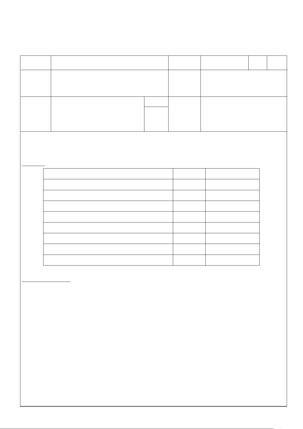
Product
Category
MPU/MCU
Document
No.
Rev.
1.00
Title
Correction for Incorrect Description Notice
RL78/L13 Descriptions in the User’s Manual: Hardware
Rev. 2.10 Changed
Information
Category
Technical Notification
Applicable
Product
RL78/L13 Group
Lot No.
Reference
Document
RL78/L13 User’s Manual: Hardware
Rev. 2.10
R01UH0382EJ0210 (Aug 12,2016)
All lots
Applicable Item
Applicable
Page
Contents
5.4.4 Low-speed on-chip oscillator
Page 169
Incorrect descriptions
revised
7.9.2 Cautions when using the counter restart trigger
Page 386
Incorrect descriptions
revised
11.1 Functions of Watchdog Timer
Page 433
Incorrect descriptions
revised
11.4.4 Setting watchdog timer interval interrupt
Page 439
Incorrect descriptions
revised
14.3.14 Serial standby control register m (SSCm)
Page 526
Incorrect descriptions
revised
16.6 Setting the LCD Controller/Driver
Page 770
Incorrect descriptions
revised
22.2 States of Operation During Reset Periods
Page 891
Incorrect descriptions
revised
27.2 Format of User Option Byte
Page 939
Incorrect descriptions
revised
TN-RL*-A0098A/E
This document describes misstatements found in the RL78/L13 User’s Manual: Hardware Rev. 2.10 (R01UH0382EJ0210).
Corrections
Document Improvement
The above corrections will be made for the next revision of the User’s Manual: Hardware.
© 2021 Renesas Electronics Corporation. All rights reserved.
Page 1 of 7
Page 2
RENESAS TECHNICAL UPDATE TN-RL*-A0098A/E
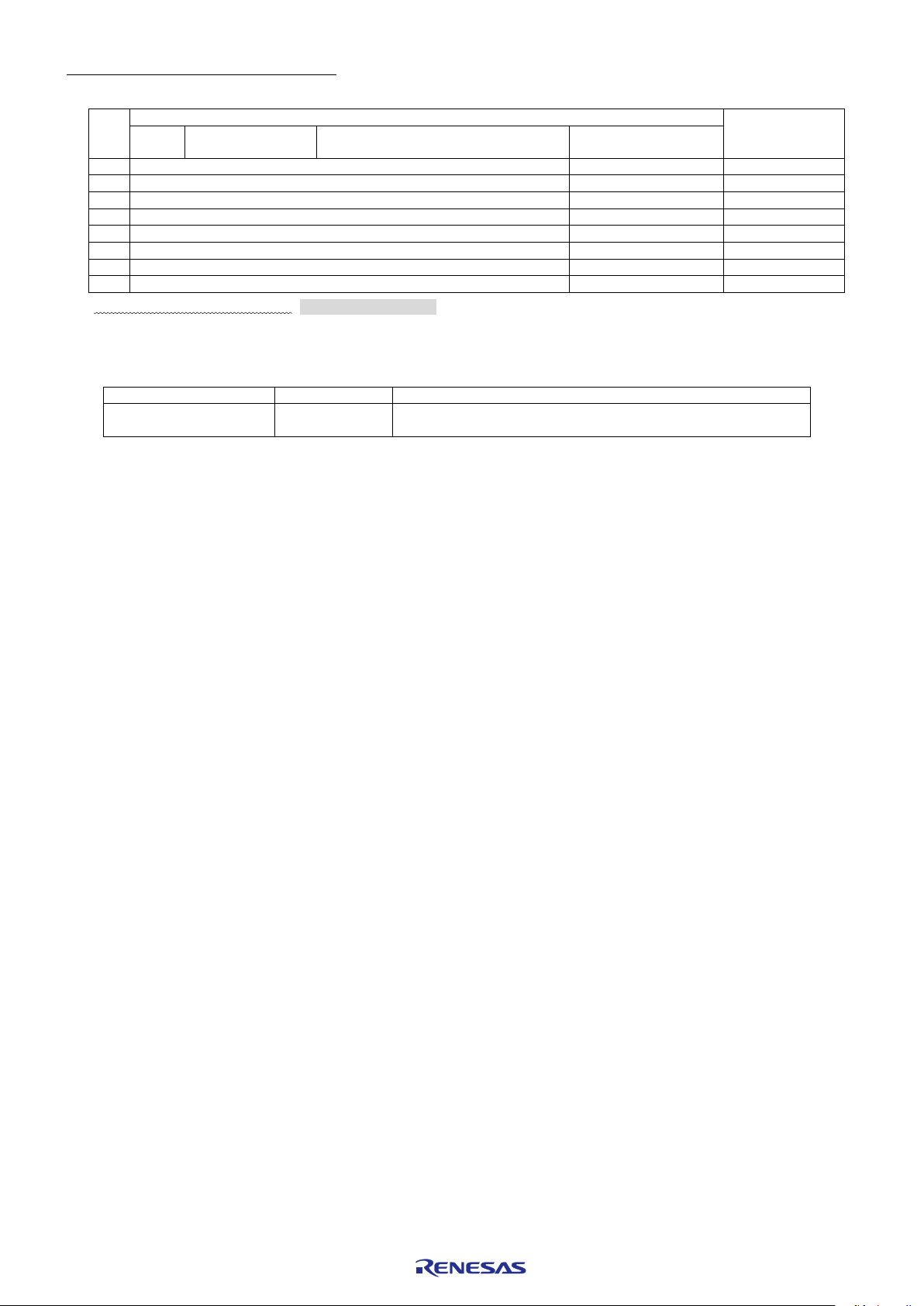
No.
Corrections and Applicable Items
Pages in this
document for
corrections
Document No.
English
R01UH0409EJ0210
1
5.4.4 Low-speed on-chip oscillator
Page 169
Page 3
2
7.9.2 Cautions when using the counter restart trigger
Page 386
Page 4
3
11.1 Functions of Watchdog Timer
Page 433
Page 4
4
11.4.4 Setting watchdog timer interval interrupt
Page 439
Page 5
5
14.3.14 Serial standby control register m (SSCm)
Page 526
Page 5
6
16.6 Setting the LCD Controller/Driver
Page 770
Page 6
7
22.2 States of Operation During Reset Periods
Page 891
Page 6
8
27.2 Format of User Option Byte
Page 939
Page 7
Document Number
Issue Date
Description
First edition issued
Corrections No.1 to No.8 revised (this document)
Corrections in the User’s Manual: Hardware
Incorrect: Bold with underline; Correct: Gray hatched
Revision History
RL78/L1C Correction for incorrect description notice
TN-RL*-A0098A/E Feb. 3, 2021
Date: Feb. 3, 2021
© 2021 Renesas Electronics Corporation. All rights reserved.
Page 2 of 7
Page 3
RENESAS TECHNICAL UPDATE TN-RL*-A0098A/E Date: Feb. 3, 2021
1. 5.4.4 Low-speed on-chip oscillator (p.169)
Incorrect:
A low-speed on-chip oscillator is incorporated in the RL78/L13.
The low-speed on-chip oscillator clock is used only as the clock for the
watchdog timer, real-time clock 2, 12-bit interval timer, and the LCD
controller/driver. The low-speed on-chip oscillator clock cannot be used as
the CPU clock.
This clock operates when either bit 4 (WDTON) of the option byte
(000C0H) or bit 4 (WUTMMCK0) of the subsystem clock supply mode
control register (OSMC), or both, are set to 1.
As long as the watchdog timer is not operating and WUTMMCK0 is not
zero, the low-speed on-chip oscillator continues oscillating. Note that
only when the watchdog timer is operating and the WUTMMCK0 bit is 0,
oscillation of the low-speed on-chip oscillator will stop while the
WDSTBYON bit is 0 and operation is in the HALT, STOP, or SNOOZE
mode. The low-speed on-chip oscillator clock does not stop even if a
program loop that stops the system occurs while the watchdog timer is
operating.
Correct:
A low-speed on-chip oscillator is incorporated in the RL78/L13.
The low-speed on-chip oscillator clock is used only as the clock for the
watchdog timer, real-time clock 2, 12-bit interval timer, and the LCD
controller/driver. The low-speed on-chip oscillator clock cannot be used as
the CPU clock.
The low-speed on-chip oscillator runs while the watchdog timer is operating or
when the setting of bit 4 (WUTMMCK0) in the subsystem clock supply mode
control register (OSMC) is 1.
The low-speed on-chip oscillator is stopped when the watchdog timer is
stopped and WUTMMCK0 is set to 0.
© 2021 Renesas Electronics Corporation. All rights reserved.
Page 3 of 7
Page 4

RENESAS TECHNICAL UPDATE TN-RL*-A0098A/E Date: Feb. 3, 2021
2. 7.9.2 Cautions when using the counter restart trigger (p.386)
Incorrect:
(1) Using external interrupts (INTP0 to INTP7)
INTP0 to INTP7, which are used as counter restart trigger sources, are not
affected by the settings of the external interrupt rising edge enable register
(EGP0) or external interrupt falling edge enable register (EGN0). Only the
rising edge is valid.
3. 11.1 Functions of Watchdog Timer (p.433)
Incorrect:
(omitted)
When 75% + 1/2/fIL of the overflow time is reached, an interval interrupt
can be generated.
Correct:
(1) Using external interrupts (INTP0 to INTP7)
INTP0 to INTP7, which are used as counter restart trigger sources, are not
affected by the settings of the external interrupt rising edge enable register
(EGP0) or external interrupt falling edge enable register (EGN0). Only the
rising edge is valid.
However, when using the PWM output function for IH control, the active edge
can be selected by 16-bit timer KB2 output control register 01 (TKBIOC01).
Correct:
(omitted)
When 75% of the overflow time + 1/2 fIL is reached, an interval interrupt
can be generated.
© 2021 Renesas Electronics Corporation. All rights reserved.
Page 4 of 7
Page 5

WDTINT
Use of Watchdog Timer Interval Interrupt
0
Interval interrupt is used.
1
Interval interrupt is generated when 75% + 1/2fIL of overflow
time is reached.
WDTINT
Use of Watchdog Timer Interval Interrupt
0
Interval interrupt is used.
1
Interval interrupt is generated when 75% of the overflow time + 1/2 fIL
is reached.
RENESAS TECHNICAL UPDATE TN-RL*-A0098A/E Date: Feb. 3, 2021
4. 11.4.4 Setting watchdog timer interval interrupt (p.439)
Incorrect:
Depending on the setting of bit 7 (WDTINT) of an option byte (000C0H), an
interval interrupt (INTWDTI) can be generated when 75% + 1/2fIL of the
overflow time is reached.
Table 11-5. Setting of Watchdog Timer Interval Interrupt
5. 14.3.14 Serial standby control register m (SSCm) (p.526)
Incorrect:
(omitted)
Caution The maximum transfer rate in the SNOOZE mode is as follows.
• When using CSI00: 1 Mbps
• When using UART0, UART2: 9600 bps
Correct:
Depending on the setting of bit 7 (WDTINT) of an option byte (000C0H), an
interval interrupt (INTWDTI) can be generated when 75% of the overflow time
+ 1/2 fIL is reached.
Table 11-5. Setting of Watchdog Timer Interval Interrupt
Correct:
(omitted)
Caution The maximum transfer rate in the SNOOZE mode is as follows.
• When using CSI00: 1 Mbps
• When using UART0, UART2: 4800 bps
© 2021 Renesas Electronics Corporation. All rights reserved.
Page 5 of 7
Page 6

Item
During Reset Period
System clock
(omitted)
Subsystem
clock
fXT
Operation possible
(the XT1 and XT2 pins are input port mode)
(omitted)
Item
During Reset Period
System clock
(omitted)
Subsystem
clock
fXT
Operation possible
(omitted)
START
(omitted)
(omitted)
Specify the LCD clock by using
the LCDC0 and MCDC registers.
START
(omitted)
(omitted)
Specify the LCD clock by using
the LCDC0 register.
RENESAS TECHNICAL UPDATE TN-RL*-A0098A/E Date: Feb. 3, 2021
6. 16.6 Setting the LCD Controller/Driver (p.770)
Incorrect:
(1) External resistance division method
Figure 16-17. External Resistance Division Method Setting Procedure
7. 22.2 States of Operation During Reset Periods (p.891)
Incorrect:
Table 22-1. Operation Statuses During Reset Period
Correct:
(1) External resistance division method
Figure 16-17. External Resistance Division Method Setting Procedure
Correct:
Table 22-1. Operation Statuses During Reset Period
© 2021 Renesas Electronics Corporation. All rights reserved.
Page 6 of 7
Page 7

WDTINT
Use of interval interrupt of watchdog timer
0
Interval interrupt is used.
1
Interval interrupt is generated when 75% + 1/2fIL of overflow
time is reached.
WDTINT
Use of interval interrupt of watchdog timer
0
Interval interrupt is used.
1
Interval interrupt is generated when 75% of the overflow time +
1/2 fIL is reached.
RENESAS TECHNICAL UPDATE TN-RL*-A0098A/E Date: Feb. 3, 2021
8. 27.2 Format of User Option Byte (p.939)
Incorrect:
Figure 27-1. Format of User Option Byte (000C0H/010C0H)
(omitted)
Corrected:
Figure 27-1. Format of User Option Byte (000C0H/010C0H)
(omitted)
© 2021 Renesas Electronics Corporation. All rights reserved.
Page 7 of 7
 Loading...