

Page 1
Application Note
Renesas RA Family
Using Trusted Firmware-M (TF-M) with FSP v2.0.3
Introduction
Arm® Platform Security Architecture (PSA) and PSA CertifiedTM are the next generation security specification
from Arm with certification support. Trusted Firmware-M (TF-M) is an open source collaboration which
implements the PSA specification for Arm Cortex
Trusted Firmware-M integrates with Renesas Flexible Software Package (FSP) to support PSA specification
implementation on the Renesas RA Family MCU groups. A working demonstration of firmware updates is
also included in this application project.
The software project provided in this application project is based on FSP 2.0.3 and EK-RA6M4, as per the
PSA Certified Level 2 FSP version. Subsequent FSP releases will continue to remain aligned with TF-M
updates.
For more in-depth knowledge on PSA and TF-M, user is encouraged to learn from the Arm PSA and TF-M
relevant links provided in the Reference section.
Required Resources
Development Tools and Software
• The e
• Renesas Flex Software Package (FSP) v2.0.3
• SEGGER J-link® USB driver
• Python 3.8 - https://www.python.org/downloads/
2
studio ISDE v2020-10
The above three software components: the FSP, J-Link USB drivers and e
downloadable platform installer available on the FSP webpage at renesas.com/ra/fsp
®
-M MCU groups. This application project introduces how
2
studio are bundled in a
Hardware
• EK-RA6M4, Evaluation Kit for RA6M4 MCU Group (http://www.renesas.com/ra/ek-ra6m4
• Workstation running Wind ows® 10; the Tera Term console, or similar application
• Two USB device cables (type-A male to micro-B male)
)
Prerequisites and Intended Audience
This application project assumes you have some experience with the Renesas e2 studio ISDE and FSP.
Before you perform the procedures in this application note, follow the FSP User’s Manual
Blinky project. Prior knowledge of PSA and TF-M is helpful. Prior knowledge on Python usage is helpful. The
intended audience are users who are interested in using TF-M with Renesas FSP package.
to build and run the
R11AN0493EU0100 Rev.1.00 Page 1 of 33
Mar.4.21
Page 2

Renesas RA Family Using Trusted Firmware-M (TF-M) with FSP v2.0.3
Contents
1. Arm® Platform Security Architecture and Trusted Firmware-M ................................................. 3
1.1 Why Arm Platform Security Architecture (PSA) ...................................................................................... 3
1.2 PSA CertifiedTM ........................................................................................................................................ 4
1.3 Trusted Firmware-M Proj ect .................................................................................................................... 5
1.3.1 Trusted Firmware-M as an Implementatio n of the PSA Specif icat io n ................................................... 5
1.3.2 History of TF-M/TF-A ............................................................................................................................. 6
1.3.3 TF-M Provides Secure World Services for the PSA RoT Use Case of TrustZone ............................... 6
TM
2. PSA Certified
2.1 Introduction to the PSA Isolation Level 2 ................................................................................................ 8
2.2 Testing of PSA Level 2 Implementati on .................................................................................................. 9
2.3 Certification of PSA CertifiedTM Level 2 with TF-M .................................................................................. 9
3. Using TFM V1.1 with FSP v2.0.3 ........................................................................................... 10
3.1 Using the TF-M Bootloader and Debug the Skeleton Projects ............................................................. 10
3.2 Debugging the Projects ......................................................................................................................... 13
Level 2 ........................................................................................................... 7
3.3 Making the Bootloader Immutable ......................................................................................................... 20
3.4 Device Lifecycle Management – Disabl ing the Deb ug and Fact or y Progra mm ing Interfaces .............. 22
3.5 Customizing a Renesas TF-M Implementation for an End Product ...................................................... 25
4. Example Project for Firmware Update ................................................................................... 27
4.1 Import and Download the Example Firmware Update Project .............................................................. 27
4.2 Running the Example Firmware Downloader Application ..................................................................... 27
5. References ............................................................................................................................ 31
6. Website and Support ............................................................................................................. 32
Revision History ............................................................................................................................ 33
Notice ............................................................................................................................................. 1
R11AN0493EU0100 Rev.1.00 Page 2 of 33
Mar.4.21
Page 3

Renesas RA Family Using Trusted Firmware-M (TF-M) with FSP v2.0.3
1. Arm® Platform Security Architecture and Trusted Firmware-M
1.1 Why Arm Platform Security Architecture (PSA)
Arm Platform Security Architecture (PSA) offers a framework for securing connected devices with a matching
evaluation scheme to check that security has been implemented correctly. Following are some PSA features
that a customer can benefit from for their security design.
• Build on a Common Foundation
Arm PSA offers a holistic set of MCU and firmware architectural specifications to guide customer
design and ens ures IoT secur ity c ommon foundation. Arm PSA ensures your device security is
based on a common foundation, supported by the Arm ecosystem with a complete set of specifications
guiding customers through the design and evaluation process. Below are the group of specifications.
1. PSA Security Model [PSA-SM] – Foundational trust models and patterns.
2. Factory Initialization [PSA-FI] – Requirements for initial secure device pr ogra mming
and configuration (yet to be available at the time of release of this Application Project).
3. Trusted Base System Architecture [TBSA-M] – Hardware platform requirements.
4. Trusted Boot and Firmware Update [TBFU].
5. Firmware Framework [PSA-FF] – Firmware interface definition of a Secure Processing.
6. Environment (SPE) for constrained IoT platforms, including PSA Root of Trust APIs.
7. Developer APIs – Interfaces to security services for application developers.
These PSA specifications greatly simplify the process of evaluating IoT devices against security standards.
For more details of the PSA Trusted Based System Architecture and Firmware Framework specifications,
please visit the Arm P SA websites here:
https://developer.arm.com/architectures/security-architectures/platform-security-architecture
• Reduce Costs and Time
Arm PSA reduces cost and complexity of software development for ecosystem partners by facilitating re-use,
improving interoperability, and minimizing API fragmentation.
The PSA Functional APIs define the foundations on which security services are built, allowing devices to be
secure by design. These APIs provide a consistent developer experience for RTOS and software developers
ensuring interoperability across different hardware implementations of the Root of Trust.
PSA also reduces cost of security and complexity for SoC designers– by leveraging from the primitives
offered by the PSA.
• Increase Confidence
PSA Certified
of security, and to help developers and customers trust that they can achieve the level of security they need.
By working with leading test labs, PSA Certified provides multi-level assurance for devices, depending on the
security requirements established through analysis of threats for a specific use case. Certifying your device
with independent security testing provides trust in the deployment of IoT at scale, drastically increasing
customer confidence.
TM
enables IoT chipsets and devices to be tested in laboratory conditions, to evaluate their level
R11AN0493EU0100 Rev.1.00 Page 3 of 33
Mar.4.21
Page 4
Renesas RA Family Using Trusted Firmware-M (TF-M) with FSP v2.0.3
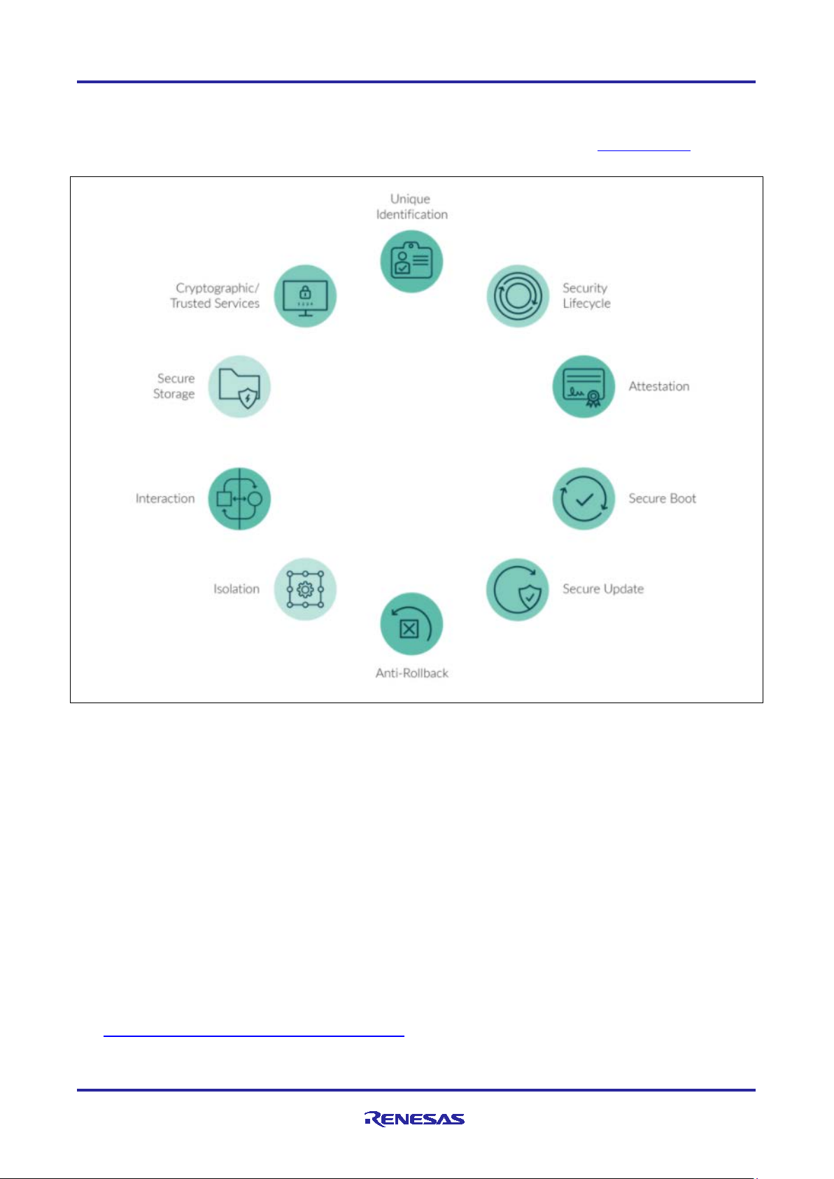
1.2 PSA CertifiedTM
PSA Certified program methodically uses IoT threat models, security goals and industry best practices to
provide free access to world-leading security expertise. The following image is from pascertifed.org which
shows some of the aspects PSA Certified test for in terms of system security.
Figure 1. Security Considerations
Standardized security considerations become more important with the increase in security breaches, system
complexity, as well as IoT device connectivity. PSA Certified is intended to give consumer device
manufacturers confidence that their products follow good security practices as being outlined by these
specifications.
There are three PSA Certification Levels.
• PSA Certified Level 1 is a concise set of methodically developed requirements that builds a foundation
of security for the IoT. This foundation is essential since most IoT attacks exploit the most basic
vulnerabilities. PSA Certified Level 1 aligns with key government requirement to ensure global
applicability and showcase security best practice. Renesas Synergy S5 Cortex-M4 MCU Groups, RA
Family RA6 Series Cortex-M4 and RA4/RA6 Cortex-CM33 MCU Groups are PSA Level 1 Certified.
• PSA Certified Level 2 provides a laboratory evaluation of a PSA Root of Trust (PSA-RoT) to provide
evidence that it can protect against scalable software attacks.
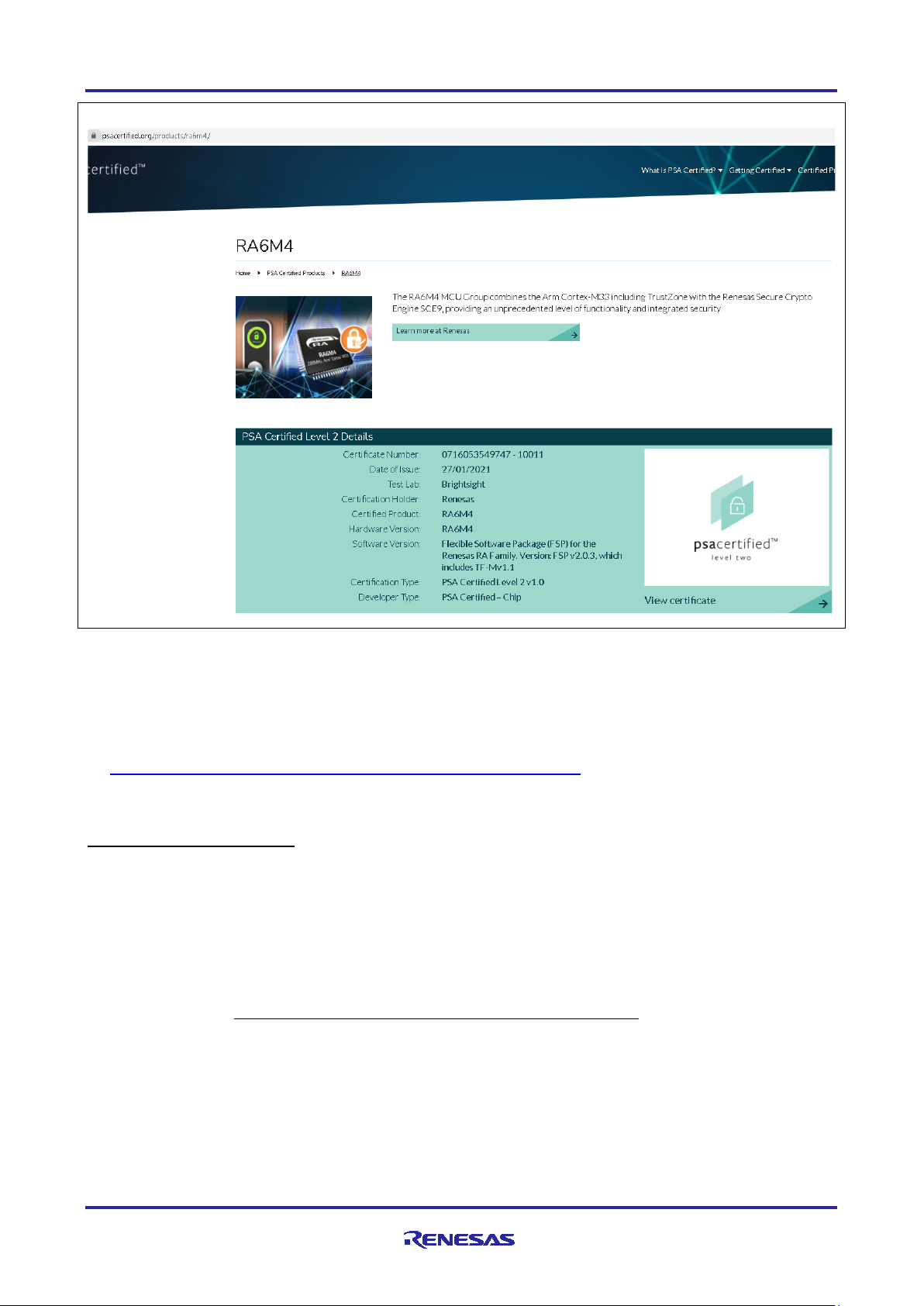
Renesas Cortex-M33 RA6M4 MCU Group with FSP v2.0.3 is PSA Certified Level 2.
PSA Functional API certification is a prerequisite of PSA Certified Level 2.
FSP 2.0.3 is PSA Functional API certified.
https://www.psacertified.org/products/ra6m4/
R11AN0493EU0100 Rev.1.00 Page 4 of 33
Mar.4.21
Page 5
Renesas RA Family Using Trusted Firmware-M (TF-M) with FSP v2.0.3
Figure 2. Renesas RA6M4 MCU Group with FSP 2.03 is PSA CertifiedTM Level 2
• PSA Certified Level 3 is currently under development, PSA Certified Level 3 will provide laboratory
assessment of IoT chips with substantial security capabilities.
For more details on the PSA Certified Governing Scheme, please visit
https://www.psacertified.org/getting-certified/silicon-vendor/overview/
.
1.3 Trusted Firmware-M Project
Trusted Firmware-M (TF-M) provides reference implementation of secure world software to implement
threat protections defined in common use cases. TF-M is based on the PSA Firmware Framework
specification and provides the reference implementation of the PSA Functional APIs.
1.3.1 Trusted Firmware-M as an Implementation of the PSA Specification
TF-M is the platform security architecture reference implementation aligning with PSA Certified guidelines,
enabling chips, Real Time Operating Systems and devices to become PSA Certified.
Trusted Firmware-M (TF-M) is being deve lop ed as an Open Sourc e pr ojec t under an Open Governance
Model, learn more at Trusted F irmw are: open sourc e S ecure wor ld s oftwar e
TF-M provides a Trusted Execution Environment (TEE) for Arm® v7-M and v8-M devices. For Arm v8-M
devices, TF-M leverages Arm TrustZone technology, and is the reference implementation of platform security
architecture aligning with PSA Certified guidelines.
.
Being a platinum board member, Renesas influences the mission and strategy of the TF-M project.
R11AN0493EU0100 Rev.1.00 Page 5 of 33
Mar.4.21
Page 6
Renesas RA Family Using Trusted Firmware-M (TF-M) with FSP v2.0.3
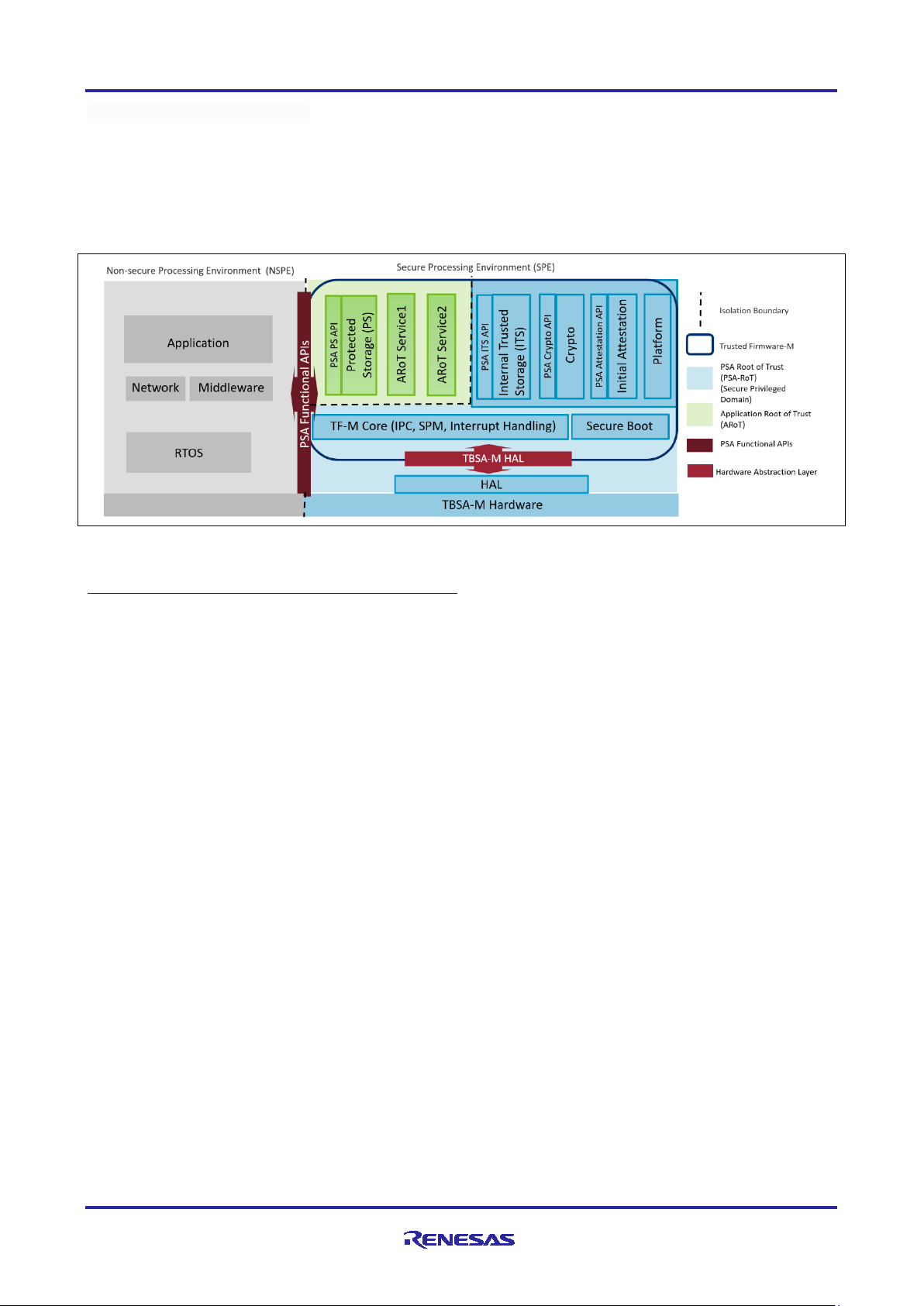
Trusted Firmware-M consists of:
• Secure Boot to authenticate integrity of Non-secur e Proc es sing Envir o nme nt (NSPE) and Secure
Processing Environment (SPE) images
• TF-M Core responsible for controlling the isolation, communication and execution within SPE and with
NSPE
• Cryptography, Internal Trusted Storage (ITS), Protected Storage (PS), and Attestation secure services.
Figure 3. TF-M Architecture
For future TF-M development road map, please refer to
https://developer.trustedfirmware.org/w/tf_m/planning/
.
1.3.2 History of TF-M/TF-A
Arm® Trusted Firmware provides a reference implementation of secure world software. Originally designed
and implemented for Cortex -A devices, Trusted Firmware-M forms the foundations of a Secure Processing
Environment (SPE) on Cortex-M devices. TF-M code is the preferred implementation of Arm specifications,
allowing quick and easy porting to modern chips and platforms.
1.3.3 TF-M Provides Secure World Services for the PSA RoT Use Case of TrustZone
As shown in Figure 3, the PSA RoT includes the following elements:
• MCU hardware level Immutable Unique Keys (reflected in the TBSA-M Hardware block)
• TF-M Secure Partition Manager, IPC and Interru pt Handling
• Secure Boot
• PSA ITS API, Crypto API and Attestation API
The secure world services provide PSA RoT use cases for the applications.
R11AN0493EU0100 Rev.1.00 Page 6 of 33
Mar.4.21
Page 7
Renesas RA Family Using Trusted Firmware-M (TF-M) with FSP v2.0.3
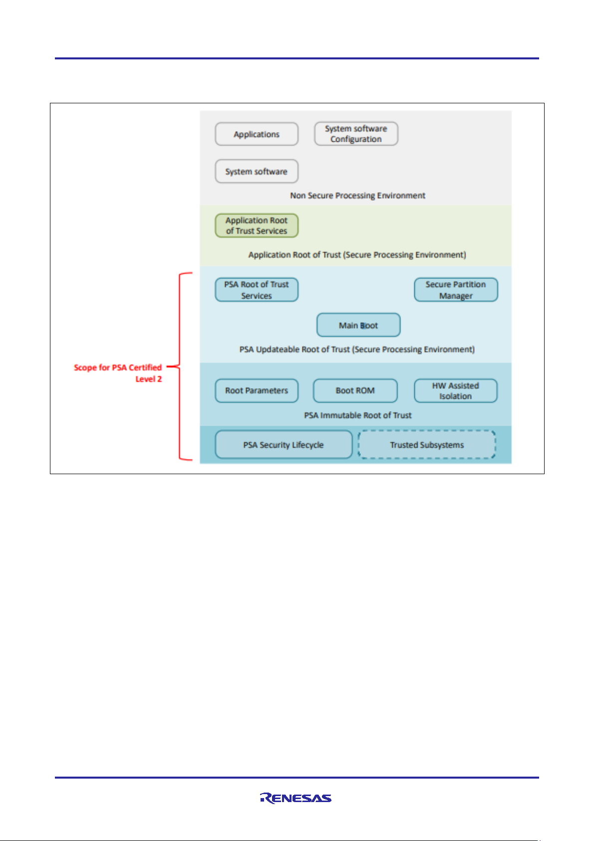
2. PSA CertifiedTM Level 2
The following architecture diagram shows the scope of PSA Certified Level 2 evaluation.
Figure 4. Scope of PSA Certified Level 2
R11AN0493EU0100 Rev.1.00 Page 7 of 33
Mar.4.21
Page 8
Renesas RA Family Using Trusted Firmware-M (TF-M) with FSP v2.0.3
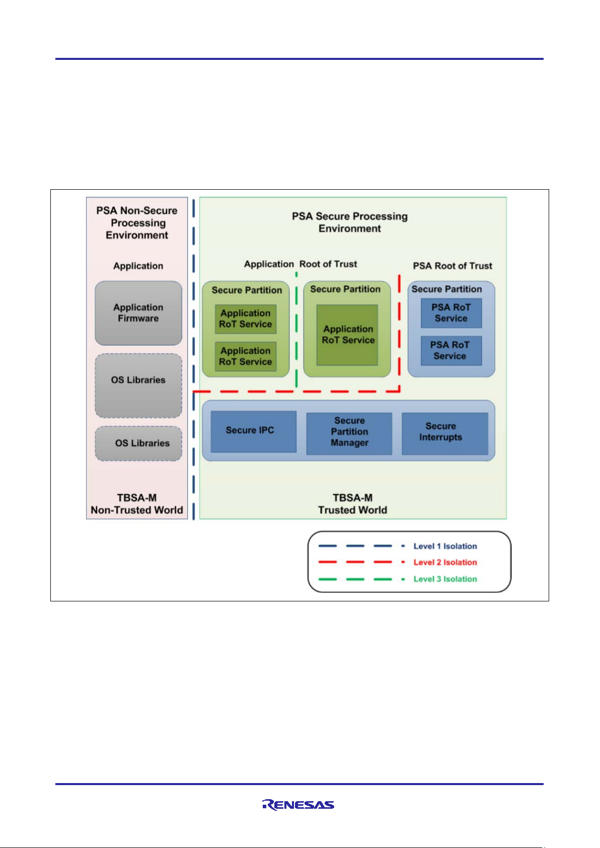
2.1 Introduction to the PSA Isolation Level 2
There are three PSA isolation levels as shown in Figure 5. Note that in general, PSA Isolation Levels are
independent of PSA Certification Level requirements.
PSA Isolation Level 1 requires isolation of the Secure Processing Environ me nt ( SPE) from the rest of the
system. Isolation Level 1 or greater is required for PSA Certified Level 1.
PSA Isolation Level 2 requires isolation of PSA RoT from the rest of the secure partitions within the SPE.
Isolation Level 2 or greater is required for PSA Certified Level 2.
PSA Isolation Level 3 requires isolation of all secure partitions from each other.
Figure 5. PSA Isolation Scheme
R11AN0493EU0100 Rev.1.00 Page 8 of 33
Mar.4.21
Page 9

Renesas RA Family Using Trusted Firmware-M (TF-M) with FSP v2.0.3
2.2 T esting of P SA Level 2 Implementation
Evaluation Labs use vulnerability analysis and penetration testing of the PSA-RoT to confirm if the nine
security requirements of the PSA-RoT Protection Profile have been addressed by the Target of Evaluation.
These nine security requirements, that is, security functions, as defined in the PSA-RoT Lightweight
Protection Profile are:
• Initialization
• Software Isolation
• Secure Storage
• Firmware Update
• Secure State
• Crypto
• Attestation
• Audit
• Debug
There are seven injected threats for the evaluation of the system for PSA Level 2 Certification:
• Remote attacks
• Data injection
• Rogue code execution
• Cryptographic attacks
• RNG
• Brute force
• Side-channel
• Physical attacks
• Probing
• Perturbation
For details on the definition of the security requirement, threat model and step by step guidance on PSA
Certified Level 2, please reference the PSA Certified webpage:
https://www.psacertified.org/development-resources/certification-resources/
2.3 Certification of PSA CertifiedTM Level 2 with TF-M
The Renesas RA MCU RA6M4 MCU Group is PSA Certified Level 2 using FSP v2.0.3 with integrated TF-M
v1.1.
R11AN0493EU0100 Rev.1.00 Page 9 of 33
Mar.4.21
Page 10
Renesas RA Family Using Trusted Firmware-M (TF-M) with FSP v2.0.3
3. Using TFM V1.1 with FSP v2.0.3
Please use the following sections to exercise the TF-M usage with FSP 2.03. The Bootloader will be brought
into the project with a pair of secure and non-secure projects. The debug methodology, secure region
configuration as well as provisioning steps are explained to allow the user to customize the projects.
3.1 Using the TF-M Bootloader and Debug the Skeleton Projects
The skeleton project package Using_TFM_with_FSP_v203_EK_RA6M4.zip includes the TF-M
Bootloader project, initial secure and non-secure projects.
User can use this package as a starting point to debug and customize secure and non-secure applications
following section 3.2. Once the secure and non-secure app licat ion developments are finished, user can
proceed with locking of the Bootloader following the steps explained in section 3.3 and subsequently disable
the debug and serial programming interface following the s teps expla in ed in sect i on 3.4.
1. Install the FSP v2.0.0 platform installer as well as FSP v2.0.3, Python and SEGGER J-Link tools. J-Link
version v6.86 and later should be used.
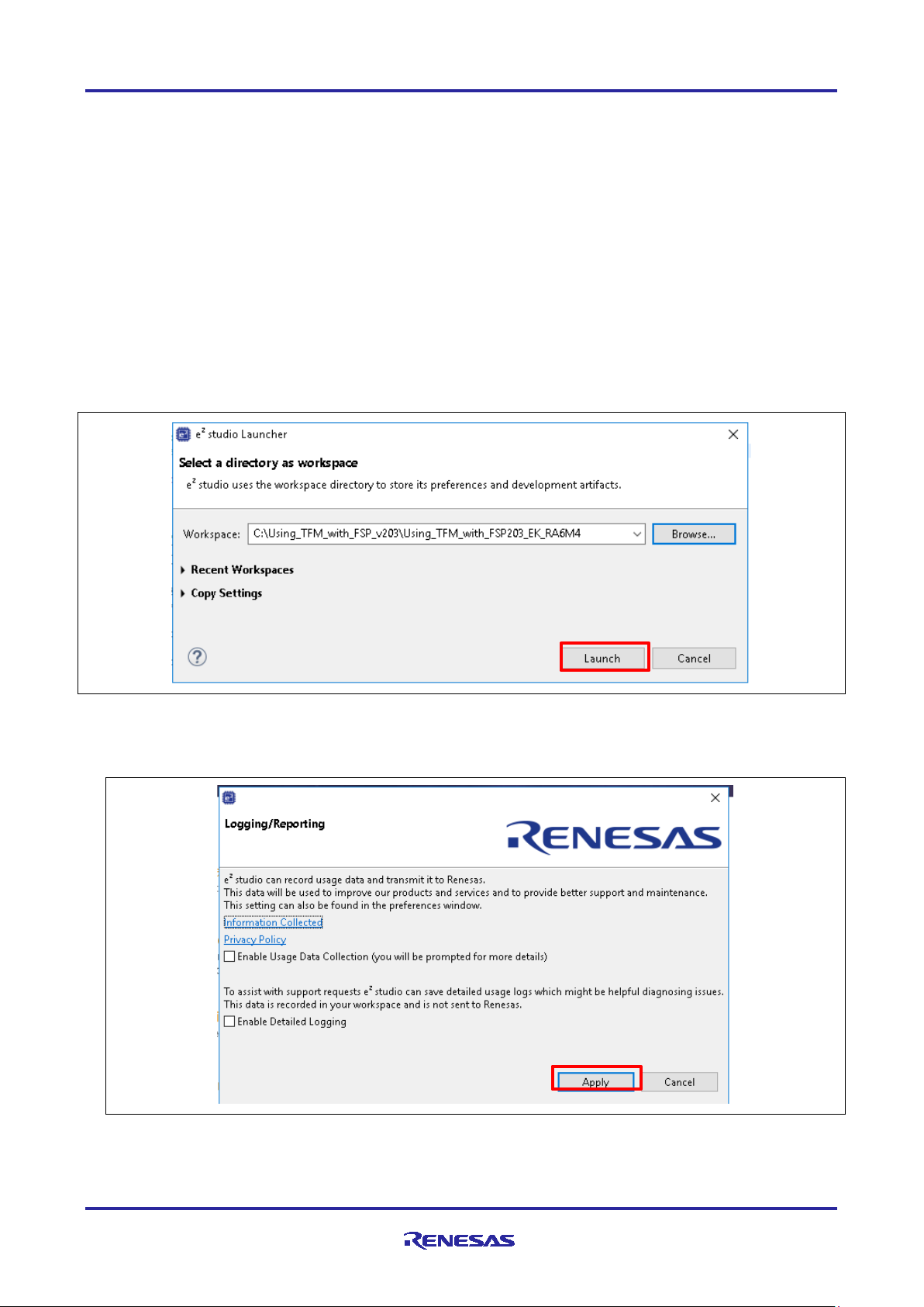
2. Open e
2
studio and select a suitable folder for the workspace that will contain the projects.
Figure 6. Open the Workspace
3. Click Launch and Apply on the Logging/Reporting dialog if it is shown.
Figure 7. Click “Apply”
R11AN0493EU0100 Rev.1.00 Page 10 of 33
Mar.4.21
Page 11
Renesas RA Family Using Trusted Firmware-M (TF-M) with FSP v2.0.3
4. Close the Welcome tab if shown.
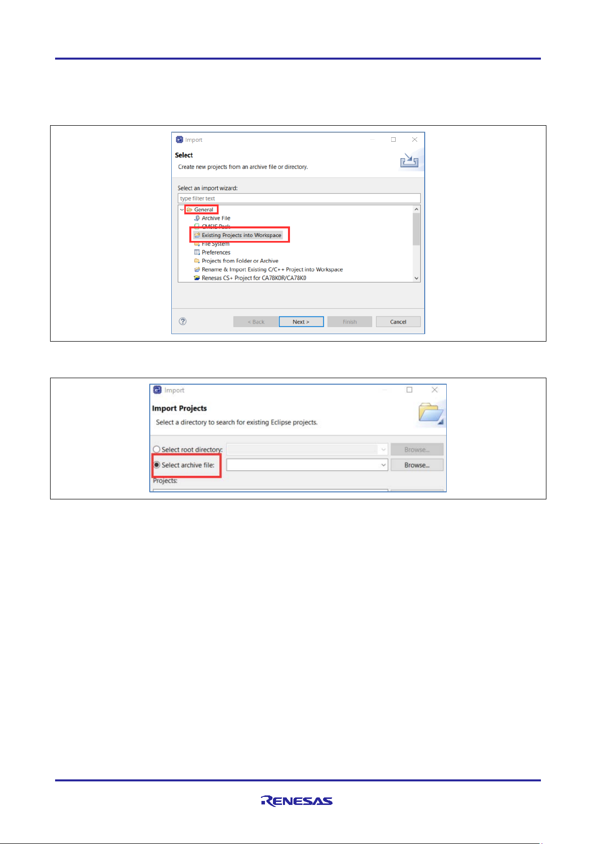
5. We will now import the 3 supplied projects into the workspace. Select File -> Import…
6. Expand General and select Existing Projects into Workspace.
Figure 8. Import Existing Projects
7. Enable the Select archive f ile radio button.
Figure 9. Select the Archive File
R11AN0493EU0100 Rev.1.00 Page 11 of 33
Mar.4.21
Page 12

Renesas RA Family Using Trusted Firmware-M (TF-M) with FSP v2.0.3
8. Click Browse and navigate to the supplied zip file Using_TFM_with_FSP_v203_EK_RA6M4.zip. Click
Open.
9. Make sure the 3 projects are selected and click Finish.
Figure 10. Import all Three Projects
10. The 3 projects should be imported into the workspace:
A. bl2_s – This is the secure BL2 bootloader project
B. tfm_s – This is the secure project containing TF-M
C. tfm_ns – This is the non-secure application project making use of TF-M services.
11. Expand the tfm_s pr oj ect and dou ble-click on the file configuration.xml. This file may take several
seconds to open.
12. TF-M has already been added to this project and configured. Do not worry about the red text in the “Mbed
Crypto” box. This is warning about the heap and stack sizes but in this instance can be ignored. Click
Generate Project Content button. This will extract all the required files from the FSP pack files.
13. Make sure “tfm_s” is highlighted and right-click and select Build Project.
Figure 11. Build tfm-s Project
R11AN0493EU0100 Rev.1.00 Page 12 of 33
Mar.4.21
Page 13

Renesas RA Family Using Trusted Firmware-M (TF-M) with FSP v2.0.3
14. The build will take a few minutes depending on the speed of the computer.
15. The final image should be around 218 kB in size.
16. Repeat steps 10 to 13 for the tfm_ns project.
17. This project should be around 13 kB in size.
18. Repeat steps 10 to 13 for the bl2_s bootloader project.
19. This project should be around 94 kB in size.
3.2 Debugging th e Projects
Next, we will load the projects into the RA6M4 so they can run via the on-board the J-Link debugger. This will
involve:
• Setting the ranges of the secure, non-secure and non-secure callable memory partitions
• Signing the tfm_s and tfm_ns images
• Using SEGGER’s J-Flash Lite to program the tfm_s and tfm_ns signed images
• Finally use the debugger to load the image and symbols for bl2_s and the symbols only for tfm_s and
tfm_ns.
The memory map of the final combined projects is shown below.
Figure 12. Memory Usage of the Secure and Non-secure Regions
1. Within e
Ensure Set TrustZone secure / non-secure boundaries is the only tick-box selected. Set the Device
Family to Renesas RA.
Code Flash Secure: 318
Code Flash NSC: 2
Data Flash Secure: 4
SRAM Secure: 127
SRAM NSC: 1
R11AN0493EU0100 Rev.1.00 Page 13 of 33
Mar.4.21
2
studio select Run > Renesas Device Partition Manager. The settings should be as shown.
Page 14

Renesas RA Family Using Trusted Firmware-M (TF-M) with FSP v2.0.3
Figure 13. Launch Renesas Device Partition Manager
Once the Renesas Device Part itio n Man age r is launched, set up the memory regions as shown below.
Figure 14. Set up the IDAU Regions
2. Plug a micro-USB cable between the host PC and J10 on the EK-RA6M4 board. If the board has
previously been connected, unplug and re-plug the cable at this point.
3. Click Run.
Next we will sign the tfm_s and tfm_ns images.
4. Using Windows
®
File Explorer or equivalent navigate to the scripts folder in the bl2_s project.
bl2_s\ra\arm\trusted-firmware-m\bl2\ext\mcuboot\scripts
R11AN0493EU0100 Rev.1.00 Page 14 of 33
Mar.4.21
Page 15
Renesas RA Family Using Trusted Firmware-M (TF-M) with FSP v2.0.3
5. Open for editing the batch file Sign_S_and_NS.bat. This file calls the various tools to manipulate and
sign the binaries to create the images compatible with the bootloader.
6. On line 2 set the variable elffile_s to point to the tfm_s.elf file in the Debug folder of the tfm_s
project.
7. On line 3 set the variable binfile_s to point to where the output binary file should be written and the
filename.
8. On line 4 set the variable elffile_ns to point to the tfm_ns.elf file in the Debug folder of the
tfm_ns project.
9. On line 5 set the variable binfile_ns to point to where the output binary file should be written and the
filename.
10. On line 8 set the key variable to point to the RSA 3K key used to sign the images. This key is called
root-rsa-3072.pem.
\bl2_s\ra\arm\trusted-firmware-m\bl2\ext\mcuboot\root-rsa-3072.pem
11. On line 10 set the variable flash_layout to the file flash_layout_s.c which is located one folder
up from the location of the batch file being edited. This file is empty but is a requirement of the signing
tool.
\bl2_s\ra\arm\trusted-firmware-m\bl2\ext\mcuboot\scripts\flash_layout_s.c
12. On line 16 set the variable python_path to point to the location of the Python installation.
13. One line 18 set the variable gcc_path to point to the location of the GCC compiler tools and in particular
arm-none-eabi-objcopy.exe.
14. Save this batch file and then open a command (DOS) window in the folder containing the batch file.
15. Call the batch file Sign_S_and_NS.bat which should run and create the signed images. If there are any
problems, check the previous steps for mistakes. Note that Python 3.8.3 is the tested version. After
Python 3.8.3 is installed, pip version needs to be upgraded to latest version prior to install the
dependencies defined in the requirements.txt file.
pip install –upgrade pip
pip3 install --user -r requirements.txt
16. Using Windows
installed, for example, C:\Program Files (x86)\SEGGER\JLink_V686
17. Run JFlashLite.exe
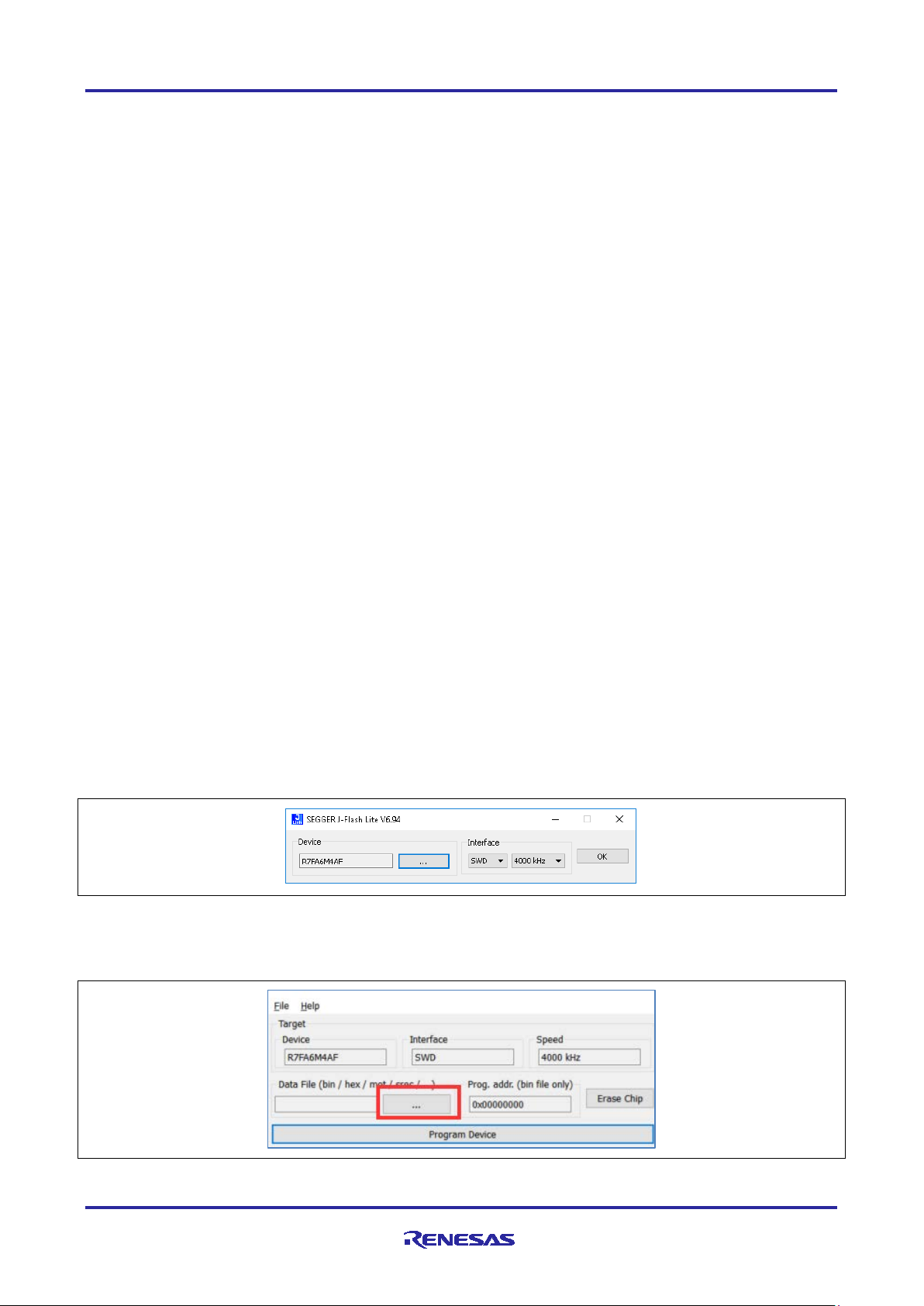
18. Click OK on the production use warning.
19. Configure J-Flash Lite as shown and click OK.
®
File Explorer or equivalent navigate to the folder where the SEGGER tools were
Figure 15. Configure J-Flash
20. Click on the “…” button to navigate to the file to be programmed.
Figure 16. Select Binaries for Prog ramming
R11AN0493EU0100 Rev.1.00 Page 15 of 33
Mar.4.21
Page 16
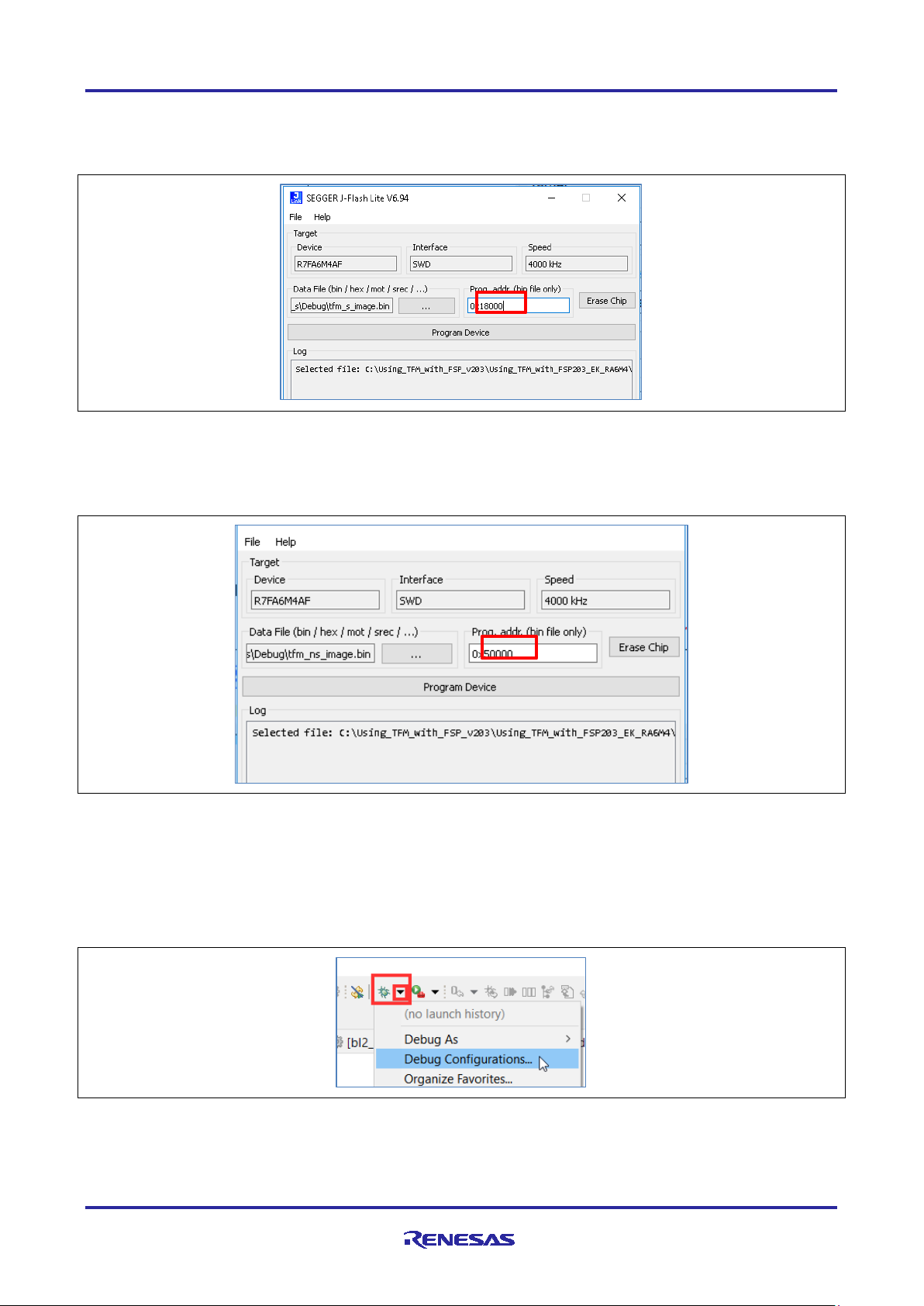
Renesas RA Family Using Trusted Firmware-M (TF-M) with FSP v2.0.3
21. Select the secure image file first tfm_s_image.bin in the folder \tfm_s\Debug.
22. Set the Program address to 0x18000 as shown.
Figure 17. Set the Secure Application Programming Location
23. Click on Program Device.
24. Repeat these steps to program tfm_ns_image.bin in \tfm_ns\Debug at address 0x50000.
Figure 18. Set the Non-secure Application Programming Location
Next, we will use the debugger to download the bootloader image and the symbols for the other two
images which have been loaded into the MCU flash via J-Flash Lite.
25. In e
2
studio click on the black downwards arrow next to the bug and select Debug Configurations….
Figure 19. Debug bl2_s
R11AN0493EU0100 Rev.1.00 Page 16 of 33
Mar.4.21
Page 17
Renesas RA Family Using Trusted Firmware-M (TF-M) with FSP v2.0.3
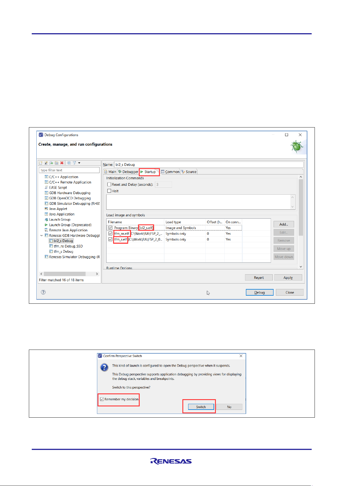
26. On the left expand Renesas GDB Hardware Debug and select bl2_s Debug.
Figure 20. Select bl2_s
27. Select the Debugger tab and then the Connection Settings tab. Scroll to the bottom and make sure the
option Set TrustZone secure/non-secure Boundaries is set to No.
Figure 21. Disable TrustZone Secure/non-secure Boundary Setting from e2 studio
R11AN0493EU0100 Rev.1.00 Page 17 of 33
Mar.4.21
Page 18
Renesas RA Family Using Trusted Firmware-M (TF-M) with FSP v2.0.3
This option stops the tooling from dynamically adjusting the secure/non-secure partitions on every build.
As we are using a bootloader we have pre-defined regions which we previously set up using the Renesas
Partition manager.
This option does not always remain sticky and can switch back to Yes. If execution unexpectedly ends up
in the default handler check this option. If it is set to Yes switch it back to No and reload the boundaries
using the Renesas Partition Manager as described earlier. This is a known Issue and is fixed in FSP v2.3
or later release.
28. Select the Startup tab. Here you will see that the for the bootloader binary bl2_s.elf the image and
symbols will be downloaded. For the bootloader to accept the secure and non-secure images these
images must be signed. This is why they were loaded manually using J-Flash Lite. As such only the
symbols for these images are loaded by the debugger.
Figure 22. Startup Configuration
29. Click Apply and Debug to launch the debug session.
30. If a dialog pops up requesting to switch to the debug perspective, select Remember my decision and
click Switch.
Figure 23. Confirm Perspective Switch
R11AN0493EU0100 Rev.1.00 Page 18 of 33
Mar.4.21
Page 19

Renesas RA Family Using Trusted Firmware-M (TF-M) with FSP v2.0.3
31. Execution will stop in Reset_Handler() in the bootloader. Click the Resume icon or hit F8 to continue.
Figure 24. Running the Application
32. Execution will stop in main() in the bootloader.
33. In the left pane select the Pro g ram Expl o r er tab and expand the tfm_ns project, then expand the src
folder and then double-click new_thread0_entry.c file.
Figure 25. Running the Application
Function new_thread0_entry() is where user code can be added. Currently it contains code to:
• Call TF-M attestation services
• Call TF-M storage services
• Call TF-M crypto services
• Call TF-M flash services
• Show use of a non-secure peripheral, in this case a UART.
34. Place a breakpoint in this function, hit Resume (F8) and examine the execution of this function.
This ends the description of how to debug a TF-M based project compatible with the BL2 bootloader
using Renesas’s EK-RA6M4 and FSP v2.0.3.
R11AN0493EU0100 Rev.1.00 Page 19 of 33
Mar.4.21
Page 20
Renesas RA Family Using Trusted Firmware-M (TF-M) with FSP v2.0.3
3.3 Maki ng the Bootloader Immutable
To make the BL2 bootloader immutable, the flash blocks containing the bootloader should be locked from
being programmed and erased.
The RA6M4 features two sets of registers which facilitate flash block locking. Block Protect Setting (BPS)
Registers feature bits which map to individual flash blocks. When a bit is set to zero the corresponding flash
block is not able to be erased or programmed. The Permanent Block Protect Setting (PBPS) Registers have
a similar bit mapping of flash blocks. When a bit is set in one of these registers, the corresponding flash
block is permanently locked from being eras ed and pr ogram med so long as the same bit in the Block Prot ect
Setting Register is also cleared to zero. This process is irreversible. Once a flash block is permanently
locked, it cannot be unlocked again.
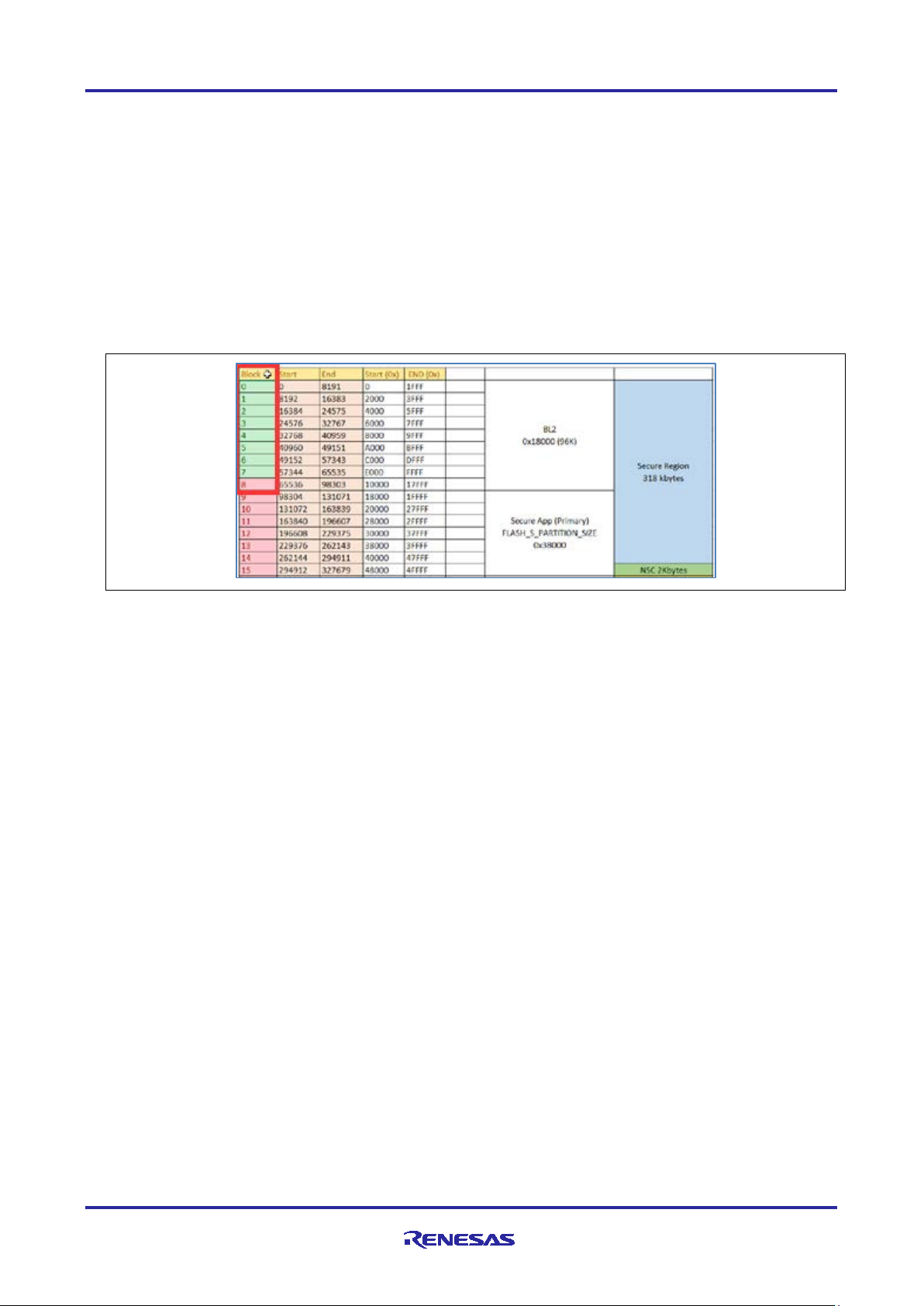
From the memory layout shown below it can be seen that the BL2 bootloader occupies flash blocks 0 to 8
inclusive. Eight 8 kB blocks and one 32 kB block totaling 96 kB.
Figure 26. Running the Application
FSP configurator supports locking of flash blocks and the permanent setting of this lock.
R11AN0493EU0100 Rev.1.00 Page 20 of 33
Mar.4.21
Page 21
Renesas RA Family Using Trusted Firmware-M (TF-M) with FSP v2.0.3
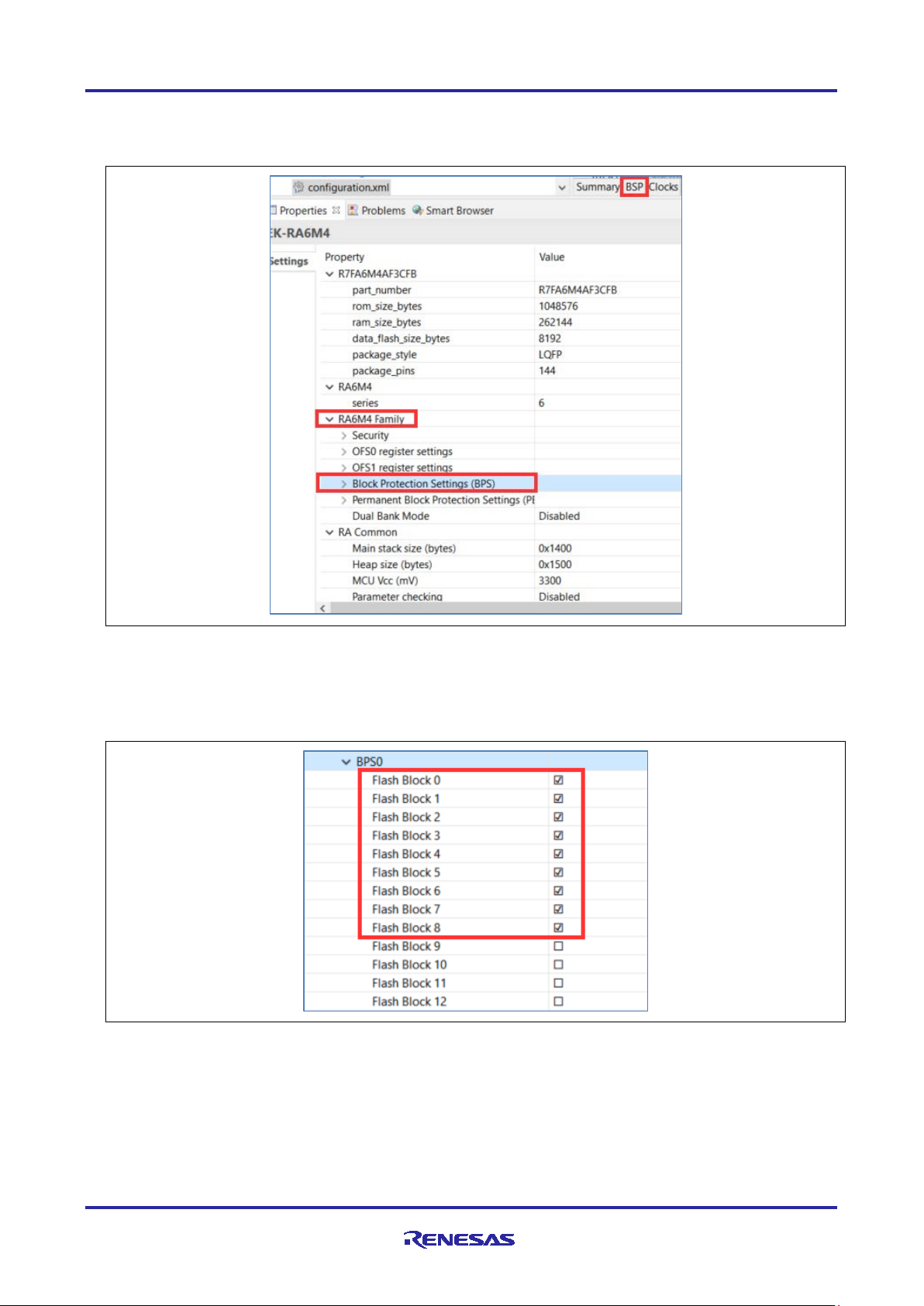
1. Select the bl2_s project and open configuration.xml in the FSP Configuration perspective.
2. Select the BSP tab.
3. In the Properties pane under RA6M4 Family, expand Block Protecti on Set tin gs (BPS).
Figure 27. Select the Block Protection Settings (BPS)
4. Expand this option.
5. Expand BPS0 which contains the flash locking bits for the first 32 flash blocks.
6. Tick Flash Block 0 to Flash Block 8 inclusive to lock the bootloader flash blocks from being programmed
and erased as shown.
Figure 28. Select the BPS Blocks
R11AN0493EU0100 Rev.1.00 Page 21 of 33
Mar.4.21
Page 22
Renesas RA Family Using Trusted Firmware-M (TF-M) with FSP v2.0.3
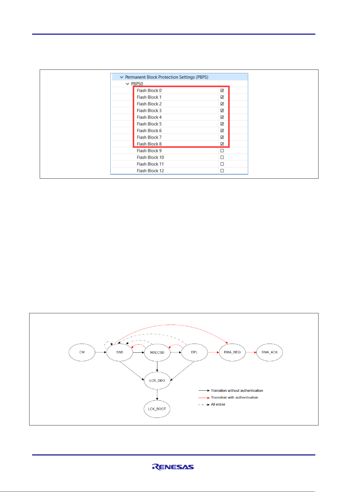
7. To make this flash protection permanent, expand Permanent Block Protection Settings (PBSP) option.
8. Expand PBPS0 which contains the permanent flash locking bits for the first 32 flash blocks.
9. Tick Flash Block 0 to Flash Block 8 inclusive to p er m anen tly lock the bootlo ader f lash blocks from being
programmed and erased as shown.
Figure 29. Select the PBPS Blocks
10. Click Gen e rate Project Content and build the bl2_s project.
11. Program the BL2 bootloader into the board following the section 3.2 instructions.
Note: Ticking the BSP0 and PBPS0 Flash Block settings will permanently lock the flash blocks. This
CANNOT be reversed. Further details can be found in sections 6.2.6 and 6.2.7 of the RA6M4
hardware manual.
3.4 Device Lifecycle Management – Disabling the Debug and Factory Programming
Interfaces
The RA6M4 device lifecycle identifies the current phase of the device and controls the capabilities of the
debug interface and serial programming interface.
Consider the device lifecycles shown below and described in section 49.3 in the RA6M4 hardware manual.
Figure 30. Device Lifecycle Management
R11AN0493EU0100 Rev.1.00 Page 22 of 33
Mar.4.21
Page 23

Renesas RA Family Using Trusted Firmware-M (TF-M) with FSP v2.0.3
In the LCK_DBG state the debug interface is disabled but the serial programming interface is still accessible.
In the LCK_BOOT state, the debug interface is disabled, and the serial programming interface is also
disabled. Please note, as shown in the diagram once the lifecycle setting moves to LCK_BDG and/or
LCK_BOOT it cannot be reversed.
The DLM state of a device can be modified only via the serial programming interface and cannot be
manipulated from the application program. Use Renesas Flash Programmer v3.08.00d or later.
To change the DLM state:
1. Launch Renesas Flash Programmer v3.08.00d.
2. Select File > New Project
3. Set Microcontroller to RA, name the project and choose J-Link as the communication tool.
Figure 31. Create a New RFP Project
4. With the board connected to the PC, click on Connect. It may be necessary to disconnect the USB
cable(s) and reconnect the debug USB cable and try again.
5. The current DLM state and other options can be displayed via Device Information > Read Flash
Options
Figure 32. Read the Device Flash Configuration
The Boundary values should be familiar from those set earlier using the Renesas Device Partition
Manager.
R11AN0493EU0100 Rev.1.00 Page 23 of 33
Mar.4.21
Page 24

Renesas RA Family Using Trusted Firmware-M (TF-M) with FSP v2.0.3
6. To change the DLM state switch to the Flash Options tab.
7. Set the DLM Set Option to Set.
8. Set the DLM Target State required.
If setting the DLM state to LCK_DBG or LCK_BOOT, a warning that this option is not reversible will be
displayed.
Figure 33. Transition to LCK_BOOT
Transition to LCK_BOOT is irr ever s ible.
Figure 34. Warning
R11AN0493EU0100 Rev.1.00 Page 24 of 33
Mar.4.21
Page 25

Renesas RA Family Using Trusted Firmware-M (TF-M) with FSP v2.0.3
9. Switch to the Operations Settings tab and in the Command section, ensure only Program Flash
Options and Verify Flash Options are set.
Figure 35. Set Flash Options Program/Verify
10. Switch to the Operation tab.
11. The Flash Operation should be shown as Program Flash Options > Verify Flash Options.
12. Click Start to set the flash options and so the DLM state.
Note: As previously mentioned, it is not possible to reverse changing the DLM state to LCK_DBG or
LCK_BOOT.
3.5 Customizing a Renesas TF-M Implementation for an End Product
When the TF-M is used as a template for an end product, a few items must be customized for that
application.
Immutable flash blocks
The secure bootloader is stored in immutable flash, as described above. If the secure bootloader is modified,
the memory map of the built image must be examined to ensure that the correct flash blocks are locked.
This may require locking more or fewer flash blocks than as shown in the demo, requiring more or fewer
BPS0 and PBPS0 Flash Block x options ticked, as shown above.
TrustZone configuration
The configuration of the IDAU registers for TrustZone configuration is handled by the tooling, following the
steps described above.
Key provisioning
For straight-forward integration with TF-M, the following PSA-defined keys need to be uniquely provisioned
for each MCU:
R11AN0493EU0100 Rev.1.00 Page 25 of 33
Mar.4.21
Page 26

Renesas RA Family Using Trusted Firmware-M (TF-M) with FSP v2.0.3
Hardware-Unique Key (HUK) for TF-M key derivation
If TF-M key derivation is utilized, then an HUK must be securely provisioned. It is recommended to use an
HSM for secure key generation. Space for a 256-bit HUK is reserved in the project file
\ra\fsp\src\rm_tfm_port\ra\tfm_initial_attestation_key_material.c, the location of
which can be found by examining the map file as shown below. The externally generated key should be
securely programmed at that location during the programming of the secure image.
Figure 36. Program the Externally Generated Key
Initial Attestation Key (IAK)
If attestation is used in the end product deployment, an MCU-unique IAK needs to be securely provisioned,
with the private key residing on the MCU and the public key available to the deployment infrastructure. It is
recommended to use an HSM for secure key generation of ECC secp256r1 (NIST Curve P-256) key pairs.
Space for the private key is reserved in the project file
\ra\fsp\src\rm_tfm_port\ra\tfm_initial_attestation_key_material.c, the location of
which can be found by examining the map file as shown below. It should be securely programmed during
the programming of the secure image.
Figure 37. Program the Initial Attestation Key
In addition, the following PSA-defined keys need to be defined and provisioned as per the end product use
case:
Image Signing Key (ROTPK)
Images are signed with a private key and verified on the MCU with the corresponding public key. This key
pair is typically not MCU-unique, but rather used across a range of devices. The application developer is
responsible for secure key management of the private key. The public key can either be provisioned at the
same time that the bootloader is programmed, or it can be incorporated into the bootloader firmware itself, as
shown by the TF-M Demo.
The default public key is located in the bl2_s bootloader project, in the file \ra\arm\trusted-
firmware-m\bl2\ext\mcuboot\keys.c. The default private key is located in the same project and
folder in the file root-rsa-3072.pem, this key is used to sign the secure image. The bootloader supports
two signing keys, with the second private key in the file root-rsa-3072_1.pem, which is used to sign the
non-secure image. Note that in a final product, the private key(s) must be handled securely; storing them
with the bootloader project sour ce code is not recommended.
R11AN0493EU0100 Rev.1.00 Page 26 of 33
Mar.4.21
Page 27

Renesas RA Family Using Trusted Firmware-M (TF-M) with FSP v2.0.3
4. Example Project for Firmware Update
This firmware downloader functionality needs to be pre-loaded to the MCU prior to lock the Bootloader. Once
the TF-M Bootloader is locked up permanently, the only way to get a new image into the device is via the NS
application with downloader functionality. If an image is created and sent to the board without the ability to
download a new image, there will be no way to make further image updates.
4.1 Import a nd Dow nl oad the Example Firmware Update Project
The zip file Renesas_EK_RA6M4_XModem_BLS_TFM_Downlaoder.zip contains 3 projects: the BL2
bootloader, TF-M secure projects and a TF-M based non-secure project which contains the XModem
downloader.
To build and use these projects, follow the instruc t ions of section 3.1 and make the following substitutions:
Use BL2 project EK_RA6M4_BL2_BL_TOE in pl ac e of the bl2_s project.
Use secure project EK_RA6M4_BL2_TFM_TOE_S in place of the tfm_s project.
Use non-secure application project EK_RA6M4_BL2_App_TOE_NS in place of the tfm_ns project.
The secure and non-secure boundary of this firmware update project is same as the Skeleton project. Follow
section 3.2 to set up the secure and non-secure boundary, program the secure and non-secure image and
then start the debug session.
Note that for this downloader application, both J10 (J-Link On-Board debugger) and J11 (USB CDC) need to
be connected. The USB CDC port will be receiving the new images.
4.2 Running the Example Firmware Downloader Application
1. Once the debug session started from project EK_RA6M4_BL2_BL_TOE, start a terminal emulator,
TeraTerm used is used as example here, an connect it to the COM port presented by the board. The
below menu should be displayed. The blue user LED should be flashing when the board is powered up.
Figure 38. TeraTerm Menu Prompt
R11AN0493EU0100 Rev.1.00 Page 27 of 33
Mar.4.21
Page 28

Renesas RA Family Using Trusted Firmware-M (TF-M) with FSP v2.0.3
2. Menu option 1 displays the header information from primary non-secure slot (the slot currently executing),
the secondary secure slot (upgrade slot) and secondary non-secure slot (upgrade slot). Note that
depending on whether the secondar y slots have had i mages or not previously, the print out may differ.
Figure 39. Display Header Information
R11AN0493EU0100 Rev.1.00 Page 28 of 33
Mar.4.21
Page 29

Renesas RA Family Using Trusted Firmware-M (TF-M) with FSP v2.0.3
3. After successful execution of option 1, it is recommended to restart the debug session from project
EK_RA6M4_BL2_BL_TOE prior to proceed to the secure image downloading. Menu option 2 allows a
new secure image to be downloaded via the XModem protocol. The supplied zip file
Renesas_EK_RA6M4_XModem_BLS_TFM_Downlaoder.zip contains a test secure image –
Pre_Built_S_TFM_Image/EK_RA6M4_BL2_TFM_TOE_S_image.bin.
Note: Be sure to select a secure (S) image to avoid the risk of downloading an incorrect image and
making the board unrecoverable.
Using TeraTerm press “2” and then download the image via File > Transfer > XMODEM > Send
Figure 40. Send the Secure Image
Select the Prebuilt secur e image. If the version of your TeraTerm has option to select Check sum under this
window, enable the Chec ksum option. Most TeraTer m versions have this enabled by default. In this case,
there will be no need to configure this option.
Figure 41. Select the Prebuilt Secure Image
R11AN0493EU0100 Rev.1.00 Page 29 of 33
Mar.4.21
Page 30

Renesas RA Family Using Trusted Firmware-M (TF-M) with FSP v2.0.3
Figure 42. Download the Secure Image
4. To download a NS image used option 3. It is recommended to restart the debug session from project
EK_RA6M4_BL2_BL_TOE prior to proceed to the non-secure image downloading. Test images are
supplied in the zip file Renesas_EK_RA6M4_XModem_BLS_TFM_Downlaoder.zip in
Pre_Built_NS_Images.
Figure 43 Non-secure Test Image
Select one of the images and download using the XModem protocol as described in the step 3.
Note: Be sure to select a non-secure (NS) image to avoid the risk of downloading an incorrect image and
making the board unrecoverable.
5. Use option 4 to reboot the device. There will be a delay while the bootloader verifies the new images and
updates the primary slots. The new images will then run.
R11AN0493EU0100 Rev.1.00 Page 30 of 33
Mar.4.21
Page 31

Renesas RA Family Using Trusted Firmware-M (TF-M) with FSP v2.0.3
5. References
1. Arm Platform Security Architecture Overview
2. Why Arm Platform Security Architecture
3. Arm PSA Certification
4. Arm PSA Developer Website
R11AN0493EU0100 Rev.1.00 Page 31 of 33
Mar.4.21
Page 32

Renesas RA Family Using Trusted Firmware-M (TF-M) with FSP v2.0.3
6. Website and Support
Visit the following URLs to learn about the RA family of microcontrollers, download tools and documentation,
and get support.
EK-RA6M4 Resources renesas.com/ra/ek-ra6m
RA Product Information renesas.com/ra
Flexible Software Package (FSP) renesas.com/ra/fsp
RA Product Support Forum renesas.com/ra/forum
Renesas Support renesas.com/support
4
R11AN0493EU0100 Rev.1.00 Page 32 of 33
Mar.4.21
Page 33
Renesas RA Family Using Trusted Firmware-M (TF-M) with FSP v2.0.3
Rev.
Date
Description
Page
Summary
1.00
Mar.4.21
-
First release document
Revision History
R11AN0493EU0100 Rev.1.00 Page 33 of 33
Mar.4.21
Page 34

Corporate Headquarters
Contact information
Trademarks
Notice
1. Descriptions of circuits, software and other related information in this document are provided only to illustrate the operation of semiconductor products
and application examples. You are fully responsible for the incorporation or any other use of the circuits, software, and information in the desi gn of you r
product or system. Renesas Electronics disclaims any and all liability for any losses and damages incurred by you or third parties arising from the use
of these circuits, software, or information.
2. Renesas Electronics hereby expressly disclaims any warranties against and liability for infringement or any other claims involving patents, copyrights,
or other intellectual property rights of third parties, by or arising from the use of Renesas Electronics products or technical information described in this
document, including but not limited to, the product data, drawings, charts, programs, algorithms, and application examples.
3. No license, express, implied or otherwise, is granted hereby under any patents, copyrights or other intellectual property rights of Renesas Electronics
or others.
4. You shall be responsible for determining what licenses are required from any third parties, and obtaining such licenses for the lawful import, export,
manufacture, sales, utilization, distribution or other disposal of any products incorporating Renesas Electronics products, if required.
5. You shall not alter, modify, copy, or reverse engineer any Renesas Electronics product, whether in whole or in part. Renesas Electronics disclaims any
and all liability for any losses or damages incurred by you or third parties arising from such alteration, modification, copying or reverse engineering.
6. Renesas Electronics products are classified according to the following two quality grades: “Standard” and “High Quality”. The intended applications for
each Renesas Electronics product depends on the product’s quality grade, as indicated below.
"Standard": Computers; office equipment; communications equipment; test and measurement equipment; audio and visual equipment; home
"High Quality": Transportation equipment (automobiles, trains, ships, etc.); traffic control (traffic lights); large-scale communication equipment; key
Unless expressly designated as a high reliability product or a product for harsh environments in a Renesas Electronics data sheet or other Renesas
Electronics document, Renesas Electronics products are not intended or authorized for use in products or systems that may pose a direct threat to
human life or bodily injury (artificial life support devices or systems; surgical implantations; etc.), or may cause serious property damage (space
system; undersea repeaters; nuclear power control systems; aircraft control systems; key plant systems; military equipment; etc.). Renesas Electronics
disclaims any and all liability for any damages or losses incurred by you or any third parties arising from the use of any Renesas Electronics product
that is inconsistent with any Renesas Electronics data sheet, user’s manual or other Renesas Electronics document.
7. No semiconductor product is absolutely secure. Notwithstanding any security measures or features that may be implemented in Renesas Electronics
hardware or software products, Renesas Electronics shall have absolutely no liability arising out of any vulne ra bil ity or secu ri ty br eac h, includi ng bu t
not limited to any unauthorized access to or use of a Renesas Electronics product or a system that uses a Renesas Electronics product. RENESAS
ELECTRONICS DOES NOT WARRANT OR GUARANTEE THAT RENESAS ELECTRONICS PRODUCTS, OR ANY SYSTEMS CREATED USING
RENESAS ELECTRONICS PRODUCTS WILL BE INVULNERABLE OR FREE FROM CORRUPTION, ATTACK, VIRUSES, INTERFERENCE,
HACKING, DATA LOSS OR THEFT, OR OTHER SECURITY INTRUSION (“Vulnerability Issues”). RENESAS ELECTRONICS DISCLAIMS ANY AND
ALL RESPONSIBILITY OR LIABILITY ARISING FROM OR RELATED TO ANY VULNERABILITY ISSUES. F URTHERMORE, TO THE EXTENT
PERMITTED BY APPLICABLE LAW, RENESAS ELECTRONICS DISCLAIMS ANY AND ALL WARRANTIES, EXPRESS OR IMPLIED, WITH
RESPECT TO THIS DOCUMENT AND ANY RELATED OR ACCOMPANYING SOFTWARE OR HARDWARE, INCLUDING BUT NOT LIMITED TO
THE IMPLIED WARRANTIES OF MERCHANTABILITY, OR FITNESS FOR A PARTICULAR PURPOSE.
8. When using Renesas Electronics products, refer to the latest product information (data sheets, user’s manuals, application notes, “General Notes for
Handling and Using Semiconductor Devices” in the reliability handbook, etc.), and ensure that usage conditions are within the ranges specified by
Renesas Electronics with respect to maximum ratings, operating power supply voltage range, heat dissipation characteristics, installation, etc. Renesas
Electronics disclaims any and all liability for any malfunctions, failure or accident arising out of the use of Renesas Electronics product s outsi de of such
specified ranges.
9. Although Renesas Electronics endeavors to improve the quality and reliability of Renesas Electronics products, semiconductor products have specific
characteristics, such as the occurrence of failure at a certain rate and malfunctions under certain use conditions. Unless designated as a high reliability
product or a product for harsh environments in a Renesas Electronics data sheet or other Renesas Electronics document, Renesas Electronics
products are not subject to radiation resistance design. You are responsible for implementing safety measures to guard against the possibility of bodily
injury, injury or damage caused by fire, and/or danger to the public in the event of a failure or malfunction of Renesas Electronics products, suc h as
safety design for hardware and software, including but not limited to redundancy, fire control and malfunction prevention, appropriate treatment for
aging degradation or any other appropriate measures. Because the evaluation of microcomputer software alone is very difficult and impractical, you are
responsible for evalu atin g the s af ety of t he final products or systems manufactured by you.
10. Please contact a Renesas Electronics sales office for details as to environmental matters such as the environmental compatibil ity of each Renesas
Electronics product. You are responsible for carefully and sufficiently investigating applicable laws and regulations that regulate the inclusion or use of
controlled substances, including without limitation, the EU RoHS Directive, and using Renesas Electronics products in compliance with all these
applicable laws and regulations. Renesas Electronics disclaims any and all liability for damages or losses occurring as a result of your noncompliance
with applicable laws and regulations.
11. Renesas Electronics products and technologies shall not be used for or incorporated into any products or systems whose manufacture, use, or sale is
prohibited under any applicable domestic or foreign laws or regulations. You shall comply with any applicable export control laws and regulations
promulgated and administered by the governments of any countries asserting jurisdiction over the parties or transactions.
12. It is the responsibility of the buyer or distributor of Renesas Electronics products, or any other party who distributes, disposes of, or otherwise sells or
transfers the product to a third party, to notify such third party in advance of the contents and conditions set forth in this document.
13. This document shall not be reprinted, reproduced or duplicated in any form, in whole or in part, without prior written consent of Renesas Electronics.
14. Please contact a Renesas Electronics sales office if you have any questions regarding the information contained in this document or Renesas
Electronics products.
(Note1) “Renesas Electronics” as used in this document means Renesas Electronics Corporation and also includes its directly or indirectly controlled
(Note2) “Renesas Electronics product(s)” means any product developed or manufactured by or for Renesas Electronics.
subsidiaries.
electronic appliances; machine tools; personal electronic equipment; industrial robots; etc.
financial terminal systems; safety control equipment; etc.
(Rev.5.0-1 October 2020)
TOYOSU FORESIA, 3-2-24 Toyosu,
Koto-ku, Tokyo 135-0061, Japan
www.renesas.com
Renesas and the Renesas logo are trademarks of Renesas Electronics
Corporation. All trademarks and registered trademarks are the property
of their respective owners.
For further information on a product, technology, the most up-to-date
version of a document, or your ne are s t sales office, please visit:
www.renesas.com/contact/
.
© 2021 Renesas Electronics Corporation. All rights reserved.
 Loading...