

Page 1

Release Note
R20UT4487ES0291 Rev.2.91 Page 1 of 36
Apr.13.21
Smart Configurator for RX V2.9.1
Release Note
Introduction
Thank you for using the Smart Configurator for RX.
This document describes the restrictions and points for caution. Read this document before using the
product.
Contents
1. Introduction .............................................................................................................................. 3
1.1 System requirements ......................................................................................................................... 3
1.1.1 PC ................................................................................................................................................... 3
1.1.2 Development Environments ............................................................................................................. 3
2. Support List ............................................................................................................................. 4
2.1 Support Devices List ................................ ................................................................ .......................... 4
2.2 Support Components List ................................................................................................................... 9
2.3 New support..................................................................................................................................... 15
2.3.1 BSP (Board Support Package) revision update .............................................................................. 15
2.3.2 Toolbar icons update ...................................................................................................................... 15
2.3.3 Software component version number has been added into report ................................................... 15
2.3.4 Generated source files’ folder can be accessed from console window ............................................ 16
3. Changes ................................................................................................................................ 17
3.1 Correction of issues/limitations ......................................................................................................... 17
3.1.1 Fixed the pin codes missing issue when using MTU components ................................................... 18
3.1.2 Fixed the resource change issue when using MTU Normal Mode Timer Component ...................... 18
3.1.3 Fixed the device change issue when using BSP rev5.63 ................................ ................................ 18
3.1.4 Fixed the generated codes’ folder issue for FreeRTOS (with IoT libraries) project ........................... 18
3.1.5 Fixed the interrupt migration report status issue when performing the device change without opening
Smart Configurator GUI.................................................................................................................. 18
3.1.6 Fixed the configurable issue for PH7 when using PORT component ............................................... 18
3.2 Specification changes ...................................................................................................................... 19
3.2.1 Improved the Import and Export function layouts for the Board and Pins pages .............................. 20
3.2.2 Drop-down list items of the “Function” selection combo box for the New Component dialog are tidied
up ................................ ................................................................................................ .................. 21
4. List of RENESAS TOOL NEWS AND TECHNICAL UPDATE ................................................ 22
5. Points for Limitation ................................................................ ................................ ............... 26
5.1 List of Limitation ............................................................................................................................... 26
5.2 Details of Limitation .......................................................................................................................... 27
5.2.1 Note on the inconsistent code generation behavior issue when loading existing project with Port
R20UT4487ES0291
Rev.2.91
Apr.13.21
Page 2

Smart Configurator for RX V2.9.1 Release Note
R20UT4487ES0291 Rev.2.91 Page 2 of 36
Apr.13.21
configuration .................................................................................................................................. 27
5.2.2 Note on the general I/O port direction issue on MCU package view when using Port Component ... 27
5.2.3 Note on CLKOUT pin settings issue on the clock page ................................................................... 27
5.2.4 Note on the resource tree in the FIT component GUI configuration ................................................. 27
5.2.5 Note on address bus when using external bus ................................................................................ 28
5.2.6 Note on the FIT component pin configuration issue when changing version .................................... 28
5.2.7 Note on the error icon display issue on the hardware resource tree when performing pin assignment
with selected board ........................................................................................................................ 28
5.2.8 Note on the generated code issue for PDR register when configuring multiplexed GPIO pins by
PORT component .......................................................................................................................... 29
6. Points for Caution .................................................................................................................. 30
6.1 List of Caution .................................................................................................................................. 30
6.2 Details of Caution ............................................................................................................................. 32
6.2.1 Note on configuring GPT interrupts ................................................................................................ 32
6.2.2 Note on SCR.TE bit setting sequence in SCI Clock Synchronous Mode and SCI Clock
Asynchronous Mode ...................................................................................................................... 33
6.2.3 Note on using only reception in SCI Clock Synchronous Mode ....................................................... 33
6.2.4 Note on using high transfer speed in SCIF Synchronous Mode ...................................................... 33
6.2.5 Note on device change functionality ............................................................................................... 34
6.2.6 Note on using Smart Configurator for GCC project in e2 studio 7.4.0 .............................................. 34
6.2.7 Note on configuring GPT interrupts ................................................................................................ 34
6.2.8 Note on using Data Transfer Controller .......................................................................................... 34
6.2.9 Note on Ports setting when using S12AD components ................................................................... 34
6.2.10 Note on section build warning when using FIT components ............................................................ 34
6.2.11 Note on clock frequency usage ...................................................................................................... 35
6.2.12 Note on C++ project support in CS+ and IAR ................................................................................. 35
Revision History ............................................................................................................................ 36
Page 3

Smart Configurator for RX V2.9.1 Release Note
R20UT4487ES0291 Rev.2.91 Page 3 of 36
Apr.13.21
1. Introduction
Smart Configurator is a utility for combining software to meet your needs. It supports the following three
functions related to the embedding of Renesas drivers in your systems: importing middleware, generating
driver code, and setting pins.
1.1 System requirements
The operating environment is as follows.
1.1.1 PC
• IBM PC/AT compatibles (Windows® 10, Windows® 8.1)
• Processor: 1 GHz or higher (must support hyper-threading, multi-core CPUs)
• Memory capacity: 4 GB or more recommended. Minimum requirement is 2 GB or more (64-bit
Windows requires 4 GB or more)
• Hard disk capacity: 200 MB or more spare capacity
• Display: 1024 x 768 or higher resolution, 65,536 or more colors
• All other necessary software environments in addition to Windows OS: Java Runtime Environment
1.1.2 Development Environments
• Renesas electronics Compiler for RX [CC-RX] V3.01.00 or later
• GCC for Renesas 4.8.4.201902 or later
• IAR Embedded Workbench 4.12.1 or later
Page 4
Smart Configurator for RX V2.9.1 Release Note
R20UT4487ES0291 Rev.2.91 Page 4 of 36
Apr.13.21
2. Support List
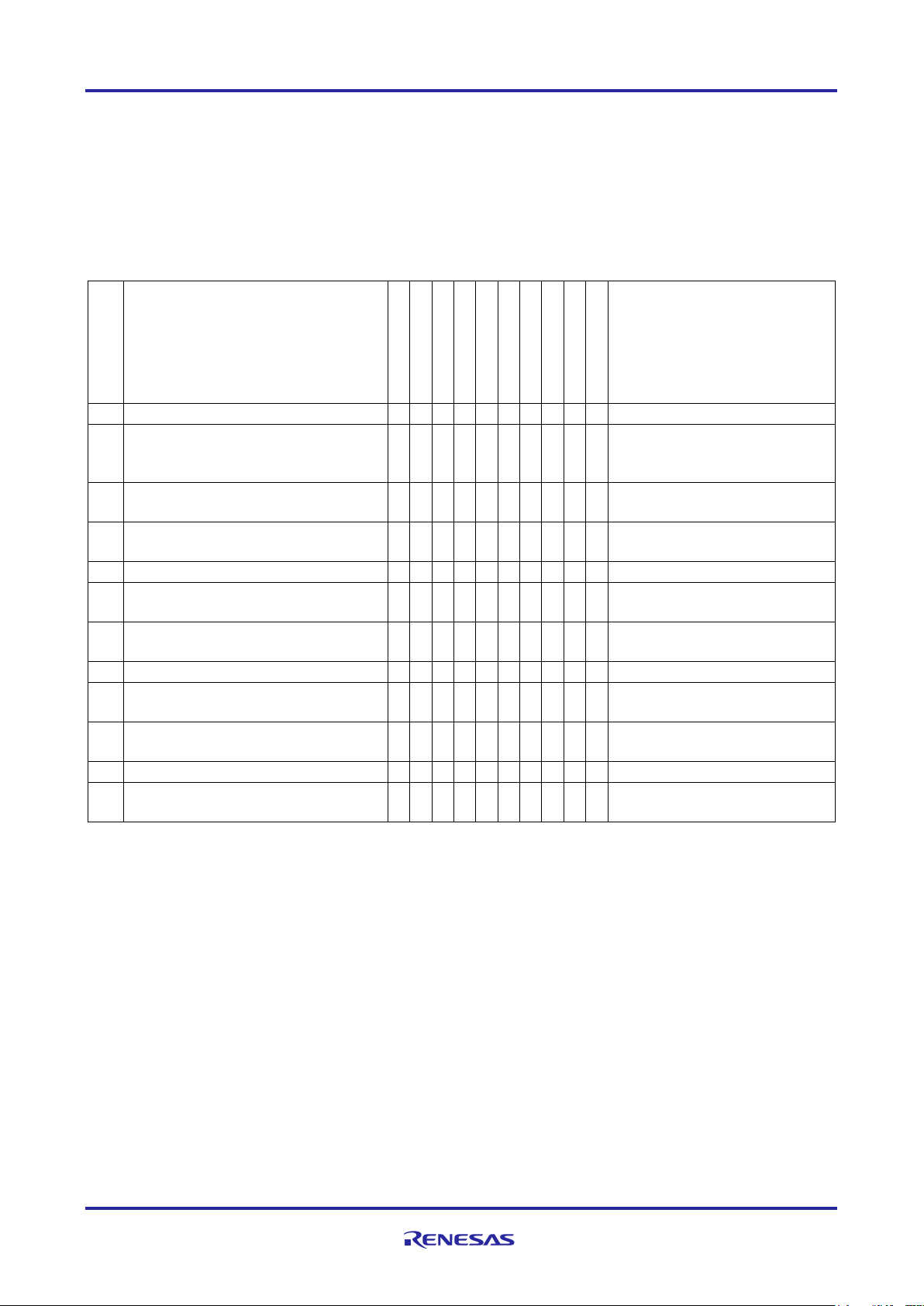
2.1 Support Devices List
Below is a list of devices supported by the Smart Configurator for RX V2.9.1.
Table 2-1 Support Devices
Group
(HW Manual number)
PIN
Device name
RX110 Group
(R01UH0421EJ0120)
36pin
R5F5110HAxLM, R5F5110JAxLM, R5F51101AxLM, R5F51103AxLM
40pin
R5F51101AxNF, R5F51103AxNF, R5F5110HAxNF, R5F5110JAxNF
48pin
R5F51101AxNE, R5F51103AxNE, R5F51104AxNE, R5F51105AxNE,
R5F5110JAxNE, R5F51101AxFL, R5F51103AxFL, R5F51104AxFL,
R5F51105AxFL, R5F5110JAxFL
64pin
R5F51101AxLF, R5F51103AxLF, R5F51104AxLF, R5F51105AxLF,
R5F5110JAxLF, R5F51101AxFK, R5F51103AxFK, R5F51104AxFK,
R5F51105AxFK, R5F5110JAxFK, R5F51101AxFM, R5F51103AxFM,
R5F51104AxFM, R5F51105AxFM, R5F5110JAxFM
RX111 Group
(R01UH0365EJ0130)
36pin
R5F51111AxLM, R5F51113AxLM, R5F5111JAxLM
40pin
R5F51111AxNF, R5F51113AxNF, R5F5111JAxNF
48pin
R5F51111AxFL, R5F51113AxFL, R5F51114AxFL, R5F51115AxFL,
R5F51116AxFL, R5F51117AxFL, R5F51118AxFL, R5F5111JAxFL,
R5F51111AxNE, R5F51113AxNE, R5F51114AxNE, R5F51115AxNE,
R5F51116AxNE, R5F51117AxNE, R5F51118AxNE, R5F5111JAxNE
64pin
R5F51111AxFM, R5F51113AxFM, R5F51114AxFM, R5F51115AxFM,
R5F51116AxFM, R5F51117AxFM, R5F51118AxFM, R5F5111JAxFM,
R5F51111AxFK, R5F51113AxFK, R5F51114AxFK, R5F51115AxFK,
R5F51116AxFK, R5F51117AxFK, R5F51118AxFK, R5F5111JAxFK,
R5F51111AxLF, R5F51113AxLF, R5F51114AxLF, R5F51115AxLF,
R5F51116AxLF, R5F51117AxLF, R5F51118AxLF, R5F5111JAxLF
RX113 Group
(R01UH0448EJ0110)
64pin
R5F51135AxFM, R5F51136AxFM, R5F51137AxFM, R5F51138AxFM
100pin
R5F51135AxLJ, R5F51136AxLJ, R5F51137AxLJ, R5F51138AxLJ,
R5F51135AxFP, R5F51136AxFP, R5F51137AxFP, R5F51138AxFP
RX130 Group
(R01UH0560EJ0200)
48pin
R5F51303AxFL, R5F51305AxFL, R5F51303AxNE, R5F51305AxNE,
R5F51306AxNE, R5F51306AxFL, R5F51307AxNE, R5F51307AxFL,
R5F51308AxNE, R5F51308AxFL, R5F51306BxFL
64pin
R5F51303AxFM, R5F51305AxFM, R5F51303AxFK, R5F51305AxFK,
R5F51306AxFK, R5F51306AxFM, R5F51307AxFK, R5F51307AxFM,
R5F51308AxFK, R5F51308AxFM R5F51308AxFK, R5F51308AxFM,
R5F51306BxFK, R5F51306BxFM
80pin
R5F51303AxFN, R5F51305AxFN, R5F51306AxFN, R5F51306BxFN
100pin
R5F51305AxFP, R5F51306AxFP, R5F51307AxFP, R5F51308AxFP,
R5F51305BxFP, R5F51306BxFP
RX13T Group
(R01UH0822EJ0100)
32pin
R5F513T3AxFJ, R5F513T5AxFJ, R5F513T3AxNH, R5F513T5AxNH
48pin
R5F513T5AxFL, R5F513T3AxFL, R5F513T5AxNE, R5F513T3AxNE
RX230 Group
(R01UH0496EJ0110)
48pin
R5F52305AxNE, R5F52306AxNE, R5F52305AxFL, R5F52306AxFL
64pin
R5F52305AxND, R5F52306AxND, R5F52305AxFM, R5F52306AxFM,
R5F52305AxLF, R5F52306AxLF
100pin
R5F52305AxLA, R5F52306AxLA, R5F52305AxFP, R5F52306AxFP
Page 5
Smart Configurator for RX V2.9.1 Release Note
R20UT4487ES0291 Rev.2.91 Page 5 of 36
Apr.13.21
Table 2-2 Support Devices
Group
(HW Manual number)
PIN
Device name
RX231 Group
(R01UH0496EJ0110)
48pin
R5F52315AxNE, R5F52316AxNE, R5F52317AxNE, R5F52318AxNE,
R5F52315CxNE, R5F52316CxNE, R5F52317BxNE, R5F52318BxNE,
R5F52315AxFL, R5F52316AxFL, R5F52317AxFL, R5F52318AxFL,
R5F52315CxFL, R5F52316CxFL, R5F52317BxFL, R5F52318BxFL
64pin
R5F52315AxND, R5F52316AxND, R5F52317AxND, R5F52318AxND,
R5F52315CxND, R5F52316CxND, R5F52317BxND, R5F52318BxND,
R5F52315AxFM, R5F52316AxFM, R5F52317AxFM, R5F52318AxFM,
R5F52315CxFM, R5F52316CxFM, R5F52317BxFM, R5F52318BxFM,
R5F52315CxLF, R5F52316CxLF
100pin
R5F52315AxLA, R5F52316AxLA, R5F52317AxLA, R5F52318AxLA,
R5F52315CxLA, R5F52316CxLA, R5F52317BxLA, R5F52318BxLA,
R5F52315AxFP, R5F52316AxFP, R5F52317AxFP, R5F52318AxFP,
R5F52315CxFP, R5F52316CxFP, R5F52317BxFP, R5F52318BxFP
RX23E-A Group
(R01UH0801EJ0100)
40pin
R5F523E5AxNF, R5F523E6AxNF, R5F523E5SxNF, R5F523E6SxNF
48pin
R5F523E5AxFL, R5F523E6AxFL, R5F523E5SxFL, R5F523E6SxFL
RX23T Group
(R01UH0520EJ0110)
48pin
R5F523T3AxFL, R5F523T5AxFL
52pin
R5F523T5AxFD, R5F523T3AxFD
64pin
R5F523T5AxFM, R5F523T3AxFM
RX23W Group
(R01UH0823EJ0100)
56pin
R5F523W8BxNG, R5F523W8AxNG, R5F523W7BxNG, R5F523W7AxNG
83pin
R5F523W8CxLN , R5F523W8DxLN
85pin
R5F523W7AxBL, R5F523W8AxBL, R5F523W8BxBL, R5F523W7BxBL
RX24T Group
(R01UH0576EJ0200)
64pin
R5F524TAAxFM, R5F524T8AxFM, R5F524TAAxFK, R5F524T8AxFK
80pin
R5F524TAAxFF, R5F524T8AxFF, R5F524TAAxFN, R5F524T8AxFN
100pin
R5F524TCAxFP, R5F524T8AxFP, R5F524TBAxFP, R5F524TEAxFP,
R5F524TAAxFP
RX24U Group
(R01UH0658EJ0100)
100pin
R5F524UEAxFP, R5F524UCAxFP, R5F524UBAxFP
144pin
R5F524UEAxFB, R5F524UBAxFB, R5F524UCAxFB
RX64M Group
(R01UH0377EJ0110)
100pin
R5F564MFCxFP, R5F564MFCxLJ, R5F564MFDxFP, R5F564MFDxLJ,
R5F564MGCxFP, R5F564MGCxLJ, R5F564MGDxFP, R5F564MGDxLJ,
R5F564MJCxFP, R5F564MJCxLJ, R5F564MJDxFP, R5F564MJDxLJ,
R5F564MLCxFP, R5F564MLCxLJ, R5F564MLDxFP, R5F564MLDxLJ
144/145pin
R5F564MFCxFB, R5F564MFCxLK, R5F564MFDxFB, R5F564MFDxLK,
R5F564MGCxFB, R5F564MGCxLK, R5F564MGDxFB, R5F564MGDxLK,
R5F564MJCxFB, R5F564MJCxLK, R5F564MJDxFB, R5F564MJDxLK,
R5F564MLCxFB, R5F564MLCxLK, R5F564MLDxFB, R5F564MLDxLK
176/177pin
R5F564MFDxFC, R5F564MFDxBG, R5F564MFDxLC, R5F564MFCxFC,
R5F564MFCxBG, R5F564MFCxLC, R5F564MGDxFC, R5F564MGDxBG,
R5F564MGDxLC, R5F564MGCxFC, R5F564MGCxBG, R5F564MGCxLC,
R5F564MJDxFC, R5F564MJDxBG, R5F564MJDxLC, R5F564MJCxFC,
R5F564MJCxBG, R5F564MJCxLC, R5F564MLDxFC, R5F564MLDxBG,
R5F564MLDxLC, R5F564MLCxFC, R5F564MLCxBG, R5F564MLCxLC
Page 6
Smart Configurator for RX V2.9.1 Release Note
R20UT4487ES0291 Rev.2.91 Page 6 of 36
Apr.13.21
Table 2-3 Support Devices
Group
(HW Manual number)
PIN
Device name
RX65N Group
(R01UH0590EJ0210)
100pin
R5F565N9AxLJ, R5F565N9BxLJ, R5F565N9ExLJ, R5F565N9FxLJ,
R5F565N7AxLJ, R5F565N7BxLJ, R5F565N7ExLJ, R5F565N7FxLJ,
R5F565N4AxLJ, R5F565N4BxLJ, R5F565N4ExLJ, R5F565N4FxLJ,
R5F565N9AxFP, R5F565N9BxFP, R5F565N9ExFP, R5F565N9FxFP,
R5F565N7AxFP, R5F565N7BxFP, R5F565N7ExFP, R5F565N7FxFP,
R5F565N4AxFP, R5F565N4BxFP, R5F565N4ExFP, R5F565N4FxFP,
R5F565NCHxLJ, R5F565NCDxLJ, R5F565NEHxLJ, R5F565NEDxLJ,
R5F565NCHxFP, R5F565NCDxFP, R5F565NEHxFP, R5F565NEDxFP
144/145
pin
R5F565N9AxFB, R5F565N9BxFB, R5F565N9ExFB, R5F565N9FxFB,
R5F565N7AxFB, R5F565N7BxFB, R5F565N7ExFB, R5F565N7FxFB,
R5F565N4AxFB, R5F565N4BxFB, R5F565N4ExFB, R5F565N4FxFB,
R5F565NCHxFB, R5F565NCDxFB, R5F565NEHxFB, R5F565NEDxFB,
R5F565N9AxLK, R5F565N9BxLK, R5F565N9ExLK, R5F565N9FxLK,
R5F565N7AxLK, R5F565N7BxLK, R5F565N7ExLK, R5F565N7FxLK,
R5F565N4AxLK, R5F565N4BxLK, R5F565N4ExLK, R5F565N4FxLK,
R5F565NCHxLK, R5F565NCDxLK, R5F565NEHxLK, R5F565NEDxLK
176/177
pin
R5F565NCHxBG, R5F565NCDxBG, R5F565NEHxBG, R5F565NEDxBG,
R5F565NCHxFC, R5F565NCDxFC, R5F565NEHxFC, R5F565NEDxFC,
R5F565NCHxLC, R5F565NCDxLC, R5F565NEHxLC, R5F565NEDxLC
RX651 Group
(R01UH0590EJ0210)
64pin
R5F5651CHxFM,R5F56514FxFM, R5F5651EHxFM, R5F5651CDxFM,
R5F56514FxBP, R5F56514BxFM, R5F56519FxBP, R5F5651CDxBP,
R5F5651EDxBP, R5F5651EDxFM, R5F56517BxBP, R5F5651EHxBP,
R5F56519BxBP, R5F56517FxBP, R5F5651CHxBP, R5F56519FxFM,
R5F56517BxFM, R5F56514BxBP, R5F56519BxFM, R5F56517FxFM
100pin
R5F56519AxLJ, R5F56519BxLJ, R5F56519ExLJ, R5F56519FxLJ,
R5F56517AxLJ, R5F56517BxLJ, R5F56517ExLJ, R5F56517FxLJ,
R5F56514AxLJ, R5F56514BxLJ, R5F56514ExLJ, R5F56514FxLJ,
R5F56519AxFP, R5F56519BxFP, R5F56519ExFP, R5F56519FxFP,
R5F56517AxFP, R5F56517BxFP, R5F56517ExFP, R5F56517FxFP,
R5F56514AxFP, R5F56514BxFP, R5F56514ExFP, R5F56514FxFP
144/145
pin
R5F56519AxFB, R5F56519BxFB, R5F56519ExFB, R5F56519FxFB,
R5F56517AxFB, R5F56517BxFB, R5F56517ExFB, R5F56517FxFB,
R5F56514AxFB, R5F56514BxFB, R5F56514ExFB, R5F56514FxFB,
R5F5651CDxFB, R5F5651CHxFB, R5F5651EDxFB, R5F5651EHxFB,
R5F56519AxLK, R5F56519BxLK, R5F56519ExLK, R5F56519FxLK,
R5F56517AxLK, R5F56517BxLK, R5F56517ExLK, R5F56517FxLK,
R5F56514AxLK, R5F56514BxLK, R5F56514ExLK, R5F56514FxLK,
R5F5651CDxLK, R5F5651CHxLK, R5F5651EDxLK, R5F5651EHxLK
176/177
pin
R5F5651CDxBG, R5F5651CDxFC, R5F5651CHxBG, R5F5651CHxFC,
R5F5651EDxBG, R5F5651EDxFC, R5F5651EHxBG, R5F5651EHxFC,
R5F5651CDxLC, R5F5651CHxLC, R5F5651EDxLC, R5F5651EHxLC
RX66N Group
(R01UH0825EJ0100)
100pin
R5F566NNDxFP, R5F566NNHxFP, R5F566NDDxFP, R5F566NDHxFP
144pin
R5F566NNDxFB, R5F566NNHxFB, R5F566NDDxFB, R5F566NDHxFB
145pin
R5F566NNDxLK, R5F566NNHxLK, R5F566NDDxLK, R5F566NDHxLK
176pin
R5F566NNDxFC, R5F566NNHxFC, R5F566NDDxFC, R5F566NDHxFC,
R5F566NNDxBG, R5F566NNHxBG, R5F566NDDxBG, R5F566NDHxBG
244pin
R5F566NNDxBD, R5F566NNHxBD, R5F566NDDxBD, R5F566NDHxBD
Page 7
Smart Configurator for RX V2.9.1 Release Note
R20UT4487ES0291 Rev.2.91 Page 7 of 36
Apr.13.21
Table 2-4 Support Devices
Group
(HW Manual number)
PIN
Device name
RX66T Group
(R01UH0749EJ0100)
64pin
R5F566TAAxFM, R5F566TAExDFM, R5F566TEAxFM, R5F566TEExFM
80pin
R5F566TAAxFF, R5F566TAExFF, R5F566TEAxFF, R5F566TEExFF,
R5F566TAAxFN, R5F566TAExFN, R5F566TEAxFN, R5F566TEExFN
100pin
R5F566TKCxFP, R5F566TAExFP, R5F566TFFxFP, R5F566TFCxFP,
R5F566TFExFP, R5F566TFBxFP, R5F566TFAxFP, R5F566TABxFP,
R5F566TAFxFP, R5F566TEFxFP, R5F566TKFxFP, R5F566TKGxFP,
R5F566TKAxFP, R5F566TKExFP, R5F566TKBxFP, R5F566TEBxFP,
R5F566TEExFP, R5F566TEAxFP, R5F566TAAxFP, R5F566TFGxFP
112pin
R5F566TAAxFH, R5F566TAExFH, R5F566TEExFH, R5F566TEAxFH
144pin
R5F566TKCxFB, R5F566TFGxFB, R5F566TFCxFB, R5F566TKGxFB
RX71M Group
(R01UH0493EJ0110)
100pin
R5F571MLCxFP, R5F571MLDxFP, R5F571MLGxFP, R5F571MLHxFP,
R5F571MJCxFP, R5F571MJDxFP, R5F571MJGxFP, R5F571MJHxFP,
R5F571MGCxFP, R5F571MGDxFP, R5F571MGGxFP, R5F571MGHxFP,
R5F571MFCxFP, R5F571MFDxFP, R5F571MFGxFP, R5F571MFHxFP,
R5F571MLCxLJ, R5F571MLDxLJ, R5F571MLGxLJ, R5F571MLHxLJ,
R5F571MJCxLJ, R5F571MJDxLJ, R5F571MJGxLJ, R5F571MJHxLJ,
R5F571MGCxLJ, R5F571MGDxLJ, R5F571MGGxLJ, R5F571MGHxLJ,
R5F571MFCxLJ, R5F571MFDxLJ, R5F571MFGxLJ, R5F571MFHxLJ
144/145pin
R5F571MLCxLK, R5F571MLDxLK, R5F571MLGxLK, R5F571MLHxLK,
R5F571MJCxLK, R5F571MJDxLK, R5F571MJGxLK, R5F571MJHxLK,
R5F571MGCxLK, R5F571MGDxLK, R5F571MGGxLK, R5F571MGHxLK,
R5F571MFCxLK, R5F571MFDxLK, R5F571MFGxLK, R5F571MFHxLK,
R5F571MLCxFB, R5F571MLDxFB, R5F571MLGxFB, R5F571MLHxFB,
R5F571MJCxFB, R5F571MJDxFB, R5F571MJGxFB, R5F571MJHxFB,
R5F571MGCxFB, R5F571MGDxFB, R5F571MGGxFB, R5F571MGHxFB,
R5F571MFCxFB, R5F571MFDxFB, R5F571MFGxFB, R5F571MFHxFB
176/177pin
R5F571MLCxFC, R5F571MLDxFC, R5F571MLGxFC, R5F571MLHxFC,
R5F571MJCxFC, R5F571MJDxFC, R5F571MJGxFC, R5F571MJHxFC,
R5F571MGCxFC, R5F571MGDxFC, R5F571MGGxFC, R5F571MGHxFC,
R5F571MFCxFC, R5F571MFDxFC, R5F571MFGxFC, R5F571MFHxFC,
R5F571MLCxLC, R5F571MLDxLC, R5F571MLGxLC, R5F571MLHxLC,
R5F571MJCxLC, R5F571MJDxLC, R5F571MJGxLC, R5F571MJHxLC,
R5F571MGCxLC, R5F571MGDxLC, R5F571MGGxLC, R5F571MGHxLC,
R5F571MFCxLC, R5F571MFDxLC, R5F571MFGxLC, R5F571MFHxLC,
R5F571MLCxBG, R5F571MLDxBG, R5F571MLGxBG, R5F571MLHxBG,
R5F571MJCxBG, R5F571MJDxBG, R5F571MJGxBG, R5F571MJHxBG,
R5F571MGCxBG, R5F571MGDxBG, R5F571MGGxBG, R5F571MGHxBG,
R5F571MFCxBG, R5F571MFDxBG, R5F571MFGxBG, R5F571MFHxBG
RX72M Group
(R01UH0804EJ0110)
100pin
R5F572MDDxFP, R5F572MDHxFP, R5F572MNDxFP, R5F572MNHxFP
144pin
R5F572MDDxFB, R5F572MDHxFB, R5F572MNDxFB, R5F572MNHxFB
176pin
R5F572MNHxFC, R5F572MDDxBG, R5F572MNDxFC, R5F572MDHxBG,
R5F572MDDxFC, R5F572MNHxBG, R5F572MNDxBG, R5F572MDHxFC
224pin
R5F572MDDxBD, R5F572MDHxBD, R5F572MNHxBD, R5F572MNDxBD
Page 8
Smart Configurator for RX V2.9.1 Release Note
R20UT4487ES0291 Rev.2.91 Page 8 of 36
Apr.13.21
Table 2-5 Support Devices
Group
(HW Manual number)
PIN
Device name
RX72N Group
(R01UH0824EJ0100)
100pin
R5F572NNDxFP, R5F572NNHxFP, R5F572NDDxFP, R5F572NDHxFP
144pin
R5F572NNDxFB, R5F572NNHxFB, R5F572NDDxFB, R5F572NDHxFB
145pin
R5F572NNDxLK, R5F572NNHxLK, R5F572NDDxLK, R5F572NDHxLK
176pin
R5F572NNDxFC, R5F572NNHxFC, R5F572NDDxFC, R5F572NDHxFC,
R5F572NNDxBG, R5F572NNHxBG, R5F572NDDxBG, R5F572NDHxBG
224pin
R5F572NNDxBD, R5F572NNHxBD, R5F572NDDxBD, R5F572NDHxBD
RX72T Group
(R01UH0803EJ0100)
100pin
R5F572TKExFP, R5F572TFFxFP, R5F572TKFxFP, R5F572TFGxFP,
R5F572TKCxFP, R5F572TFBxFP, R5F572TFExFP, R5F572TFCxFP,
R5F572TFAxFP, R5F572TKAxFP, R5F572TKBxFP, R5F572TKGxFP
144pin
R5F572TKGxFB, R5F572TKCxFB, R5F572TFGxFB, R5F572TFCxFB
Page 9
Smart Configurator for RX V2.9.1 Release Note
R20UT4487ES0291 Rev.2.91 Page 9 of 36
Apr.13.21
2.2 Support Components List
Below is a list of Components supported by the Smart Configurator for RX V2.9.1.
Table 2-6 Support Components (RX100, RX200 family) ✓: Support, -: Non-
support
No
Components
Mode
RX110
RX111
RX113
RX130
RX13T
RX230, RX231
RX23E-A
RX23T
RX23W
RX24T, RX24U
Remarks
1
8-Bit Timer
- - - ✓ ✓ - ✓ ✓ ✓ ✓ ✓
2
CRC Calculator
- ✓ ✓ ✓ ✓ ✓ ✓ ✓ ✓ ✓ ✓ 3
D-A Converter
- - ✓ ✓ ✓ ✓ ✓ - ✓ ✓ ✓ 4
DMA Controller
- - - - - - ✓ ✓ - ✓ -
5
I2C Slave Mode
I2C mode
✓ ✓ ✓ ✓ ✓ ✓ ✓ ✓ ✓
✓
SMBus mode
✓ ✓ ✓ ✓ ✓ ✓ ✓ ✓ ✓
✓
6
I2C Master Mode
I2C mode
✓ ✓ ✓ ✓ ✓ ✓ ✓ ✓ ✓
✓ SMBus mode
✓ ✓ ✓ ✓ ✓ ✓ ✓ ✓ ✓
✓
7
LCD Controller
- - ✓ - - - - - - -
8
PWM Mode Timer
PWM mode 1
✓ ✓ ✓ ✓ ✓ ✓ ✓ ✓ ✓
✓ PWM mode 2
✓ ✓ ✓ ✓ ✓ ✓ ✓ ✓ ✓
✓
9
SCI/SCIF Clock Synchronous
Mode
Transmission
✓ ✓ ✓ ✓ ✓ ✓ ✓ ✓ ✓
✓
Note 1, 2
Reception
✓ ✓ ✓ ✓ ✓ ✓ ✓ ✓ ✓
✓
Note 1, 2
Transmission/Reception
✓ ✓ ✓ ✓ ✓ ✓ ✓ ✓ ✓
✓
Note 1, 2
10
SCI/SCIF Asynchronous Mode
Transmission
✓ ✓ ✓ ✓ ✓ ✓ ✓ ✓ ✓
✓
Note 1
Reception
✓ ✓ ✓ ✓ ✓ ✓ ✓ ✓ ✓
✓
Note 1
Transmission/Reception
✓ ✓ ✓ ✓ ✓ ✓ ✓ ✓ ✓
✓
Note 1
Multi-processor
Transmission
✓ ✓ ✓ ✓ ✓ ✓ ✓ ✓ ✓
✓
Note 1
Multi-processor Reception
✓ ✓ ✓ ✓ ✓ ✓ ✓ ✓ ✓
✓
Note 1
Multi-processor
Transmission/Reception
✓ ✓ ✓ ✓ ✓ ✓ ✓ ✓ ✓
✓
Note 1
11
SPI Clock Synchronous Mode
Slave transmit/receive
✓ ✓ ✓ ✓ ✓ ✓ ✓ ✓ ✓
✓ Slave transmit only
✓ ✓ ✓ ✓ ✓ ✓ ✓ ✓ ✓
✓
Master transmit/receive
✓ ✓ ✓ ✓ ✓ ✓ ✓ ✓ ✓
✓
Master transmit only
✓ ✓ ✓ ✓ ✓ ✓ ✓ ✓ ✓
✓
12
SPI Operation Mode
Slave transmit/receive
✓ ✓ ✓ ✓ - ✓ ✓ ✓ ✓
✓ Slave transmit only
✓ ✓ ✓ ✓ - ✓ ✓ ✓ ✓
✓ Master transmit/receive
✓ ✓ ✓ ✓ - ✓ ✓ ✓ ✓
✓
Master transmit only
✓ ✓ ✓ ✓ - ✓ ✓ ✓ ✓
✓
Multi-master
transmit/receive
✓ ✓ ✓ ✓ - ✓ ✓ ✓ ✓
✓
Multi-master transmit only
✓ ✓ ✓ ✓ - ✓ ✓ ✓ ✓
✓ 13
Event Link Controller
- - ✓ ✓ ✓ - ✓ ✓ - ✓ -
14
Watchdog Timer
- ✓ ✓ ✓ ✓ - ✓ ✓ ✓ ✓ ✓
15
Clock Frequency Accuracy
Measurement Circuit
- ✓ ✓ ✓ ✓ ✓ ✓ ✓ ✓ ✓ ✓
Note 1. Refer to No 2, 3 in Table 6-2
Note 2. Refer to No 4 in Table 6-2
Page 10
Smart Configurator for RX V2.9.1 Release Note
R20UT4487ES0291 Rev.2.91 Page 10 of 36
Apr.13.21
Table 2-7 Support Components (RX100, RX200 family) ✓: Support, -: Non-support
No
Components
Mode
RX110
RX111
RX113
RX130
RX13T
RX230, RX231
RX23E-A
RX23T
RX23W
RX24T, RX24U
Remarks
16
Group Scan Mode S12AD
- ✓ ✓ ✓ ✓ ✓ ✓ ✓ ✓ ✓ ✓
17
Comparator
- - - ✓ ✓ ✓ ✓ - - ✓ - 18
Compare Match Timer
- ✓ ✓ ✓ ✓ ✓ ✓ ✓ ✓ ✓ ✓
19
Single Scan Mode S12AD
- ✓ ✓ ✓ ✓ ✓ ✓ ✓ ✓ ✓ ✓
20
Smart Card Interface Mode
Transmission
✓ ✓ ✓ ✓ ✓ ✓ ✓ ✓ ✓
✓
Reception
✓ ✓ ✓ ✓ ✓ ✓ ✓ ✓ ✓
✓ Transmission/Reception
✓ ✓ ✓ ✓ ✓ ✓ ✓ ✓ ✓
✓
21
Dead-time Compensation
Counter
- ✓ ✓ ✓ ✓ ✓ ✓ ✓ ✓ - ✓
22
Data Transfer Controller
- ✓ ✓ ✓ ✓ ✓ ✓ ✓ ✓ ✓ ✓
Note 3
23
Data Operation Circuit
- ✓ ✓ ✓ ✓ ✓ ✓ ✓ ✓ ✓ ✓ 24
Normal Mode Timer
✓ ✓ ✓ ✓ ✓ ✓ ✓ ✓ ✓ ✓ 25
Buses
- ✓ ✓ ✓ ✓ ✓ ✓ ✓ ✓ ✓ ✓
26
Programmable Pulse
Generator
- - - - - - - - - - 27
Ports
- ✓ ✓ ✓ ✓ ✓ ✓ ✓ ✓ ✓ ✓ 28
Port Output Enable
- - ✓ ✓ ✓ ✓ ✓ ✓ ✓ ✓ ✓
29
Real Time Clock
Binary
✓ ✓ ✓ ✓ - ✓ - - ✓
-
Calendar
✓ ✓ ✓ ✓ - ✓ - - ✓
-
30
Remote Control Signal
Receiver
- - - - ✓ - - - - - 31
Low-Power Timer
- - - ✓ ✓ - ✓ ✓ - ✓ -
32
Phase Counting Mode Timer
16-Bit Phase Counting Mode
✓ ✓ ✓ ✓ ✓ ✓ ✓ ✓ ✓
✓
Cascade Connection 32-Bit
Phase Counting Mode
- - - - ✓ - - ✓ -
✓
33
Interrupt Controller
- ✓ ✓ ✓ ✓ ✓ ✓ ✓ ✓ ✓ ✓
34
General PWM Timer
Saw-wave PWM mode
- - - - - - - ✓ -
✓
Note 4
Saw-wave one-shot pulse
mode
- - - - - - - ✓ -
✓
Note 4
Triangle-wave PWM mode 1
- - - - - - - ✓ -
✓
Note 4
Triangle-wave PWM mode 2
- - - - - - - ✓ -
✓
Note 4
Triangle-wave PWM mode 3
- - - - - - - ✓ -
✓
Note 4
35
Low Power Consumption
- ✓ ✓ ✓ ✓ ✓ ✓ ✓ ✓ ✓ ✓
36
Complementary PWM Mode
Timer
Complementary PWM mode 1
- ✓ ✓ ✓ ✓ ✓ ✓ ✓ ✓
✓
Complementary PWM mode 2
- ✓ ✓ ✓ ✓ ✓ ✓ ✓ ✓
✓
Complementary PWM mode 3
- ✓ ✓ ✓ ✓ ✓ ✓ ✓ ✓
✓
37
Continuous Scan Mode S12AD
- ✓ ✓ ✓ ✓ ✓ ✓ ✓ ✓ ✓ ✓
Note 3. Refer to No 8 in Table 6-1
Note 4. Refer to No 1 in Table 6-1
Page 11
Smart Configurator for RX V2.9.1 Release Note
R20UT4487ES0291 Rev.2.91 Page 11 of 36
Apr.13.21
Table 2-8 Support Components (RX100, RX200 family) ✓: Support, -: Non-support
No
Components
Mode
RX110
RX111
RX113
RX130
RX13T
RX230, RX231
RX23E-A
RX23T
RX23W
RX24T, RX24U
Remarks
38
Voltage Detection Circuit
- ✓ ✓ ✓ ✓ ✓ ✓ ✓ ✓ ✓ ✓
39
Delta-Sigma Modulator
Interface
Master
- - - - - - - - -
- Slave
- - - - - - - - -
-
40
Single Scan Mode DSAD
- - - - - - - ✓ - - -
41
Continuous Scan Mode DSAD
- - - - - - - ✓ - - - 42
Analog Front End
- - - - - - - ✓ - - -
43
Motor
3-Phase Brushless DC
Motor
- - - - ✓ - - ✓ -
✓ 2-Phase Stepping Motor
(Fast Decay)
- - - - ✓ - - ✓ -
✓ 2-Phase Stepping Motor
(Slow Decay)
- - - - ✓ - - ✓ -
✓
Page 12
Smart Configurator for RX V2.9.1 Release Note
R20UT4487ES0291 Rev.2.91 Page 12 of 36
Apr.13.21
Table 2-9 Support Components (RX600, RX700 family) ✓: Support, -: Non-support
No
Components
Mode
RX64M
RX65N, RX651
RX66N
RX66T
RX71M
RX72M
RX72N
RX72T
Remarks
1
8-Bit Timer
- ✓ ✓ ✓ ✓ ✓ ✓ ✓ ✓ 2
CRC Calculator
- ✓ ✓ ✓ ✓ ✓ ✓ ✓ ✓ 3
D/A Converter
- ✓ ✓ ✓ ✓ ✓ ✓ ✓ ✓
4
DMA Controller
- ✓ ✓ ✓ ✓ ✓ ✓ ✓ ✓
5
I2C Slave Mode
I2C mode
✓ ✓ ✓ ✓ ✓ ✓ ✓
✓ SMBus mode
✓ ✓ ✓ ✓ ✓ ✓ ✓
✓
6
I2C Master Mode
I2C mode
✓ ✓ ✓ ✓ ✓ ✓ ✓
✓
SMBus mode
✓ ✓ ✓ ✓ ✓ ✓ ✓
✓
7
LCD Controller
- - - - - - - - -
8
PWM Mode Timer
PWM mode 1
✓ ✓ ✓ ✓ ✓ ✓ ✓
✓
PWM mode 2
✓ ✓ ✓ ✓ ✓ ✓ ✓
✓
9
SCI/SCIF Clock Synchronous
Mode
Transmission
✓ ✓ ✓ ✓ ✓ ✓ ✓
✓
Note 1, 2
Reception
✓ ✓ ✓ ✓ ✓ ✓ ✓
✓
Note 1, 2
Transmission/Reception
✓ ✓ ✓ ✓ ✓ ✓ ✓
✓
Note 1, 2
10
SCI/SCIF Asynchronous Mode
Transmission
✓ ✓ ✓ ✓ ✓ ✓ ✓
✓
Note 1
Reception
✓ ✓ ✓ ✓ ✓ ✓ ✓
✓
Note 1
Transmission/Reception
✓ ✓ ✓ ✓ ✓ ✓ ✓
✓
Note 1
Multi-processor
Transmission
✓ ✓ ✓ ✓ ✓ ✓ ✓
✓
Note 1
Multi-processor Reception
✓ ✓ ✓ ✓ ✓ ✓ ✓
✓
Note 1
Multi-processor
Transmission/Reception
✓ ✓ ✓ ✓ ✓ ✓ ✓
✓
Note 1
11
SPI Clock Synchronous Mode
Slave transmit/receive
✓ ✓ ✓ ✓ ✓ ✓ ✓
✓ Slave transmit only
✓ ✓ ✓ ✓ ✓ ✓ ✓
✓
Master transmit/receive
✓ ✓ ✓ ✓ ✓ ✓ ✓
✓
Master transmit only
✓ ✓ ✓ ✓ ✓ ✓ ✓
✓
12
SPI Operation Mode
Slave transmit/receive
✓ ✓ ✓ ✓ ✓ ✓ ✓
✓ Slave transmit only
✓ ✓ ✓ ✓ ✓ ✓ ✓
✓
Master transmit/receive
✓ ✓ ✓ ✓ ✓ ✓ ✓
✓
Master transmit only
✓ ✓ ✓ ✓ ✓ ✓ ✓
✓
Multi-master
transmit/receive
✓ ✓ ✓ ✓ ✓ ✓ ✓
✓
Multi-master transmit only
✓ ✓ ✓ ✓ ✓ ✓ ✓
✓
13
Event Link Controller
- ✓ ✓ ✓ ✓ ✓ ✓ ✓ ✓
14
Watchdog Timer
- ✓ ✓ ✓ ✓ ✓ ✓ ✓ ✓
15
Clock Frequency Accuracy
Measurement Circuit
- ✓ ✓ ✓ ✓ ✓ ✓ ✓ ✓
Note 1. Refer to No 2, 3 in Table 6-2
Note 2. Refer to No 4 in Table 6-2
Page 13

Smart Configurator for RX V2.9.1 Release Note
R20UT4487ES0291 Rev.2.91 Page 13 of 36
Apr.13.21
Table 2-10 Support Components (RX600, RX700 family) ✓: Support, -: Non-support
No
Components
Mode
RX64M
RX65N, RX651
RX66N
RX66T
RX71M
RX72M
RX72N
RX72T
Remarks
16
Group Scan Mode S12AD
- ✓ ✓ ✓ ✓ ✓ ✓ ✓ ✓
17
Comparator
- - - - ✓ - ✓ - ✓ 18
Compare Match Timer
- ✓ ✓ ✓ ✓ ✓ ✓ ✓ ✓
19
Single Scan Mode S12AD
- ✓ ✓ ✓ ✓ ✓ ✓ ✓ ✓
20
Smart Card Interface Mode
Transmission
✓ ✓ ✓ ✓ ✓ ✓ ✓
✓
Reception
✓ ✓ ✓ ✓ ✓ ✓ ✓
✓ Transmission/Reception
✓ ✓ ✓ ✓ ✓ ✓ ✓
✓
21
Dead-time Compensation
Counter
- ✓ ✓ ✓ ✓ ✓ ✓ ✓ ✓
22
Data Transfer Controller
- ✓ ✓ ✓ ✓ ✓ ✓ ✓ ✓
Note 3
23
Data Operation Circuit
- ✓ ✓ ✓ ✓ ✓ ✓ ✓ ✓ 24
Normal Mode Timer
✓ ✓ ✓ ✓ ✓ ✓ ✓ ✓ 25
Buses
- ✓ ✓ ✓ ✓ ✓ ✓ ✓ ✓
26
Programmable Pulse
Generator
- ✓ ✓ ✓ - ✓ - ✓ 27
Ports
- ✓ ✓ ✓ ✓ ✓ ✓ ✓ ✓ 28
Port Output Enable
- ✓ ✓ ✓ ✓ ✓ ✓ ✓ ✓
29
Real Time Clock
Binary
✓ ✓ ✓ - ✓ - ✓
-
Calendar
✓ ✓ ✓ - ✓ - ✓
-
30
Remote Control Signal
Receiver
- - - - - - - - 31
Low-Power Timer
- - - - - - - - -
32
Phase Counting Mode Timer
16-Bit Phase Counting Mode
✓ ✓ ✓ ✓ ✓ ✓ ✓
✓
Cascade Connection 32-Bit Phase
Counting Mode
✓ ✓ ✓ ✓ ✓ ✓ ✓
✓
33
Interrupt Controller
- ✓ ✓ ✓ ✓ ✓ ✓ ✓ ✓
34
General PWM Timer
Saw-wave PWM mode
✓ - ✓ ✓ ✓ ✓ ✓
✓
Note 4
Saw-wave one-shot pulse mode
✓ - ✓ ✓ ✓ ✓ ✓
✓
Note 4
Triangle-wave PWM mode 1
✓ - ✓ ✓ ✓ ✓ ✓
✓
Note 4
Triangle-wave PWM mode 2
✓ - ✓ ✓ ✓ ✓ ✓
✓
Note 4
Triangle-wave PWM mode 3
✓ - ✓ ✓ ✓ ✓ ✓
✓
Note 4
35
Low Power Consumption
- ✓ ✓ ✓ ✓ ✓ ✓ ✓ ✓
36
Complementary PWM Mode
Timer
Complementary PWM mode 1
✓ ✓ ✓ ✓ ✓ ✓ ✓
✓
Complementary PWM mode 2
✓ ✓ ✓ ✓ ✓ ✓ ✓
✓
Complementary PWM mode 3
✓ ✓ ✓ ✓ ✓ ✓ ✓
✓
37
Continuous Scan Mode
S12AD
- ✓ ✓ ✓ ✓ ✓ ✓ ✓ ✓
Note 3. Refer to No 8 in Table 6-1
Note 4. Refer to No 1 in Table 6-1
Page 14

Smart Configurator for RX V2.9.1 Release Note
R20UT4487ES0291 Rev.2.91 Page 14 of 36
Apr.13.21
Table 2-11 Support Components (RX600, RX700 family) ✓: Support, -: Non-support
No
Components
Mode
RX64M
RX65N, RX651
RX66N
RX66T
RX71M
RX72M
RX72N
RX72T
Remarks
38
Voltage Detection Circuit
- ✓ ✓ ✓ ✓ ✓ ✓ ✓ ✓
39
Delta-Sigma Modulator
Interface
Master
- - - - - ✓ -
- Slave
- - - - - ✓ -
- 40
Single Scan Mode DSAD
- - - - - - - - -
41
Continuous Scan Mode DSAD
- - - - - - - - -
42
Analog Front End
- - - - - - - - -
43
Motor
3-Phase Brushless DC
Motor
- - - ✓ - ✓ -
✓
2-Phase Stepping Motor
(Fast Decay)
- - - ✓ - ✓ -
✓
2-Phase Stepping Motor
(Slow Decay)
- - - ✓ - ✓ -
✓
Page 15

Smart Configurator for RX V2.9.1 Release Note
R20UT4487ES0291 Rev.2.91 Page 15 of 36
Apr.13.21
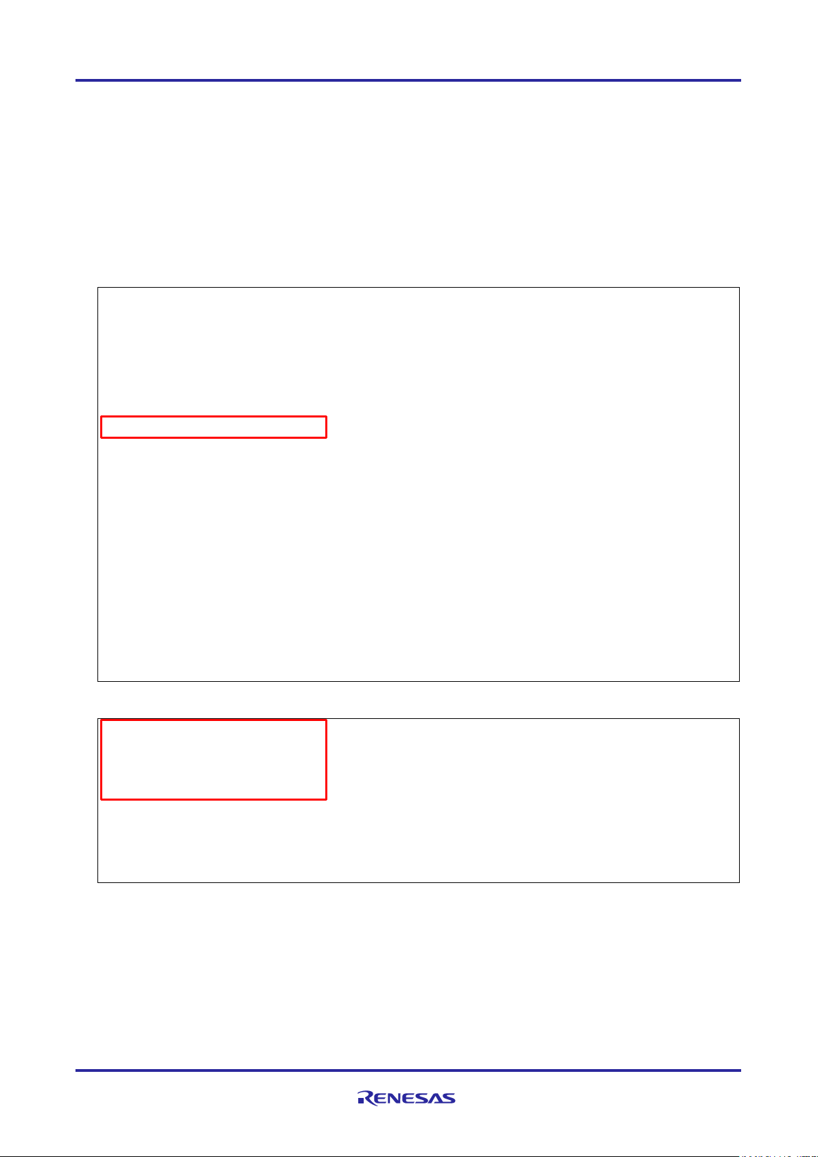
2.3 New support
2.3.1 BSP (Board Support Package) revision update
From Smart Configurator for RX V2.9.1, BSP rev5.64 is supported and will be added as default BSP
when creating Smart Configurator project.
2.3.2 Toolbar icons update
From Smart Configurator for RX V2.9.1, bigger toolbar icons for "Generate Code" and "Generate Report"
functions are applied as below.
Figure 2-1: New icons for “Generate Code” and “Generate Report” functions
2.3.3 Software component version number has been added into report
From Smart Configurator for RX V2.9.1, software component version number has been added into the
generated report, e.g. BSP (Board Support Package) component version number as below:
Figure 2-2: BSP software component version number in generated report
Page 16

Smart Configurator for RX V2.9.1 Release Note
R20UT4487ES0291 Rev.2.91 Page 16 of 36
Apr.13.21
2.3.4 Generated source files’ folder can be accessed from console window
From Smart Configurator for RX V2.9.1, the root folder path for the generated source files has been
outputted to console window after code generation, and user can open this folder directly by just clicking
its hyperlink.
Figure 2-3: Root folder path for the generated source files
Page 17

Smart Configurator for RX V2.9.1 Release Note
R20UT4487ES0291 Rev.2.91 Page 17 of 36
Apr.13.21
3. Changes
This chapter describes changes to the Smart Configurator for RX V2.9.1.
3.1 Correction of issues/limitations
Table 3-1 List of Correction of issues/limitations (RX100, RX200 Family) ✓: Applicable, -: Not Applicable
No
Description
RX110
RX111
RX113
RX130
RX13T
RX230, RX231
RX23E-A
RX23T
RX23W
RX24T, RX24U
Remarks
1
Fixed the pin codes missing issue when using MTU
components
-
- - - ✓ - - ✓ - ✓
2 Fixed the resource change issue when using MTU
Normal Mode Timer Component
-
- - - - - - - - -
3
Fixed the device change issue when using BSP rev5.63
✓
✓ ✓ ✓ ✓ ✓ ✓ ✓ ✓ ✓
4
Fixed the generated codes’ folder issue for FreeRTOS
(with IoT libraries) project
✓ ✓ ✓ ✓ ✓ ✓ ✓ ✓ ✓
✓
5
Fixed the interrupt migration report status issue when
performing the device change without opening Smart
Configurator GUI
✓ ✓ ✓ ✓ ✓ ✓ ✓ ✓ ✓
✓
6
Fixed the configurable issue for PH7 when using PORT
component
✓ ✓ ✓ - - - - - -
-
Table 3-2 List of Correction of issues/limitations (RX600, RX700 Family) ✓: Applicable, -: Not Applicable
No
Description
RX64M
RX65N, RX651
RX66N
RX66T
RX71M
RX72M
RX72N
RX72T
Remarks
1
Fixed the pin codes missing issue when using
MTU components
✓ ✓ ✓ ✓ ✓ ✓ ✓
✓
2 Fixed the resource change issue when using
MTU Normal Mode Timer Component
✓ ✓ - - ✓ ✓ ✓
-
3
Fixed the device change issue when using BSP
rev5.63
✓ ✓ ✓ ✓ ✓ ✓ ✓
✓
4
Fixed the generated codes’ folder issue for
FreeRTOS (with IoT libraries) project
✓ ✓ ✓ ✓ ✓ ✓ ✓
✓
5
Fixed the interrupt migration report status issue
when performing the device change without
opening Smart Configurator GUI
✓ ✓ ✓ ✓ ✓ ✓ ✓
✓
6
Fixed the configurable issue for PH7 when using
PORT component
- - - - - - -
-
Page 18

Smart Configurator for RX V2.9.1 Release Note
R20UT4487ES0291 Rev.2.91 Page 18 of 36
Apr.13.21
3.1.1 Fixed the pin codes missing issue when using MTU components
When using MTU components as below, if set MTIOC1A pin as external clock source input for
MTU0/MTU5 counter, MTIOC1A pin codes will not be generated out as expected in the MTU0/MTU5
initialization codes, this issue has been fixed from SC for RX V2.9.1
• Normal Mode Timer component
• PWM Mode Timer component
• Dead-time Compensation Counter component
• Phase Counting Mode Timer component
3.1.2 Fixed the resource change issue when using MTU Normal Mode Timer Component
When using MTU Normal Mode Timer Component, If a resource change is performed from any channel
with synchronous mode setting to MTU8, synchronous mode setting will be ported over to MTU8 and
corresponding codes will be generated out, this is unexpected because MTU8 doesn't support
synchronous mode setting, this issue has been fixed from SC for RX V2.9.1
3.1.3 Fixed the device change issue when using BSP rev5.63
When using BSP rev5.63 and perform device change operation, the configuration nodes for all existing
components will be removed from software component tree after device change if the source device’s
SCI channels are more than the destination device’s SCI channels, this issue has been fixed from SC for
RX V2.9.1
3.1.4 Fixed the generated codes’ folder issue for FreeRTOS (with IoT libraries) project
When using Smart Configurator for FreeRTOS (with loT libraries) project, if user changes the source
codes generated location to another new path on the Overview page and clicks “Generate code” button,
the previous generated codes’ folder (e.g. ‘smc_gen’) is not removed automatically, user needs to delete
it manually to avoid build errors, this issue has been fixed from SC for RX V2.9.1
3.1.5 Fixed the interrupt migration report status issue when performing the device change
without opening Smart Configurator GUI
When performing the device change without opening Smart Configurator GUI, interrupt migration status is
incorrect in the migration report for interrupts that are available on source device but not available on the
destination device, this issue has been fixed from SC for RX V2.9.1
3.1.6 Fixed the configurable issue for PH7 when using PORT component
When using PORT component, the PH7 is still configurable for input usage on the PORT GUI, but it is not
allowed according to technical update TN-RX*-A180A/E (please find more details from Chapter 4 table
list), this issue has been fixed from SC for RX V2.9.1
Page 19

Smart Configurator for RX V2.9.1 Release Note
R20UT4487ES0291 Rev.2.91 Page 19 of 36
Apr.13.21
3.2 Specification changes
Table 3-3 List of Specification changes (RX100, RX200 family) ○: Applicable, /: Not Applicable
No
Description
RX110
RX111
RX113
RX130
RX13T
RX230, RX231
RX23E-A
RX23T
RX23W
RX24T, RX24U
Remarks
1
Improved the Import and Export function layouts
for the Board and Pins pages
✓ ✓ ✓ ✓ ✓ ✓ ✓ ✓ ✓
✓
2
Drop-down list items of the “Function” selection
combo box for the New Component dialog are
tidied up
✓ ✓ ✓ ✓ ✓ ✓ ✓ ✓ ✓
✓
Table 3-4 List of Specification changes (RX600, RX700 family) ○: Applicable, /: Not Applicable
No
Description
RX64M
RX65N, RX651
RX66N
RX66T
RX71M
RX72M
RX72N
RX72T
Remarks
1
Improved the Import and Export function layouts for the
Board and Pins pages
✓ ✓ ✓ ✓ ✓ ✓ ✓
✓
2
Drop-down list items of the “Function” selection combo
box for the New Component dialog are tidied up
✓ ✓ ✓ ✓ ✓ ✓ ✓
✓
Page 20

Smart Configurator for RX V2.9.1 Release Note
R20UT4487ES0291 Rev.2.91 Page 20 of 36
Apr.13.21
3.2.1 Improved the Import and Export function layouts for the Board and Pins pages
From Smart Configurator RX V2.9.1, layouts have been improved for the Import and Export function on
the Board and Pins pages.
• An Import Board settings dialog box has been added after clicking the “Import” button on Board
page
Figure 3-1: New Import Board Settings dialog for Board page
• An Import Pin assignments dialog box has been added after clicking the “Import” button on Pins
page
Figure 3-2: New Import Pin Assignments dialog for Pins page
Page 21
Smart Configurator for RX V2.9.1 Release Note
R20UT4487ES0291 Rev.2.91 Page 21 of 36
Apr.13.21
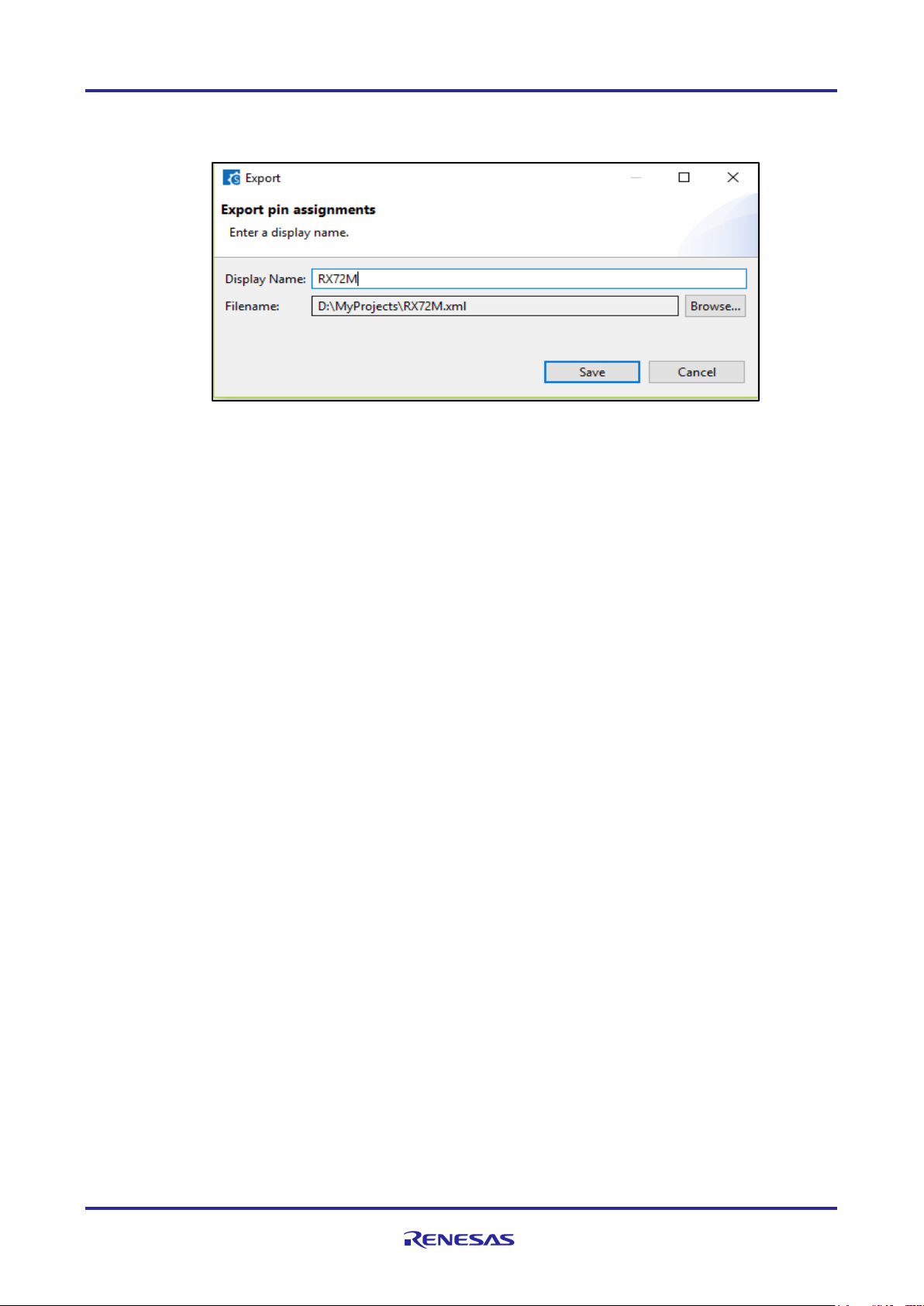
• An Export Pin assignments dialog box has been added after clicking the “Export” button on Pins
page
Figure 3-3: New Export Pin Assignments dialog for Pins page
3.2.2 Drop-down list items of the “Function” selection combo box for the New Component dialog are tidied up
From Smart Configurator RX V2.9.1, drop-down list items of the “Function” selection combo box for the
New Component dialog are tidied up, some unused categories (e.g. “Generic” and “Graphic” categories)
and unnecessary category information have been removed.
Page 22

Smart Configurator for RX V2.9.1 Release Note
R20UT4487ES0291 Rev.2.91 Page 22 of 36
Apr.13.21
4. List of RENESAS TOOL NEWS AND TECHNICAL UPDATE
Below is a list of notifications delivered by RENESAS TOOL NEWS and TECHNICAL UPDATE.
Issue date
Document No.
Description
Applicable
MCUs
Fixed
version
Sep. 1, 2017
R20TS0198
1. When using the I2C bus interface in
slave mode
https://www.renesas.com/document/tnn/
notes-e-studio-smart-configurator-plugsmart-configurator-rx
RX130,
RX64M,
RX651,
RX65N
V1.3.0
Apr. 1, 2018
R20TS0294
1. When using the bus for peripheral
functions
https://www.renesas.com/document/tnn/
notes-cs-smart-configurator-rx-e-studiosmart-configurator-plug
RX230,
RX231
V1.4.0
Oct. 01, 2018
R20TS0351
1. Setting TPU0 channel of PWM Mode
Timer
https://www.renesas.com/document/tnn/
notes-e-studio-smart-configurator-plugsmart-configurator-rx-0
RX65N,
RX651,
RX64M
V1.5.0
Feb.01, 2019
R20TS0401
1. Point for caution when using the
GTIOCnm pin (n = 0 to 9, m = A, B) of the
general PWM timer (GPTW) as a
hardware source
https://www.renesas.com/document/tnn/
notes-e-studio-smart-configurator-plugsmart-configurator-rx-1
RX66T
V2.1.0
Apr.16, 2019
R20TS0425
1. When using the I2C bus interface in
master mode
https://www.renesas.com/document/tnn/
notes-e-studio-smart-configurator-plugsmart-configurator-rx-2
RX110,
RX111,
RX113,
RX130,
RX230,
RX231,
RX23T,
RX24T,
RX24U,
RX64M,
RX651,
RX65N,
RX71M
V2.2.0
Jun.01, 2019
R20TS0434
1. When using self-diagnosis function of
12-bit A/D converter in Single Scan
Mode
2. When using Serial Peripheral
Interface clock synchronous mode in
slave transmit
3. When using I2C Bus Interface with
Fast-mode Plus enabled
https://www.renesas.com/document/tnn/
notes-e-studio-smart-configurator-plugsmart-configurator-rx-3
RX230,
RX231,
RX66T,
RX72T,
RX64M,
RX651,
RX65N,
RX71M
V2.2.0
Page 23

Smart Configurator for RX V2.9.1 Release Note
R20UT4487ES0291 Rev.2.91 Page 23 of 36
Apr.13.21
Issue date
Document No.
Description
Applicable
MCUs
Fixed
version
Jun.16, 2019
R20TS0436
1. When using general PWM timer
https://www.renesas.com/document/tnn/
notes-e-studio-smart-configurator-plug-
smart-configurator-rx-4
RX66T,
RX72T
V2.2.0
Aug.01, 2019
R20TS0466
1. When using the NACK reception
transfer suspension function on the I²C
bus interface
https://www.renesas.com/document/tnn/
notes-e-studio-smart-configurator-plugsmart-configurator-rx-5
RX110,
RX111,
RX113,
RX130,
RX230,
RX231,
RX23T,
RX24T,
RX24U,
RX64M,
RX651,
RX65N,
RX66T,
RX71M,
RX72M,
RX72T
V2.3.0
Sep.16, 2019
R20TS0477
1. When Using the Automatic Adjustment
Function for Time Error Adjustment on
the Realtime Clock
https://www.renesas.com/document/tnn/
notes-e-studio-smart-configurator-plugsmart-configurator-rx-6
RX110,
RX111,
RX113,
RX130,
RX230,
RX231,
RX64M,
RX651,
RX65N
V2.4.0
Dec.16, 2019
R20TS0522
1. When using temperature sensor
output or internal reference voltage for
comparison function on S12AD
components (Single Scan Mode, Group
Scan Mode and Continuous Scan Mode)
2. When using calendar mode API to set
counter value on RTC component
3. When using window B for comparison
function on S12AD Continuous Scan
Mode component
4. When using double trigger mode on
S12AD Single Scan Mode component
https://www.renesas.com/document/tnn/
notes-e-studio-smart-configurator-plugsmart-configurator-rx-7
RX64M,
RX651,
RX65N,
RX66T,
RX71M,
RX72M,
RX72T
V2.4.0
Feb. 01, 2020
R20TS0546
1. When using the PLL frequency
synthesizer of the clock
https://www.renesas.com/document/tnn/
notes-e-studio-smart-configurator-plugsmart-configurator-rx-8
RX64M,
RX651,
RX65N,
RX66T,
RX71M,
RX72T
V2.5.0
Page 24
Smart Configurator for RX V2.9.1 Release Note
R20UT4487ES0291 Rev.2.91 Page 24 of 36
Apr.13.21
Issue date
Document No.
Description
Applicable
MCUs
Fixed
version
Mar. 16, 2020
R20TS0555
1. When using the TGIC7 and TGID7
interrupts in Normal Mode Timer or
PWM Mode Timer
2. When creating a project with RX24T
64-pin FK packages
3. When using compare level of AN109
in Single Scan Mode S12AD
https://www.renesas.com/document/tnn/
notes-e-studio-smart-configurator-plugsmart-configurator-rx-9
RX24T,
RX24U,
RX71M
V2.5.0
Apr.03, 2020
TN-RX*-A0222
Errata to RX72N Group User’s Manual:
Hardware Rev.1.00
https://www.renesas.com/document/tcu/errat
a-rx72n-group-users-manual-hardwarerev100
RX72N
V2.5.0
May.16, 2020
R20TS0579
1. When using Stop API in Continuous
Scan Mode DSAD and Single Scan
Mode DSAD components
https://www.renesas.com/document/tnn/
notes-e-studio-smart-configurator-plugsmart-configurator-rx-10
RX23E-A
V2.6.0
Jun.16, 2020
R20TS0591
1. When using Data Transfer Controller
(DTC) component and making
configuration for its vector base address
2. When using SCI/SCIF Asynchronous
Mode component and making
configuration for its bit-rate
3. When using AN007 or AN107 as
analog input pins in S12AD components
https://www.renesas.com/document/tnn/
notes-e-studio-smart-configurator-plugsmart-configurator-rx-11
RX230,
RX231,
RX651,
RX65N,
RX66T,
RX72T
V2.6.0
Aug. 21, 2020
TN-RX*-A0234A/E
Errata to the RX113 Group User’s
Manual: Hardware Rev.1.10
https://www.renesas.com/document/tcu/
errata-rx113-group-users-manualhardware
RX113
V2.8.0
Sep. 01, 2020
R20TS0611
When using PWM Mode component and
making configuration with MTU channel
1 and 2
https://www.renesas.com/document/tnn/
notes-e-studio-smart-configurator-plugsmart-configurator-rx-13
RX13T,
RX23T,
RX24T,
RX24U
V2.7.0
Page 25

Smart Configurator for RX V2.9.1 Release Note
R20UT4487ES0291 Rev.2.91 Page 25 of 36
Apr.13.21
Issue date
Document No.
Description
Applicable
MCUs
Fixed
version
Sep. 24, 2020
TN-RX*-A0235B/E
Notes on the Transmit Data Empty
Interrupt When the FIFO is in Use with
the Serial Communications Interface
(SCI)
https://www.renesas.com/document/tcu/
notes-transmit-data-empty-interruptwhen-fifo-use-serial-communicationsinterface-sci
RX651,
RX65N,
RX66N,
RX66T,
RX72M,
RX72N,
RX72T
V2.7.0
Oct. 01, 2020
R20TS0623
1. When using “r_sci_rx” component and
making pin configurations for RXD and
TXD
2. When using “r_sci_rx” component,
duplicate SCI11 channels are displayed
in the Components configuration panel
https://www.renesas.com/document/tnn/
notes-e-studio-smart-configurator-plugsmart-configurator-rx-12
RX651,
RX65N,
RX66N,
RX72M,
RX72N
V2.7.0
Dec. 01, 2020
R20TS0638
1. Note on setting timer operation period
in Motor component.
2. When loading project with port
configuration created in V2.5.0 or
version before into V2.6.0 version
onwards
https://www.renesas.com/document/tnn/
notes-e-studio-smart-configurator-plugsmart-configurator-rx-14
RX13T,
RX23T,
RX24T,
RX24U,
RX651,
RX65N,
RX66T,
RX72T,
RX72M
V2.8.0
Aug. 29, 2017
TN-RX*-A180A/E
Restriction for the PH7/XCIN Pin
https://www.renesas.com/document/tcu/
restriction-ph7xcin-pin
RX110,
RX111,
RX113
V2.9.1
Page 26
Smart Configurator for RX V2.9.1 Release Note
R20UT4487ES0291 Rev.2.91 Page 26 of 36
Apr.13.21
5. Points for Limitation
Below is a list of notifications delivered by RENESAS TOOL NEWS and TECHNICAL UPDATE.
5.1 List of Limitation
Table 5-1 List of Correction of issues/limitations (RX100, RX200 Family) ✓: Applicable, -: Not Applicable
No
Description
RX110
RX111
RX113
RX130
RX13T
RX230, RX231
RX23E-A
RX23T
RX23W
RX24T, RX24U
Remarks
1
Note on the inconsistent code generation behavior issue
when loading existing project with Port configuration
✓ ✓ ✓ ✓ - ✓ - - - -
2
Note on general I/O port direction issue on MCU
package view when using Port Component
✓ ✓ ✓ ✓ ✓ ✓ ✓ ✓ ✓ ✓
3
Note on CLKOUT pin settings on the clock page
✓ ✓ ✓ ✓ - ✓ - - - -
4
Note on the resource tree in the FIT component GUI
configuration
✓ ✓ ✓ ✓ ✓ ✓ ✓ ✓ ✓ ✓
5
Note on address pin when using external bus
- - - - - ✓ - - ✓ -
6
Note on the FIT component pin configuration issue
when changing version
✓ ✓ ✓ ✓ ✓ ✓ ✓ ✓ ✓ ✓
7
Note on the error icon display issue on the hardware
resource tree when performing pin assignment with
selected board
✓ ✓ ✓ ✓ ✓ ✓ ✓ ✓ ✓
✓
8
Note on the generated code issue for PDR register
when configuring multiplexed GPIO pins by PORT
component
✓ ✓ - ✓ - ✓ - - -
-
Table 5-2 List of Limitation (RX600, RX700 family) ✓: Applicable, -: Not
Applicable
No
Description
RX64M
RX65N, RX651
RX66N
RX66T
RX71M
RX72M
RX72N
RX72T
Remarks
1
Note on the inconsistent code generation behavior issue when
loading existing project with Port configuration
✓ ✓ - ✓ ✓ - - ✓ 2 Note on the general I/O port direction issue on MCU package
view when using Port Component
✓ ✓ ✓ ✓ ✓ ✓ ✓ ✓
3
Note on CLKOUT pin settings issue on the clock page
- - - - - - - -
4
Note on the resource tree in the FIT component GUI
configuration
✓ ✓ ✓ ✓ ✓ ✓ ✓ ✓
5
Note on address pin when using external bus
✓ ✓ ✓ ✓ ✓ ✓ ✓ ✓
6
Note on the FIT component pin configuration issue when
changing version
✓ ✓ ✓ ✓ ✓ ✓ ✓ ✓
7
Note on the error icon display issue on the hardware resource
tree when performing pin assignment with selected board
✓ ✓ ✓ ✓ ✓ ✓ ✓
✓
8
Note on the generated code issue for PDR register when
configuring multiplexed GPIO pins by PORT component
- - - - - - - -
Page 27

Smart Configurator for RX V2.9.1 Release Note
R20UT4487ES0291 Rev.2.91 Page 27 of 36
Apr.13.21
5.2 Details of Limitation
5.2.1 Note on the inconsistent code generation behavior issue when loading existing project with Port configuration
When loading old Smart Configurator project (V2.4.0 or before) with Port configuration into later version
(V2.6.0 or later), and some port pins not configured as GPIO, if clicking "Generate Code" button without
opening Port configuration GUI, then CMOS register setting codes will not be generated, but these codes
will be generated out if clicking "Generate Code" button with Port configuration GUI open, this
inconsistent behavior will have on impact on customer application and it will be fixed from next release
5.2.2 Note on the general I/O port direction issue on MCU package view when using Port Component
When adding two configurations for Port component, and set different direction for the same port pin in
these two configurations, e.g. set P14 as output in 1st configuration while P14 as input in the 2nd
configuration, after that remove the 2nd configuration, but now the P14 direction is marked as 'I' on the
MCU package view for 1st configuration
5.2.3 Note on CLKOUT pin settings issue on the clock page
The CLKOUT pin settings are not supported on the clock page although they are configurable according
to Hardware User Manual
5.2.4 Note on the resource tree in the FIT component GUI configuration
When configuring the FIT component, the resource tree is still visible even there is no pins under it, for
such case it will be hidden from next release
Figure 5-1: Resource tree without any pin in FIT component GUI
Page 28

Smart Configurator for RX V2.9.1 Release Note
R20UT4487ES0291 Rev.2.91 Page 28 of 36
Apr.13.21
5.2.5 Note on address bus when using external bus
When using Address/Data multiplexed bus in external bus, disable all unnecessary address output pin
settings
Figure 5-2 “Address output pin setting” value should be disabled
5.2.6 Note on the FIT component pin configuration issue when changing version
When using FIT component "Change Version..." function, the assigned pins for FIT component may be
changed to another port, please take note to re-check pin assignment of FIT component after version
change, this issue will be fixed from next release
5.2.7 Note on the error icon display issue on the hardware resource tree when performing pin assignment with selected board
When performing pin assignment with selected board, if the pin assignment is not supported by selected
board, by default a warning icon should be displayed besides the pin assignment and also on the
corresponding hardware resource tree note, but an error icon is shown on the hardware resource tree
node instead which is unexpected, this issue will be fixed from next release
Figure 5-3 Error is displayed on the hardware resource tree for pin assignment
Page 29

Smart Configurator for RX V2.9.1 Release Note
R20UT4487ES0291 Rev.2.91 Page 29 of 36
Apr.13.21
5.2.8 Note on the generated code issue for PDR register when configuring multiplexed GPIO pins by PORT component
When using PORT component and configuring the below GPIO pins as input, the generated code for
PDR register is wrong, the bit 0 value should be set to 0 instead of 1, this issue will be fixed from next
release
• PC0
• PC1
• PC2
• PC3
Page 30
Smart Configurator for RX V2.9.1 Release Note
R20UT4487ES0291 Rev.2.91 Page 30 of 36
Apr.13.21
6. Points for Caution
This section describes points for caution regarding the Smart Configurator for RX V2.9.1. Please refer to
a document of each module about a caution of a FIT module.
6.1 List of Caution
Table 6-1 List of Caution (RX100, RX200 Family) ✓: Applicable, -: Not Applicable
No
Description
RX110
RX111
RX113
RX130
RX13T
RX230, RX231
RX23E-A
RX23T
RX23W
RX24T, RX24U
Remarks
1
Note on configuring GPT interrupt
- - - - - - - - - ✓
2
Note on SCR.TE bit setting sequence in
SCI Clock Synchronous Mode and SCI
Clock Asynchronous Mode
✓ ✓ ✓ ✓ ✓ ✓ ✓ ✓ ✓
✓
3
Note on using only reception in SCI Clock
Synchronous Mode
✓ ✓ ✓ ✓ ✓ ✓ ✓ ✓ ✓
✓
4 Notes on using high transfer speed in
SCIF Synchronous Mode
- - - - - - - - - -
5
Note on device change functionality
✓ ✓ ✓ ✓ ✓ ✓ ✓ ✓ ✓
✓
6
Note on using Smart Configurator for
RTOS project
- - - ✓ - ✓ - - - - Refer to FreeRTOS packages
7
Note on using Smart Configurator for GCC
project in e2 studio 7.4.0
✓ ✓ ✓ ✓ ✓ ✓ ✓
✓ - ✓
8
Note on using Data Transfer Controller
- - -
- ✓ - ✓ - - -
9
Note on Ports setting when using S12AD
components
✓ - ✓
✓
- - -
- ✓ -
10
Note on section build warning when using
FIT components
✓ ✓ ✓ ✓ ✓ ✓ ✓ ✓ ✓
✓
11
Note on clock frequency usage
✓ ✓ ✓ ✓ ✓ ✓ ✓ ✓ ✓
✓
12
Note on C++ project support in CS+ and
IAR
✓ ✓ ✓ ✓ ✓ ✓ ✓ ✓ ✓
✓
Page 31

Smart Configurator for RX V2.9.1 Release Note
R20UT4487ES0291 Rev.2.91 Page 31 of 36
Apr.13.21
Table 6-2 List of Caution (RX600, RX700 Family) ✓: Applicable, -: Not Applicable
No
Description
RX64M
RX65N, RX651
RX66N
RX66T
RX71M
RX72M
RX72N
RX72T
Remarks
1
Note on configuring GPT interrupt
✓ - ✓ ✓ ✓ ✓ ✓
✓
2
Note on SCR.TE bit setting sequence in
SCI Clock Synchronous Mode and SCI
Clock Asynchronous Mode
✓ ✓ ✓ ✓ ✓ ✓ ✓
✓
3
Note on using only reception in SCI Clock
Synchronous Mode
✓ ✓ ✓ ✓ ✓ ✓ ✓
✓
4
Notes on using high transfer speed in
SCIF Synchronous Mode
✓
- - - ✓ - - -
5
Note on device change functionality
✓ ✓ ✓ ✓ ✓ ✓ ✓
✓
6
Note on using Smart Configurator for
RTOS project
✓ ✓ ✓ ✓ ✓ ✓ ✓
✓
Refer to FreeRTOS packages
7
Note on using Smart Configurator for GCC
project in e2 studio 7.4.0
✓ ✓ ✓ ✓ ✓ - ✓
✓
8
Note on using Data Transfer Controller
-
✓
✓
-
-
✓
✓
-
9
Note on Ports setting when using S12AD
components
✓ ✓ ✓ - ✓ ✓ ✓
-
10
Note on section build warning when using
FIT components
✓ ✓ ✓ ✓ ✓ ✓ ✓
✓
11
Note on clock frequency usage
✓ ✓ ✓ ✓ ✓ ✓ ✓
✓
12
Note on C++ project support in CS+ and
IAR
✓ ✓ ✓ ✓ ✓ ✓ ✓
✓
Page 32

Smart Configurator for RX V2.9.1 Release Note
R20UT4487ES0291 Rev.2.91 Page 32 of 36
Apr.13.21
6.2 Details of Caution
6.2.1 Note on configuring GPT interrupts
The GPT interrupts are not specified as the Software Configurable Interrupt in the initial state even after
the GPT interrupts are configured by GPT component. To specify GPT interrupts as Software
Configurable Interrupt source, release unused Software Configurable interrupt source on the Interrupt
sheet and allocate GPT interrupts instead.
Figure 6-1 “Address output pin setting” value should be disable
unused interrupt
Select GPT interrupt to be used
Page 33

Smart Configurator for RX V2.9.1 Release Note
R20UT4487ES0291 Rev.2.91 Page 33 of 36
Apr.13.21
6.2.2 Note on SCR.TE bit setting sequence in SCI Clock Synchronous Mode and SCI Clock Asynchronous Mode
Sequence of setting SCR.TE bit does not follow the usage note in User’s Manual: Hardware.
Instead, SCR.TE bit is set to 1 after changing the pin function to TXDn. Output of TXDn pin becomes high
impedance.
Please connect a pull-up resistor to the TXDn line, prevent the TXDn line from becoming high impedance.
6.2.3 Note on using only reception in SCI Clock Synchronous Mode
In SCI Clock Synchronous Mode using internal clock, if only reception is enabled in high communication
speed, extra clocks are generated even though reception has been completed.
This is due to the delay in disabling RE to stop the clock after the desired number of data is received.
To prevent this issue, select Transmission/Reception work mode when using Smart Configurator. Use
“R_<Configuration Name>_Serial_Send_Receive” function instead of “R_<Configuration
Name>_Serial_Receive”. The same number of data for tx_num and rx_num should be specified.
Disable TXDn pin in Smart Configurator Pins page and send dummy data if transmission is not required.
There will be warnings when TXDn pin is disabled. These warnings can be ignored as TXDn pin is not
intended to be used originally.
Figure 6-2 Ignore warnings when TXDn pin is disabled (Example with TXD0)
6.2.4 Note on using high transfer speed in SCIF Synchronous Mode
If the number of reception data specified for the API ( R_<Configuration Name>_Serial_Receive or
R_<Configuration Name>_Serial_Send_Receive ) and reception FIFO threshold specified on GUI do not
satisfy the formula below:
(Reception Data Size) = n * (Reception FIFO threshold) (n=1,2,3,,,,)
extra clock generation may occur after the desired number of data is received in high communication
speed when using internal clock.
To prevent this issue, specify the reception data size and reception FIFO threshold that satisfy the
formula.
Page 34

Smart Configurator for RX V2.9.1 Release Note
R20UT4487ES0291 Rev.2.91 Page 34 of 36
Apr.13.21
6.2.5 Note on device change functionality
Save project settings before performing change device operation. After change device, perform these
operations:
1. Visual check on Components window and Configuration Problems window. Resolve error and conflicts
if there is any.
2. Check each component and converted settings.
3. Re-generate codes.
6.2.6 Note on using Smart Configurator for GCC project in e2 studio 7.4.0
When using Smart Configurator for RTOS project, only FIT modules are supported. From Smart
Configurator for RX V2.2.0, all FIT modules are displayed in "Add component" dialog by default.
6.2.7 Note on configuring GPT interrupts
When using default options to create new "GCC for Renesas RX Executable Project" with Smart
Configurator in e2 studio 7.4.0, build error occurs.
C:\example\src\smc_gen\r_bsp/mcu/all/r_bsp_common.h:55:24:
fatal error: stdbool.h: No such file or directory
As workaround, use e2 studio 7.5.0 to create new "GCC for Renesas RX Executable Project" with Smart
Configurator.
6.2.8 Note on using Data Transfer Controller
Smart Configurator does not support sequence transfer, write-back skip, write-skip disable and
displacement addition features.
6.2.9 Note on Ports setting when using S12AD components
Some pins cannot be configured as output pin when S12AD components (Single Scan Mode, Continuous
Scan Mode and Group Scan Mode) are used. For more information, refer to User's Manual: Hardware of
the affected groups, "12-Bit A/D Converter" chapter, "Pin Setting When Using the 12-bit A/D Converter"
usage note. From SC for RX 2.4.0, this note has been highlighted on the top GUI of S12AD components.
Device groups
Port pins
RX110, RX113
P40 to P44, P46
RX113
P40 to P44, P46
P90 to P92
RX130, RX23W
P40 to P47
RX64M, RX651, RX65N, RX66N,
RX71M, RX72M, RX72N
P00 to P02, P03, P05, P07
P40 to P47
P90 to P93
PD0 to PD7
PE0 to PE7
6.2.10 Note on section build warning when using FIT components
When using FIT components (e.g. r_ether_rx) with section settings, these section settings will be added
automatically into IDE C/C++ builder setting, but these section settings will not automatically removed
from the C/C++ builder setting when these FIT components are deleted from SC, thus there are build
warnings for not finding section declaration when execute build operation after these FIT components are
removed, please ignore these build warnings.
Page 35
Smart Configurator for RX V2.9.1 Release Note
R20UT4487ES0291 Rev.2.91 Page 35 of 36
Apr.13.21
6.2.11 Note on clock frequency usage
In the generated code for Smart Configurator, it is not suggested to change the clock settings codes after
initialization. If clock settings/frequencies are needed to change, please change them through clock page
GUI and re-generate codes after that, should not modify the generated codes related to CGC directly.
6.2.12 Note on C++ project support in CS+ and IAR
When using Smart Configurator for C++ project application in CS+ and IAR Embedded Workbench for
RX, please be noted to manually prepare the following content in the main.cpp generated out by these
IDEs to make it work properly with Smart Configurator source codes.
• CS+: please manually add the following highlighted one line of code into main.cpp
#ifdef __cplusplus
//#include <ios> // Remove the comment when you use ios
//_SINT ios_base::Init::init_cnt; // Remove the comment when you use ios
#endif
void main(void);
#ifdef __cplusplus
extern "C" {
#include "r_smc_entry.h"
void abort(void);
}
#endif
void main(void)
{
}
#ifdef __cplusplus
void abort(void)
{
}
#endif
• IAR Embedded Workbench for RX : please add the following highlighted 5 lines of codes into main.cpp
#ifdef __cplusplus
extern "C" {
#include "r_smc_entry.h"
}
#endif
int main(void)
{
return ();
}
Page 36

Smart Configurator for RX V2.9.1 Release Note
R20UT4487ES0291 Rev.2.91 Page 36 of 36
Apr.13.21
Revision History
Rev.
Date
Description
Page
Summary
2.20
Jul.22.19
33
Create new
2.21
Oct.08.19
44
Update to Rev.2.2.1
2.30
Nov.05.19
27
Update to Rev.2.3.0
2.40
Jan.20.20
35
Update to Rev.2.4.0
2.50
Apr.20.20
42
Update to Rev.2.5.0
2.60
Jul.20.20
48
Update to Rev.2.6.0
2.70
Oct.20.20
39
Update to Rev.2.7.0
2.71
Oct.20.20
32-33
Add 3 limitations.
⚫ Note on generated codes issue when using Motor
component
⚫ Note on write protection issue for pin function control
registers when using Motor component
⚫ Note on pin conflict error issue when using r_sci_rx FIT
component
2.80
Jan.20.21
42
Update to Rev.2.8.0
2.81
Mar.22.21
31
Update to Rev.2.8.1
2.91
Apr.13.21
38
Update to Rev.2.9.1
Page 37

General Precautions in the Handling of Microprocessing Unit and Microcontroller Unit Products
The following usage notes are applicable to all Microprocessing unit and Microcontroller unit products from Renesas. For detailed usage notes on the
products covered by this document, refer to the relevant sections of the document as well as any technical updates that have been issued for the products.
1. Precaution against Electrostatic Discharge (ESD)
A strong electrical field, when exposed to a CMOS device, can cause destruction of the gate oxide and ultimately degrade the device operation. Steps
must be taken to stop the generation of static electricity as much as possible, and quickly dissipate it when it occurs. Environmental control must be
adequate. When it is dry, a humidifier should be used. This is recommended to avoid using insulators that can easily build up static electricity.
Semiconductor devices must be stored and transported in an anti-static container, static shielding bag or conductive material. All test and
measurement tools including work benches and floors must be grounded. The operator must also be grounded using a wrist strap. Semiconductor
devices must not be touched with bare hands. Similar precautions must be taken for printed circuit boards with mounted semiconductor devices.
2. Processing at power-on
The state of the product is undefined at the time when power is supplied. The states of internal circuits in the LSI are indeterminate and the states of
register settings and pins are undefined at the time when power is supplied. In a finished product where the reset signal is applied to the external reset
pin, the states of pins are not guaranteed from the time when power is supplied until the reset process is completed. In a similar way, the states of pins
in a product that is reset by an on-chip power-on reset function are not guaranteed from the time when power is supplied until the power reaches the
level at which resetting is specified.
3. Input of signal during power-off state
Do not input signals or an I/O pull-up power supply while the device is powered off. The current injection that results from input of such a signal or I/O
pull-up power supply may cause malfunction and the abnormal current that passes in the device at this time may cause degradation of internal
elements. Follow the guideline for input signal during power-off state as described in your product documentation.
4. Handling of unused pins
Handle unused pins in accordance with the directions given under handling of unused pins in the manual. The input pins of CMOS products are
generally in the high-impedance state. In operation with an unused pin in the open-circuit state, extra electromagnetic noise is induced in the vicinity of
the LSI, an associated shoot-through current flows internally, and malfunctions occur due to the false recognition of the pin state as an input signal
become possible.
5. Clock signals
After applying a reset, only release the reset line after the operating clock signal becomes stable. When switching the clock signal during program
execution, wait until the target clock signal is stabilized. When the clock signal is generated with an external resonator or from an external oscillator
during a reset, ensure that the reset line is only released after full stabilization of the clock signal. Additionally, when switching to a clock signal
produced with an external resonator or by an external oscillator while program execution is in progress, wait until the target clock signal is stable.
6. Voltage application waveform at input pin
Waveform distortion due to input noise or a reflected wave may cause malfunction. If the input of the CMOS device stays in the area between VIL
(Max.) and VIH (Min.) due to noise, for example, the device may malfunction. Take care to prevent chattering noise from entering the device when the
input level is fixed, and also in the transition period when the input level passes through the area between VIL (Max.) and VIH (Min.).
7. Prohibition of access to reserved addresses
Access to reserved addresses is prohibited. The reserved addresses are provided for possible future expansion of functions. Do not access these
addresses as the correct operation of the LSI is not guaranteed.
8. Differences between products
Before changing from one product to another, for example to a product with a different part number, confirm that the change will not lead to problems.
The characteristics of a microprocessing unit or microcontroller unit products in the same group but having a different part number might differ in terms
of internal memory capacity, layout pattern, and other factors, which can affect the ranges of electrical characteristics, such as characteristic values,
operating margins, immunity to noise, and amount of radiated noise. When changing to a product with a different part number, implement a systemevaluation test for the given product.
Page 38

© 2021 Renesas Electronics Corporation. All rights reserved.
Notice
1. Descriptions of circuits, software and other related information in this document are provided only to illustrate the operation of semiconductor products
and application examples. You are fully responsible for the incorporation or any other use of the circuits, software, and information in the design of your
product or system. Renesas Electronics disclaims any and all liability for any losses and damages incurred by you or third parties arising from the use
of these circuits, software, or information.
2. Renesas Electronics hereby expressly disclaims any warranties against and liability for infringement or any other claims involving patents, copyrights,
or other intellectual property rights of third parties, by or arising from the use of Renesas Electronics products or technical information described in this
document, including but not limited to, the product data, drawings, charts, programs, algorithms, and application examples.
3. No license, express, implied or otherwise, is granted hereby under any patents, copyrights or other intellectual property rights of Renesas Electronics
or others.
4. You shall be responsible for determining what licenses are required from any third parties, and obtaining such licenses for the lawful import, export,
manufacture, sales, utilization, distribution or other disposal of any products incorporating Renesas Electronics products, if required.
5. You shall not alter, modify, copy, or reverse engineer any Renesas Electronics product, whether in whole or in part. Renesas Electronics disclaims any
and all liability for any losses or damages incurred by you or third parties arising from such alteration, modification, copying or reverse engineering.
6. Renesas Electronics products are classified according to the following two quality grades: “Standard” and “High Quality”. The intended applications for
each Renesas Electronics product depends on the product’s quality grade, as indicated below.
"Standard": Computers; office equipment; communications equipment; test and measurement equipment; audio and visual equipment; home
electronic appliances; machine tools; personal electronic equipment; industrial robots; etc.
"High Quality": Transportation equipment (automobiles, trains, ships, etc.); traffic control (traffic lights); large-scale communication equipment; key
financial terminal systems; safety control equipment; etc.
Unless expressly designated as a high reliability product or a product for harsh environments in a Renesas Electronics data sheet or other Renesas
Electronics document, Renesas Electronics products are not intended or authorized for use in products or systems that may pose a direct threat to
human life or bodily injury (artificial life support devices or systems; surgical implantations; etc.), or may cause serious property damage (space
system; undersea repeaters; nuclear power control systems; aircraft control systems; key plant systems; military equipment; etc.). Renesas Electronics
disclaims any and all liability for any damages or losses incurred by you or any third parties arising from the use of any Renesas Electronics product
that is inconsistent with any Renesas Electronics data sheet, user’s manual or other Renesas Electronics document.
7. No semiconductor product is absolutely secure. Notwithstanding any security measures or features that may be implemented in Renesas Electronics
hardware or software products, Renesas Electronics shall have absolutely no liability arising out of any vulnerability or security breach, including but
not limited to any unauthorized access to or use of a Renesas Electronics product or a system that uses a Renesas Electronics product. RENESAS
ELECTRONICS DOES NOT WARRANT OR GUARANTEE THAT RENESAS ELECTRONICS PRODUCTS, OR ANY SYSTEMS CREATED USING
RENESAS ELECTRONICS PRODUCTS WILL BE INVULNERABLE OR FREE FROM CORRUPTION, ATTACK, VIRUSES, INTERFERENCE,
HACKING, DATA LOSS OR THEFT, OR OTHER SECURITY INTRUSION (“Vulnerability I ssues”). RENESAS ELECTRONICS DISCLAIMS ANY AND
ALL RESPONSIBILITY OR LIABILITY ARISING FROM OR RELATED TO ANY VULNERABILITY ISSUES. FURTHERMORE, TO THE EXTENT
PERMITTED BY APPLICABLE LAW, RENESAS ELECTRONICS DISCLAIMS ANY AND ALL WARRANTIES, EXPRESS OR IMPLIED, WITH
RESPECT TO THIS DOCUMENT AND ANY RELATED OR ACCOMPANYING SOFTWARE OR HARDWARE, INCLUDING BUT NOT LIMITED TO
THE IMPLIED WARRANTIES OF MERCHANTABILITY, OR FITNESS FOR A PARTICULAR PURPOSE.
8. When using Renesas Electronics products, refer to the latest product information (data sheets, user’s manuals, application notes, “General Notes for
Handling and Using Semiconductor Devices” in the reliability handbook, etc.), and ensure that usage conditions are within the ranges specified by
Renesas Electronics with respect to maximum ratings, operating power supply voltage range, heat dissipation characteristics, installation, etc. Renesas
Electronics disclaims any and all liability for any malfunctions, failure or accident arising out of the use of Renesas Electronics products outside of such
specified ranges.
9. Although Renesas Electronics endeavors to improve the quality and reliability of Renesas Electronics products, semiconductor products have specific
characteristics, such as the occurrence of failure at a certain rate and malfunctions under certain use conditions. Unless designated as a high reliability
product or a product for harsh environments in a Renesas Electronics data sheet or other Renesas Electronics document, Renesas Electronics
products are not subject to radiation resistance design. You are responsible for implementing safety measures to guard against the possibility of bodily
injury, injury or damage caused by fire, and/or danger to the public in the event of a failure or malfunction of Renesas Electronics products, such as
safety design for hardware and software, including but not limited to redundancy, fire control and malfunction prevention, appropriate treatment for
aging degradation or any other appropriate measures. Because the evaluation of microcomputer software alone is very difficult and impractical, you are
responsible for evaluating the safety of the final products or systems manufactured by you.
10. Please contact a Renesas Electronics sales office for details as to environmental matters such as the environmental compatibility of each Renesas
Electronics product. You are responsible for carefully and sufficiently investigating applicable laws and regulations that regulate the inclusion or use of
controlled substances, including without limitation, the EU RoHS Directive, and using Renesas Electronics products in compliance with all these
applicable laws and regulations. Renesas Electronics disclaims any and all liability for damages or losses occurring as a result of your noncompliance
with applicable laws and regulations.
11. Renesas Electronics products and technologies shall not be used for or incorporated into any products or systems whose manufacture, use, or sale is
prohibited under any applicable domestic or foreign laws or regulations. You shall comply with any applicable export control laws and regulations
promulgated and administered by the governments of any countries asserting jurisdiction over the parties or transactions.
12. It is the responsibility of the buyer or distributor of Renesas Electronics products, or any other party who distributes, disposes of, or otherwise sells or
transfers the product to a third party, to notify such third party in advance of the contents and conditions set forth in this document.
13. This document shall not be reprinted, reproduced or duplicated in any form, in whole or in part, without prior written consent of Renesas Electronics.
14. Please contact a Renesas Electronics sales office if you have any questions regarding the information contained in this document or Renesas
Electronics products.
(Note1) “Renesas Electronics” as used in this document means Renesas Electronics Corporation and also includes its directly or indirectly controlled
subsidiaries.
(Note2) “Renesas Electronics product(s)” means any product developed or manufactured by or for Renesas Electronics.
(Rev.5.0-1 October 2020)
Corporate Headquarters
Contact information
TOYOSU FORESIA, 3-2-24 Toyosu,
Koto-ku, Tokyo 135-0061, Japan
www.renesas.com
For further information on a product, technology, the most up-to-date
version of a document, or your nearest sales office, please visit:
www.renesas.com/contact/.
Trademarks
Renesas and the Renesas logo are trademarks of Renesas Electronics
Corporation. All trademarks and registered trademarks are the property
of their respective owners.
 Loading...