

Page 1

SH7709S
The revision list can be viewed directly by
clicking the title page.
The revision list summarizes the locations of
revisions and additions. Details should always
be checked by referring to the relevant text.
Group
32
Hardware Manual
Renesas 32-Bit RISC Microcomputer
SuperH RISC engine Family/SH7700 Series
Rev.5.00
2003.9.18
Page 2

Page 3

Renesas 32-Bit RISC Microcomputer
SuperH RISC engine Family/SH7700 Series
SH7709S Group
Hardware Manual
REJ09B0081-0500O
Page 4

Cautions
Keep safety first in your circuit designs!
1. Renesas Technology Corp. puts the maximum effort into making semiconductor products
better and more reliable, but there is always the possibility that trouble may occur with them.
Trouble with semiconductors may lead to personal injury, fire or property damage.
Remember to give due con sideration to safety when making your circuit designs, with
appropriate measures such as (i) placement of substitutive, auxiliary circuits, (ii) use of
nonflammable material or (iii) prevention against any malfunction or mishap.
Notes regarding these materials
1. These materials are intended as a reference to assist our customers in the selection of the
Renesas Technology Corp. product best suited to the customer's application; they do not
convey any license under any intellectual prope rty rights, or any other rights, belonging to
Renesas Technology Corp. or a third party.
2. Renesas Technology C orp. assumes no responsibility for any damage, or infringement of any
third-party's rights, originating in the use of any product data, diagrams, charts, programs,
algorithms, or circuit application examples contained in these materials.
3. All information contained in these materials, including product data, diagrams, charts,
programs and algorithms represents information on products at the time of pu bl i cation of these
materials, and are subject to change by Renesas Technology Corp. without notice due to
product improvements or other reasons. It is therefore recommended that customers contact
Renesas Technology Corp. or an authorized Renesas Technology Corp. product distributor for
the latest product information before purchasing a product listed herein.
The information described here may contain technical inaccuracies or typographical errors.
Renesas Technology Corp. assumes no responsibility for any damage, liability, or other loss
rising from these inaccuracies or errors.
Please also pay attention to inf ormation published by Renesas Technology Corp. by various
means, including the Renesas Technology Corp. Semiconductor home page
(http://www.renesas.com).
4. When using any or all of the information contained in these materials, in cludin g product data,
diagrams, charts, programs, and algorithms, please be sure to evaluate all information as a total
system before maki n g a final decision on the applicability of the in f ormation and products.
Renesas Technology Corp. assumes no responsibility for any damage, liability or other loss
resulting from the information contained herein.
5. Renesas Technology Corp. semiconductors are not designed or manufactured for use in a
device or system that is used under circumstances in which human life is potentially at stake.
Please contact Renesas Technology Corp. or an authorized Renesas Technology Corp. product
distributor when considering the use of a product contained herein for any specific purposes,
such as apparatus or systems for transportation, vehicular, medical, aerospace, nuclear, or
undersea repeater use.
6. The prior written approval of Renesas Technology Corp. is necessary to reprint or reproduce in
whole or in part these materials.
7. If these products or technologies are subject to the Japanese export control restrictions, they
must be exported under a license from the Japanese government and cannot be imported into a
country other than the approved destination.
Any diversion or reexport contrary to the export control laws and regulations of Japan and/or
the country of destination is prohibited.
8. Please contact Renesas Technology Corp. for further details on these materials or the products
contained therein.
Rev. 5.00, 09/03, page iv of xliv
Page 5

General Precautions on Handling of Product
1. Treatment of NC Pins
Note: Do not connect anything to the NC pins.
The NC (not connected) pins are either not connected to any of the internal circuitry or are
used as test pins or to reduce noise. If something is connected to the NC pins, the
operation of the LSI is not guaranteed.
2. Treatment of Unused Input Pins
Note: Fix all unused input pins to high or low level.
Generally, the input pins of CMOS products are high-impedance input pins. If unused pins
are in their open states, intermediate levels are induced by noise in the vicinity, a passthrough current flows internally, and a malfunction may occur.
3. Processing before Initialization
Note: When power is f i rst supplied, the product’s state is undefined.
The states of internal circuits are undefined until full power is supplied throughout the
chip and a low level is input on the reset pin. During the period where the states are
undefined, the register settings and the output state of each pin are also undefined. Design
your system so that it does not malfunction because of processing while it is in this
undefined state. For those products which have a reset function, reset the LSI immediately
after the power supply has been turned on.
4. Prohibition of Access to Undefined or Reserved Addresses
Note: Access to undefin ed or reserved addresses i s prohibited.
The undefined or reserved addresses may be used to expand functions, or test registers
may have been be allocated to these addresses. Do not access these registers; the system’s
operation is not guaranteed if they are accessed.
Rev. 5.00, 09/03, page v of xliv
Page 6

Configuration of This Manual
This manual comprises the following items:
1. General Precautions on Handling of Product
2. Configurati on of Thi s Manual
3. Preface
4. Contents
5. Overview
6. Description of Functional Modules
• CPU and System-Control Modules
• On-Chip Peripheral Modules
The configuration of the functional description of each module differs according to the
module. However, the generic style includes the following items:
i) Feature
ii) Input/Output Pin
iii) Register Description
iv) Operation
v) Usage Note
When designing an application system that includes this LSI, take notes into a ccount. Each se c tion
includes notes in relation to the descriptions given, and usage notes are given, as required, as the
final part of each section.
7. List of Registers
8. Electrical Characteristics
9. Appendix
10. Main Revisions and Additions in this Edition (only for revised versions)
The list of revisions is a summary of points that have been revised or added to earlier versions.
This does not include all of the revised contents. For details, see the actual locations in this
manual.
11.Index
Rev. 5.00, 09/03, page vi of xliv
Page 7

Preface
This LSI is a microprocessor with the 32-bit SH-3 CPU as its core and peripheral functions
necessary for configuring a user system.
This LSI is built in with a variety of peripheral functions such as cache memory, memory
management unit (MMU), interrupt controller, timer, three serial communication interfaces, realtime clock (RTC), use break controller (UBC), bus state controller (BSC) and I/O ports.
This LSI can be used as a microcomputer for devices that require both high speed and low power
consumption.
Target Readers: This manual is designed for use by people who design application systems using
the SH7709S.
To use this manual, basic knowledge of electric circuits, logic circuits and micro computers is
required.
Purpose: This manual provides the information of the hardware functions and electrical
characteristics of the SH7709S.
The SH3, SH-3E, SH3-DSP Programming Manual contains detailed information of executable
instructions. Please read the Programming Manual together with this manual.
How to Use the Book:
• To understand general functions
Read the manual from the beginning.
The manual explains the CPU, system control functions, peripheral functions and electrical
characteristics in that order.
• To understanding CPU function s
Refer to the separate SH3, SH-3E, SH3-DSP Programming Manual.
Explanatory Note: Bit sequence: upper bit at left, and lower bit at right
List of Related Documents: The latest documents are available on our Web site. Please make
sure that you have the latest version.
(http://www.renesas.com/eng/)
• User manuals for SH7709S
Name of Document Document No.
SH7709S Group Hardware Manual This manual
SH3, SH-3E, SH3-DSP Programming Manual ADE-602-156
Rev. 5.00, 09/03, page vii of xliv
Page 8

• User manuals for development tools
Name of Document Document No.
C/C++ Compiler, Assembler, Opti miz ing Lin kag e Editor User’s Manual ADE-702-246
Simulator/Debugger User’s Manual ADE-702-186
Embedded Workshop User’s Manual ADE-702-201
Rev. 5.00, 09/03, page viii of xliv
Page 9
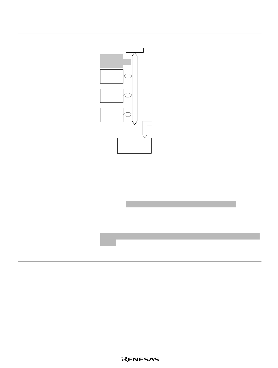
List of Items Revised or Added for This Version
Section Page Description
1.2 Block Diagram
Figure 1.1 Block
Diagram
2.5.1 Processor States
5.4 Memory-Mapped
Cache
5.4.1 Address Array
6
53
113
ASERAM deleted from figure
UDI
INTC
CPG/WDT
ASERAM deleted from legend
Description amended
In the power-on reset state, the internal states of the CPU and the
on-chip supporting module registers are initialized. In the manual
reset state, the internal states of the CPU and registers of on-chip
supporting modules other than the bus state controller (BSC) are
initialized.
the register configurations in the relevant sections for further
details.
Description amended
This operation is used to invalidate the address specification for a
cache. Write back will take place when the U bit of the entry that
received a hit is 1. Note that, when a 0 is written to the V bit, a 0
should always be written to the U bit of the same entry, too.
BRIDGE
I bus 2
External bus
interface
Refer to
Rev. 5.0, 09/03, page ix of xliv
Page 10

Section Page Description
5.4.3 Examples of
Usage
115,
116
(1) Invalidating a Specific Entry
Description amended
A specific cache entry can be invalidated by accessing the allocated
memory cache and writing a 0 to the entry’s U and V bits. The A bit is
cleared to 0, and an address is specified for the entry address and the
way. If the U bit of the way of the entry in question was set to 1, the
entry is written back and the V and U bits specified by the write data are
written to.
In the following example, the write data is specified in R0 and the
address is specified in R1.
; R0 = H'0000 0000 LRU = H'000, U = 0, V = 0
; R1 = H'F000
;
MOV.L R0, @R1
To invalidate all entries and ways, write 0 to the following addresses.
Addresses
This involves a total of 1, 024 writes.
The above operation should be performed using a non-cacheable area.
(2) Invalidating a Specific Address
Newly added
(3) Reading Data from a Specific Entry
Description amended
; R0 = H'F100 004C; Data array access, Entry = H'04,
; Way = 0, Longword address = 3
;
MOV.L R0, @R1 ; Longword 3 is read.
6.2.6 Interrupt
Exception Handling and
Priority
127
IPR (bit numbers) for SCI amended
(Before)IPRB(3-0) → (After)IPRB
Table 6.4 Interrupt
Exception Handling
Sources and Priority
(IRQ Mode)
6.3.6 Interrupt
Request Register 0
(IRR0)
138
Description amended
When clearing an IRQ5R–IRQ0R bit to 0, read the bit while bit set
to 1, and then write 0. In this case, 0 should be written only to the
bits to be cleared and 1 to the other bits. The co nten ts of the bits
to which 1 is written do not change.
8.2.1 Standby Control
Register (STBCR)
184
Description added
Bit 1—Module Standby 1 (MSTP1)
Before switching the RTC to module standby, access at least one
among the registers RTC, SCI, and TMU.
Rev. 5.0, 09/03, page x of xliv
1080, Way = 1, Entry = H'08, A = 0
F000 0000
F000 0010
F000 0020
:
F000 3FF0
(7-4)
Page 11

Section Page Description
8.3.3 Precautions
187
Newley added
when Using the Sleep
Mode
8.5.1 Transition to
Module Standby
Function
191
Note *3 added to bit table
3. Before putting the RTC into module standby status, first
Note:
access one or more of the RTC, SCI, and TMU
registers. The RTC may then be put into module standby
status.
9.3 Clock Operating
Modes
Table 9.4 Available
Combinations of Clock
210
2. under cautions amended
The peripheral clock frequency should not be set higher than the
frequency of the CKIO pin, higher than
Mode and FRQCR
Values
9.5.1 Changing the
Multiplication Rate
213
Description added
5.Supply of the clock that has been set begins at WDT count
overflow, and the processor begins operating again. The WDT
stops after it overflows.
When the following three conditions are all met, FRQCR should
not be changed while a DMAC transfer is in progress.
• Bits IFC2 to IFC0 are changed.
• STC2 to STC0 are not changed.
• The clock ratio of Iφ (on-chip clock) to Bφ (bus clock) after the
change is other than 1:1.
9.8.2 Changing the
Frequency
218,
219
Description added
5.The counter stops at a value of H'00 or H'01. The stop value
depends on the clock ratio.
When the following three conditions are all met, FRQCR should
not be changed while a DMAC transfer is in progress.
• Bits IFC2 to IFC0 are changed.
• STC2 to STC0 are not changed.
• The clock ratio of Iφ (on-chip clock) to Bφ (bus clock) after the
change is other than 1:1.
10.1.1 Features
10.2.5 Individual
Memory Control
Register (MCR)
223
246
Refresh function description deleted
Description added
Bit 7—Synchronous DRAM Bank Active (RASD): Specifies
whether synchronous DRAM is used in bank active mode or autoprecharge mode. Set auto-precharge mode when areas 2 and 3
are both designated as synchronous DRAM space.
The bank active mode should not be used unless the bus width
for all areas is 32 bits.
33.34 MHz.
Rev. 5.0, 09/03, page xi of xliv
Page 12
Section Page Description
A
10.2.13 MCS0 Control
Register (MCSCR0)
258
Description added
Bit 6—CS2/CS0 Select (CS2/0)
Only 0 should be used for the CS2/0 bit in MCSCR0. Either 0 or 1
may be used for MCSCR1 to MCSCR7.
10.3.4 Synchronous
DRAM Interface
290
Bank Active description added
… .In bank active mode, too, all banks become inactive after a
refresh cycle or after the bus is released as the result of bus
arbitration.
The bank active mode should not be used unless the bus width
for all areas is 32 bits.
10.3.6 PCMCIA
Interface
Figure 10.32 Basic
Timing for PCMCIA
310
Figure amended
D15 to D0
Write)
(
Memory Card Interface
10.3.7 Waits between
320
Figure amended
Access Cycles
Figure 10.40 Waits
between Access Cycles
CKIO
25 to A0
T
1
T2Twait T
T2Twait T
1
T
1
2
10.3.10 MCS[0] to
MCS[7] Pin Control
11.6 Usage Notes
13.4.3 Precautions
when Using RTC
Module Standby
323
387
426
Description amended
This enables 32-, 64-, 128-, or 256-Mbit memory to be connected
to area 0 or area 2.
However, only CS2/0 = 0 (area 0) should be
used for MCSCR0. Table 10.15 shows MCSCR0 – MCSCR7
settings and MCS[0]–MCS[7] assertion conditions.
Description added
13. DMAC transfers should not be perfor me d in the sleep mode
under conditions other than when the clock ratio of Iφ (on-
chip clock) to Bφ (bus clock) is 1:1.
14. When the following three conditions are all met, the
frequency control register (FRQCR) should not be changed
while a DMAC transfer is in progress.
• Bits IFC2 to IFC0 are changed.
• STC2 to STC0 in FRQCR are not changed.
• The clock ratio of Iφ (on-chip clock) to Bφ (bus clock) after
the change is other than 1:1.
Newly added
Rev. 5.0, 09/03, page xii of xliv
Page 13

Section Page Description
16.4 SCIF Interrupts
550
Description amended
When the TDFE flag in the serial status register (SCSSR) is set to
1, a TXI interrupt request is generated. The DMAC can be
activated and data transfer performed when this interrupt is
generated.
written to the transmit data register (SCFTDR) by the DMAC, 1 is
read from the TDFE flag, after which 0 is written to it to clear it.
When the RDF flag in SCSSR is set to 1, an RXI interrupt request
is generated. The DMAC can be activated and data transfer
performed when the RDF flag in SCSSR is set to 1. When
receive data less than the receive trigger number is read from the
receive data register (SCFRDR) by the DMAC, 1 is read from the
RDF flag, after which 0 is written to it to clear it.
16.5 Usage Notes
551
Description amended
1. SCFTDR Writing and TDFE Flag:
However, if the number of data bytes written to SCFTDR is equal
to or less than the transmit trigger number,
set to 1 again even after having been cleared to 0. TDFE clearing
should therefore be carried out after data exceeding the specified
transmit trigger number has been written to SCFTDR.
2. SCFRDR Reading and RDF Flag:
However, if the number of data bytes in SCFRDR exceeds the
trigger number, the RDF flag will be set to 1 again even after
having been cleared to 0. RDF should therefore be cleared to 0
after being read as 1 after all the receive data has been read.
19.13.2 SC Port Data
610
Title Amended
Register (SCPDR)
When data exceeding the transmit trigger number is
the TDFE flag will be
Rev. 5.0, 09/03, page xiii of xliv
Page 14
Section Page Description
20.3 Bus Master
Interface
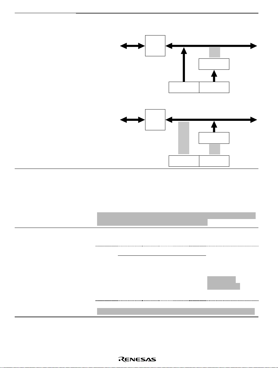
Figure 20.2 A/D Data
Register Access
Operation (Reading
H'AA40)
622
Figure amended
Upper byte read
CPU
receives
data H'AA
Bus
interface
Module internal data bus
TEMP
[H'40]
23.1 Absolute
Maximum Ratings
Table 23.1 Absolute
Maximum Ratings
23.2 DC
Characteristics
Table 23.2 DC
Characteristics
657
659,
662
ADDRn L
[H'40]
Module internal data bus
TEMP
[H'40]
ADDRn L
[H'40]
n = A to D
n = A to D
Lower byte read
CPU
receives
data H'40
Bus
interface
ADDRn H
[H'AA]
ADDRn H
[H'AA]
Caution added
2.Until voltage is applied to all power supplies, a low level is input
at the RESETP pin, and CKIO has operated for a maximum of 4
clock cycles, internal circuits remain unsettled, and so pin states
are also undefin ed. The system design must ensure that these
undefined states do not cause erroneous system operation.
Note that the RESETP pin cannot receive a low level signal while
a low level signal is being input to the CA pin.
Test conditions for in sleep mode amended
Item Symbol Min Typ Max Unit Test Conditions
Sleep
mode
Icc — 15 30
1
*
IccQ — 10 20
1
: When there is no
*
other external bus
cycle other than the
refresh cycle.
Vcc = 1.9 V
VccQ = 3.3 V
Bφ = 33MHz
Note * added
* If the IRL and IRLS interrupts are used, the minimum is 1.9 V.
Rev. 5.0, 09/03, page xiv of xliv
Page 15
Section Page Description
A
A
A
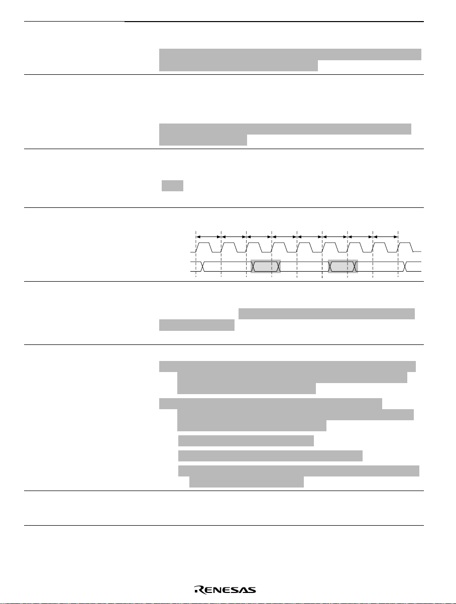
23.3.6 Synchronous
DRAM Timing
690
Tnop cycle deleted from figure
Tc1 Tc2 Tc3/Td1 Tc4/Td2 Td3 Td4
Figure 23.31
Synchronous DRAM
Burst Read Bus Cycle
(RAS Down, Same Row
Address, CAS Latency
= 2)
CKIO
25 to A16
12 or A10
15 to A0
CSn
RD/WR
RAS
CAS
DQMxx
D31 to D0
BS
t
AD
t
AD
t
AD
t
CSD3
t
RWD
t
RASD2
t
CASD2
t
DQMD
Row address
Read command
Column address
t
RDS2
t
BSD
t
RDH2
t
AD
t
AD
t
CASD2
t
RDS2
t
AD
t
CSD3
t
RWD
t
DQMD
t
RDH2
t
BSD
CKE
DACKn
(High)
t
DAKD1
t
DAKD1
Rev. 5.0, 09/03, page xv of xliv
Page 16
Section Page Description
A.2 Pin Specifications
Table A.2 Pin
Specifications
723
Function information amend ed for VCC–RTC, VCC–PLL1, VCC–
PLL2, and V
Pin Pin No.
(FP-208C,
FP-208E)
V
–
3 E2 Power
CC
RTC
145
VCC–
150
PLL1
–
V
CC
PLL2
V
29, 81,
CC
134, 154,
175
CC
Pin No.
(BP-
240A)
F16,
E17
L3, L4,
U11, T11,
J17, J16,
E18, C19,
C12, D12
I/O Function
RTC oscillator power
supply
supply
(2.0/1.9/1.8/1.7 V)
Power
supply
Power
supply
PLL power supply
(2.0/1.9/1.8/1.7 V)
Internal power supply
(2.0/1.9/1.8/1.7 V)
A.3 Treatment of
Unused Pins
A.4 Pin States in
Access to Each
Address Space
Table A.3 Pin States
(Ordinary Memory/Little
Endian)
Table A.4 Pin States
(Ordinary Memory/Big
Endian)
Table A.5 Pin States
(Burst ROM/Little
Endian)
Table A.6 Pin States
(Burst ROM/Big
Endian)
Table A.9 Pin States
(PCMCIA/Little Endian)
Table A.10 Pin States
(PCMCIA/Big Endian)
724
726 to
738
"When RTC is not used" and "When PLL2 is not used" amended
(Before) (1.9/1.8V) →(After) (
2.0/1.9/1.8/1.7V)
Note 2 amended
Note: 2.Unused data pins should be switched to the port
function, or
pulled up.
Rev. 5.0, 09/03, page xvi of xliv
Page 17

Contents
Section 1 Overview and Pin Functions
1.1 SH7709S Features .............................................................................................................1
1.2 Block Diagram .................................................................................................................. 6
1.3 Pin Description.................................................................................................................. 7
1.3.1 Pin Assignment .................................................................................................... 7
1.3.2 Pin Function ......................................................................................................... 9
Section 2 CPU
2.1 Register Configuration ...................................................................................................... 19
2.1.1 Privileged Mode and Banks.................................................................................. 19
2.1.2 General Registers ................................................................................................. 22
2.1.3 System Registers.................................................................................................. 23
2.1.4 Control Registers.................................................................................................. 23
2.2 Data Formats ..................................................................................................................... 25
2.2.1 Data Format in Registers...................................................................................... 25
2.2.2 Data Format in Memory....................................................................................... 25
2.3 Instruction Features ........................................................................................................... 26
2.3.1 Execution Environment........................................................................................ 26
2.3.2 Addressing Modes................................................................................................ 28
2.3.3 Instruction Formats............................................................................................... 32
2.4 Instruction Set.................................................................................................................... 35
2.4.1 Instruction Set Classified by Function.................................................................. 35
2.4.2 Instruction Code Map........................................................................................... 50
2.5 P rocessor States and Processor Modes.............................................................................. 53
2.5.1 Processor States.................................................................................................... 53
2.5.2 Processor Modes .................................................................................................. 54
....................................................................................................................... 19
.......................................................................... 1
Section 3 Memory Management Unit (MMU)
3.1 Overview ........................................................................................................................... 55
3.1.1 Features................................................................................................................ 55
3.1.2 Role of MMU....................................................................................................... 55
3.1.3 SH7709S MMU.................................................................................................... 58
3.1.4 Register Configuration......................................................................................... 61
3.2 Register Description.......................................................................................................... 61
3.3 TLB Functions................................................................................................................... 63
3.3.1 Configuration of the TLB..................................................................................... 63
3.3.2 TLB Indexing....................................................................................................... 65
3.3.3 TLB Address Comparison.................................................................................... 66
3.3.4 Page Management Information............................................................................ 68
............................................................ 55
Rev. 5.00, 09/03, page xvii of xliv
Page 18

3.4 MMU Functions................................................................................................................69
3.4.1 MMU Hardware Management ............................................................................. 69
3.4.2 MMU Software Management............................................................................... 69
3.4.3 MMU Instruction (LDTLB)................................................................................. 70
3.4.4 Avoiding Synonym Problems............................................................................... 72
3.5 MMU Exceptions .............................................................................................................. 74
3.5.1 TLB Miss Exception ............................................................................................ 74
3.5.2 TLB Protection Violation Exception.................................................................... 75
3.5.3 TLB Invalid Exception......................................................................................... 76
3.5.4 Initial Page Write Exception ................................................................................ 77
3.5.5 Processing Flow in Event of MMU Exception (Same Processing Flow
for Address Error)................................................................................................ 79
3.6 Configuration of Memory-Mapped TLB........................................................................... 80
3.6.1 Address Array ...................................................................................................... 80
3.6.2 Data Array............................................................................................................ 81
3.6.3 Usage Examples................................................................................................... 83
3.7 Usage Note ........................................................................................................................ 83
Section 4 Exception Handling
4.1 Overview ........................................................................................................................... 85
4.1.1 Features................................................................................................................ 85
4.1.2 Register Configuration......................................................................................... 85
4.2 Exception Handling Function............................................................................................ 85
4.2.1 Exception Handling Flow..................................................................................... 85
4.2.2 Exception Vector Addresses................................................................................. 86
4.2.3 Acceptance of Exceptions.................................................................................... 88
4.2.4 Exception Codes................................................................................................... 90
4.2.5 Exception Request Masks .................................................................................... 91
4.2.6 Returning from Exception Handling .................................................................... 91
4.3 Register Descriptions......................................................................................................... 92
4.4 Exception Handling Operation .......................................................................................... 93
4.4.1 Reset..................................................................................................................... 93
4.4.2 Interrupts.............................................................................................................. 93
4.4.3 General Exceptions............................................................................................... 94
4.5 Individual Exception Operations....................................................................................... 94
4.5.1 Resets ................................................................................................................... 94
4.5.2 General Exceptions............................................................................................... 95
4.5.3 Interrupts.............................................................................................................. 99
4.6 Cautions............................................................................................................................. 100
Section 5 Cache
5.1 Overview ........................................................................................................................... 103
5.1.1 Features................................................................................................................ 103
.................................................................................................................... 103
.......................................................................................... 85
Rev. 5.00, 09/03, page xviii of xliv
Page 19

5.1.2 Cache Structure.................................................................................................... 103
5.1.3 Register Configuration......................................................................................... 105
5.2 Register Description.......................................................................................................... 105
5.2.1 Cache Control Register (CCR)............................................................................. 105
5.2.2 Cache Control Register 2 (CCR2)........................................................................ 106
5.3 Cache Operation................................................................................................................ 109
5.3.1 Searching the Cache............................................................................................. 109
5.3.2 Read Access......................................................................................................... 111
5.3.3 Prefetch Operation................................................................................................ 111
5.3.4 Write Access ........................................................................................................ 111
5.3.5 Write-Back Buffer................................................................................................ 111
5.3.6 Coherency of Cache and External Memory.......................................................... 112
5.4 Me mory-Mapped Cache.................................................................................................... 112
5.4.1 Address Array ...................................................................................................... 112
5.4.2 Data Array............................................................................................................ 113
5.4.3 Examples of Usage............................................................................................... 115
Section 6 Interrupt Controller (INTC)
6.1 Overview ........................................................................................................................... 117
6.1.1 Features................................................................................................................ 117
6.1.2 Block Diagram ..................................................................................................... 118
6.1.3 Pin Configuration................................................................................................. 119
6.1.4 Register Configuration......................................................................................... 120
6.2 Interrupt Sources ............................................................................................................... 121
6.2.1 NMI Interrupt....................................................................................................... 121
6.2.2 IRQ Interrupts ...................................................................................................... 121
6.2.3 IRL Interrupts....................................................................................................... 122
6.2.4 PINT Interrupts .................................................................................................... 124
6.2.5 On-Chip Peripheral Module Interrupts................................................................. 124
6.2.6 Interrupt Exception Handling and Priority........................................................... 125
6.3 INTC Registers.................................................................................................................. 131
6.3.1 Interrupt Priority Registers A to E (IPRA–IPRE) ................................................ 131
6.3.2 Interrupt Control Register 0 (ICR0)..................................................................... 132
6.3.3 Interrupt Control Register 1 (ICR1)..................................................................... 133
6.3.4 Interrupt Control Register 2 (ICR2)..................................................................... 136
6.3.5 PINT Interrupt Enable Register (PINTER).......................................................... 137
6.3.6 Interrupt Request Register 0 (IRR0)..................................................................... 138
6.3.7 Interrupt Request Register 1 (IRR1)..................................................................... 140
6.3.8 Interrupt Request Register 2 (IRR2)..................................................................... 141
6.4 INTC Operation................................................................................................................. 143
6.4.1 Interrupt Sequence................................................................................................ 143
6.4.2 Multiple Interrupts................................................................................................ 145
6.5 Interrupt Response Time ................................................................................................... 145
........................................................................... 117
Rev. 5.00, 09/03, page xix of xliv
Page 20

Section 7 User Break Controller
7.1 Overview ........................................................................................................................... 149
7.1.1 Features................................................................................................................ 149
7.1.2 Block Diagram ..................................................................................................... 150
7.1.3 Register Configuration......................................................................................... 151
7.2 Register Descriptions......................................................................................................... 152
7.2.1 Break Address Register A (BARA )...................................................................... 152
7.2.2 Break Address Mask Register A (BAMRA)........................................................ 153
7.2.3 Break Bus Cycle Register A (BBRA).................................................................. 154
7.2.4 Break Address Register B (BARB)...................................................................... 156
7.2.5 Break Address Mask Register B (BAMRB)......................................................... 157
7.2.6 Break Data Register B (BDRB) ........................................................................... 158
7.2.7 Break Data Mask Register B (BDMRB).............................................................. 159
7.2.8 Break Bus Cycle Register B (BBRB)................................................................... 160
7.2.9 Break Control Register (BRCR)........................................................................... 162
7.2.10 Execution Times Break Register (BETR)............................................................ 166
7.2.11 Branch Source Register (BRSR) .......................................................................... 167
7.2.12 Branch Destination Register (BRDR) .................................................................. 168
7.2.13 Break A S ID Register A (BASRA )....................................................................... 169
7.2.14 Break A S ID Register B (BASR B) ....................................................................... 169
7.3 Operation Description ....................................................................................................... 170
7.3.1 Flow of the User Break Operation........................................................................ 170
7.3.2 Break on Instruction Fetch Cycle......................................................................... 170
7.3.3 Break by Data Access Cycle ................................................................................ 171
7.3.4 Sequential Break .................................................................................................. 172
7.3.5 Value of Saved Program Counter......................................................................... 172
7.3.6 PC Trace............................................................................................................... 173
7.3.7 Usage Examples................................................................................................... 174
7.3.8 Notes .................................................................................................................... 179
...................................................................................... 149
Section 8 Power-Down Modes
8.1 Overview ........................................................................................................................... 181
8.1.1 Power-Down Modes............................................................................................. 181
8.1.2 Pin Configuration................................................................................................. 183
8.1.3 Register Configuration......................................................................................... 183
8.2 Register Descriptions......................................................................................................... 183
8.2.1 Standby Control Register (STBCR)..................................................................... 183
8.2.2 Standby Control Register 2 (STBCR2)................................................................ 185
8.3 Sleep Mode........................................................................................................................ 187
8.3.1 Transition to Sleep Mode..................................................................................... 187
8.3.2 Canceling Sleep Mode.......................................................................................... 187
8.3.3 Precautions when Using the Sleep Mode............................................................. 187
8.4 Standb y Mode.................................................................................................................... 188
Rev. 5.00, 09/03, page xx of xliv
......................................................................................... 181
Page 21

8.4.1 Transition to Standby Mode................................................................................. 188
8.4.2 Canceling Standby Mode ..................................................................................... 189
8.4.3 Clock Pause Function........................................................................................... 190
8.5 Module Standby Function ................................................................................................. 191
8.5.1 Transition to Module Standby Function............................................................... 191
8.5.2 Clearing Module Standby Function...................................................................... 191
8.6 Timing of STATUS Pin Changes...................................................................................... 192
8.6.1 Timing for Resets ................................................................................................. 192
8.6.2 Timing for Canceling Standby ............................................................................. 194
8.6.3 Timing for Canceling Sleep Mode....................................................................... 196
8.7 Hardware Standby Mode................................................................................................... 199
8.7.1 Transition to Hardware Standby Mode ................................................................ 199
8.7.2 Canceling Hardware Standby Mode..................................................................... 199
8.7.3 Hardware Standby Mode Timing......................................................................... 200
Section 9 On-Chip Oscillation Circuits
9.1 Overview ........................................................................................................................... 203
9.1.1 Features................................................................................................................ 203
9.2 Overview of CPG .............................................................................................................. 204
9.2.1 CPG Block Diagram............................................................................................. 204
9.2.2 CPG Pin Configuration ........................................................................................ 206
9.2.3 CPG Register Configuration................................................................................. 206
9.3 Clock Operating Modes..................................................................................................... 207
9.4 Register Descriptions......................................................................................................... 211
9.4.1 Frequency Control Register (FRQCR)................................................................. 211
9.5 Changing the Frequency.................................................................................................... 213
9.5.1 Changing the Multiplication Rate ........................................................................ 213
9.5.2 Changing the Division Ratio................................................................................ 213
9.6 Overview of WDT............................................................................................................. 214
9.6.1 Block Diagram of WDT....................................................................................... 214
9.6.2 Register Configuration......................................................................................... 214
9.7 W DT Registers.................................................................................................................. 215
9.7.1 Watchdog Timer Counter (WTCNT)................................................................... 215
9.7.2 Watchdog Timer Control/Status Register (WTCSR) ........................................... 215
9.7.3 Notes on Register Access..................................................................................... 217
9.8 Using the WDT ................................................................................................................. 218
9.8.1 Canceling Standby................................................................................................ 218
9.8.2 Changing the Frequency....................................................................................... 218
9.8.3 Using Watchdog Timer Mode.............................................................................. 219
9.8.4 Using Interval Timer Mode.................................................................................. 219
9.9 Notes on Board Design...................................................................................................... 220
......................................................................... 203
Rev. 5.00, 09/03, page xxi of xliv
Page 22

Section 10 Bus State Controller (BSC)
10.1 Overview ........................................................................................................................... 223
10.1.1 Features................................................................................................................ 223
10.1.2 Block Diagram..................................................................................................... 225
10.1.3 Pin Conf iguration................................................................................................. 226
10.1.4 Register Configuration......................................................................................... 228
10.1.5 Area Overview ..................................................................................................... 229
10.1.6 PCMCIA Support................................................................................................. 232
10.2 BSC Registers.................................................................................................................... 235
10.2.1 Bus Control Register 1 (BCR1)............................................................................ 235
10.2.2 Bus Control Register 2 (BCR2)............................................................................ 239
10.2.3 Wait State Control Register 1 (WCR1)................................................................ 240
10.2.4 Wait State Control Register 2 (WCR2)................................................................ 241
10.2.5 Individual Memory Control Register (MCR)....................................................... 245
10.2.6 PCMCIA Control Register (PCR)........................................................................ 248
10.2.7 Synchronous DRAM Mode Register (SDMR)..................................................... 252
10.2.8 Refresh Timer Control/Status Register (RTCSR) ................................................ 253
10.2.9 Refresh Timer Counter (RTCNT)........................................................................ 255
10.2.10 Refresh Time Constant Register (RTCOR).......................................................... 256
10.2.11 Refresh Count Register (RFCR)........................................................................... 256
10.2.12 Cautions on Accessing Refresh Control Related Registers.................................. 257
10.2.13 MCS0 Control Register (MCSCR0)..................................................................... 258
10.2.14 MCS1 Control Register (MCSCR1)..................................................................... 259
10.2.15 MCS2 Control Register (MCSCR2)..................................................................... 259
10.2.16 MCS3 Control Register (MCSCR3)..................................................................... 259
10.2.17 MCS4 Control Register (MCSCR4)..................................................................... 259
10.2.18 MCS5 Control Register (MCSCR5)..................................................................... 259
10.2.19 MCS6 Control Register (MCSCR6)..................................................................... 259
10.2.20 MCS7 Control Register (MCSCR7)..................................................................... 259
10.3 BSC Operation .................................................................................................................. 260
10.3.1 Endian/Access Size and Data Alignment............................................................. 260
10.3.2 Description of Areas............................................................................................. 265
10.3.3 Basic Interface...................................................................................................... 268
10.3.4 Synchronous DRAM Interface............................................................................. 276
10.3.5 Burst ROM Interface............................................................................................ 304
10.3.6 PCMCIA Interface ............................................................................................... 307
10.3.7 Waits betw een Access Cycles.............................................................................. 319
10.3.8 Bus Arbitration..................................................................................................... 320
10.3.9 Bus Pull-U p.......................................................................................................... 321
10.3.10 MCS[0] to MCS[7] Pin Control........................................................................... 323
......................................................................... 223
Section 11 Direct Memory Access Controller (DMAC)
11.1 Overview ........................................................................................................................... 327
Rev. 5.00, 09/03, page xxii of xliv
.......................................... 327
Page 23

11.1.1 Features................................................................................................................ 327
11.1.2 Block Diagram..................................................................................................... 329
11.1.3 Pin Conf iguration................................................................................................. 330
11.1.4 Register Configuration......................................................................................... 331
11.2 Register Descriptions......................................................................................................... 333
11.2.1 DMA Source Address Registers 0–3 (SAR0–SAR3)........................................... 333
11.2.2 DMA Destinat i on Address Registers 0–3 (DAR0–DAR3).................................. 334
11.2.3 DMA Transfer Count Registers 0–3 (DMATCR0–DMATCR3)......................... 335
11.2.4 DMA Channel Control Registers 0–3 (CHCR0–CHCR3) ................................... 336
11.2.5 DMA Operation Register (DMAOR)................................................................... 343
11.3 Operation........................................................................................................................... 345
11.3.1 DMA Transfer Flow............................................................................................. 345
11.3.2 DMA Transfer Requests....................................................................................... 347
11.3.3 Channel Priority................................................................................................... 349
11.3.4 DMA Transfer Types ........................................................................................... 352
11.3.5 Number of Bus Cycle States and DREQ Pin Sampling Timing........................... 363
11.3.6 Source Address Reload Function......................................................................... 372
11.3.7 DMA Transfer Ending Conditions....................................................................... 374
11.4 Compare Match Timer (CMT).......................................................................................... 376
11.4.1 Overview.............................................................................................................. 376
11.4.2 Register Descriptions ........................................................................................... 377
11.4.3 Operation.............................................................................................................. 380
11.4.4 Compare Match.................................................................................................... 381
11.5 Examples of Use................................................................................................................ 383
11.5.1 Example of DMA Transfer between On-Chip IrDA and External Memory ........ 383
11.5.2 Example of DMA Transfer between A/D Converter and External Memory........ 384
11.5.3 Example of DMA Transfer between External Memory and SCIF Transmitter
(Indirect Address On)........................................................................................... 385
11.6 Usage Notes....................................................................................................................... 387
Section 12 Timer (TMU)
12.1 Overview ........................................................................................................................... 389
12.1.1 Features................................................................................................................ 389
12.1.2 Block Diagram..................................................................................................... 390
12.1.3 Pin Conf iguration................................................................................................. 391
12.1.4 Register Configuration......................................................................................... 391
12.2 TMU Registers .................................................................................................................. 392
12.2.1 Timer Output Control Register (TOCR) .............................................................. 392
12.2.2 Timer Start Register (TSTR)................................................................................ 392
12.2.3 Timer Control Registers (TCR)............................................................................ 393
12.2.4 Timer Constant Registers (TCOR) ....................................................................... 397
12.2.5 Timer Counters (TCNT)....................................................................................... 397
12.2.6 Input Capture Register (TCPR2).......................................................................... 399
................................................................................................... 389
Rev. 5.00, 09/03, page xxiii of xliv
Page 24

12.3 TMU Operation................................................................................................................. 400
12.3.1 General Operation................................................................................................ 400
12.3.2 Input Capture Function......................................................................................... 403
12.4 Interrupts ........................................................................................................................... 404
12.4.1 Status Flag Setting Timing................................................................................... 404
12.4.2 Status Flag C learing Timing................................................................................. 405
12.4.3 Interrupt Sources and Priorities............................................................................ 405
12.5 Usage Notes....................................................................................................................... 406
12.5.1 Writing to Registers.............................................................................................. 406
12.5.2 Reading Registers................................................................................................. 406
Section 13 Realtime Clock (RTC)
13.1 Overview ........................................................................................................................... 407
13.1.1 Features................................................................................................................ 407
13.1.2 Block Diagram..................................................................................................... 408
13.1.3 Pin Conf iguration................................................................................................. 409
13.1.4 RTC Register Configuration................................................................................. 410
13.2 RTC Registers ................................................................................................................... 411
13.2.1 64-Hz Counter (R64CNT).................................................................................... 411
13.2.2 Second Counter (RSECCNT)............................................................................... 411
13.2.3 Minute Counter (RMINCNT) .............................................................................. 412
13.2.4 Hour Counter (RHRCNT).................................................................................... 412
13.2.5 Day of Week Counter (RWKCNT)...................................................................... 413
13.2.6 Date Counter (RDAYCNT).................................................................................. 414
13.2.7 Month Counter (RMONCNT).............................................................................. 414
13.2.8 Year Counter (RYRCNT) .................................................................................... 415
13.2.9 Second Alarm Register (RSECAR)...................................................................... 415
13.2.10 Minute Alarm Register (RMINAR) ..................................................................... 416
13.2.11 Hour Alarm Register (RHRAR)........................................................................... 416
13.2.12 Day of Week Alarm Register (RWKAR)............................................................. 417
13.2.13 Date Alarm Register (RDAYAR) ........................................................................ 418
13.2.14 Month Alarm Register (RMONAR)..................................................................... 418
13.2.15 RTC Control Register 1 (RCR1).......................................................................... 419
13.2.16 RTC Control Register 2 (RCR2) .......................................................................... 420
13.3 RTC Operation .................................................................................................................. 422
13.3.1 Initial Settings of Registers after Power-On......................................................... 422
13.3.2 Setting the Time................................................................................................... 422
13.3.3 Reading the Time ................................................................................................. 423
13.3.4 Alarm Fun ction .................................................................................................... 424
13.3.5 Crystal Oscillator Circuit...................................................................................... 425
13.4 Usage Notes....................................................................................................................... 426
13.4.1 Register Writing during RTC Count .................................................................... 426
13.4.2 Use of Realtime Clock (RTC) Periodic Interrupts ............................................... 426
.................................................................................. 407
Rev. 5.00, 09/03, page xxiv of xliv
Page 25

13.4.3 Precautions when Using RTC Module Standby................................................... 426
Section 14 Serial Communication Interface (SCI)
14.1 Overview ........................................................................................................................... 427
14.1.1 Features................................................................................................................ 427
14.1.2 Block Diagram..................................................................................................... 428
14.1.3 Pin Conf iguration................................................................................................. 431
14.1.4 Register Configuration......................................................................................... 432
14.2 Register Descriptions......................................................................................................... 432
14.2.1 Receive Shift Register (SCRSR).......................................................................... 432
14.2.2 Receive Data Register (SCRDR).......................................................................... 433
14.2.3 Transmit Shift Register (SCTSR)......................................................................... 433
14.2.4 Transmit Data Register (SCTDR) ........................................................................ 434
14.2.5 Serial Mode Register (SCSMR)........................................................................... 434
14.2.6 Serial Control Register (SCSCR)......................................................................... 437
14.2.7 Serial Status R egister (S CSSR)............................................................................ 440
14.2.8 SC Port Control Register (SCPCR)/SC Port Data Register (SCPDR)................. 444
14.2.9 Bit Rate Register (SCBRR).................................................................................. 446
14.3 Operation........................................................................................................................... 453
14.3.1 Overview.............................................................................................................. 453
14.3.2 Operation in Asynch ronous Mode........................................................................ 455
14.3.3 Multiprocessor Communication........................................................................... 465
14.3.4 Synchronous Operation........................................................................................ 474
14.4 SCI Interrupts.................................................................................................................... 484
14.5 Usage Notes....................................................................................................................... 485
..................................................... 427
Section 15 Smart Card Interface
15.1 Overview ........................................................................................................................... 489
15.1.1 Features................................................................................................................ 489
15.1.2 Block Diagram..................................................................................................... 490
15.1.3 Pin Conf iguration................................................................................................. 491
15.1.4 Smart Card Interface Registers............................................................................. 491
15.2 Register Descriptions......................................................................................................... 492
15.2.1 Smart Card Mode Register (SCSCMR)................................................................ 492
15.2.2 Serial Status R egister (S CSSR)............................................................................ 493
15.3 Operation........................................................................................................................... 494
15.3.1 Overview.............................................................................................................. 494
15.3.2 Pin Conn ections.................................................................................................... 495
15.3.3 Data Format.......................................................................................................... 496
15.3.4 Register Settings................................................................................................... 497
15.3.5 Clock.................................................................................................................... 498
15.3.6 Data Transmission and Reception........................................................................ 501
15.4 Usage Notes....................................................................................................................... 507
...................................................................................... 489
Rev. 5.00, 09/03, page xxv of xliv
Page 26

15.4.1 Receive Data Timing and Receive Margin in Asynchronous Mode .................... 507
15.4.2 Retransmission (Receive and Transmit Modes)................................................... 509
Section 16 Serial Communication Interface with FIFO (SCIF)
16.1 Overview ........................................................................................................................... 511
16.1.1 Features................................................................................................................ 511
16.1.2 Block Diagram..................................................................................................... 512
16.1.3 Pin Conf iguration................................................................................................. 515
16.1.4 Register Configuration......................................................................................... 516
16.2 Register Descriptions......................................................................................................... 517
16.2.1 Receive Shift Register (SCRSR).......................................................................... 517
16.2.2 Receive FIFO Data Register (SCFRDR).............................................................. 517
16.2.3 Transmit Shift Register (SCTSR)......................................................................... 517
16.2.4 Transmit FIFO Data Register (SCFTDR) ............................................................ 518
16.2.5 Serial Mode Register (SCSMR)........................................................................... 518
16.2.6 Serial Control Register (SCSCR)......................................................................... 520
16.2.7 Serial Status R egister (S CSSR)............................................................................ 522
16.2.8 Bit Rate Register (SCBRR).................................................................................. 527
16.2.9 FIFO Control Register (SCFCR).......................................................................... 534
16.2.10 FIFO Data Count Register (SCFDR) ................................................................... 536
16.3 Operation........................................................................................................................... 537
16.3.1 Overview.............................................................................................................. 537
16.3.2 Serial Operation.................................................................................................... 538
16.4 SCIF Interrupts.................................................................................................................. 550
16.5 Usage Notes....................................................................................................................... 551
............................. 511
Section 17 IrDA
17.1 Overview ........................................................................................................................... 555
17.1.1 Features................................................................................................................ 555
17.1.2 Block Diagram..................................................................................................... 556
17.1.3 Pin Conf iguration................................................................................................. 559
17.1.4 Register Configuration......................................................................................... 560
17.2 Register Description.......................................................................................................... 561
17.2.1 Serial Mode Register (SCSMR)........................................................................... 561
17.3 Operation Description ....................................................................................................... 563
17.3.1 Overview.............................................................................................................. 563
17.3.2 Transmitting......................................................................................................... 563
17.3.3 Receiving.............................................................................................................. 564
Section 18 Pin Function Controller
18.1 Overview ........................................................................................................................... 565
18.2 Register Configuration ...................................................................................................... 569
18.3 Register Descriptions......................................................................................................... 570
Rev. 5.00, 09/03, page xxvi of xliv
.................................................................................................................... 555
................................................................................ 565
Page 27

18.3.1 Port A Control Register (PACR).......................................................................... 570
18.3.2 Port B Control Register (PBCR) .......................................................................... 571
18.3.3 Port C Control Register (PCCR) .......................................................................... 572
18.3.4 Port D Control Register (PDCR).......................................................................... 573
18.3.5 Port E Control Register (PECR)........................................................................... 574
18.3.6 Port F Control R egister (PFCR)........................................................................... 575
18.3.7 Port G Control Register (PGCR).......................................................................... 576
18.3.8 Port H Control Register (PHCR).......................................................................... 577
18.3.9 Port J Control Register (PJCR) ............................................................................ 579
18.3.10 Port K Control Register (PKCR).......................................................................... 580
18.3.11 Port L Control Register (PLCR)........................................................................... 581
18.3.12 SC Port Control Register (SCPCR)...................................................................... 582
Section 19 I/O Ports
19.1 Overview ........................................................................................................................... 587
19.2 Port A ................................................................................................................................ 587
19.2.1 Register Description............................................................................................. 587
19.2.2 Port A Data Register (PADR) .............................................................................. 588
19.3 Port B ................................................................................................................................ 589
19.3.1 Register Description............................................................................................. 589
19.3.2 Port B Data Register (PBDR)............................................................................... 590
19.4 Port C ................................................................................................................................ 591
19.4.1 Register Description............................................................................................. 591
19.4.2 Port C Data Register (PCDR)............................................................................... 592
19.5 Port D ................................................................................................................................ 593
19.5.1 Register Description............................................................................................. 593
19.5.2 Port D Data Register (PDDR).............................................................................. 594
19.6 Port E................................................................................................................................. 595
19.6.1 Register Description............................................................................................. 595
19.6.2 Port E Data Register (PEDR)............................................................................... 596
19.7 Port F................................................................................................................................. 597
19.7.1 Register Description............................................................................................. 597
19.7.2 Port F Data Register (PFDR)................................................................................ 598
19.8 Port G ................................................................................................................................ 599
19.8.1 Register Description............................................................................................. 599
19.8.2 Port G Data Register (PGDR).............................................................................. 600
19.9 Port H ................................................................................................................................ 601
19.9.1 Register Description............................................................................................. 601
19.9.2 Port H Data Register (PHDR).............................................................................. 602
19.10 Port J.................................................................................................................................. 603
19.10.1 Register Description............................................................................................. 603
19.10.2 Port J Data Register (PJDR)................................................................................. 604
19.11 Port K ................................................................................................................................ 605
............................................................................................................ 587
Rev. 5.00, 09/03, page xxvii of xliv
Page 28

19.11.1 Register Description............................................................................................. 605
19.11.2 Port K Data Register (PKDR).............................................................................. 606
19.12 Port L................................................................................................................................. 607
19.12.1 Register Description............................................................................................. 607
19.12.2 Port L Data Register (PLDR)............................................................................... 608
19.13 SC Port .............................................................................................................................. 609
19.13.1 Register Description............................................................................................. 609
19.13.2 SC Port Data Register (SCPDR) .......................................................................... 610
Section 20 A/D Converter
20.1 Overview ........................................................................................................................... 613
20.1.1 Features................................................................................................................ 613
20.1.2 Block Diagram..................................................................................................... 614
20.1.3 Input Pins.............................................................................................................. 615
20.1.4 Register Configuration......................................................................................... 616
20.2 Register Descriptions......................................................................................................... 617
20.2.1 A/D Data Registers A to D (ADDRA to ADDRD).............................................. 617
20.2.2 A/D Control/Status Register (ADCSR)................................................................ 618
20.2.3 A/D Control Register (ADCR)............................................................................. 621
20.3 Bus Master Interface.......................................................................................................... 622
20.4 Operation........................................................................................................................... 623
20.4.1 Single Mode (MULTI = 0)................................................................................... 623
20.4.2 Multi Mode (MULTI = 1, SCN = 0) .................................................................... 625
20.4.3 Scan Mode (MULTI = 1, SCN = 1) ..................................................................... 627
20.4.4 Input Sampling and A/D Conversion Time.......................................................... 629
20.4.5 External Trigger Input Timing ............................................................................. 630
20.5 Interrupts ........................................................................................................................... 631
20.6 Definitions of A/D Conversion Accuracy ......................................................................... 631
20.7 Usage Notes....................................................................................................................... 632
20.7.1 Setting Analog Input Voltage............................................................................... 632
20.7.2 Processin g of Analog Input Pins .......................................................................... 632
20.7.3 Access Size and Read Data .................................................................................. 633
................................................................................................. 613
Section 21 D/A Converter
21.1 Overview ........................................................................................................................... 635
21.1.1 Features................................................................................................................ 635
21.1.2 Block Diagram..................................................................................................... 635
21.1.3 I/O Pins................................................................................................................. 636
21.1.4 Register Configuration......................................................................................... 636
21.2 Register Descriptions......................................................................................................... 637
21.2.1 D/A Data Registers 0 and 1 (DADR0/1).............................................................. 637
21.2.2 D/A Control Register (DACR)............................................................................. 637
21.3 Operation........................................................................................................................... 639
Rev. 5.00, 09/03, page xxviii of xliv
................................................................................................. 635
Page 29

Section 22 User Debugging Interface (UDI)
22.1 Overview ........................................................................................................................... 641
22.2 User Debugging Interface (UDI)....................................................................................... 641
22.2.1 Pin Description s................................................................................................... 641
22.2.2 Block Diagram..................................................................................................... 642
22.3 Register Descriptions......................................................................................................... 642
22.3.1 Bypass Register (SDBPR).................................................................................... 643
22.3.2 Instruction Register (SDIR).................................................................................. 643
22.3.3 Boundary Scan Register (SDBSR)....................................................................... 644
22.4 UDI Operation................................................................................................................... 651
22.4.1 TAP Controller..................................................................................................... 651
22.4.2 Reset Configuration.............................................................................................. 652
22.4.3 UDI Reset............................................................................................................. 653
22.4.4 UDI Interrupt........................................................................................................ 653
22.4.5 Bypass.................................................................................................................. 653
22.4.6 Using UDI to Recover from Sleep Mode............................................................. 653
22.5 Boundary Scan .................................................................................................................. 654
22.5.1 Supported Instructions.......................................................................................... 654
22.5.2 Points for Attention.............................................................................................. 655
22.6 Usage Notes....................................................................................................................... 655
22.7 Advanced User Debugger (AUD) ..................................................................................... 655
............................................................... 641
Section 23 Electrical Characteristics
23.1 Absolute Maximum Ratings.............................................................................................. 657
23.2 DC Characteristics............................................................................................................. 659
23.3 AC Characteristics............................................................................................................. 663
23.3.1 Clock Tim ing........................................................................................................ 664
23.3.2 Control Sig nal Timing.......................................................................................... 670
23.3.3 AC Bu s Timing .................................................................................................... 673
23.3.4 Basic Timing........................................................................................................ 675
23.3.5 Burst ROM Timing .............................................................................................. 678
23.3.6 Synchronous DRAM Timing ............................................................................... 681
23.3.7 PCMCIA Timing .................................................................................................. 699
23.3.8 Peripheral Module Signal Timing........................................................................ 706
23.3.9 UDI-Related Pin Timing...................................................................................... 709
23.3.10 AC Characteristics Measurement Conditions....................................................... 711
23.3.11 Delay Time Variation Due to Load Capacitance.................................................. 712
23.4 A/D Converter Characteristics........................................................................................... 713
23.5 D/A Converter Characteristics........................................................................................... 713
Appendix A Pin Functions
A.1 Pin States........................................................................................................................... 715
A.2 Pin Specifications.............................................................................................................. 719
................................................................................................ 715
.............................................................................. 657
Rev. 5.00, 09/03, page xxix of xliv
Page 30

A.3 Treatment of Unused Pins................................................................................................. 724
A.4 Pin States in Access to Each Address Space ..................................................................... 725
Appendix B Memory-Mapped Control Registers
B.1 Register Address Map....................................................................................................... 739
B.2 Register Bits...................................................................................................................... 745
Appendix C Product Lineup
Appendix D Package Dimensions
............................................................................................. 757
................................................................................... 758
....................................................... 739
Rev. 5.00, 09/03, page xxx of xliv
Page 31

Figures
Figure 1.1 Block Diagram ..................................................................................................... 6
Figure 1.2 Pin Assignment (FP-208C, FP-208E) .................................................................. 7
Figure 1.3 Pin Assignment (BP-240A).................................................................................. 8
Figure 2.1 User Mode Register Configuration ...................................................................... 20
Figure 2.2 Privileged Mode Register Configuration.............................................................. 21
Figure 2.3 General Registers ................................................................................................. 22
Figure 2.4 System Registers.................................................................................................. 23
Figure 2.5 Register Set Overview, Control Registers............................................................ 24
Figure 2.6 Longword............................................................................................................. 25
Figure 2.7 Data Format in Memory....................................................................................... 25
Figure 2.8 Processor State Transitions................................................................................... 54
Figure 3.1 MMU Functions................................................................................................... 57
Figure 3.2 Virtual Address Space Mapping........................................................................... 59
Figure 3.3 MMU Register Contents ...................................................................................... 62
Figure 3.4 Overall Configuration of the TLB........................................................................ 63
Figure 3.5 Virtual Address and TLB Structure...................................................................... 64
Figure 3.6 TLB Indexing (IX = 1)......................................................................................... 65
Figure 3.7 TLB Indexing (IX = 0)......................................................................................... 66
Figure 3.8 Objects of Address Comparison........................................................................... 67
Figure 3.9 Operation of LDTLB Instruction.......................................................................... 71
Figure 3.10 Synonym Problem................................................................................................ 73
Figure 3.11 MMU Exception Generation Flowchart............................................................... 78
Figure 3.12 MMU Exception Signals in Instruction Fetch...................................................... 79
Figure 3.13 MMU Exception Signals in Data Access ............................................................. 80
Figure 3.14 Specifying Address and Data for Memory-Mapped TLB Access........................ 82
Figure 4.1 Vector Table......................................................................................................... 86
Figure 4.2 Example of Acceptance Order of General Exceptions......................................... 89
Figure 4.3 Bit Configurations of EXPEVT, INTEVT, INTEVT2, and TRA Registers......... 92
Figure 5.1 Cache Structure.................................................................................................... 104
Figure 5.2 CCR Register Configuration ................................................................................ 106
Figure 5.3 CCR2 Register Configuration.............................................................................. 107
Figure 5.4 Cache Search Scheme (Normal Mode) ................................................................ 110
Figure 5.5 Write-Back Buffer Configuration......................................................................... 112
Figure 5.6 Specifying Address and Data for Memory-Mapped Cache Access...................... 114
Figure 6.1 Block Diagram of INTC....................................................................................... 118
Figure 6.2 Example of IRL Interrupt Connection.................................................................. 122
Figure 6.3 Interrupt Operation Flowchart.............................................................................. 144
Figure 6.4 Example of Pipeline Operations when IRL Interrupt is Accepted ....................... 148
Figure 7.1 Block Diagram of User Break Controller............................................................. 150
Figure 8.1 Canceling Standby Mode with STBCR.STBY..................................................... 189
Figure 8.2 Power-On Reset (Clock Modes 0, 1, 2, and 7) STATUS Output......................... 192
Rev. 5.00, 09/03, page xxxi of xliv
Page 32

Figure 8.3 Manual Reset STATUS Output............................................................................ 193
Figure 8.4 Standby to Interrupt STATUS Output.................................................................. 194
Figure 8.5 Standby to Power-On Reset STATUS Output...................................................... 195
Figure 8.6 Standby to Manual Reset STATUS Output.......................................................... 196
Figure 8.7 Sleep to Interrupt STATUS Output ...................................................................... 196
Figure 8.8 Sleep to Power-On Reset STATUS Output.......................................................... 197
Figure 8.9 Sleep to Manual Reset STATUS Output.............................................................. 198
Figure 8.10 Hardware Standby Mode (When CA Goes Low in Normal Operation)............... 200
Figure 8.11 Hardware Standby Mode Timing (When CA Goes Low during WDT Operation
on Standby Mode Cancellation)........................................................................... 201
Figure 9.1 Block Diagram of Clock Pulse Generator............................................................ 204
Figure 9.2 Block Diagram of WDT....................................................................................... 214
Figure 9.3 Writing to WTCNT and WTCSR......................................................................... 217
Figure 9.4 Points for Attention when Using Crystal Resonator............................................. 220
Figure 9.5 Points for Attention when Using PLL Oscillator Circuit ..................................... 221
Figure 10.1 Block Diagram of Bus State Controller................................................................ 225
Figure 10.2 Correspondence between Logical Address Space and Physical Address Space .. 229
Figure 10.3 Physical Space Allocation.................................................................................... 231
Figure 10.4 PCMCIA Space Allocation.................................................................................. 232
Figure 10.5 Writing to RFCR, RTCSR, RTCNT, and RTCOR............................................... 257
Figure 10.6 Basic Timing of Basic Interface........................................................................... 269
Figure 10.7 Example of 32-Bit Data-Width Static RAM Connection..................................... 270
Figure 10.8 Example of 16-Bit Data-Width Static RAM Connection..................................... 271
Figure 10.9 Example of 8-Bit Data-Width Static RAM Connection....................................... 272
Figure 10.10 Basic Interface Wait Timing (Software Wait Only)............................................. 273
Figure 10.11 Basic Interface Wait State Timing (Wait State Insertion by WAIT Signal
WAITSEL = 1)..................................................................................................... 275
Figure 10.12 Example of 64-Mbit Synchronous DRAM Connection (32-Bit Bus Width)........ 277
Figure 10.13 Example of 64-Mbit Synchronous DRAM Connection (16-Bit Bus Width)........ 278
Figure 10.14 Basic Timing for Synchronous DRAM Burst Read............................................. 282
Figure 10.15 Synchronous DRAM Burst Read Wait Specification Timing.............................. 283
Figure 10.16 Basic Timing for Synchronous DRAM Single Read............................................ 284
Figure 10.17 Basic Timing for Synchronous DRAM Burst Write............................................ 286
Figure 10.18 Basic Timing for Synchronous DRAM Single Write........................................... 288
Figure 10.19 Burst Read Timing (No Precharge)...................................................................... 291
Figure 10.20 Burst Read Timing (Same Row Address) ............................................................ 292
Figure 10.21 Burst Read Timing (Different Row Addresses)................................................... 293
Figure 10.22 Burst Write Timing (No Precharge)..................................................................... 294
Figure 10.23 Burst Write Timing (Same Row Address) ........................................................... 295
Figure 10.24 Burst Write Timing (Different Row Addresses) .................................................. 296
Figure 10.25 Auto-Refresh Operation ....................................................................................... 298
Figure 10.26 Synchronous DRAM Auto-Refresh Timing......................................................... 299
Figure 10.27 Synchronous DRAM Self-Refresh Timing .......................................................... 301
Rev. 5.00, 09/03, page xxxii of xliv
Page 33

Figure 10.28 Synchronous DRAM Mode Write Timing........................................................... 303
Figure 10.29 Burst ROM Wait Access Timing ......................................................................... 305
Figure 10.30 Burst ROM Basic Access Timing ........................................................................ 306
Figure 10.31 Example of PCMCIA Interface............................................................................ 308
Figure 10.32 Basic Timing for PCMCIA Memory Card Interface............................................ 310
Figure 10.33 Wait Timing for PCMCIA Memory Card Interface............................................. 311
Figure 10.34 Basic Timing for PCMCIA Memory Card Interface Burst Access...................... 312
Figure 10.35 Wait Timing for PCMCIA Memory Card Interface Burst Access....................... 313
Figure 10.36 PCMCIA Space Allocation .................................................................................. 314
Figure 10.37 Basic Timing for PCMCIA I/O Card Interface.................................................... 316
Figure 10.38 Wait Timing for PCMCIA I/O Card Interface ..................................................... 317
Figure 10.39 Dynamic Bus Sizing Timing for PCMCIA I/O Card Interface............................ 318
Figure 10.40 Waits between Access Cycles .............................................................................. 320
Figure 10.41 Pull-Up Timing for Pins A25 to A0..................................................................... 321
Figure 10.42 Pull-Up Timing for Pins D31 to D0 (Read Cycle)............................................... 322
Figure 10.43 Pull-Up Timing for Pins D31 to D0 (Write Cycle).............................................. 322
Figure 11.1 Block Diagram of DMAC.................................................................................... 329
Figure 11.2 DMAC Transfer Flowchart.................................................................................. 346
Figure 11.3 Round-Robin Mode.............................................................................................. 350
Figure 11.4 Changes in Channel Priority in Round-Robin Mode............................................ 351
Figure 11.5 Operation of Direct Address Mode in Dual Address Mode ................................. 353
Figure 11.6 Example of DMA Transfer Timing in the Direct Address Mode in Dual Mode
(Transfer Source: Ordi nary Memory, Transfer De stination: O rdinary Memory). 354
Figure 11.7 Indirect Address Operation in Dual Addres s Mode (Wh en External Memory
Space has a 16-Bit Width).................................................................................... 355
Figure 11.8 Example of Transfer Timing in the Indirect Address Mode in Dual Address
Mode .................................................................................................................... 356
Figure 11.9 Data Flow in Single Address Mode...................................................................... 357
Figure 11.10 Example of DMA Transfer Timing in Single Address Mode .............................. 358
Figure 11.11 Example of DMA Transfer Timing in Single Address Mode (16-byte Transfer,
External Memory Space (Ordinary Memory) → External Device with DACK) . 359
Figure 11.12 Example of DMA Transfer in Cycle-Steal Mode................................................. 360
Figure 11.13 Example of Transfer in Burst Mode..................................................................... 360
Figure 11.14 Bus State when Multiple Channels Are Operating............................................... 362
Figure 11.15 Cycle-Steal Mode, Level Input (CPU Access: 2 Cycles)..................................... 365
Figure 11.16 Cycle-Steal Mode, Level Input (CPU Access: 3 Cycles)..................................... 366
Figure 11.17 Cycle-Steal Mode, Level input (CPU Access: 2 Cycles, DMA RD Access:
4 Cycles)............................................................................................................... 367
Figure 11.18 Cycle-Steal Mode, Level input (CPU Access: 2 Cycles, DREQ Input Delayed). 368
Figure 11.19 Cycle-Steal Mode, Edge input (CPU Access: 2 Cycles)...................................... 369
Figure 11.20 Burst Mode, Level Input ...................................................................................... 370
Figure 11.21 Burst Mode, Edge Input ....................................................................................... 371
Figure 11.22 Source Address Reload Function Diagram........................................................... 372
Rev. 5.00, 09/03, page xxxiii of xliv
Page 34

Figure 11.23 Timing Chart of Source Address Reload Function............................................... 373
Figure 11.24 Block Diagram of CMT ....................................................................................... 376
Figure 11.25 Counter Operation................................................................................................ 380
Figure 11.26 Count Timing ....................................................................................................... 381
Figure 11.27 CMF Setting Timing ............................................................................................ 382
Figure 11.28 Timing of CMF Clearing by the CPU .................................................................. 382
Figure 12.1 Block Diagram of TMU....................................................................................... 390
Figure 12.2 Setting the Count Operation................................................................................. 401
Figure 12.3 Auto-Reload Count Operation.............................................................................. 402
Figure 12.4 Count Timing when Operating on Internal Clock................................................ 402
Figure 12.5 Count Timing when Operating on External Clock (Both Edges Detected).......... 403
Figure 12.6 Count Timing when Operating on On-Chip RTC Clock...................................... 403
Figure 12.7 Operation Timing when Using Input Capture Function (Using TCLK Rising
Edge).................................................................................................................... 404
Figure 12.8 UNF Setting Timing............................................................................................. 404
Figure 12.9 Status Flag Clearing Timing................................................................................. 405
Figure 13.1 Block Diagram of RTC........................................................................................ 408
Figure 13.2 Setting the Time................................................................................................... 422
Figure 13.3 Reading the Time................................................................................................. 423
Figure 13.4 Using the Alarm Function.................................................................................... 424
Figure 13.5 Example of Crystal Oscillator Circuit Connection............................................... 425
Figure 13.6 Using Periodic Interrupt Function........................................................................ 426
Figure 14.1 Block Diagram of SCI.......................................................................................... 428
Figure 14.2 SCPT[1]/SCK0 Pin .............................................................................................. 429
Figure 14.3 SCPT[0]/TxD0 Pin............................................................................................... 430
Figure 14.4 SCPT[0]/RxD0 Pin............................................................................................... 431
Figure 14.5 Example of Data Format in Asynchronous Communication (8-Bit Data
with Parity and Two Stop Bits)............................................................................ 455
Figure 14.6 Output Clock and Serial Data Timing (Asynchronous Mode) ............................. 457
Figure 14.7 Sample Flowchart for SCI Initialization............................................................... 458
Figure 14.8 Sample Flowchart for Transmitting Serial Data................................................... 459
Figure 14.9 Example of SCI Transmit Operation in Asynchronous Mode (8-Bit Data
with Parity and One Stop Bit).............................................................................. 461
Figure 14.10 Sample Flowchart for Receiving Serial Data ....................................................... 462
Figure 14.11 Example of SCI Receive Operation (8-Bit Data with Parity and One Stop Bit).. 465
Figure 14.12 Communication Among Pr ocessors Using Multiprocessor Format
(Sending Data H'AA to Receiving Processor A).................................................. 466
Figure 14.13 Sample Flowchart for Transmitting Multiprocessor Serial Data.......................... 467
Figure 14.14 Example of SCI Multiprocessor Transmit Operation (8-Bit Data with
Multiprocessor Bit and One Stop Bit).................................................................. 468
Figure 14.15 Sample Flowchart for Receiving Multiprocessor Serial Data .............................. 470
Figure 14.16 Example of SCI Receive Operation (8-Bit Data with Multiprocessor Bit and
One Stop Bit)........................................................................................................ 472
Rev. 5.00, 09/03, page xxxiv of xliv
Page 35

Figure 14.17 Data Format in Synchronous Communication ..................................................... 474
Figure 14.18 Sample Flowchart for SCI Initialization............................................................... 476
Figure 14.19 Sample Flowchart for Transmitting Serial Data................................................... 477
Figure 14.20 Example of SCI Transmit Operation.................................................................... 478
Figure 14.21 Sample Flowchart for Receiving Serial Data ....................................................... 480
Figure 14.22 Example of SCI Receive Operation...................................................................... 482
Figure 14.23 Sample Flowchart for Transmitting/Receiving Serial Data.................................. 483
Figure 14.24 Receive Data Sampling Timing in Asynchronous Mode..................................... 486
Figure 15.1 Block Diagram of Smart Card Interface............................................................... 490
Figure 15.2 Pin Connection Diagram for Smart Card Interface .............................................. 495
Figure 15.3 Data Format for Smart Card Interface.................................................................. 496
Figure 15.4 Waveform of Start Character................................................................................ 498
Figure 15.5 Initialization Flowchart (Example)....................................................................... 502
Figure 15.6 Transmission Flowchart....................................................................................... 504
Figure 15.7 Reception Flowchart (Example)........................................................................... 506
Figure 15.8 Receive Data Sampling Timing in Smart Card Mode.......................................... 508
Figure 15.9 Retransmission in SCI Receive Mode.................................................................. 509
Figure 15.10 Retransmission in SCI Transmit Mode ................................................................ 510
Figure 16.1 Block Diagram of SCIF........................................................................................ 512
Figure 16.2 SCPT[5]/SCK2 Pin .............................................................................................. 513
Figure 16.3 SCPT[4]/TxD2 Pin............................................................................................... 514
Figure 16.4 SCPT[4]/RxD2 Pin............................................................................................... 515
Figure 16.5 Sample Flowchart for SCIF Initialization ............................................................ 540
Figure 16.6 Sample Flowchart for Transmitting Serial Data................................................... 542
Figure 16.7 Example of Transmit Operation (8-Bit Data, Parity, One Stop Bit)..................... 544
Figure 16.8 Example of Operation Using Modem Control (CTS) ........................................... 544
Figure 16.9 Sample Flowchart for Receiving Serial Data....................................................... 546
Figure 16.10 Sample Flowchart for Receiving Serial Data (cont)............................................. 547
Figure 16.11 Example of SCIF Receive Operation (8-Bit Data, Parity, One Stop Bit)............. 549
Figure 16.12 Example of Operation Using Modem Control (RTS)........................................... 549
Figure 16.13 Receive Data Sampling Timing in Asynchronous Mode..................................... 552
Figure 17.1 Block Diagram of IrDA........................................................................................ 556
Figure 17.2 SCPT[3]/SCK1 Pin .............................................................................................. 557
Figure 17.3 SCPT[2]/TxD1 Pin............................................................................................... 558
Figure 17.4 SCPT[2]/RxD1 Pin............................................................................................... 559
Figure 17.5 Transmit/Receive Operation................................................................................. 564
Figure 19.1 Port A................................................................................................................... 587
Figure 19.2 Port B ................................................................................................................... 589
Figure 19.3 Port C ................................................................................................................... 591
Figure 19.4 Port D................................................................................................................... 593
Figure 19.5 Port E.................................................................................................................... 595
Figure 19.6 Port F.................................................................................................................... 597
Figure 19.7 Port G................................................................................................................... 599
Rev. 5.00, 09/03, page xxxv of xliv
Page 36

Figure 19.8 Port H................................................................................................................... 601
Figure 19.9 Port J .................................................................................................................... 603
Figure 19.10 Port K ................................................................................................................... 605
Figure 19.11 Port L.................................................................................................................... 607
Figure 19.12 SC Port ................................................................................................................. 609
Figure 20.1 Block Diagram of A/D Converter ........................................................................ 614
Figure 20.2 A/D Data Register Access Operation (Reading H'AA40).................................... 622
Figure 20.3 Example of A/D Converter Operation (Single Mode, Channel 1 Selected)......... 624
Figure 20.4 Example of A/D Converter Operation (Multi Mode, Channels AN0 to AN2
Selected)............................................................................................................... 626
Figure 20.5 Example of A/D Converter Operation (Scan Mode, Channels AN0 to AN2
Selected)............................................................................................................... 628
Figure 20.6 A/D Conversion Timing....................................................................................... 629
Figure 20.7 External Trigger Input Timing ............................................................................. 630
Figure 20.8 Definitions of A/D Conversion Accuracy ............................................................ 632
Figure 20.9 Example of Analog Input Protection Circuit........................................................ 633
Figure 20.10 Analog Input Pin Equivalent Circuit .................................................................... 633
Figure 21.1 Block Diagram of D/A Converter........................................................................ 635
Figure 21.2 Example of D/A Converter Operation.................................................................. 639
Figure 22.1 Block Diagram of UDI......................................................................................... 642
Figure 22.2 TAP Controller State Transitions......................................................................... 651
Figure 22.3 UDI Reset............................................................................................................. 653
Figure 23.1 EXTAL Clock Input Timing................................................................................ 665
Figure 23.2 CKIO Clock Input Timing ................................................................................... 665
Figure 23.3 CKIO Clock Output Timing................................................................................. 665
Figure 23.4 Power-on Oscillation Settling Time ..................................................................... 666
Figure 23.5 Oscillation Settling Time at Standby Return (Return by Reset)........................... 666
Figure 23.6 Oscillation Settling Time at Standby Return (Return by NMI)............................ 667
Figure 23.7 Oscillation Settling Time at Standby Return (Return by IRQ4 to IRQ0,
PINT0/1, IRL3 to IRL0)....................................................................................... 667
Figure 23.8 PLL Synchronization Settling Time during Standby Recovery (Reset or NMI).. 668
Figure 23.9 PLL Synchronization Settling Time during Standby Recovery (IRQ/IRL or
PINT0/PINT1 Interrupt)....................................................................................... 668
Figure 23.10 PLL Synchronization Settling Time when Frequency Multiplication Rate
Modified............................................................................................................... 669
Figure 23.11 Reset Input Timing............................................................................................... 671
Figure 23.12 Interrupt Signal Input Timing............................................................................... 671
Figure 23.13 IRQOUT Timing.................................................................................................. 671
Figure 23.14 Bus Release Timing.............................................................................................. 672
Figure 23.15 Pin Drive Timing at Standby................................................................................ 672
Figure 23.16 Basic Bus Cycle (No Wait) .................................................................................. 675
Figure 23.17 Basic Bus Cycle (One Wait)................................................................................. 676
Figure 23.18 Basic Bus Cycle (External Wait, WAITSEL = 1)................................................ 677
Rev. 5.00, 09/03, page xxxvi of xliv
Page 37

Figure 23.19 Burst ROM Bus Cycle (No Wait) ........................................................................ 678
Figure 23.20 Burst ROM Bus Cycle (Two Waits) .................................................................... 679
Figure 23.21 Burst ROM Bus Cycle (External Wait, WAITSEL = 1)...................................... 680
Figure 23.22 Synchronous DRAM Read Bus Cycle (RCD = 0, CAS Latency = 1, TPC = 0) .. 681
Figure 23.23 Synchronous DRAM Read Bus Cycle (RCD = 2, CAS Latency = 2, TPC = 1) .. 682
Figure 23.24 Synchronous DRAM Read Bus Cycle (Burst Read (Single Read × 4),
RCD = 0, CAS Latency = 1, T PC = 1)................................................................. 683
Figure 23.25 Synchronous DRAM Read Bus Cycle (Burst Read (Single Read × 4),
RCD = 1, CAS Latency = 3, T PC = 0)................................................................. 684
Figure 23.26 Synchronous DRAM Write Bus Cycle (RCD = 0, TPC = 0, TRWL = 0)............ 685
Figure 23.27 Synchronous DRAM Write Bus Cycle (RCD = 2, TPC = 1, TRWL = 1)............ 686
Figure 23.28 Synchronous DRAM Write Bus Cycle (Burst Mode (Single Write × 4),
RCD = 0, TPC = 1, TRWL = 0)........................................................................... 687
Figure 23.29 Synchronous DRAM Write Bus Cycle (Burst Mode (Single Write × 4),
RCD = 1, TPC = 0, TRWL = 0)........................................................................... 688
Figure 23.30 Synchronous DRAM Burst Read Bus Cycle (RAS Down, Same Row
Address, CAS Latency = 1).................................................................................. 689
Figure 23.31 Synchronous DRAM Burst Read Bus Cycle (RAS Down, Same Row
Address, CAS Latency = 2).................................................................................. 690
Figure 23.32 Synchronous DRAM Burst Read Bus Cycle (RAS Down, Different Row
Address, TPC = 0, RCD = 0, CAS Latency = 1).................................................. 691
Figure 23.33 Synchronous DRAM Burst Read Bus Cycle (RAS Down, Different Row
Address, TPC = 1, RCD = 0, CAS Latency = 1).................................................. 692
Figure 23.34 Synchronous DRAM Burst Write Bus Cycle (RAS Down, Same Row
Address) ............................................................................................................... 693
Figure 23.35 Synchronous DRAM Burst Write Bus Cycle (RAS Down, Different Row
Address, TPC = 0, RCD = 0) ............................................................................... 694
Figure 23.36 Synchronous DRAM Burst Write Bus Cycle (RAS Down, Different Row
Address, TPC = 1, RCD = 1) ............................................................................... 695
Figure 23.37 Synchronous DRAM Auto-Refresh Timing (TRAS = 1, TPC = 1) ..................... 696
Figure 23.38 Synchronous DRAM Self-Refresh Cycle (TRAS = 1, TPC = 1) ......................... 697
Figure 23.39 Synchronous DRAM Mode Register Write Cycle ............................................... 698
Figure 23.40 PCMCIA Memory Bus Cycle (TED = 0, TEH = 0, No Wait) ............................. 699
Figure 23.41 PCMCIA Memory Bus Cycle (TED = 2, TEH = 1, One Wait, External Wait,
WAITSEL = 1)..................................................................................................... 700
Figure 23.42 PCMCIA Memory Bus Cycle (Burst Read, TED = 0, TEH = 0, No Wait).......... 701
Figure 23.43 PCMCIA Memory Bus Cycle (Burst Read, TED = 1, TEH = 1, Two Waits,
Burst Pitch = 3, WAITSEL = 1)........................................................................... 702
Figure 23.44 PCMCIA I/O Bus Cycle (TED = 0, TEH = 0, No Wait)...................................... 703
Figure 23.45 PCMCIA I/O Bus Cycle (TED = 2, TEH = 1, One Wait, External Wait,
WAITSEL = 1)..................................................................................................... 704
Figure 23.46 PCMCIA I/O Bus Cycle (TED = 1, TEH = 1, One Wait, Bus Sizing,
WAITSEL = 1)..................................................................................................... 705
Rev. 5.00, 09/03, page xxxvii of xliv
Page 38

Figure 23.47 TCLK Input Timing ............................................................................................. 707
Figure 23.48 TCLK Clock Input Timing................................................................................... 707
Figure 23.49 Oscillation Settling Time at RTC Crystal Oscillator Power-on............................ 707
Figure 23.50 SCK Input Clock Timing ..................................................................................... 707
Figure 23.51 SCI I/O Timing in Clock Synchronous Mode ...................................................... 708
Figure 23.52 I/O Port Timing.................................................................................................... 708
Figure 23.53 DREQ Input Timing............................................................................................. 708
Figure 23.54 DRAK Output Timing.......................................................................................... 709
Figure 23.55 TCK Input Timing................................................................................................ 709
Figure 23.56 TRST Input Timing (Reset Hold)......................................................................... 710
Figure 23.57 UDI Data Transfer Timing................................................................................... 710
Figure 23.58 ASEMD0 Input Timing........................................................................................ 710
Figure 23.59 Output Load Circuit.............................................................................................. 711
Figure 23.60 Load Capacitance vs. Delay Time........................................................................ 712
Figure D.1 Package Dimensions (FP-208C)........................................................................... 758
Figure D.2 Package Dimensions (FP-208E)........................................................................... 759
Figure D.3 Package Dimensions (BP-240A).......................................................................... 760
Rev. 5.00, 09/03, page xxxviii of xliv
Page 39

Tables
Table 1.1 SH7709S Features .................................................................................................. 2
Table 1.2 Characteristics......................................................................................................... 5
Table 1.3 SH7709S Pin Function ........................................................................................... 9
Table 2.1 Initial Register Values ............................................................................................ 22
Table 2.2 Addressing Modes and Effective Addresses........................................................... 28
Table 2.3 Instruction Formats................................................................................................. 32
Table 2.4 Classification of Instructions.................................................................................. 35
Table 2.5 Instruction Code Format......................................................................................... 38
Table 2.6 Data Transfer Instructions ...................................................................................... 39
Table 2.7 Arithmetic Instructions........................................................................................... 41
Table 2.8 Logic Operation Instructions.................................................................................. 44
Table 2.9 Shift Instructions.....................................................................................................45
Table 2.10 Branch Instructions................................................................................................. 46
Table 2.11 System Control Instructions.................................................................................... 47
Table 2.12 Instruction Code Map............................................................................................. 50
Table 3.1 Register Configuration............................................................................................ 61
Table 3.2 Access States Designated by D, C, and PR Bits..................................................... 68
Table 4.1 Register Configuration............................................................................................ 85
Table 4.2 Exception Event Vectors ........................................................................................ 87
Table 4.3 Exception Codes..................................................................................................... 90
Table 4.4 Types of Reset ........................................................................................................ 95
Table 5.1 Cache Specifications............................................................................................... 103
Table 5.2 LRU and Way Replacement (When the cache lock function is not used) .............. 105
Table 5.3 Register Configuration............................................................................................ 105
Table 5.4 Way Replacement when PREF Instruction Ended Up in a Cache Miss ................. 107
Table 5.5 Way Replacement when Instructions Except for PREF Instruction Ended Up
in a Cache Miss....................................................................................................... 108
Table 5.6 LRU and Way Replacement (when W2LOCK=1)................................................. 108
Table 5.7 LRU and Way Replacement (when W3LOCK=1)................................................. 108
Table 5.8 LRU and Way Replacement (when W2LOCK=1 and W3LOCK=1)..................... 108
Table 6.1 INTC Pins............................................................................................................... 119
Table 6.2 INTC Registers....................................................................................................... 120
Table 6.3 IRL3–IRL0/IRLS3–IRLS0 Pins and Interrupt Levels............................................ 123
Table 6.4 Interrupt Exception Handling Sources and Priority (IRQ Mode) ........................... 126
Table 6.5 Interrupt Exception Handling Sources and Priority (IRL Mode)............................ 128
Table 6.6 Interrupt Levels and INTEVT Codes...................................................................... 130
Table 6.7 Interrupt Request Sources and IPRA–IPRE............................................................ 131
Table 6.8 Interrupt Response Time......................................................................................... 146
Table 7.1 Register Configuration............................................................................................ 151
Table 7.2 Data Access Cycle Addresses and Operand Size Comparison Conditions............. 171
Table 8.1 Power-Down Modes............................................................................................... 182
Rev. 5.00, 09/03, page xxxix of xliv
Page 40

Table 8.2 Pin Configuration.................................................................................................... 183
Table 8.3 Register Configuration............................................................................................ 183
Table 8.4 Register States in Standby Mode............................................................................ 188
Table 9.1 CPG Pins and Functions......................................................................................... 206
Table 9.2 CPG Register.......................................................................................................... 206
Table 9.3 Clock Operating Modes.......................................................................................... 207
Table 9.4 Available Combinations of Clock Mode and FRQCR Values................................ 208
Table 9.5 Register Configuration............................................................................................ 214
Table 10.1 BSC Pins................................................................................................................. 226
Table 10.2 BSC Registers......................................................................................................... 228
Table 10.3 Physical Address Space Map.................................................................................. 230
Table 10.4 Correspondence between External Pins (MD4 and MD3) and Memory Size......... 231
Table 10.5 PCMCIA Interface Characteristics......................................................................... 232
Table 10.6 PCMCIA Support Interface.................................................................................... 233
Table 10.7 32-Bit External Device/Big-Endian Access and Data Alignment .......................... 260
Table 10.8 16-Bit External Device/Big-Endian Access and Data Alignment .......................... 261
Table 10.9 8-Bit External Device/Big-Endian Access and Data Alignment ............................ 262
Table 10.10 32-Bit External Device/Little-Endian Access and Data Alignment........................ 263
Table 10.11 16-Bit External Device/Little-Endian Access and Data Alignment........................ 263
Table 10.12 8-Bit External Device/Little-Endian Access and Data Alignment.......................... 264
Table 10.13 Relationship between Bus Width, AMX Bits, and Address Multiplex Output....... 279
Table 10.14 Example of Correspondence between SH7709S and Synchronous DRAM
Address Pins (AMX [3:0] = 0100 (32-Bit Bu s Width)).......................................... 281
Table 10.15 MCSCRx Settings and MCS[x] Assertion Conditions (x: 0–7).............................. 324
Table 11.1 DMAC Pins ............................................................................................................ 330
Table 11.2 DMAC Registers .................................................................................................... 331
Table 11.3 Selecting External Request Modes with RS Bits.................................................... 347
Table 11.4 Selecting On-Chip Peripheral Module Request Modes with RS3-0 Bits................ 348
Table 11.5 Supported DMA Transfers...................................................................................... 352
Table 11.6 Relationship between Request Modes and Bus Modes by DMA Transfer
Category ................................................................................................................. 361
Table 11.7 Register Configuration............................................................................................ 377
Table 11.8 Transfer Conditions and Register Settings for Transfer between On-Chip SCI
and External Memory............................................................................................. 383
Table 11.9 Transfer Conditions and Register Settings for Transfer between On-Chip A/D
Converter and External Memory............................................................................ 384
Table 11.10 Values in DMAC after End of Fourth Transfer...................................................... 385
Table 11.11 Transfer Conditions and Register Settings for Transfer between External
Memory and SCIF Transmitter............................................................................... 386
Table 12.1 TMU Pin................................................................................................................. 391
Table 12.2 TMU Registers........................................................................................................ 391
Table 12.3 TMU Interrupt Sources........................................................................................... 405
Table 13.1 RTC Pins................................................................................................................. 409
Rev. 5.00, 09/03, page xl of xliv
Page 41

Table 13.2 RTC Registers......................................................................................................... 410
Table 13.3 Day-of-Week Codes (RWKCNT) .......................................................................... 413
Table 13.4 Day-of-Week Codes (RWKAR)............................................................................. 417
Table 13.5 Recommended Oscillator Circuit Constants (Recommended Values).................... 425
Table 14.1 SCI Pins ................................................................................................................. 431
Table 14.2 SCI Registers.......................................................................................................... 432
Table 14.3 SCSMR Settings..................................................................................................... 446
Table 14.4 Bit Rates and SCBRR Settings in Asynchronous Mode......................................... 447
Table 14.5 Bit Rates and SCBRR Settings in Synchronous Mode........................................... 450
Table 14.6 Maximum Bit Rates for Various Frequencies with Baud Rate Generator
(Asynchronous Mode)............................................................................................ 451
Table 14.7 Maximum Bit Rates with External Clock Input (Asynchronous Mode)................. 452
Table 14.8 Maximum Bit Rates with External Clock Input (Synchronous Mode)................... 452
Table 14.9 Serial Mode Register Settings and SCI Communication Formats.......................... 454
Table 14.10 SCSMR and SCSCR Settings and SCI Clock Source Selection............................. 454
Table 14.11 Serial Communication Formats (Asynchronous Mode) ......................................... 456
Table 14.12 Receive Error Conditions and SCI Operation......................................................... 464
Table 14.13 SCI Interrupt Sources ............................................................................................. 484
Table 14.14 SCSSR Status Flags and Transfer of Receive Data................................................ 485
Table 15.1 Smart Card Interface Pins....................................................................................... 491
Table 15.2 Registers ................................................................................................................. 491
Table 15.3 Register Settings for Smart Card Interface............................................................. 497
Table 15.4 Relationship of n to CKS1 and CKS0..................................................................... 499
Table 15.5 E xamples of Bit Rate B (Bits/s) for SCBRR Settings (n = 0)................................. 499
Table 15.6 Examples of SCBRR Settings for Bit Rate B (Bits/s) (n = 0)................................. 499
Table 15.7 Maximum Bit Rates for Frequencies (Smart Card Interface Mode)....................... 500
Table 15.8 Register Set Values and SCK Pin........................................................................... 500
Table 15.9 Smart Card Mode Operating State and Interrupt Sources....................................... 507
Table 16.1 SCIF Pins................................................................................................................ 515
Table 16.2 SCIF Registers........................................................................................................ 516
Table 16.3 SCSMR Settings..................................................................................................... 528
Table 16.4 Bit Rates and SCBRR Settings............................................................................... 528
Table 16.5 Maximum Bit Rates for Various Frequencies with Baud Rate Generator
(Asynchronous Mode)............................................................................................ 532
Table 16.6 Maximum Bit Rates with External Clock Input (Asynchronous Mode)................. 533
Table 16.7 SCSMR Settings and SCIF Communication Formats ............................................ 537
Table 16.8 SCSCR Settings and SCIF Clock Source Selection................................................ 538
Table 16.9 Serial Communication Formats .............................................................................. 538
Table 16.10 SCIF Interrupt Sources ........................................................................................... 550
Table 17.1 IrDA Pins................................................................................................................ 559
Table 17.2 IrDA Registers........................................................................................................ 560
Table 18.1 List of Multiplexed Pins ......................................................................................... 565
Table 18.2 Pin Function Controller Registers........................................................................... 569
Rev. 5.00, 09/03, page xli of xliv
Page 42

Table 19.1 Port A Register ....................................................................................................... 587
Table 19.2 Port A Data Register (PADR) Read/Write Operations........................................... 588
Table 19.3 Port B Register........................................................................................................ 589
Table 19.4 Port B Data Register (PBDR) Read/Write Operations ........................................... 590
Table 19.5 Port C Register........................................................................................................ 591
Table 19.6 Port C Data Register (PCDR) Rea d/Write Operations ........................................... 592
Table 19.7 Port D Register ....................................................................................................... 593
Table 19.8 Port D Data Register (PDDR) Read/Write Operations........................................... 594
Table 19.9 Port E Register........................................................................................................ 595
Table 19.10 Port E Data Register (PEDR) Read/Write Operations............................................ 596
Table 19.11 Port F Register........................................................................................................ 597
Table 19.12 Port F Data Register (PFDR) Read/Write Operations ............................................ 598
Table 19.13 Port G Register ....................................................................................................... 599
Table 19.14 Port G Data Register (PGDR) Read/Write Operations........................................... 600
Table 19.15 Port H Register ....................................................................................................... 601
Table 19.16 Port H Data Register (PHDR) Read/Write Operations........................................... 602
Table 19.17 Port J Register......................................................................................................... 603
Table 19.18 Port J Data Register (PJDR) Read/Write Operations.............................................. 604
Table 19.19 Port K Register ....................................................................................................... 605
Table 19.20 Port K Data Register (PKDR) Read/Write Operations........................................... 606
Table 19.21 Port L Register........................................................................................................ 607
Table 19.22 Port L Data Register (PLDR) Read/Write Operation ............................................. 608
Table 19.23 SC Port Register ..................................................................................................... 609
Table 19.24 Read/Write Operation of the SC Port Data Register (SCPDR) .............................. 611
Table 20.1 A/D Converter Pins................................................................................................. 615
Table 20.2 A/D Converter Registers......................................................................................... 616
Table 20.3 Analog Input Channels and A/D Data Registers .................................................... 617
Table 20.4 A/D Conversion Time (Single Mode)..................................................................... 630
Table 20.5 Analog Input Pin Ratings........................................................................................ 634
Table 20.6 Relationship between Access Size and Read Data ................................................. 634
Table 21.1 D/A Converter Pins................................................................................................. 636
Table 21.2 D/A Converter Registers......................................................................................... 636
Table 22.1 UDI Registers ......................................................................................................... 643
Table 22.2 UDI Commands...................................................................................................... 644
Table 22.3 Pins of this LSI and Boundary Scan Register Bits.................................................. 645
Table 22.4 Reset Configuration................................................................................................ 652
Table 23.1 Absolute Maximum Ratings................................................................................... 657
Table 23.2 DC Characteristics.................................................................................................. 659
Table 23.3 Permitted Output Current Values............................................................................ 662
Table 23.4 Operating Frequency Range ................................................................................... 663
Table 23.5 Clock Timing.......................................................................................................... 664
Table 23.6 Control Signal Timing............................................................................................ 670
Table 23.7 Bus Timing............................................................................................................. 673
Rev. 5.00, 09/03, page xlii of xliv
Page 43

Table 23.8 Peripheral Module Signal Timing........................................................................... 706
Table 23.9 UDI-Related Pin Timing......................................................................................... 709
Table 23.10 A/D Converter Characteristics................................................................................ 713
Table 23.11 D/A Converter Characteristics................................................................................ 713
Table A.1 Pin States during Resets, Power-Down States, and Bus-Released State................. 715
Table A.2 Pin Specifications ................................................................................................... 719
Table A.3 Pin States (Ordinary Memory/Little Endian).......................................................... 725
Table A.4 Pin States (Ordinary Memory/Big Endian)............................................................. 727
Table A.5 Pin States (Burst ROM/Little Endian).................................................................... 729
Table A.6 Pin States (Burst ROM/Big Endian)....................................................................... 731
Table A.7 Pin States (Synchronous DRAM/Little Endian) ..................................................... 733
Table A.8 Pin States (Synchronous DRAM/Big Endian)........................................................ 734
Table A.9 Pin States (PCMCIA/Little Endian)........................................................................ 735
Table A.10 Pin States (PCMCIA/Big Endian) .......................................................................... 737
Table B.1 Memory-Mapped Control Registers....................................................................... 739
Table B.2 Register Bits ........................................................................................................... 745
Table C.1 SH7709S Models.................................................................................................... 757
Rev. 5.00, 09/03, page xliii of xliv
Page 44

Rev. 5.00, 09/03, page xliv of xliv
Page 45

Section 1 Overview and Pin Functions
1.1 SH7709S Features
This LSI is a single-chip RISC microprocessor that integrates a Renesas Technology-original
RISC-type SuperH
and a memory management unit (MMU) as well as peripheral functions required for system
configuration such as a timer, a realtime clock, an interrupt controller, and a serial communication
interface. This LSI includes data protection, virtual memory, and other functions provided by
incorporating an MMU into a SuperH Series microprocessor (SH-1 or SH-2).
High-speed data transfers can be performed by an on-chip direct memory access controller
(DMAC) and an external memory access support function enables direct connection to different
types of memory. The SH7709S microproces sor also supports an infrared communication
function, an A/D converter, and a D/A converter.
A powerful built-in power management function keeps power consumption low, even du rin g highspeed operation. This LSI can run at six times the frequency of the system bus operating speed,
making it optimum for electrical devices such as PDAs that require both high speed and low
power.
The features of this LSI is listed in table 1.1. The specifications are shown in table 1.2.
Note: SuperH is a trademark of Renesas Technology, Corp.
TM
architecture CPU as its core that has an on-chip multiplier, cache memory,
Rev. 5.00, 09/03, page 1 of 760
Page 46

Table 1.1 SH7709S Features
Item Features
CPU
Clock pulse
generator (CPG)
Memory
management
unit (MMU)
• Original Renesas Technology SuperH architecture
• Object code level with SH-1, SH-2, and SH-3 Series
• 32-bit internal data bus
• General-register files
Sixteen 32-bit general registers (eight 32-bit shadow registers)
Eight 32-bit control registers
Four 32-bit system registers
• RISC-type instruction set
Instruction length: 16-bit fixed length for improved code efficiency
Load-store architecture
Delayed branch instructions
Instruction set based on C language
• Instruction execution time: one instruction/cycle for basic instructions
• Logical address space: 4 Gbytes
• Space identifier ASID: 8 bits, 256 logical address space
• Five-stage pipeline
• Clock mo de: A n input clock can be selected from the external input (EXTAL
or CKIO) or crystal oscillator.
• Three types of clocks generated:
CPU clock: 1–24 times the input clock, maximum 200 MHz
Bus clock: 1–4 times the input clock, maximum 66.67 MHz
Peripheral clock: 1/4–4 times the input clock, maximum 33.34 MHz
• Power-down modes:
Sleep mode
Standby mode
Module standby mode
• One-channel watchdog timer
• 4 Gbytes of address space, 256 address spaces (ASID 8 bits)
• Page unit sharing
• Supports multiple page sizes: 1, 4 kbytes
• 128-entry, 4-way set associative TLB
• Supports software selection of replacement method and random-replacement
algorithms
Rev. 5.00, 09/03, page 2 of 760
Page 47

Item Features
Cache memory
Interrupt
controller (INTC)
User break
controller (UBC)
Bus state
controller (BSC)
User-debugging
Interface (UDI)
Timer (TMU)
Realtime clock
(RTC)
• 16-kbyte ca che, m ixed instruction/data
• 256 entries, 4-way set associative, 16-byte block length
• Write-back, write-through, LRU replacement algorithm
• 1-stage write-back buffer
• M ax imum 2 ways of the cache can be locked
• 23 external interrupt pins (NMI, IRQ5–IRQ0, PINT15 to PINT0)
• On-chip peripheral interrupts: set priority levels for each module
• 2 break channels
• Addresses, data values, type of access, and data size can all be set as break
conditions
• Supports a sequential break function
• Physical address space divi ded into six ar eas (area 0, areas 2 to 6), each a
maximum of 64 Mbytes, with the following features settable for each area:
Bus size (8, 16, or 32 bits)
Number of wait cycles (also supports a hardware wait function)
Setting the type of space enables direct connection to SRAM,
Supports PCMCIA interface (2 channels)
Outputs chip select signal (CS0, CS2–CS6) for corresponding area
• Synchronous DRAM refresh function
Programmable refresh interval
Support self-refresh mode
• Synchronous DRAM burst access function
• Usable as either big or little endian machine
• E10A emulator support
• JTAG-compliant
• Realtime branch address trace
• 1-kB on-chip RAM for fast emulation program execution
• 3-channel auto-reload-type 32-bit timer
• Input capture function
• 6 types of counter input clocks can be sel ected
• Maximum resolution: 2 MHz
• Built-in clock, calendar functions, and alarm functions
• On-chip 32-kHz crystal oscillator circuit with a maximum resolution (interrupt
cycle) of 1/256 second
Synchronous DRAM, and burst ROM
Rev. 5.00, 09/03, page 3 of 760
Page 48

Item Features
Serial communication interface 0
(SCI0/SCI)
• Asynchro nou s mode or cloc k sy nchr onous mode can be selected
• Full-duplex communication
• Supports smart card interface
Serial communication interface 1
(SCI1/IrDA)
• 16-byte FIFO for transmission/reception
• DMA can be transferred
• IrDA: interface based on 1.0
Serial communication interface 2
(SCI2/SCIF)
• 16-byte FIFO for transmission/reception
• DMA can be transferred
• Hardware flow control
Direct memory
access cont r ol ler
(DMAC)
• 4 channels
• Burst mode and cy cle-steal mode
• Data transfer size: 8-/16-/32-bit and 16-byte
I/O port
A/D converter
(ADC)
• Twelve 8-bit ports
• 10 bits ± 4 LSB, 8 channels
• Conversion time: 16 µs
• Input range: 0–AVcc (max. 3.6 V)
D/A converter
(DAC)
• 8 bits ± 4 LSB, 2 channels
• Conversion time: 10 µs
• Output range: 0–AVcc (max. 3.6 V)
Product lineup
Abbr. I/O Internal
SH7709S 3.3±0.3 V 2.0±0.15 V*200 MHz HD6417709SHF200B 208-pin plastic
Note: * 2.0 (+0.15, –0.1) V when an IRL or IRLS interrupt is used.
Power Supply Voltage
1.9±0.15 V 167 MHz HD6417709SF167B 208-pin plastic
1.8+0.25 V
1.8–0.15 V
1.7+0.25 V
1.7–0.15 V
Operating
Frequency
133 MHz HD6417709SF133B 208-pin plastic
100 MHz HD6417709SF100B 208-pin plastic
Model Name Package
HQFP (FP-208E)
LQFP (FP-208C)
HD6417709SBP167B 240-pin CSP
(BP-240A)
LQFP (FP-208C)
HD6417709SBP133B 240-pin CSP
(BP-240A)
LQFP (FP-208C)
HD6417709SBP100B 240-pin CSP
(BP-240A)
Rev. 5.00, 09/03, page 4 of 760
Page 49

Table 1.2 Characteristics
Item Characteristics
Power supply voltage
Operating frequency
Process
Note: * 2.0 (+0.15, –0.1) V when an IRL or IRLS interrupt is used.
• I/O: 3.3 ±0.3 V
Internal: 2.0 ±0.15 V (200 MHz model)*, 1.9±0.15 V (167 MHz model),
1.8 (+0.25, –0.15) V (133 MHz model), 1.7(+0.25, –0.15) V (100 MHz
model)
• Internal frequency: maximum 200 MHz(200 MHz model), 167 MHz
(167 MHz model) 133.34 MHz (133 MHz model), 100 MHz (100 MHz
model); external frequency: maximum 66.67 MHz
• 0.25-µm CMOS/5-layer metal
Rev. 5.00, 09/03, page 5 of 760
Page 50

1.2 Block Diagram
MMU
SH-3
CPU
TLB
CCN
CACHE
UDI
INTC
CPG/WDT
I bus 1I bus 2
BRIDGE
External bus
interface
L bus
UBC
AUD
BSC
DMAC
CMT
I/O port
SCI
TMU
Peripheral bus 1
RTC
IrDA
SCIF
ADC
Peripheral bus 2
DAC
Legend:
ADC:
AUD:
BSC:
CACHE:
CCN:
CMT:
CPG/WDT:
CPU:
DAC:
DMAC:
UDI:
A/D converter
Advanced user debugger
Bus state controller
Cache memory
Cache memory controller
Compare match timer
Clock pulse generator/watchdog timer
Central processing unit
D/A converter
Direct memory access controller
User debugging interface
Rev. 5.00, 09/03, page 6 of 760
INTC:
Interrupt controller
IrDA:
Serial communicatiion interface (with IrDA)
MMU:
Memory management unit
RTC:
Realtime clock
SCI:
Serial communication interface (with smart card interface)
SCIF:
Serial communication interface (with FIFO)
TLB:
Address translation buffer
TMU:
Timer unit
UBC:
User break controller
Figure 1.1 Block Diagram
Page 51

1.3 Pin Description
]
1.3.1 Pin Assignment
-PLL2
-PLL2
CCVSSVSS
CC
V
SS
CAP2
V
AUDCK/PTH[6]
V
EXTAL
XTAL
-PLL1
SS
V
CAP1
-PLL1
CC
MD0
IRLS0/PTF[0]/PINT[8]
IRLS1/PTF[1]/PINT[9]
V
IRLS2/PTF[2]/PINT[10]
IRLS3/PTF[3]/PINT[11]
TCK/PTF[4]/PINT[12]
TDI/PTF[5]/PINT[13]
TMS/PTF[6]/PINT[14]
TRST/PTF[7]/PINT[15]
CC
AUDATA[0]/PTG[0]
V
AUDATA[1]/PTG[1]
VSSAUDATA[2]/PTG[2]
AUDATA[3]/PTG[3]
PTG[4]/CKIO2
ASEBRKAK/PTG[5]
ASEMD0/PTG[6]
IOIS16/PTG[7]
ADTRG/PTH[5]
RESETM
WAIT
BREQ
BACK
TDO/PTE[0]
PTE[1]
RAS3U/PTE[2]
PTE[3]
PTE[6]
Q
CC
DACK1/PTD[7]
DACK0/PTD[5]
PTJ[5]
PTJ[4]
V
Q
SS
CASU/PTJ[3]
V
CASL/PTJ[2]
PTJ[1]
RAS3L/PTJ[0]
CKE/PTK[5]
STATUS0/PTJ[6]
STATUS1/PTJ[7]
TCLK/PTH[7]
IRQOUT
V
SS
CKIO
V
CC
TxD0/SCPT[0]
SCK0/SCPT[1]
TxD1/SCPT[2]
SCK1/SCPT[3]
TxD2/SCPT[4]
SCK2/SCPT[5]
RTS2/SCPT[6]
RxD0/SCPT[0]
RxD1/SCPT[2]
V
RXD2/SCPT[4]
CTS2/IRQ5/SCPT[7]
MCS[7]/PTC[7]/PINT[7]
MCS[6]/PTC[6]/PINT[6]
MCS[5]/PTC[5]/PINT[5]
MCS[4]/PTC[4]/PINT[4]
RESETOUT/PTD[2]
MCS[3]/PTC[3]/PINT[3]
MCS[2]/PTC[2]/PINT[2]
MCS[1]/PTC[1]/PINT[1]
MCS[0]/PTC[0]/PINT[0]
AN[6]/DA[1]/PTL[6]
AN[7]/DA[0]/PTL[7]
V
SS
V
WAKEUP/PTD[3]
V
CC
DRAK0/PTD[1]
DRAK1/PTD[0]
DREQ0/PTD[4]
DREQ1/PTD[6]
RESETP
MD3
MD4
MD5
AV
AN[0]/PTL[0]
AN[1]/PTL[1]
AN[2]/PTL[2]
AN[3]/PTL[3]
AN[4]/PTL[4]
AN[5]/PTL[5]
AV
AV
156
155
154
153
152
151
150
149
148
147
146
145
144
143
142
141
140
139
138
137
136
135
134
133
132
131
130
129
128
127
126
125
124
123
122
121
D17/PTA[1]
D16/PTA[0]
120
Q
Q
D15
D14
D13
SS
CC
V
V
157
158
159
160
Q
161
162
Q
163
164
165
166
167
168
169
170
171
172
173
SS
174
175
CC
176
177
178
179
180
Q
181
182
Q
183
184
185
186
187
188
189
190
191
192
193
CA
194
195
196
197
198
SS
199
200
201
202
203
204
205
CC
206
207
208
SS
INDEX MARK
123456789101112131415161718192021222324252627282930313233343536373839404142434445464748495051
NMI
MD1
MD2
-RTC
-RTC
XTAL2
SS
CC
EXTAL2
V
V
IRQ0/IRL0/PTH[0]
IRQ1/IRL1/PTH[1]
IRQ2/IRL2/PTH[2]
IRQ3/IRL3/PTH[3]
D31/PTB[7]
D30/PTB[6]
D29/PTB[5]
IRQ4/PTH[4]
Q
SS
V
D28/PTB[4]
D27/PTB[3]
D26/PTB[2]
SH7709S
FP-208C
FP-208E
(Top view)
Q
CC
V
D23/PTA[7]
D22/PTA[6]
D25/PTB[1]
D24/PTB[0]
D21/PTA[5]
D20/PTA[4]
SS
CC
V
V
D19/PTA[3]
D18/PTA[2]
119
D12
117
D10
116
115
D9D8D7
111
114
113
112
110
109
108
107
106
105
104
CE2B/PTE[5]
103
CE2A/PTE[4]
102
CS6/CE1B
101
CS5/CE1A/PTK[3]
100
CS4/PTK[2]
99
CS3/PTK[1]
98
CS2/PTK[0]
97
V
Q
CC
96
CS0/MCS0
95
V
Q
SS
94
AUDSYNC/PTE[7]
93
RD/WR
92
WE3/DQMUU/ICIOWR/PTK[7
91
WE2/DQMUL/ICIORD/PTK[6]
90
WE1/DOMLU/WE
89
WE0/DQMLL
88
RD
87
BS/PTK[4]
86
A25
85
Q
V
CC
84
A24
83
Q
V
SS
82
A23
81
V
CC
80
A22
79
V
SS
78
A21
77
A20
76
A19
75
A18
74
A17
73
A16
72
A15
71
Q
V
CC
70
A14
69
Q
V
SS
68
A13
67
A12
66
A11
65
A10
64
A9
63
A8
62
A7
61
A6
60
A5
59
Q
V
CC
58
A4
57
V
56
A3
55
A2
54
A1
53
A0
52
Q
Q
D6
D5
D4D3D2D1D0
SS
CC
V
V
Q
SS
118
D11
Figure 1.2 Pin Assignment (FP-208C, FP-208E)
Rev. 5.00, 09/03, page 7 of 760
Page 52

ABCDEFGHJK LMNPRTUVW
19
18
17
16
15
14
13
12
11
10
9
8
7
6
5
4
3
2
1
ABCDEFGHJK LMNPRTUVW
SH7709S
BP-240A
(Top view)
19
18
17
16
15
14
13
12
11
10
9
8
7
6
5
4
3
2
1
Note: The pin area enclosed in broken lines is an inner view.
Figure 1.3 Pin Assignment (BP-240A)
Rev. 5.00, 09/03, page 8 of 760
Page 53

1.3.2 Pin Function
Table 1.3 SH7709S Pin Function
Number of Pins
FP-208C
FP-208E BP-240A Pin Name I/O Description
1 D2 MD1 I Clock mode setting
2 C2 MD2 I Clock mode setting
1
3 E2 Vcc-RTC
*
— RTC power supply (
4 D1 XTAL2 O On-chip RTC crystal oscillator pin
5 D3 EXTAL2 I On-chip RTC crystal oscillator
1
6 E1 Vss-RTC
*
— RTC power supply (0 V)
pin
6
*
7 C3 NMI I Nonmaskable interrupt request
8E3IRQ0/IRL0/PTH[0] I External interrupt request/input
port H
9E4IRQ1/IRL1/PTH[1] I External interrupt request/input
port H
10 F1 IRQ2/IRL2/PTH[2] I External interrupt request/input
port H
11 F2 IRQ3/IRL3/PTH[3] I External interrupt request/input
port H
12 F3 IRQ4/PTH[4] I External interrupt request/input
port H
13 F4 D31/PTB[7] I/O Data bus / input/output port B
14 G1 D30/PTB[6] I/O Data bus / input/output port B
15 G2 D29/PTB[5] I/O Data bus / input/output port B
16 G3 D28/PTB[4] I/O Data bus / input/output port B
17 G4 D27/PTB[3] I/O Data bus / input/output port B
18 H1 D26/PTB[2] I/O Data bus / input/output port B
19 H2 VssQ — Input/output power supply (0 V)
20 H3 D25/PTB[1] I/O Data bus / input/output port B
21 H4 VccQ — Input/output power supply (3.3 V)
22 J1 D24/PTB[0] I/O Data bus / input/output port B
23 J2 D23/PTA[7] I/O Data bus / input/output port A
24 J4 D22/PTA[6] I/O Data bus / input/output port A
25 J3 D21/PTA[5] I/O Data bus / input/output port A
26 K2 D20/PTA[4] I/O Data bus / input/output port A
3
*
)
Rev. 5.00, 09/03, page 9 of 760
Page 54

Number of Pins
FP-208C
FP-208E
BP-240A Pin Name I/O Description
27 K3 Vss — Power supply (0 V)
— K4 Vss — Power supply (0 V)
28 K1 D19/PTA[3] I/O Data bus / input/output port A
3
29 L3 Vcc — Power supply (1.9 V/1.8 V
3
— L4 Vcc — Power supply (
*
)
*
)
30 L2 D18/PTA[2] I/O Data bus / input/output port A
31 L1 D17/PTA[1] I/O Data bus / input/output port A
32 M4 D16/PTA[0] I/O Data bus / input/output port A
33 M3 VssQ — Input/output power supply (0 V)
34 M2 D15 I/O Data bus
35 M1 VccQ — Input/output power supply (3.3 V)
36 N4 D1 4 I/O Data bus
37 N3 D1 3 I/O Data bus
38 N2 D1 2 I/O Data bus
39 N1 D1 1 I/O Data bus
40 P4 D10 I/O Data bus
41 P3 D9 I/O Data bus
42 P2 D8 I/O Data bus
43 P1 D7 I/O Data bus
44 R4 D6 I/O Data bus
45 R3 VssQ — Input/output power supply (0 V)
46 T4 D5 I/O Data bus
47 R1 VccQ — Input/output power supply (3.3 V)
48 T3 D4 I/O Data bus
49 T1 D3 I/O Data bus
50 R2 D2 I/O Data bus
51 U2 D1 I/O Data bus
52 T2 D0 I/O Data bus
53 V4 A0 O Address bus
54 V3 A1 O Address bus
55 V5 A2 O Address bus
56 W 4 A3 O Address bus
Rev. 5.00, 09/03, page 10 of 760
Page 55

Number of Pins
FP-208C
FP-208E BP-240A Pin Name I/O Description
57 U4 VssQ — Input/output power supply (0 V)
58 W 5 A4 O Address bus
59 U3 VccQ — Input/output power supply (3.3 V)
60 U5 A5 O Address bus
61 T5 A6 O Address bus
62 W 6 A7 O Address bus
63 V6 A8 O Address bus
64 U6 A9 O Address bus
65 T6 A10 O Address bus
66 W 7 A11 O Address bus
67 V7 A12 O Address bus
68 U7 A13 O Address bus
69 T7 VssQ — Input/output power supply (0 V)
70 W 8 A14 O Address bus
71 V8 VccQ — Input/output power supply (3.3 V)
72 U8 A15 O Address bus
73 T8 A16 O Address bus
74 W 9 A17 O Address bus
75 V9 A18 O Address bus
76 T9 A19 O Address bus
77 U9 A20 O Address bus
78 V10 A21 O Address bus
79 U10 Vss — Power supply (0 V)
— T10 Vss O Power supply (0 V)
80 W 10 A22 O Address bus
3
81 U11 Vcc — Power supply (
— T11 Vcc — Power supply (
*
)
3
*
)
82 V11 A23 O Address bus
83 W11 VssQ — Input/output power supply (0 V)
84 T12 A24 O Address bus
85 U12 VccQ — Input/output power supply (3.3 V)
86 V12 A25 O Address bus
Rev. 5.00, 09/03, page 11 of 760
Page 56

Number of Pins
FP-208C
FP-208E BP-240A Pin Name I/O Description
87 W12 BS/PTK[4] O / I/O Bus cycle start signal / input/output
port K
88 T13 RD O Read strobe
89 U13 WE0/DQMLL O D7–D0 select signal / DQM
(SDRAM)
90 V13 WE1/DQMLU/WE O D15–D8 select signal / DQM
(SDRAM)
91 W13 WE2/DQMUL/ICIORD/
PTK[6]
92 T14 WE3/DQMUU/ICIOWR/
PTK[7]
93 U14 RD/WR O Read/write
94 V14 AUDSYNC/PTE[7] O / I/O AUD synchronous / input/output
95 W14 VssQ — Input/output power supply (0 V)
96 T15 CS0/MCS[0] O Chip select 0/mask ROM chip
97 U15 VccQ — Input/output power supply (3.3 V)
98 T16 CS2/PTK[0] O / I/O Chip select 2 / input/output port K
99 W15 CS3/PTK[1] O / I/O Chip select 3 / input/output port K
100 U16 CS4/PTK[2] O / I/O Chip select 4 / input/output port K
101 W16 CS5/CE1A/PTK[3] O / I/O Chip select 5/CE1 (area 5
102 V15 CS6/CE1B O Chip select 6/CE1 (area 6
103 V17 CE2A/PTE[4] O / I/O CE2 (area 5 PCMCIA) /
104 V16 CE2B/PTE[5] O / I/O CE2 (area 6 PCMCIA) /
105 T18 CKE/PTK[5] O / I/O CK enable (SDRAM) / input/output
O / I/O D23–D16 select signal / DQM
(SDRAM) / PCMCIA I/O read /
input/output port K
O / I/O D31–D24 select signal / DQM
(SDRAM) / PCMCIA I/O write /
input/output port K
port E
select 0
PCMCIA) / input/output port K
PCMCIA)
input/output port E
input/output port E
port K
Rev. 5.00, 09/03, page 12 of 760
Page 57

Number of Pins
FP-208C
FP-208E BP-240A Pin Name I/O Description
106 U18 RAS3L/PTJ[0] O / I/O Lower 32 M / 64 Mbytes address
(SDRAM) RAS / input/output port J
5
107 U19 PTJ[1] O / I/O Input/output port J
*
108 R18 CASL/PTJ[2] O / I/O Lower 32 M / 64 Mbytes address
(SDRAM) CAS / input/output port J
109 T19 VssQ — Input/output power supply (0 V)
110 T17 CASU/PTJ[3] O / I/O Lower 32 Mbytes address
(SDRAM) CAS / input/output port J
111 R19 VccQ — Input/output power supply (3.3 V)
112 U17 PTJ[4] I/O Input/output port J
113 R17 PTJ[5] I/O Input/output port J
114 R16 DACK0/PTD[5] O / I/O DMA acknowledge 0 / input/output
port D
115 P19 DACK1/PTD[7] O / I/O DMA acknowledge 1 / input/output
port D
116 P18 PTE[6] I/O Input/output port E
117 P17 PTE[3] I/O Input/output port E
118 P16 RAS3U/PTE[2] O / I/O Upper 32 Mbytes address
(SDRAM) RAS / input/output port
E
119 N19 PTE[1] I/O Input/output port E
120 N18 TDO/PTE[0] O / I/O Test data output / input/output
port E
121 N17 BACK O Bus acknowledge
122 N16 BREQ I Bus request
123 M19 WAIT I Hardware wait request
124 M18 RESETM I Manual reset request
125 M17 ADTRG/PTH[5] I Analog trigger / input port H
126 M16 IOIS16/PTG[7] I IOIS16 (PCMCIA) / input port G
4
127 L19 ASEMD0/PTG[6] I ASE mode
*
/ input port G
128 L18 ASEBRKAK/PTG[5] O/I ASE break acknowledge / input
port G
129 L16 PTG[4]/CK102 I Input port G / clock output
Rev. 5.00, 09/03, page 13 of 760
Page 58

Number of Pins
FP-208C
FP-208E BP-240A Pin Name I/O Description
130 L17 AUDATA[3]/PTG[3] I/O / I AUD data / input port G
131 K18 AUDATA[2]/PTG[2] I/O/I AUD data / input port G
132 K17 Vss — Power supply (0 V)
— K16 Vss — Power supply (0 V)
133 K19 AUDATA[1]/PTG[1] I/O / I AUD data / input port G
3
134 J17 Vcc — Power supply (
— J16 Vcc — Power supply (
*
)
3
*
)
135 J18 AUDATA[0]/PTG[0] I/O / I AUD data / input port G
136 J19 TRST/PTF[7]/PINT[15] I Test reset / input port F / port
interrupt
137 H16 TMS/PTF[6]/PINT[14] I Test mode switch / input port F /
port interrupt
138 H17 TDI/PTF[5]/PINT[13] I Test data input / input port F / port
interrupt
139 H18 TCK/PTF[4]/PNT[12] I Test clock / input port F / port
interrupt
140 H19 IRLS3/PTF[3]/
PINT[11]
141 G16 IRLS2/PTF[2]/
PINT[10]
I External interrupt request / input
port F / port interrupt
I External interrupt request / input
port F / port interrupt
142 G17 IRLS1/PTF[1]/PINT[9] I External interrupt request / input
port F / port interrupt
143 G18 IRLS0/PTF[0]/PINT[8] I External interrupt request / input
port F / port interrupt
144 G19 MD0 I Clock mode setting
145 F16 Vcc-PLL1
2
*
— PLL1 power supply (
3
*
)
146 F17 CAP1 — PLL1 e xternal capacitance pin
2
147 F18 Vss-PLL1
148 F19 Vss-PLL2
*
2
*
— PLL1 power supply (0 V)
— PLL2 power supply (0 V)
149 E16 CAP2 — PLL2 external capacitance pin
150 E17 Vcc-PLL2
2
*
— PLL2 power supply (
3
*
)
151 D16 AUDCK/PTH[6] I AUD clock / input port H
152 E19 Vss — Power supply (0 V)
153 D17 Vss — Power supply (0 V)
Rev. 5.00, 09/03, page 14 of 760
Page 59

Number of Pins
FP-208C
FP-208E BP-240A Pin Name I/O Description
— D19 Vss — Power supply (0 V)
3
154 E18 Vcc — Power supply (
— C19 Vcc — Power supply (
*
)
3
*
)
155 C18 XTAL O Clock oscillator pin
156 D18 EXTAL I External clock / crystal oscillator
pin
157 B16 STATUS0/PTJ[6] O / I/O Processor status / input/output
port J
158 B17 STATUS1/PTJ[7] O / I/O Processor status / input/output
port J
159 B15 TCLK/PTH[7] I/O TMU or RTC clock input/output /
input/output port H
160 A16 IRQOUT O Interrupt request notification
161 C16 VssQ — Input/output power supply (0 V)
162 A15 CKIO I/O System clock input/output
163 C17 VccQ — Power supply (3.3 V)
164 C15 TxD0/SCPT[0] O Transmit data 0 / SCI output port
165 D15 SCK0/SCPT[1] I/O Serial clock 0 / SCI input/output
port
166 A14 TxD1/SCPT[2] O Transmit data 1 / SCI output port
167 B14 SCK1/SCPT[3] I/O Serial clock 1 / SCI input/output
port
168 C14 TxD2/SCPT[4] O Transmit data 2 / SCI output port
169 D14 SCK2/SCPT[5] I/O Serial clock 2 / SCI input/output
port
170 A13 RTS2/SCPT[6] O / I/O Transmit request 2 / SCI
input/output port
171 B13 RxD0/SCPT[0] I Transmit data 0 / SCI output port
172 C13 RxD1/SCPT[2] I Transmit data 1 / SCI output port
173 D13 Vss — Power supply (0 V)
— A12 Vss — Power supply (0 V)
174 B12 RxD2/SCPT[4] I Transmit data 2 / SCI output port
3
175 C12 Vcc — Power supply (
— D12 Vcc — Power supply (
*
)
3
*
)
Rev. 5.00, 09/03, page 15 of 760
Page 60

Number of Pins
FP-208C
FP-208E BP-240A Pin Name I/O Description
176 A11 CTS2/IRQ5/SCPT[7] I Transmit clear 2 / external interrupt
request / SCI input port
177 B11 MCS[7]/PTC[7]/PINT[7] O / I/O / I Mask ROM chip select /
input/output port C / port interrupt
178 D11 MCS[6]/PTC[6]/PINT[6] O / I/O / I Mask ROM chip select /
input/output port C / port interrupt
179 C11 MCS[5]/PTC[5]/PINT[5] O / I/O / I Mask ROM chip select /
input/output port C / port interrupt
180 B10 MCS[4]/PTC[4]/PINT[4] O / I/O / I Mask ROM chip select /
input/output port C / port interrupt
181 C10 VssQ — Input/output power supply (0 V)
182 D10 WAKEUP/PTD[3] O / I/O Standby mode interrupt request
notification / input/output port D
183 A10 VccQ — Input/output power supply (3.3 V)
184 C9 RESETOUT/PTD[2] O / I/O Reset output / input/output port D
185 D9 MCS[3]/PTC[3]/PINT[3] O / I/O / I Mask ROM chip select /
input/output port C / port interrupt
186 B9 MCS[2]/PTC[2]/PINT[2] O / I/O / I Mask ROM chip select /
input/output port C / port interrupt
187 A9 MCS[1]/PTC[1]/PINT[1] O / I/O / I Mask ROM chip select /
input/output port C / port interrupt
188 D8 MCS[0]/PTC[0]/PINT[0] O / I/O / I Mask ROM chip select /
input/output port C / port interrupt
189 C8 DRAK0/PTD[1] O / I/O DMA request acknowledge /
input/output port D
190 B8 DRAK1/PTD[0] O / I/O DMA request acknowledge /
input/output port D
191 A8 DREQ0/PTD[4] I DMA request / input port D
192 D7 DREQ1/PTD[6] I DMA request / input port D
193 C7 RESETP I Power-on reset request
194 B7 CA I Chip activate (hardware standby
request signal)
195 A7 MD3 I Area 0 bus width setting
196 D6 MD4 I Area 0 bus width setting
197 C6 MD5 I Endian setting
Rev. 5.00, 09/03, page 16 of 760
Page 61

Number of Pins
FP-208C
FP-208E BP-240A Pin Name I/O Description
198 B6 AVss — Analog power supply (0 V)
199 A6 AN[0]/PTL[0] I A/D converter input / input port L
200 D5 AN[1]/PTL[1] I A/D converter input / input port L
201 C5 AN[2]/PTL[2] I A/D converter input / input port L
202 D4 AN[3]/PTL[3] I A/D converter input / input port L
203 A5 AN[4]/PTL[4] I A/D converter input / input port L
204 C4 AN[5]/PTL[5] I A/D converter input / input port L
205 A4 AVcc — Analog power supply (3.3 V)
206 B5 AN[6]/DA[1]/PTL[6] I A/D converter input /
D/A converter output / input port L
207 B3 AN[7]/DA[0]/PTL[7] I A/D converter input /
D/A converter output / input port L
208 B4 AVss — Analog power supply (0 V)
Notes: 1. Must be connected to the power supply even when the RTC is not used.
2. Except in hardware standby mode, all of the power supply pins must be connected to
the system power supply. (Supply power constantly.) In hardware standby mode, power
must be supplied at least to VCC –RTC and VSS –RTC. If power is not being supplied to
any of the power supply pins other than VCC –RTC and VSS –RTC, hold the CA pin low.
3. 2.0 V for the 200 MHz model, 1.9 V for the 167 MHz model, 1.8 V for the 133 MHz
model, 1.7 V for the 100 MHz model.
4. When this LSI is used on the user system alone, without an emulator and the U DI, hold
this pin at high level. When this pin is low or open, RESETP may be masked (see
section 22, User Debugging Inter face (UDI)).
5. B2, B1, C1, U1, V1, W1, V2, W2, W3, W17, W18, W19, V18, V19, B19, A19, B18, A18,
A17, A3, A2, and A1 are NC pins. Do not connect anything to these pins.
6. If EXTAL2 is not used, pull this pin up to the Vcc-RTC level.
Rev. 5.00, 09/03, page 17 of 760
Page 62

Rev. 5.00, 09/03, page 18 of 760
Page 63

Section 2 CPU
2.1 Register Configuration
2.1.1 Privileged Mode and Banks
Processor Mode s: There are two processor modes: user mode and privileged mode. The
SH7709S normally operates in user mode, and enters privileged mode wh en an exception occurs
or an interrupt is accepted. There are three kinds of registers—general registers, system registers,
and control registers—and the registers that can be accessed differ in the two processor modes.
General Registers: There are 16 general registers, designated R0 to R15. General registers R0 to
R7 are banked registers which are switched by a processor mode change. In privileged mode, the
register bank bit (RB) in the status register (SR) defines which banked register set is accessed as
general registers, and which set is accessed only through the load control register (LDC) and store
control register (STC) instructions.
When the RB bit is 1, the 16 registers comprising BANK1 general registers R0_BANK1–
R7_BANK1 and non-banked general registers R8–R15 function as the general register set, with
the 8 registers comprising BANK0 general registers R0_BANK0–R7_BANK0 accessed only by
the LDC/STC instructions.
When the RB bit is 0, BANK0 general registers R0_BANK0–R7_BANK0 and nonbanked general
registers R8–R1 5 funct ion as the general registe r set, with BANK 1 gene ra l reg iste r s R0_ B ANK1 –
R7_BANK1 accessed only by the LDC/STC instructions. In user mode, the 16 registers
comprising bank 0 general registers R0_BANK0–R7_BANK0 and non-banked registers R8–R15
can be accessed as general registers R0–R15, and bank 1 general registers R0_BANK1–
R7_BANK1 cannot be accessed.
Control Registers: Control registers comprise the global base r egister (GBR) and status register
(SR) which can be accessed in both processor modes, and the saved status register (SSR), saved
program counter (SPC), and vector base register (VBR) which can only be accessed in privileged
mode. Some bits of the status register (such as the RB bit) can only be accessed in privileged
mode.
System Registers: System registers comprise the multiply and accumulate registers
(MACL/MACH), the procedure register (PR), and the program counter (PC). Access to these
registers does not depend on the processor mode.
The register configuration in each mode is shown in figures 2.1 and 2.2.
Switching between user mode and privileged mode is controlled by the processor mode bit (MD)
in the status register.
Rev. 5.00, 09/03, page 19 of 760
Page 64

31 0
R0_BANK0
R1_BANK0
R2_BANK0
R3_BANK0
R4_BANK0
R5_BANK0
R6_BANK0
R7_BANK0
*1 *2
*2
*2
*2
*2
*2
*2
*2
R8
R9
R10
R11
R12
R13
R14
R15
SR
GBR
MACH
MACL
PR
PC
User mode register configuration
Notes: 1.2.R0 functions as an index register in the indexed register-indirect addressing
mode and indexed GBR-indirect addressing mode.
Banked register.
Figure 2.1 User Mode Register Configuration
Rev. 5.00, 09/03, page 20 of 760
Page 65

31 0
R0_BANK1
R1_BANK1
R2_BANK1
R3_BANK1
R4_BANK1
R5_BANK1
R6_BANK1
R7_BANK1
*1 *2
*2
*2
*2
*2
*2
*2
*2
R8
R9
R10
R11
R12
R13
R14
R15
31 0
R0_BANK0
R1_BANK0
R2_BANK0
R3_BANK0
R4_BANK0
R5_BANK0
R6_BANK0
R7_BANK0
*1 *3
*3
*3
*3
*3
*3
*3
*3
R8
R9
R10
R11
R12
R13
R14
R15
SR
SSR
GBR
MACH
MACL
PR
VBR
PC
SPC
R0_BANK0
R1_BANK0
R2_BANK0
R3_BANK0
R4_BANK0
R5_BANK0
R6_BANK0
R7_BANK0
*1 *3
*3
*3
*3
*3
*3
*3
*3
a. Privileged mode
register configuration
(RB = 1)
SR
SSR
GBR
MACH
MACL
PR
VBR
PC
SPC
R0_BANK1
R1_BANK1
R2_BANK1
R3_BANK1
R4_BANK1
R5_BANK1
R6_BANK1
R7_BANK1
*1 *2
*2
*2
*2
*2
*2
*2
*2
b. Privileged mode
register configuration
(RB = 0)
Notes:
1.
R0 functions as an index
register in the indexed
register-indirect addressing
mode and indexed GBRindirect addressing mode.
Banked register
2.
When the RB bit of the SR
register is 1, the register can
be accessed for general use.
When the RB bit is 0, it can
only be accessed with the
LDC/STC instruction.
Banked register
3.
When the RB bit of the SR
register is 0, the register can
be accessed for general use.
When the RB bit is 1, it can
only be accessed with the
LDC/STC instruction.
Figure 2.2 Privileged Mode Register Configuration
Rev. 5.00, 09/03, page 21 of 760
Page 66

Register values after a reset are shown in table 2.1.
Table 2.1 Initial Register Values
Type Registers Initial Value
*
General registers R0 to R15 Undefined
Control registers SR MD bit = 1, RB bit = 1, BL bit = 1,
I3–I0 = 1111 (H'F), reserved bits =
0, others undefined
GBR, SSR, SPC Undefined
VBR H'00000000
System registers MACH, MACL, PR Undefined
PC H'A0000000
Note: * Register values are initialized at power-on reset or manual reset.
2.1.2 General Registers
There are 16 general registers, designated R0 to R15 (figure 2.3). General registers R0 to R7 are
banked registers, with a different R0–R7 register bank (R0_BANK0–R7_BANK0 or
R0_BANK1–R7_BANK1) being accessed according to the processor mode. For details, see
figures 2.1 and 2.2.
The general register configuration is shown in figure 2.3.
31 0
*1 *2
R0
*2
R1
*2
R2
*2
R3
*2
R4
*2
R5
*2
R6
*2
R7
R8
R9
R10
R11
R12
R13
R14
R15
General Registers
Notes:
1.
R0 functions as an index register in the indexed
register-indirect addressing mode and indexed
GBR-indirect addressing mode. In some instructions,
only R0 can be used as the source register or
destination register.
2.
R0–R7 are banked registers.
In privileged mode, SR.RB specifies which banked
registers are accessed as general registers
(R0_BANK0−R7_BANK0 or R0_BANK1−R7_BANK1).
Rev. 5.00, 09/03, page 22 of 760
Figure 2.3 General Registers
Page 67

2.1.3 System Registers
System registers can be accessed by the LDS and STS instructions. When an exception occurs, the
contents of the program counter (PC) are saved in the saved program counter (SPC). The SPC
contents are restored to the PC by the RTE instruction used at the end of the exception handling.
There are four system registers, as fo llows.
• Multiply and accumulate high register (MACH)
• Multiply and accumulate low register (MACL)
• Procedure register (PR)
• Program counter (PC)
The system register configu rat i on is shown in figure 2.4.
31 0
MACH
MACL
31 0
PR
31 0
PC
System Registers
Multiply and Accumulate High and Low Registers
(MACH/L)
Store the results of multiply-and-accumulate operations.
Procedure Register (PR)
Stores the return address for exiting a subroutine
procedure.
Program Counter (PC)
Indicates the address four addresses (two instructions)
ahead of the currently executing instruction. Initialized
to H'A0000000 by a reset.
Figure 2.4 System Registers
2.1.4 Control Registers
Control registers can be accessed in privileged mode using the LDC and STC instructions. The
GBR register can also be accessed in user mode. There are five control registers, as follows:
• Status register (SR)
• Saved status regist e r (SSR)
• Saved program counter (SPC)
• Global base register (GBR)
• Vector base register (VBR)
Rev. 5.00, 09/03, page 23 of 760
Page 68

31 0
SSR
31 0
SPC
31 0
GBR
31 0
VBR
Saved Status Register (SSR)
Stores current SR value at time of exception to
indicate processor status in return to instruction
stream from exception handler.
Saved Program Counter (SPC)
Stores current PC value at time of exception to
indicate return address at completion of exception
handling.
Global Base Register (GBR)
Stores base address of GBR-indirect
addressing mode. The GBR-indirect addressing mode
is used for on-chip supporting module register area
data transfers and logic operations.
The GBR register can also be accessed in user mode.
Its contents are undefined after a reset.
Vector Base Register (VBR)
Stores base address of exception handling vector area.
Initialized to H'0000000 by a reset.
3
CL
111213
00
31 29 28 27 10 9 8 7 01
30
0RB
MD BL M Q0−−−−−−−−−−−−−−−−−−−−−−0 I3 I2 I1 I0 0 0 S T
MD:
Processor operation mode bit: Indicates the processor operation mode as follows:
MD =1: Privileged mode; MD = 0: User mode
MD is set to 1 on generation of an exception or interrupt , and is initialized to 1 by a reset.
RB:
Register bank bit: Determines the bank of general registers R0–R7 used in processing mode.
RB = 1: R0_BANK1−R7_BANK1 and R8−R15 are general registers, and R0_BANK0−
R7_BANK0 can be accessed by LDC/STC instructions.
RB = 0: R0_BANK0−R7_BANK0 and R8−R15 are general registers, and R0_BANK1−
R7_BANK1 can be accessed by LDC/STC instructions.
RB is set to 1 on generation of an exception or interrupt , and is initialized to 1 by a reset.
BL:
Block bit
BL = 1: Exceptions and interrupts are suppressed. See section 4, Exception
Handling, for details.
BL = 0: Exceptions and interrupts are accepted.
BL is set to 1 on generation of an exception or interrupt , and is initialized to 1 by a reset.
CL:
Cache lock bit
M and Q bits:
I3−I0 bits:
Note:
When set to 1, the cache lock function can be used.
Used by the DIV0S/U and DIV1 instructions.
Interrupt mask bits: 4-bit field indicating the interrupt request mask level.
I3−I0 do not change to the interrupt acceptance level when an interrupt is generated.
Initialized to B'1111 by a reset.
S bit:
Used by the MAC instruction.
T bit:
Used by the MOVT, CMP/cond, TAS, TST, BT, BF, SETT, CLRT, and DT instructions to
indicate true (1) or false (0).
Used by the ADDV/C, SUBV/C, DIV0U/S, DIV1, NEGC, SHAR/L, SHLR/L, ROTR/L, and
ROTCR/L instructions to indicate a carry, borrow, overflow, or underflow.
0 bits:
These bits always read 0, and the write value should always be 0.
The M, Q, S, and T bits can be set or cleared by special instructions in user mode.
Their values are undefined after a reset. All other bits can be read or written in privileged mode.
Status
register
(SR)
Figure 2.5 Register Set Overview, Control Registers
Rev. 5.00, 09/03, page 24 of 760
Page 69

2.2 Data Formats
A
A
2.2.1 Data Format in Registers
Register operands are always longwords (32 bits, figure 2.6). When a memory operand is only a
byte (8 bits) or a word (16 bits), it is sign-extended into a longword when loaded into a register.
31 0
Longword
Figure 2.6 Longword
2.2.2 Data Format in Memory
Memory data formats are classified into bytes, words, and longwords. Memory can be accessed in
8-bit byte, 16-bit word, or 32-bit longword form. A memory operand less t han 32 bits in length is
sign-extended before being stored in a register.
A word operand must be accessed starting from a word boundary (even address of a 2-byte unit:
address 2n), and a longword operand starting from a longword boundary (even address of a 4-byte
unit: address 4n). An address error will result if this rule is not observed. A byte operand can be
accessed from any address.
Big-endian or little-endian byte order can be selected for the data format. The endian mode should
be set with the MD5 external pin in a power-on reset. Big-endian mode is selected when the MD5
pin is low, and little-endian when high. The endian mode cannot be changed dynamically. Bit
positions are numbered left to right from most-significant to least-significant. Thus, in a 32-bit
longword, the leftmost bit, bit 31, is the most significant bit and the rightmost bit, bit 0, is the least
significant bit.
The data format in memory is shown in figure 2.7.
Address A + 1 Address A + 3
Address A
Address A
ddress A + 4
ddress A + 8
23 7
31 015
Byte0 Byte1 Byte2 Byte3
Word0
Longword Longword
Big-endian mode
Word1
Figure 2.7 Data Format in Memory
Address A + 11
Address A + 10 Address A + 8
Address A + 9Address A + 2
23 7
31 015
Byte3 Byte2 Byte1 Byte0
Word1
Little-endian mode
Word0
Rev. 5.00, 09/03, page 25 of 760
Address A + 8
Address A + 4
Address A
Page 70

2.3 Instruction Features
2.3.1 Execution Environment
Data Length: The SH7709S instruction set is implemented with fixed-length 16-bit wide
instructions executed in a pipelined sequence with single-cycle execution for most instructions.
All operations are executed in 32-bit longword units. Memory can be accessed in 8-bit byte, 16-bit
word, or 32-bit longword units, with byte or word units sign-extended into 32-bit longwords.
Literals are sign-extended in arithmetic operations (MOV, ADD, and CMP/EQ instructions) and
zero-extended in logical operations (TST, AND, OR, and XOR instructions).
Load/Store Architecture: The SH7709S features a load-store architecture in which basic
operations are executed in registers. Operations requiring memory access are executed in registers
following register loading, except for bit-manipulation operatio ns such as logical AND functions,
which are executed directly in memory.
Delayed Branching: Unconditional branching is implemented as delayed branch operations.
Pipeline disrup tions due to branching are minimized by the execution of the ins tr uction following
the delayed branch instruct ion prio r to branching. Conditional branch instructions are of two
kinds, delayed and normal.
BRA TRGET
ADD R1, R0 ;ADD is executed prior to branching to TRGET
Rev. 5.00, 09/03, page 26 of 760
Page 71

T bit: The T bit in the status register (SR) is used to indicate the result of compare operations, and
is read as a TRUE/FALSE condition determining if a conditional branch is taken or not. To
improve processing speed, the T bit logic state is modified only by s p ecific operations. An
example of how the T bit may be used in a sequence of operations is shown below.
ADD #1, R0 ;T bit not modified by ADD operation
CMP/EQ R1, R0 ;T bit set to 1 when R0 = 0
BT TRGET
;branch taken to TRGET when T bit = 1 (R0 = 0)
Literals: Byte-length literals are inserted directly into the instruction code as immediate data. To
maintain the 16-bit fixed-length instruction code, word or longword literals are stored in a table in
main memory rather than inserted directly into the instruction code. The memory table is accessed
by the MOV instruction using PC-relative addressing with displacement, as follows:
MOV.W @(disp, PC), R0
Absolute Addresses: As with word and longword literals, absolute addresses must also be stored
in a table in main memory. The value of the absolute address is transferred to a register and the
operand access is specified by indexed register-indirect addressing, with the absolute address
loaded (like word and longword immediate data) during instruction execution.
16-Bit and 32-Bit Displ acements: In the same way, 16-bit and 32-bit displacements also must be
stored in a table in main memory. Exactly like absolute addresses, the displacement value is
transferred to a register and the operand access is specified by indexed register-indirect addressing,
loading the displacement (like word and longword immediate data) during instruction execution.
Rev. 5.00, 09/03, page 27 of 760
Page 72

2.3.2 Addressing Mo des
Addressing modes and effective address calculation methods are shown in table 2.2.
Table 2.2 Addressing Modes and Effective Addresses
Addressing
Mode
Register direct Rn
Register
indirect
Register
indirect with
post-increment
Register
indirect with
pre-decrement
Instruction
Format Effective Address Calculation Method Calculation Formula
@Rn Effective address is register Rn contents.
@Rn+ Effective address is register Rn contents. A
@–Rn Effective address is register Rn contents,
Effective address is register Rn. (Operand is
register Rn contents.)
Rn Rn
constant is added to Rn after instruction
execution: 1 for a byte operand, 2 for a word
operand, 4 for a longword operand.
Rn
Rn + 1/2/4
1/2/4
decremented by a constant beforehand: 1 for
a byte operand, 2 for a word operand, 4 for a
longword operand.
Rn
Rn − 1/2/4
+
−
Rn
Rn − 1/2/4
—
Rn
Rn
After instruction
execution
Byte: Rn + 1 → Rn
Word: Rn + 2 → Rn
Longword: Rn + 4 → Rn
Byte: Rn – 1 → Rn
Word: Rn – 2 → Rn
Longword: Rn – 4 → Rn
(Instruction executed
with Rn after
calculation)
Rev. 5.00, 09/03, page 28 of 760
1/2/4
Page 73

Addressing
Mode
Register
indirect with
displacement
Instruction
Format Effective Address Calculation Method Calculation Formula
@(disp:4,
Rn)
Effective address is register Rn contents with
4-bit displacement disp added. After disp is
zero-extended, it is multiplied by 1 (byte), 2
(word), or 4 (longword), according to the
operand size.
Rn
disp
(zero-extended)
1/2/4
+
×
Rn
+ disp × 1/2/4
Byte: Rn + disp
Word: Rn + disp × 2
Longword: Rn + disp ×
4
Indexed
register indirect
GBR indirect
with
displacement
Indexed GBR
indirect
@(R0, Rn) Effective address is sum of register Rn and
R0 contents.
Rn
+
Rn + R0
R0
@(disp:8,
GBR)
Effective address is register GBR contents
with 8-bit displacement disp added. After
disp is zero-extended, it is multiplied by 1
(byte), 2 (word), or 4 (longword), according
to the operand size.
GBR
GBR
+ disp × 1/2/4
@(R0,
GBR)
disp
(zero-extended)
1/2/4
+
×
Effective address is sum of register GBR and
R0 contents.
GBR
Rn + R0
Byte: GBR + disp
Word: GBR + disp × 2
Longword: GBR + disp
× 4
GBR + R0
R0
+
GBR + R0
Rev. 5.00, 09/03, page 29 of 760
Page 74

Addressing
Mode
PC-relative
with
displacement
Instruction
Format Effective Address Calculation Method Calculation Formula
@(disp:8,
PC)
Effective address is register PC contents
with 8-bit displacement disp added. After
disp is zero-extended, it is multiplied by 2
(word), or 4 (longword), according to the
operand size. With a longword operand, the
Word: PC + disp × 2
Longword:
PC & H'FFFF FFFC +
disp × 4
lower 2 bits of PC are masked.
PC
(for longword)
&
H'FFFFFFFC
+
disp
(zero-extended)
x
2/4
PC + disp × 2
or
PC&H'FFFFFFFC
+ disp × 4
PC-relative disp:8 Effective address is register PC contents
with 8-bit displacement disp added after
being sign-extended and mu ltiplied by 2.
PC
disp
+
PC + disp × 2
(sign-extended)
×
2
disp:12 Effective address is register PC contents
with 12-bit displacement disp added after
being sign-extended and mu ltiplied by 2.
PC
disp
+
PC + disp × 2
(sign-extended)
×
PC + disp × 2
PC + disp × 2
Rev. 5.00, 09/03, page 30 of 760
2
Page 75

Addressing
Mode
PC-relative Rn Effective address is sum of register PC and
Instruction
Format Effective Address Calculation Method Calculation Formula
Rn contents.
PC
PC + Rn
+
R0
Immediate #imm:8 8-bit immediate data imm of TST, AND, OR,
or XOR instruction is zero-extended.
#imm:8 8-bit immediate data imm of MOV, ADD, or
CMP/EQ instruction is sign-extended.
#imm:8 8-bit immediate data imm of TRAPA
instruction is zero-extended and multiplied by
4.
Note: For the addressing modes below that use a displacement (disp), the assembler descriptions
in this manual show the value before scaling (×1, ×2, or ×4) is performed according to the
operand size. This is done to clarify the operation of the IC. Refer to the relevant assembler
notation rules for the actual assembler descripti ons.
@ (disp:4, Rn) ; Register indirect with displacement
@ (disp:8, Rn) ; GBR indirect with displacement
@ (disp:8, PC) ; PC-relative with displacement
disp:8, disp:12; PC-relative
PC + R0
—
—
—
Rev. 5.00, 09/03, page 31 of 760
Page 76

2.3.3 Instruction Formats
Table 2.3 explains the meaning of instruction formats and source and destination operands. The
meaning of the operands depends on t he operation code. The following symbols are u s ed.
xxxx: Operation code
mmmm: Source register
nnnn: Destination register
iiii: Immediate data
dddd: Displacement
Table 2.3 Instruction Formats
Instruction Format
0 format
n format
m format
15 0
xxxx xxxx xxxxxxxx
15 0
xxxx xxxx xxxxnnnn
15 0
xxxx xxxx
mmmm
xxxx
Source
Operand
——NOP
— nnnn: register
Control register or
system register
Control register or
system register
mmmm: register
direct
mmmm: register
indirect with postincrement
mmmm: register
indirect
mmmm: PCrelative using Rm
Destination
Operand
direct
nnnn: register
direct
nnnn: register
indirect with
pre-decrement
Control register
or system
register
Control register
or system
register
—JMP@Rm
—BRAFRm
Instruction
Example
MOVT Rn
STS
MACH,Rn
STC.L
SR,@–Rn
LDC
Rm,SR
LDC.L
@Rm+,SR
Rev. 5.00, 09/03, page 32 of 760
Page 77

Instruction Format
nm format
15 0
xxxx xxxx
nnnn
mmmm
Source
Operand
mmmm: register
direct
Destination
Operand
nnnn: register
direct
Instruction
Example
ADD Rm,Rn
md format
nd4 format
15 0
xxxx dddd
15 0
xxxx
xxxx
xxxx
mmmm
nnnn
dddd
mmmm: register
indirect
mmmm: register
indirect with postincrement
(multiply-andaccumulate
operation)
nnnn: * register
indirect with postincrement
(multiply-andaccumulate
operation)
mmmm: register
indirect with postincrement
mmmm: register
direct
mmmm: register
direct
mmmmdddd:
register indirect
with displacement
R0 (register
direct)
nnnn: register
indirect
MOV.L
Rm,@Rn
MACH,MACL MAC.W
@Rm+,@Rn+
nnnn: register
direct
nnnn: register
indirect with
MOV.L
@Rm+,Rn
MOV.L
Rm,@–Rn
pre-decrement
nnnn: indexed
register indirect
R0 (register
direct)
nnnndddd:
register indirect
MOV.L
Rm,@(R0,Rn)
MOV.B
@(disp,Rm),R0
MOV.B
R0,@(disp,Rn)
with
displacement
Rev. 5.00, 09/03, page 33 of 760
Page 78

Instruction Format
nmd
format
d format
d12 format
nd8 format
i format
ni format
15 0
xxxx dddd
15 0
xxxx
15 0
xxxx
15 0
xxxx
15 0
xxxx
15 0
xxxx
nnnn
xxxx
dddd
nnnn
xxxx
nnnn
mmmm
dddd
dddd
dddd dddd
dddd
i i i i
i i i i
dddd
i i i i
i i i i
Source
Operand
mmmm: register
direct
Destination
Operand
nnnndddd:
register
Instruction
Example
MOV.L
Rm,@(disp,Rn)
indirect with
displacement
mmmmdddd:
register indirect
nnnn: register
direct
MOV.L
@(disp,Rm),Rn
with displacement
dddddddd: GBR
indirect with
displacement
R0 (register
direct)
R0 (register
direct)
dddddddd:
GBR indirect
with
MOV.L
@(disp,GBR),R
0
MOV.L
R0,@(disp,GBR
)
displacement
dddddddd:
PC-relative with
R0 (register
direct)
MOVA
@(disp,PC),R0
displacement
dddddddd:
— BF label
PC-relative
dddddddddddd:
PC-relative
— BRA label
(label = disp +
PC)
dddddddd:
PC-relative with
nnnn: register
direct
MOV.L
@(disp,PC),Rn
displacement
iiiiiiii: immediate Indexed GBR
indirect
AND.B
#imm,
@(R0,GBR)
iiiiiiii: immediate R0 (register
direct)
AND
#imm,R0
iiiiiiii: immediate — TRAPA #imm
iiiiiiii: immediate nnnn: register
direct
ADD
#imm,Rn
Note: * In a multiply-and-accumulate instruction, nnnn is the source register.
Rev. 5.00, 09/03, page 34 of 760
Page 79

2.4 Instruction Set
2.4.1 Instruction Set Classified by Function
The SH7709S instruction set includes 68 basic instruction types, as listed in table 2.4.
Table 2.4 Classification of Instructions
Operation
Classification Types
Data transfer 5 MOV Data transfer 39
Arithmetic 21 ADD Binary addition 33
operations
Code Function
MOVA Effective address transfer
MOVT T bit transfer
SWAP Swap of upper and lower bytes
XTRCT Extraction of middle of linked registers
ADDC Binary addition with carry
ADDV Binary addition with overflow check
CMP/cond Comparison
DIV1 Division
DIV0S Initialization of signed divisi on
DIV0U Initi aliz at ion of unsi gned division
DMULS Signed double-precision multiplication
DMULU Unsigned double-precision multiplication
DT Decrement and test
EXTS Sign extension
EXTU Zero extension
MAC Multiply-and-accumulate opera tion ,
double-precision multiply-and-accumulate
operation
No. of
Instructions
Rev. 5.00, 09/03, page 35 of 760
Page 80

Operation
Classification Types
Arithmetic
operations
(cont)
operations
Shift 12 ROTL One-bit left rotation 16
21 MUL Double-precision multiplication (32 × 32
6 AND Logical AND 14Logic
Code Function
bits)
MULS Signed multiplication ( 16 × 16 bits)
MULU Unsigned multiplication (16 × 16 bits)
NEG Negation
NEGC Negation with borrow
SUB Binary subtraction
SUBC Binary subtraction with borrow
SUBV Binary subtraction with underflow check
NOT Bit inversion
OR Logical OR
TAS Memory test and bit set
TST Logical AND and T bit set
XOR Exclusive OR
ROTR One-bit right rotation
ROTCL One-bit left rotation with T bit
ROTCR One-bit right rotation with T bit
SHAL One-bit arithmetic left shift
SHAR One-bit arithmetic right shift
SHLL One-bit logical left shift
SHLLn n-bit logical left shift
SHLR One-bit logical right shift
SHLRn n-bit logical right shift
SHAD Dynamic arithmetic shift
SHLD Dynamic logical shift
No. of
Instructions
33
Rev. 5.00, 09/03, page 36 of 760
Page 81

Operation
Classification Types
Branch 9 BF Conditional branch, delayed conditional
System 15 CLRMAC MAC register clear 75
control
Total: 68 188
Code Function
branch (T = 0)
BT Conditional branch, delayed conditional
branch (T = 1)
BRA Unconditional branch
BRAF Unconditional branch
BSR Branch to subroutine procedure
BSRF Branch to subrouti ne procedure
JMP Unconditional branch
JSR Branch to subroutine procedure
RTS Return from subroutine procedure
CLRT Clear T bit
CLRS Clear S bit
LDC Load to control register
LDS Load to system register
LDTLB Load PTE to TLB
NOP No operation
PREF Prefetch data to cache
RTE Return from exception handling
SETS Set S bit
SETT Set T bit
SLEEP Shift to power-down mode
STC Store from control register
STS Store from system register
TRAPA Trap exception handling
No. of
Instructions
11
Rev. 5.00, 09/03, page 37 of 760
Page 82

Table 2.5 lists the SH7709S instruction code formats.
Table 2.5 Instruction Code Format
Item Format Explanation
Instruction
mnemonic
Instruction
code
Operation
summary
Privileged
mode
Execution
cycles
T bit Value of T bit after instruction is executed
Note: * Scaling (×1, ×2, ×4) is performed according to the instruct ion oper and siz e.
OP.Sz SRC,DEST OP: Operation code
Sz: Size
SRC: Source
DEST: Destination
Rm: Source register
Rn: Destination register
imm: Immediate data
disp: Displacement
MSB ↔ LSB mmmm: Source register
nnnn: Destination register
0000: R0
0001: R1
...........
1111: R15
→, ←
(xx)
M/Q/T
&
|
^
~
<<n, >>n
iiii: Immediate data
dddd: Displacement
Direction of transfer
Memory operand
Flag bits in SR
Logical AND of each bit
Logical OR of each bit
Exclusive OR of each bit
Logical NOT of each bit
n-bit shift
Indicates whether privileged mode applies
Value when no wait states are inserted
The execution cycles listed in the table are minimums. The
actual number of cycles may be increased in cas es su ch as
the followsing:
1. When contention occurs between instruction fetches and
data access
2. When the destination register of the load instruction
(memory → register) and the register used by the next
instruction are the same
—: No change
*
Rev. 5.00, 09/03, page 38 of 760
Page 83

Table 2.6 lists the SH7709S data transfer instructions
Table 2.6 Data Transfer Instructions
Privileged
Instruction Operation Code
MOV #imm,Rn imm → Sign extension
→ Rn
MOV.W @(disp,PC),Rn (disp × 2 + PC) → Sign
extension → Rn
MOV.L @(disp,PC),Rn (disp × 4 + PC) → Rn 1101nnnndddddddd —1—
MOV Rm,Rn Rm → Rn 0110nnnnmmmm0011 —1—
MOV.B Rm,@Rn Rm → (Rn) 0010nnnnmmmm0000 —1—
MOV.W Rm,@Rn Rm → (Rn) 0010nnnnmmmm0001 —1—
MOV.L Rm,@Rn Rm → (Rn) 0010nnnnmmmm0010 —1—
MOV.B @Rm,Rn (Rm) → Sign extension
→ Rn
MOV.W @Rm,Rn (Rm) → Sign extension
→ Rn
MOV.L @Rm,Rn (Rm) → Rn 0110nnnnmmmm0010 —1—
MOV.B Rm,@–Rn Rn–1 → Rn, Rm → (Rn) 0010nnnnmmmm0100 —1—
MOV.W Rm,@–Rn Rn–2 → Rn, Rm → (Rn) 0010nnnnmmmm0101 —1—
MOV.L Rm,@–Rn Rn–4 → Rn, Rm → (Rn) 0010nnnnmmmm0110 —1—
MOV.B @Rm+,Rn (Rm) → Sign extension
→ Rn, Rm + 1 → Rm
MOV.W @Rm+,Rn (Rm) → Sign extension
→ Rn, Rm + 2 → Rm
MOV.L @Rm+,Rn (Rm) → Rn,Rm + 4 → Rm 0110nnnnmmmm0110 —1—
MOV.B R0,@(disp,Rn) R0 → (disp + Rn) 10000000nnnndddd —1—
MOV.W R0,@(disp,Rn) R0 → (disp × 2 + Rn) 10000001nnnndddd —1—
MOV.L Rm,@(disp,Rn) Rm → (disp × 4 + Rn) 0001nnnnmmmmdddd —1—
MOV.B @(disp,Rm),R0 (disp + Rm) → Sign
extension → R0
MOV.W @(disp,Rm),R0 (disp × 2 + Rm) → Sign
extension → R0
MOV.L @(disp,Rm),Rn (disp × 4 + Rm) → Rn 0101nnnnmmmmdddd —1—
MOV.B Rm,@(R0,Rn) Rm → (R0 + Rn) 0000nnnnmmmm0100 —1—
1110nnnniiiiiiii —1—
1001nnnndddddddd —1—
0110nnnnmmmm0000 —1—
0110nnnnmmmm0001 —1—
0110nnnnmmmm0100 —1—
0110nnnnmmmm0101 —1—
10000100mmmmdddd —1—
10000101mmmmdddd —1—
Mode Cycles T Bit
Rev. 5.00, 09/03, page 39 of 760
Page 84

Privileged
Instruction Operation Code
MOV.W Rm,@(R0,Rn) Rm → (R0 + Rn) 0000nnnnmmmm0101 —1—
MOV.L Rm,@(R0,Rn) Rm → (R0 + Rn) 0000nnnnmmmm0110 —1—
MOV.B @(R0,Rm),Rn (R0 + Rm) → Sign
extension → Rn
MOV.W @(R0,Rm),Rn (R0 + Rm) → Sign
extension → Rn
MOV.L @(R0,Rm),Rn (R0 + Rm) → Rn 0000nnnnmmmm1110 —1—
MOV.B R0,@(disp,GBR) R0 → (disp + GBR) 11000000dddddddd —1—
MOV.W R0,@(disp,GBR) R0 → (disp × 2 + GBR) 11000001dddddddd —1—
MOV.L R0,@(disp,GBR) R0 → (disp × 4 + GBR) 11000010dddddddd —1—
MOV.B @(disp,GBR),R0 (disp + GBR) → Sign
extension → R0
MOV.W @(disp,GBR),R0 (disp × 2 + GBR) →
Sign extension → R0
MOV.L @(disp,GBR),R0 (disp × 4 + GBR) → R0 11000110dddddddd —1—
MOVA @(disp,PC),R0 disp × 4 + PC → R0 11000111dddddddd —1—
MOVT Rn T → Rn 0000nnnn00101001 —1—
SWAP.B Rm,Rn Rm → Swap the bottom
two bytes → Rn
SWAP.W Rm,Rn Rm → Swap two
consecutive words → Rn
XTRCT Rm,Rn Rm: Middle 32 bit s of
Rn → Rn
0000nnnnmmmm1100 —1—
0000nnnnmmmm1101 —1—
11000100dddddddd —1—
11000101dddddddd —1—
0110nnnnmmmm1000 —1—
0110nnnnmmmm1001 —1—
0010nnnnmmmm1101 —1—
Mode Cycles T Bit
Rev. 5.00, 09/03, page 40 of 760
Page 85

Table 2.7 lists the SH7709S arithmetic instructions.
Table 2.7 Arithmetic Instructions
Privileged
Instruction Operation Code
ADD Rm,Rn Rn + Rm → Rn 0011nnnnmmmm1100 —1—
ADD #imm,Rn Rn + imm → Rn 0111nnnniiiiiiii —1—
ADDC Rm,Rn Rn + Rm + T → Rn,
Carry → T
ADDV Rm,Rn Rn + Rm → Rn,
Overflow → T
CMP/EQ #imm,R0 If R0 = imm, 1 → T 10001000iiiiiiii — 1 Comparison
CMP/EQ Rm,Rn If Rn = Rm, 1 → T 0011nnnnmmmm0000 — 1 Comparison
CMP/HS Rm,Rn If Rn ≥ Rm with
unsigned data, 1 → T
CMP/GE Rm,Rn If Rn ≥ Rm with signed
data, 1 → T
CMP/HI Rm,Rn If Rn > Rm with
unsigned data, 1 → T
CMP/GT Rm,Rn If Rn > Rm with signed
data, 1 → T
CMP/PZ Rn If Rn ≥ 0, 1 → T 0100nnnn00010001 — 1 Comparison
CMP/PL Rn If Rn > 0, 1 → T 0100nnnn00010101 — 1 Comparison
CMP/STR Rm,Rn If Rn and Rm have an
equivalent byte, 1 → T
DIV1 Rm,Rn Single-step division
(Rn/Rm)
DIV0S Rm,Rn MSB of Rn → Q, MSB
of Rm → M, M ^ Q → T
DIV0U 0 → M/Q/T 0000000000011001 —10
0011nnnnmmmm1110 — 1 Carry
0011nnnnmmmm1111 —1Overflow
0011nnnnmmmm0010 — 1 Comparison
0011nnnnmmmm0011 — 1 Comparison
0011nnnnmmmm0110 — 1 Comparison
0011nnnnmmmm0111 — 1 Comparison
0010nnnnmmmm1100 — 1 Comparison
0011nnnnmmmm0100 — 1 Calculation
0010nnnnmmmm0111 — 1 Calculation
Mode Cycles T Bit
result
result
result
result
result
result
result
result
result
result
result
Rev. 5.00, 09/03, page 41 of 760
Page 86

Instruction Operation Code
DMULS.L Rm,Rn Signed operation of
Rn × Rm → MACH,
MACL 32 × 32 → 64 bits
DMULU.L Rm,Rn Unsigned operation of
Rn × Rm → MACH,
MACL 32 × 32 → 64 bits
DT Rn Rn – 1 → Rn, if Rn =
0, 1 → T, else 0 → T
EXTS.B Rm,Rn A byte in Rm is sign-
extended → Rn
EXTS.W Rm,Rn A word in Rm is sign-
extended → Rn
EXTU.B Rm,Rn A byte in Rm is zero-
extended → Rn
EXTU.W Rm,Rn A word in Rm is zero-
extended → Rn
MAC.L @Rm+,@Rn+ Signed operation of (Rn)
× (Rm) + MAC → MAC,
Rn + 4 → Rn,
Rm + 4 → Rm,
32 × 32 + 64 → 64 bits
MAC.W @Rm+,@Rn+ Signed operation of (Rn)
× (Rm) + MAC → MAC,
Rn + 2 → Rn,
Rm + 2 → Rm,
16 × 16 + 64 → 64 bits
MUL.L Rm,Rn Rn × Rm → MACL,
32 × 32 → 32 bits
MULS.W Rm,Rn Signed operation of Rn
× Rm → MACL,
16 × 16 → 32 bits
MULU.W Rm,Rn Unsigned operation of
Rn × Rm → MACL,
16 × 16 → 32 bits
0011nnnnmmmm1101 — 2(to 5)*—
0011nnnnmmmm0101 — 2(to 5)*—
0100nnnn00010000 — 1 Comparison
0110nnnnmmmm1110 —1—
0110nnnnmmmm1111 —1—
0110nnnnmmmm1100 —1—
0110nnnnmmmm1101 —1—
0000nnnnmmmm1111 — 2(to 5)*—
0100nnnnmmmm1111 — 2(to 5)*—
0000nnnnmmmm0111 — 2(to 5)*—
0010nnnnmmmm1111 — 1(to 3)*—
0010nnnnmmmm1110 — 1(to 3)*—
Privileged
Mode Cycles T Bit
result
Rev. 5.00, 09/03, page 42 of 760
Page 87

Privileged
Instruction Operation Code
NEG Rm,Rn 0–Rm → Rn 0110nnnnmmmm1011 —1—
NEGC Rm,Rn 0–Rm–T → Rn,
Borrow → T
SUB Rm,Rn Rn–Rm → Rn 0011nnnnmmmm1000 —1—
SUBC Rm,Rn Rn–Rm–T → Rn,
Borrow → T
SUBV Rm,Rn Rn–Rm → Rn,
Underflow → T
0110nnnnmmmm1010 — 1 Borrow
0011nnnnmmmm1010 — 1 Borrow
0011nnnnmmmm1011 — 1 Underflow
Mode Cycles T Bit
Note: * The normal number of execution cycles is shown. The value in parentheses is the number
of cycles required in case of contention with the preceding or following instruction.
Rev. 5.00, 09/03, page 43 of 760
Page 88

Table 2.8 lists the SH7709S logic operation instructions.
Table 2.8 Logic Operation Instructions
Privileged
Instruction Operation Code
AND Rm,Rn Rn & Rm → Rn 0010nnnnmmmm1001 —1—
AND #imm,R0 R0 & imm → R0 11001001iiiiiiii —1—
AND.B #imm,@(R0,GBR) (R0 + GBR) & imm →
(R0 + GBR)
NOT Rm,Rn ~Rm → Rn 0110nnnnmmmm0111 —1—
OR Rm,Rn Rn | Rm → Rn 0010nnnnmmmm1011 —1—
OR #imm,R0 R0 | imm → R0 11001011iiiiiiii —1—
OR.B #imm,@(R0,GBR) (R0 + GBR) | imm →
(R0 + GBR)
TAS.B @Rn If (Rn) is 0, 1 → T;
1 → MSB of (Rn)
TST Rm,Rn Rn & Rm; if the result
is 0, 1 → T
TST #imm,R0 R0 & imm; if the result
is 0, 1 → T
TST.B #imm,@(R0,GBR) (R0 + GBR) & imm;
if the result is 0, 1 → T
XOR Rm,Rn Rn ^ Rm → Rn 0010nnnnmmmm1010 —1—
XOR #imm,R0 R0 ^ imm → R0 11001010iiiiiiii —1—
XOR.B #imm,@(R0,GBR) (R0 + GBR) ^ imm →
(R0 + GBR)
11001101iiiiiiii —3—
11001111iiiiiiii —3—
0100nnnn00011011 —3Test
0010nnnnmmmm1000 —1Test
11001000iiiiiiii —1Test
11001100iiiiiiii —3Test
11001110iiiiiiii —3—
Mode Cycles T Bit
result
result
result
result
Rev. 5.00, 09/03, page 44 of 760
Page 89

Table 2.9 lists the SH7709S shift instructions.
Table 2.9 Shift Instructions
Privileged
Instruction Operation Code
ROTL Rn T ← Rn ← MSB 0100nnnn00000100 —1MSB
ROTR Rn LSB → Rn → T 0100nnnn00000101 —1LSB
ROTCL Rn T ← Rn ← T 0100nnnn00100100 —1MSB
ROTCR Rn T → Rn → T 0100nnnn00100101 —1LSB
SHAD Rm,Rn Rn ≥ 0: Rn << Rm → Rn
Rn < 0: Rn >> Rm →
[MSB → Rn]
SHAL Rn T ← Rn ← 0 0100nnnn00100000 —1MSB
SHAR Rn MSB → Rn → T 0100nnnn00100001 —1LSB
SHLD Rm,Rn Rn ≥ 0: Rn << Rm → Rn
Rn < 0: Rn >> Rm →
[0 → Rn]
SHLL Rn T ← Rn ← 0 0100nnnn00000000 —1MSB
SHLR Rn 0 → Rn → T 0100nnnn00000001 —1LSB
SHLL2 Rn Rn << 2 → Rn 0100nnnn00001000 —1—
SHLR2 Rn Rn >> 2 → Rn 0100nnnn00001001 —1—
SHLL8 Rn Rn << 8 → Rn 0100nnnn00011000 —1—
SHLR8 Rn Rn >> 8 → Rn 0100nnnn00011001 —1—
SHLL16 Rn Rn << 16 → Rn 0100nnnn00101000 —1—
SHLR16 Rn Rn >> 16 → Rn 0100nnnn00101001 —1—
0100nnnnmmmm1100 —1—
0100nnnnmmmm1101 —1—
Mode Cycles T Bit
Rev. 5.00, 09/03, page 45 of 760
Page 90

Table 2.10 lists the SH7709S branch instructions.
Table 2.10 Branch Instructions
Privileged
Instruction Operation Code
BF label If T = 0, disp × 2 + PC → PC;
if T = 1, nop
BF/S label Delayed branch, if T = 0,
disp × 2 + PC → PC;
if T = 1, nop
BT label if T = 1,
disp × 2 + PC → PC;
if T = 0, nop
BT/S label Delayed branch,
If T = 1, disp × 2 + PC → PC;
if T = 0, nop
BRA label Delayed branch,
disp × 2 + PC → PC
BRAF Rm Delayed branch,
Rm + PC → PC
BSR label Delayed branch, PC → PR,
disp × 2 + PC → PC
BSRF Rm Delayed branch, PC → PR,
Rm + PC → PC
JMP @Rm Delayed branch, Rm → PC 0100mmmm00101011 —2—
JSR @Rm Delayed branch, PC → PR,
Rm → PC
RTS Delayed branch, PR → PC 0000000000001011 —2—
10001011dddddddd —3/1*—
10001111dddddddd —2/1*—
10001001dddddddd —3/1*—
10001101dddddddd —2/1*—
1010dddddddddddd —2—
0000mmmm00100011 —2—
1011dddddddddddd —2—
0000mmmm00000011 —2—
0100mmmm00001011 —2—
Note: * One state when there is no branch.
Mode Cycles T Bit
Rev. 5.00, 09/03, page 46 of 760
Page 91

Table 2.11 lists the SH7709S system control instructions.
Table 2.11 System Control Instructions
Privileged
Instruction Operation Code
CLRMAC 0 → MACH, MACL 0000000000101000 —1—
CLRS 0 → S 0000000001001000 —1—
CLRT 0 → T 0000000000001000 —10
LDC Rm,SR Rm → SR 0100mmmm00001110
LDC Rm,GBR Rm → GBR 0100mmmm00011110 —3—
LDC Rm,VBR Rm → VBR 0100mmmm00101110
LDC Rm,SSR Rm → SSR 0100mmmm00111110
LDC Rm,SPC Rm → SPC 0100mmmm01001110
LDC Rm,R0_BANK Rm → R0_BANK 0100mmmm10001110
LDC Rm,R1_BANK Rm → R1_BANK 0100mmmm10011110
LDC Rm,R2_BANK Rm → R2_BANK 0100mmmm10101110
LDC Rm,R3_BANK Rm → R3_BANK 0100mmmm10111110
LDC Rm,R4_BANK Rm → R4_BANK 0100mmmm11001110
LDC Rm,R5_BANK Rm → R5_BANK 0100mmmm11011110
LDC Rm,R6_BANK Rm → R6_BANK 0100mmmm11101110
LDC Rm,R7_BANK Rm → R7_BANK 0100mmmm11111110
LDC.L @Rm+,SR (Rm) → SR, Rm + 4 → Rm 0100mmmm00000111
LDC.L @Rm+,GBR (Rm) → GBR, Rm + 4 → Rm 0100mmmm00010111 —5—
LDC.L @Rm+,VBR (Rm) → VBR, Rm + 4 → Rm 0100mmmm00100111
LDC.L @Rm+,SSR (Rm) → SSR, Rm + 4 → Rm 0100mmmm00110111
LDC.L @Rm+,SPC (Rm) → SPC, Rm + 4 → Rm 0100mmmm01000111
LDC.L @Rm+,
R0_BANK
LDC.L @Rm+,
R1_BANK
LDC.L @Rm+,
R2_BANK
LDC.L @Rm+,
R3_BANK
LDC.L @Rm+,
R4_BANK
LDC.L @Rm+,
R5_BANK
(Rm) → R0_BANK,
Rm + 4 → Rm
(Rm) → R1_BANK,
Rm + 4 → Rm
(Rm) → R2_BANK,
Rm + 4 → Rm
(Rm) → R3_BANK,
Rm + 4 → Rm
(Rm) → R4_BANK,
Rm + 4 → Rm
(Rm) → R5_BANK,
Rm + 4 → Rm
0100mmmm10000111
0100mmmm10010111
0100mmmm10100111
0100mmmm10110111
0100mmmm11000111
0100mmmm11010111
Mode Cycles T Bit
√
√
√
√
√
√
√
√
√
√
√
√
√
√
√
√
√
√
√
√
√
√
5LSB
3—
3—
3—
3—
3—
3—
3—
3—
3—
3—
3—
7LSB
5—
5—
5—
5—
5—
5—
5—
5—
5—
Rev. 5.00, 09/03, page 47 of 760
Page 92

Privileged
Instruction Operation Code
LDC.L @Rm+,
R6_BANK
LDC.L @Rm+,
R7_BANK
LDS Rm,MACH Rm → MACH 0100mmmm00001010 —1—
LDS Rm,MACL Rm → MACL 0100mmmm00011010 —1—
LDS Rm,PR Rm → PR 0100mmmm00101010 —1—
LDS.L @Rm+,MACH (Rm) → MACH, Rm + 4 → Rm 0100mmmm00000110 —1—
LDS.L @Rm+,MACL (Rm) → MACL, Rm + 4 → Rm 0100mmmm00010110 —1—
LDS.L @Rm+,PR (Rm) → PR, Rm + 4 → Rm 0100mmmm00100110 —1—
LDTLB PTEH/PTEL → TLB 0000000000111000
NOP No operation 0000000000001001 —1—
PREF @Rm (Rm) → cache 0000mmmm10000011
RTE Delayed branch,
SETS 1 → S 0000000001011000 —1—
SETT 1 → T 0000000000011000 —11
SLEEP Sleep 0000000000011011
STC SR,Rn SR → Rn 0000nnnn00000010
STC GBR,Rn GBR → Rn 0000nnnn00010010 —1—
STC VBR,Rn VBR → Rn 0000nnnn00100010
STC SSR,Rn SSR → Rn 0000nnnn00110010
STC SPC,Rn SPC → Rn 0000nnnn01000010
STC R0_BANK,Rn R0_BANK→ Rn 0000nnnn10000010
STC R1_BANK,Rn R1_BANK→ Rn 0000nnnn10010010
STC R2_BANK,Rn R2_BANK→ Rn 0000nnnn10100010
STC R3_BANK,Rn R3_BANK→ Rn 0000nnnn10110010
STC R4_BANK,Rn R4_BANK→ Rn 0000nnnn11000010
STC R5_BANK,Rn R5_BANK→ Rn 0000nnnn11010010
STC R6_BANK,Rn R6_BANK→ Rn 0000nnnn11100010
STC R7_BANK,Rn R7_BANK→ Rn 0000nnnn11110010
STC.L SR,@–Rn Rn–4 → Rn, SR → (Rn) 0100nnnn00000011
STC.L GBR,@–Rn Rn–4 → Rn, GBR → (Rn) 0100nnnn00010011 —2—
STC.L VBR,@–Rn Rn–4 → Rn, VBR → (Rn) 0100nnnn00100011
(Rm) → R6_BANK,
Rm + 4 → Rm
(Rm) → R7_BANK,
Rm + 4 → Rm
SSR → SR, SPC → PC
0100mmmm11100111
0100mmmm11110111
0000000000101011
Mode Cycles T Bit
√
√
√
—
√
√
√
√
√
√
√
√
√
√
√
√
√
√
√
√
5—
5—
1—
2—
4—
*
4
1—
1—
1—
1—
1—
1—
1—
1—
1—
1—
1—
1—
2—
2—
—
Note: * The number of cycles until the sleep state is entered.
Rev. 5.00, 09/03, page 48 of 760
Page 93

Privileged
Instruction Operation Code
STC.L SSR,@–Rn Rn–4 → Rn, SSR → (Rn) 0100nnnn00110011
STC.L SPC,@–Rn Rn–4 → Rn, SPC → (Rn) 0100nnnn01000011
STC.L R0_BANK,
@–Rn
STC.L R1_BANK,
@–Rn
STC.L R2_BANK,
@–Rn
STC.L R3_BANK,
@–Rn
STC.L R4_BANK,
@–Rn
STC.L R5_BANK,
@–Rn
STC.L R6_BANK,
@–Rn
STC.L R7_BANK,
@–Rn
STS MACH,Rn MACH → Rn 0000nnnn00001010 —1—
STS MACL,Rn MACL → Rn 0000nnnn00011010 —1—
STS PR,Rn PR → Rn 0000nnnn00101010 —1—
STS.L MACH,@–Rn Rn–4 → Rn, MACH → (Rn) 0100nnnn00000010 —1—
STS.L MACL,@–Rn Rn–4 → Rn, MACL → (Rn) 0100nnnn00010010 —1—
STS.L PR,@–Rn Rn–4 → Rn, PR → (Rn) 0100nnnn00100010 —1—
TRAPA #imm PC → SPC, SR → SSR,
Rn–4 → Rn, R0_BANK → (Rn) 0100nnnn10000011
Rn–4 → Rn, R1_BANK → (Rn) 0100nnnn10010011
Rn–4 → Rn, R2_BANK → (Rn) 0100nnnn10100011
Rn–4 → Rn, R3_BANK → (Rn) 0100nnnn10110011
Rn–4 → Rn, R4_BANK → (Rn) 0100nnnn11000011
Rn–4 → Rn, R5_BANK → (Rn) 0100nnnn11010011
Rn–4 → Rn, R6_BANK → (Rn) 0100nnnn11100011
Rn–4 → Rn, R7_BANK → (Rn) 0100nnnn11110011
11000011iiiiiiii —8—
imm → TRA
Mode Cycles T Bit
√
√
√
√
√
√
√
√
√
√
2—
2—
2—
2—
2—
2—
2—
2—
2—
2—
Notes: 1. The table shows the minimum number of execution cycles. The actual num ber of
instruction execution cycles will increase in cases such as the following:
• When there is contention between an instruction fetch and data access
• When the destination register in a load (memory-to-register) instruction is also used
by the next instruction
2. With the addressing modes using displacement (disp) listed below, the assembler
descriptions in this manual show the value before scaling (×1, ×2, or ×4) is performed.
This is done to clarify the operation of the c hip. For t he act ual assembler descriptions,
refer to the individual assembler notation rules.
@ (disp:4, Rn) ; Register-indirect with displacement
@ (disp:8, Rn) ; GBR-indirect with displacement
@ (disp:8, PC) ; PC-relative with displacement
disp:8, disp:12 ; PC-relative
Rev. 5.00, 09/03, page 49 of 760
Page 94

2.4.2 Instruction Code Map
Table 2.12 shows the instruction code map.
Table 2.12 Instruction Code Map
Instruction Code
MSB LSB
0000 Rn Fx 0000
0000 Rn Fx 0001
0000 Rn 00MD 0010 STC SR,Rn STC GBR,Rn STC VBR,Rn STC SSR,Rn
0000 Rn 01MD 0010 STC SPC,Rn
0000 Rn 10MD 0010 STC R0_BANK,Rn STC R1_BANK,Rn STC R2_BANK,Rn STC R3_BANK,Rn
0000 Rn 11MD 0010 STC R4_BANK,Rn STC R5_BANK,Rn STC R6_BANK,Rn STC R7_BANK,Rn
0000 Rm 00MD 0011 BSRF Rm BRAF Rm
0000 Rn 10MD 0011 PREF @Rn
0000 Rn Rm 01MD MOV.B Rm,@(R0,Rn) MOV.W Rm,@(R0,Rn) MOV.L Rm,@(R0,Rn) MUL.L Rm,Rn
0000 0000 00MD 1000 CLRT SETT CLRMAC LDTLB
0000 0000 01MD 1000 CLRS SETS
0000 0000 Fx 1001 NOP DIV0U
0000 0000 Fx 1010
0000 0000 Fx 1011 RTS SLEEP RTE
0000 Rn Fx 1000
0000 Rn Fx 1001 MOVT Rn
0000 Rn Fx 1010 STS MACH,Rn STS MACL,Rn STS PR,Rn
0000 Rn Fx 1011
0000 Rn Rm 11MD MOV.B @(R0,Rm),Rn MOV.W @(R0,Rm),Rn MOV.L @(R0,Rm),Rn MAC.L @Rm+,@Rn+
0001 Rn Rm disp MOV.L Rm,@(disp:4,Rn)
0010 Rn Rm 00MD MOV.B Rm,@Rn MOV.W Rm,@Rn MOV.L Rm,@Rn
0010 Rn Rm 01MD MOV.B Rm,@-Rn MOV.W Rm,@-Rn MOV.L Rm,@-Rn DIV0S Rm,Rn
0010 Rn Rm 10MD TST Rm,Rn AND Rm,Rn XOR Rm,Rn OR Rm,Rn
0010 Rn Rm 11MD CMP/STR Rm,Rn XTRCT Rm,Rn MULU.W Rm,Rn MULSW Rm,Rn
0011 Rn Rm 00MD CMP/EQ Rm,Rn CMP/HS Rm,Rn CMP/GE Rm,Rn
0011 Rn Rm 01MD DIV1 Rm,Rn DMULU.LRm,Rn CMP/HI Rm,Rn CMP/GT Rm,Rn
0011 Rn Rm 10MD SUB Rm,Rn SUBC Rm,Rn SUBV Rm,Rn
0011 Rn Rm 11MD ADD Rm,Rn DMULS.LRm,Rn ADDC Rm,Rn ADDV Rm,Rn
Fx: 0000 Fx: 0001 Fx: 0010 Fx: 0011 to 1111
MD: 00 MD: 01 MD: 10 MD: 11
Rev. 5.00, 09/03, page 50 of 760
Page 95

Instruction Code
MSB LSB
0100 Rn Fx 0000 SHLL Rn DT Rn SHAL Rn
0100 Rn Fx 0001 SHLR Rn CMP/PZ Rn SHAR Rn
0100 Rn Fx 0010 STS.L MACH,@-Rn STS.L MACL,@-Rn STS.L PR,@-Rn
0100 Rn 00MD 0011 STC.L SR,@-Rn STC.L GBR,@-Rn STC.L VBR,@-Rn STC.L SSR,@-Rn
0100 Rn 01MD 0011 STC.L SPC,@-Rn
0100 Rn 10MD 0011 STC.L R0_BANK,@-Rn STC.L R1_BANK,@-Rn STC.L R2_BANK,@-Rn STC.L R3_BANK,@-Rn
0100 Rn 11MD 0011 STC.L R4_BANK,@-Rn STC.L R5_BANK,@-Rn STC.L R6_BANK,@-Rn STC.L R7_BANK,@-Rn
0100 Rn Fx 0100 ROTL Rn ROTCL Rn
0100 Rn Fx 0101 ROTR Rn CMP/PL Rn ROTCR Rn
0100 Rm Fx 0110 LDS.L @Rm+,MACH LDS.L @Rm+,MACL LDS.L @Rm+,PR
0100 Rm 00MD 0111 LDC.L @Rm+,SR LDC.L @Rm+,GBR LDC.L @Rm+,VBR LDC.L @Rm+,SSR
0100 Rm 01MD 0111 LDC.L @Rm+,SPC
0100 Rm 10MD 0111 LDC.L @Rm+,R0_BANK LDC.L @Rm+,R1_BANK LDC.L @Rm+,R2_BANK LDC.L @Rm+,R3_BANK
0100 Rm 11MD 0111
0100 Rn Fx 1000 SHLL2 Rn SHLL8 Rn SHLL16 Rn
0100 Rn Fx 1001 SHLR2 Rn SHLR8 Rn SHLR16 Rn
0100 Rm Fx 1010 LDS Rm,MACH LDS Rm,MACL LDS Rm,PR
0100 Rm/RnFx 1011 JSR @Rm TAS.B @Rn JMP @Rm
Fx: 0000 Fx: 0001 Fx: 0010 Fx: 0011 to 1111
MD: 00 MD: 01 MD: 10 MD: 11
LDC.L @Rm+,R4_BANK LDC.L @Rm+,R5_BANK LDC.L @Rm+,R6_BANK LDC.L @Rm+,R7_BANK
0100 Rn Rm 1100 SHAD Rm,Rn
0100 Rn Rm 1101 SHLD Rm,Rn
0100 Rm 00MD 1110 LDC Rm,SR LDC Rm,GBR LDC Rm,VBR LDC Rm,SSR
0100 Rm 01MD 1110 LDC Rm,SPC
0100 Rm 10MD 1110 LDC Rm,R0_BANK LDC Rm,R1_BANK LDC Rm ,R2_BANK LDC Rm,R3_BANK
0100 Rm 11MD 1110 LDC Rm,R4_BANK LDC Rm,R5_BANK LDC Rm ,R6_BANK LDC Rm,R7_BANK
0100 Rn Rm 1111 MAC.W @Rm+,@Rn+
0101 Rn Rm disp MOV.L @(disp:4,Rm),Rn
0110 Rn Rm 00MD MOV.B @Rm,Rn MOV.W @Rm,Rn MOV.L @Rm,Rn MOV Rm,Rn
0110 Rn Rm 01MD MOV.B @Rm+,Rn MOV.W @Rm+,Rn MOV.L @Rm+,Rn NOT Rm,Rn
0110 Rn Rm 10MD SWAP.B Rm,Rn SWAP.W Rm,Rn NEGC Rm,Rn NEG Rm,Rn
0110 Rn Rm 11MD EXTU.B Rm,Rn EXTU.W Rm,Rn EXTS.B Rm,Rn EXTS.W Rm,Rn
0111 Rn imm ADD #imm:8,Rn
Rev. 5.00, 09/03, page 51 of 760
Page 96

Instruction Code
MSB LSB
1000 00MD Rn disp MOV.B
1000 01MD Rm disp MOV.B
1000 10MD imm/disp CMP/EQ #imm:8,R0 BT label:8 BF label:8
1000 11MD imm/disp BT/S label:8 BF/S label:8
1001 Rn disp MOV.W @(DISP:8,PC),RN
1010 disp BRA label:12
1011 disp BSR label:12
1100 00MD imm/disp MOV.B
1100 01MD disp MOV.B
110010MD imm TST #imm:8,R0 AND #imm:8,R0 XOR #imm:8,R0 OR #imm:8,R0
110011MD imm TST.B
1101 Rn disp MOV.L @(disp:8,PC),Rn
1110 Rn imm MOV #imm:8,Rn
1111 ************
Note: See the SH-3/SH-3E/SH3-DSP Programming Manual for details.
Fx: 0000 Fx: 0001 Fx: 0010 Fx: 0011 to 1111
MD: 00 MD: 01 MD: 10 MD: 11
MOV.W
R0,@(disp:4,Rn)
@(disp:4,Rm),R0
R0,@(disp:8,GBR)
@(disp:8,GBR),R0
#imm:8,@(R0,GBR)
R0,@(disp:4,Rn)
MOV.W
@(disp:4,Rm),R0
MOV.W
R0,@(disp:8,GBR)
MOV.W
@(disp:8,GBR),R0
AND.B
#imm:8,@(R0,GBR)
MOV.L
R0,@(disp:8,GBR)
MOV.L
@(disp:8,GBR),R0
XOR.B
#imm:8,@(R0,GBR)
TRAPA #imm:8
MOVA
@(disp:8,PC),R0
OR.B
#imm:8,@(R0,GBR)
Rev. 5.00, 09/03, page 52 of 760
Page 97

2.5 Processor States and Processor Modes
2.5.1 Processor States
The SH7709S has five processor states: the reset state, exception-handling state, bus-released
state, program execution state, and power-down state.
Reset State: In this state the CPU is reset. The CPU enters the power-on reset state if the RESETP
pin is low, or the manual reset state if the RESETM pin is low. See section 4, Exception Handling,
for more information on resets.
In the power-on reset state, the internal states of the CPU and the on-chip supporting module
registers are initialized. In the manual reset state, the internal states of the CPU and registers of onchip supporting modules other than the bus state controller (BSC) are initialized. Refer to the
register configurations in the relevant sections for further details.
Exception-Handling Stat e: This is a transient state during which the CPU’s processor state flow
is altered by a reset, general exception, or interrupt exception handling.
In the case of a reset, the CPU branches to address H'A0000000 and starts executing the usercoded exception handling program.
In the case of a general exception or interrupt, the program counter (PC) contents are saved in the
saved program counter (SPC) and the status register (SR ) contents are sa ved in the saved status
register (SSR). The CPU branches to the start address of the user-coded exception service routine
found from the sum of the contents of the vector base address and the vector offset. See section 4,
Exception Processing, for more information on resets, general exceptions, and interrupts.
Program Execution State: In this state the CPU executes program instructions in sequence.
Power-Down State: In the power-down state, CPU operation halts and power consumption is
reduced. There are two modes in the power-down state: sleep mode, and standby mode. See
section 8, Power-Down Modes, for more information.
Bus-Released State: In this state the CPU has released the bus to a device that requested it.
Transitions between the states are shown in figure 2.8.
Rev. 5.00, 09/03, page 53 of 760
Page 98

From any state when
RESETP = 0
From any state but hardware standby
mode when RESETM = 0
Interrupt
Bus-released state
Bus
request
Sleep mode
CA = 1,RESETP=0
Power-on reset
Bus request
Bus
request
clearance
RESETP = 0
state
RESETP = 1 RESETM = 1
Exception-handling state
Exception
Bus request clearance
Bus request
interrupt
Bus request
clearance
SLEEP
instruction
with STBY
bit cleared
Hardware standby mode*
Program execution state
End of exception
transition
processing
Manual reset
state
Reset state
Interrupt
SLEEP
instruction
with STBY
bit set
Standby mode
Power-down state
Note: * The hardware standby mode is entered when the CA pin goes low from any state.
Figure 2.8 Processor State Transitions
2.5.2 Processor Modes
There are two processor modes: privileged mode and user mode. The processor mode is
determined by the processor mode bit (MD) in the status register (SR). User mode is selected
when the MD bit is 0, and priv ileged mod e when the M D bit is 1. When the reset state or
exception state is entered, the MD bit is set to 1. When exception handling ends, the MD bit is
cleared to 0 and user mode is entered. There are certain registers and bits which can only be
accessed in privileged mode.
Rev. 5.00, 09/03, page 54 of 760
Page 99

Section 3 Memory Management Unit (MMU)
3.1 Overview
3.1.1 Features
The SH7709S has an on-chip memory management unit (MMU) that implements address
translation. The SH7709S features a resident translation look-aside buffer (TLB) that caches
information for user-created address translation tables located in external memory. It enables highspeed translation of virtual addresses into physical addresses. Address translation uses the paging
system and supports two page sizes (1 kbytes and 4 kbytes). The access right to virtual address
space can be set for privileged and user modes to provide memory protection.
3.1.2 Role of MMU
The MMU is a feature designed to make efficient use of physical memory. As shown in figure 3.1,
if a process is smaller in size than the physical memory, the entire process can be mapped onto
physical memory. However, if the process increases in size to the extent that it no longer fits into
physical memory, it becomes necessary to partition the process and to map those parts requiring
execution onto memory as occasion demands ((1)). Havi ng the process itself consider this
mapping onto physical memory would impose a large burden on the process. To lighten this
burden, the idea of virtual memory was born as a means of performing en bloc mapping onto
physical memory ((2)). In a virtual memory system, substantially more virtual memory than
physical memory is provided, and the process is mapped onto th is virtual memory. Thus a p rocess
only has to consider operation in virtual memory. Mapping from virtual memory to physical
memory is handled by the MMU. The MMU is normally controlled by the operating system,
switching physical memory to allow the virtual memory required by a process to be mapped onto
physical memory in a smooth fashion. Switching of physi cal m em ory is carried ou t vi a secondar y
storage, etc.
The virtual memory system that came into being in this way is particularly effective in a timesharing system (TSS) in which a number of processes are running simultaneously ((3)). If
processes running in a TSS had to t a ke mapping onto vi rtual memory into consideration while
running, it would not be possible to increase efficiency. Virtual memory is thus used to reduce this
load on the individual processes and so improve efficiency ((4)). In the virtual memory system,
virtual memory is allocated to each process. The task of the MMU is to perform efficient mapping
of these virtual memory areas onto physical memory. It also has a memory protection feature that
prevents one process from inadvertently accessing another process’ s physical memory.
When address translation from virtual memory to physical memory is performed using the MMU,
it may occur that the relevant translation information is not recorded in the MMU, with the result
that one process may inadvertently access the virtual memory allocated to another process. In this
Rev. 5.00, 09/03, page 55 of 760
Page 100

case, the MMU will generate an exception, change the physical memory mapping, and record the
new address translation information.
Although the functions of the MMU could also be implemented by software alone, the need for
translation to be performed by software each time a process accesses physical memory would
result in poor efficiency. For this reason, a buffer for address translation (translation look-aside
buffer: TLB) is provided in hardware to hold frequently used address translation information. The
TLB can be described as a cache for storing address translation information. Unlike cache
memory, however, if address translation fails, that is, if an exception is generated, switching of
address translation information is normally performed by software. This makes it possible for
memory management to be performed flexibly by software.
The MMU has two methods of mapping from virtual memory to physical memory: a paging
method using fixed-length address translation, and a segment method using variable-length
address translation. With the paging method, the unit of translation is a fixed-size address space
(usually of 1 to 64 kbytes) called a page. This LSI uses the paging method.
In the following text, the SH7709S address space in virtual memory is referred to as virtual
address space, and addres s space in physical memory as physical mem ory sp ace.
Rev. 5.00, 09/03, page 56 of 760
 Loading...