

Page 1
All information contained in these materials, including products and product specifications, represents
16
Rev.1.02 Nov 2019
RENESAS 32-Bit MCU
R
RX23W Group
anual
User's Manual
32
www.renesas.com
Target Board for RX23W User’s M
X Family/RX200 Series
information on the product at the time of publication and is subject to change by Renesas Electronics
Corp. without notice. Please review the latest information published by Renesas Electronics Corp.
through various means, including the Renesas Electronics Corp. website (http://www.renesas.com).
Page 2

Trademarks
Notice
1. Descriptions of circuits, software and other related information in this document are provided only to illustrate the operation of semiconductor products
and application examples. You are fully responsible for the incorporation or any other use of the circuits, software, and information in the design of your
product or system. Renesas Electronics disclaims any and all liability for any losses and damages incurred by you or third parties arising from the use of
these circuits, software, or information.
2. Renesas Electronics hereby expressly disclaims any warranties against and liability for infringement or any other claims involving patents, copyrights, or
other intellectual property rights of third parties, by or arising from the use of Renesas Electronics products or technical information described in this
document, including but not limited to, the product data, drawings, charts, programs, algorithms, and application examples.
3. No license, express, implied or otherwise, is granted hereby under any patents, copyrights or other intellectual property rights of Renesas Electronics or
others.
4. You shall not alter, modify, copy, or reverse engineer any Renesas Electronics product, whether in whole or in part. Renesas Electronics disclaims any
and all liability for any losses or damages incurred by you or third parties arising from such alteration, modification, copying or reverse engineering.
5. Renesas Electronics products are classified according to the following two quality grades: “Standard” and “High Quality”. The intended applications for
each Renesas Electronics product depends on the product’s quality grade, as indicated below.
"Standard": Computers; office equipment; communications equipment; test and measurement equipment; audio and visual equipment; home
"High Quality": Transportation equipment (automobiles, trains, ships, etc.); traffic control (traffic lights); large-scale communication equipment; key
Unless expressly designated as a high reliability product or a product for harsh environments in a Renesas Electronics data sheet or other Renesas
Electronics document, Renesas Electronics products are not intended or authorized for use in products or systems that may pose a direct threat to
human life or bodily injury (artificial life support devices or systems; surgical implantations; etc.), or may cause serious property damage (space system;
undersea repeaters; nuclear power control systems; aircraft control systems; key plant systems; military equipment; etc.). Renesas Electronics disclaims
any and all liability for any damages or losses incurred by you or any third parties arising from the use of any Renesas Electronics product that is
inconsistent with any Renesas Electronics data sheet, user’s manual or other Renesas Electronics document.
6. When using Renesas Electronics products, refer to the latest product information (data sheets, user’s manuals, application notes, “General Notes for
Handling and Using Semiconductor Devices” in the reliability handbook, etc.), and ensure that usage conditions are within the ranges specified by
Renesas Electronics with respect to maximum ratings, operating power supply voltage range, heat dissipation characteristics, installation, etc. Renesas
Electronics disclaims any and all liability for any malfunctions, failure or accident arising out of the use of Renesas Electronics products outside of such
specified ranges.
7. Although Renesas Electronics endeavors to improve the quality and reliability of Renesas Electronics products, semiconductor products have specific
characteristics, such as the occurrence of failure at a certain rate and malfunctions under certain use conditions. Unless designated as a high reliability
product or a product for harsh environments in a Renesas Electronics data sheet or other Renesas Electronics document, Renesas Electronics products
are not subject to radiation resistance design. You are responsible for implementing safety measures to guard against the possibility of bodily injury,
injury or damage caused by fire, and/or danger to the public in the event of a failure or malfunction of Renesas Electronics products, such as safety
design for hardware and software, including but not limited to redundancy, fire control and malfunction prevention, appropriate treatment for aging
degradation or any other appropriate measures. Because the evaluation of microcomputer software alone is very difficult and impractical, you are
responsible for evaluating the safety of the final products or systems manufactured by you.
8. Please contact a Renesas Electronics sales office for details as to environmental matters such as the environmental compatibility of each Renesas
Electronics product. You are responsible for carefully and sufficiently investigating applicable laws and regulations that regulate the inclusion or use of
controlled substances, including without limitation, the EU RoHS Directive, and using Renesas Electronics products in compliance with all these
applicable laws and regulations. Renesas Electronics disclaims any and all liability for damages or losses occurring as a result of your noncompliance
with applicable laws and regulations.
9. Renesas Electronics products and technologies shall not be used for or incorporated into any products or systems whose manufacture, use, or sale is
prohibited under any applicable domestic or foreign laws or regulations. You shall comply with any applicable export control laws and regulations
promulgated and administered by the governments of any countries asserting jurisdiction over the parties or transactions.
10. It is the responsibility of the buyer or distributor of Renesas Electronics products, or any other party who distributes, disposes of, or otherwise sells or
transfers the product to a third party, to notify such third party in advance of the contents and conditions set forth in this document.
11. This document shall not be reprinted, reproduced or duplicated in any form, in whole or in part, without prior written consent of Renesas Electronics.
12. Please contact a Renesas Electronics sales office if you have any questions regarding the information contained in this document or Renesas
Electronics products.
(Note1) “Renesas Electronics” as used in this document means Renesas Electronics Corporation and also includes its directly or indirectly controlled
(Note2) “Renesas Electronics product(s)” means any product developed or manufactured by or for Renesas Electronics.
subsidiaries.
electronic appliances; machine tools; personal electronic equipment; industrial robots; etc.
financial terminal systems; safety control equipment; etc.
(Rev.4.0-1 November 2017)
Corporate Headquarters
TOYOSU FORESIA, 3-2-24 Toyosu,
Koto-ku, Tokyo 135-0061, Japan
www.renesas.com
Renesas and the Renesas logo are trademarks of Renesas
Electronics Corporation. All trademarks and registered trademarks
are the property of their respective owners.
Contact information
For further information on a product, technology, the most up-to-date
version of a document, or your nearest sales office, please visit:
www.renesas.com/contact/
© 2019 Renesas Electronics Corporation. All rights reserved.
.
Page 3

General Precautions in the Handling of Microprocessing Unit and Microcontroller
Unit Products
The following usage notes are applicable to all Microprocessing unit and Microcontroller unit products from Renesas. For detailed usage notes on the
products covered by this document, refer to the relevant sections of the document as well as any technical updates that have been issued for the products.
1. Precaution against Electrostatic Discharge (ESD)
A strong electrical field, when exposed to a CMOS device, can cause destruction of the gate oxide and ultimately degrade the device operation. Steps
must be taken to stop the generation of static electricity as much as possible, and quickly dissipate it when it occurs. Environmental control must be
adequate. When it is dry, a humidifier should be used. This is recommended to avoid using insulators that can easily build up static electricity.
Semiconductor devices must be stored and transported in an anti-static container, static shielding bag or conductive material. All test and measurement
tools including work benches and floors must be grounded. The operator must also be grounded using a wrist strap. Semiconductor devices must not be
touched with bare hands. Similar precautions must be taken for printed circuit boards with mounted semiconductor devices.
2. Processing at power-on
The state of the product is undefined at the time when power is supplied. The states of internal circuits in the LSI are indeterminate and the states of
register settings and pins are undefined at the time when power is supplied. In a finished product where the reset signal is applied to the external reset
pin, the states of pins are not guaranteed from the time when power is supplied until the reset process is completed. In a similar way, the states of pins in
a product that is reset by an on-chip power-on reset function are not guaranteed from the time when power is supplied until the power reaches the level
at which resetting is specified.
3. Input of signal during power-off state
Do not input signals or an I/O pull-up power supply while the device is powered off. The current injection that results from input of such a signal or I/O
pull-up power supply may cause malfunction and the abnormal current that passes in the device at this time may cause degradation of internal elements.
Follow the guideline for input signal during power-off state as described in your product documentation.
4. Handling of unused pins
Handle unused pins in accordance with the directions given under handling of unused pins in the manual. The input pins of CMOS products are
generally in the high-impedance state. In operation with an unused pin in the open-circuit state, extra electromagnetic noise is induced in the vicinity of
the LSI, an associated shoot-through current flows internally, and malfunctions occur due to the false recognition of the pin state as an input signal
become possible.
5. Clock signals
After applying a reset, only release the reset line after the operating clock signal becomes stable. When switching the clock signal during program
execution, wait until the target clock signal is stabilized. When the clock signal is generated with an external resonator or from an external oscillator
during a reset, ensure that the reset line is only released after full stabilization of the clock signal. Additionally, when switching to a clock signal produced
with an external resonator or by an external oscillator while program execution is in progress, wait until the target clock signal is stable.
6. Voltage application waveform at input pin
Waveform distortion due to input noise or a reflected wave may cause malfunction. If the input of the CMOS device stays in the area between V
and V
(Min.) due to noise, for example, the device may malfunction. Take care to prevent chattering noise from entering the device when the input level
IH
is fixed, and also in the transition period when the input level passes through the area between V
7. Prohibition of access to reserved addresses
Access to reserved addresses is prohibited. The reserved addresses are provided for possible future expansion of functions. Do not access these
addresses as the correct operation of the LSI is not guaranteed.
8. Differences between products
Before changing from one product to another, for example to a product with a different part number, confirm that the change will not lead to problems.
The characteristics of a microprocessing unit or microcontroller unit products in the same group but having a different part number might differ in terms of
internal memory capacity, layout pattern, and other factors, which can affect the ranges of electrical characteristics, such as characteristic values,
operating margins, immunity to noise, and amount of radiated noise. When changing to a product with a different part number, implement a system-
evaluation test for the given product.
(Max.) and VIH (Min.).
IL
(Max.)
IL
Page 4
Particular attention should be paid to the precautionary notes when using the manual. These notes occur within
Document Type
Description
Document Title
Document No.
User’s manual
Target Board for RX23W hardware specifications
Target Board for
R20UT4634EJ
Parts list
Target Board for RX23W parts list
Target Board for
R12TU0071EJ
Application note
Description of sample code for use with the
R01AN4860
User’s manual
Hardware specifications (pin assignments,
RX23W Group
How to Use This Manual
1. Purpose and Target Readers
This manual is intended to give users an understanding of the basic specifications and correct usage of
this product. This manual is intended for users who want to use this product to evaluate the MCU and
debug programs. The readers of this manual are expected to have knowledge of the MCU functions and
debuggers.
the body of the text, at the end of each section, and in the Usage Notes section.
The revision history summarizes the locations of revisions and additions. It does not list all revisions. Refer to the
text of the manual for details.
The following documents apply to the Target Board for RX23W. Be sure to refer to the latest versions of
these documents. The newest versions of the listed documents are available on the Renesas Electronics
Web site.
RX23W User’s
Manual
Circuit schematics Target Board for RX23W circuit schematics
Quick start guide Procedure for checking the initial operation
Target Board for RX23W
for the hardware*
Note: Download the documents for the RX23W from the product page for the RX23W.
memory maps, peripheral function specifications,
electrical characteristics, timing charts) and
descriptions of operation
Target Board for
RX23W Circuit
Schematics
RX23W BOM LIST
Target Board for
RX23W Quick Start
Guide
RX23W Group BLE
Module Firmware
Integration
Technology
Application Note
User’s Manual:
Hardware
(this manual)
R20UT4635EJ
R20QS0014
R01UH0823EJ
Page 5
Connectors compatible with the Arduino™ UNO R3 board are mounted on the fast
Bluetooth Low Energy
CPU
Central Processing Unit
DIP
Dual In-line Package
DNF
Do Not Fit
IDE
Integrated Development Environment
IRQ
Interrupt Request
HOCO
High-Speed On-Chip Oscillator
LED
Light Emitting Diode
MCU
Micro-controller Unit
n/a (NA)
Not applicable
n/c (NC)
Not connected
PC
Personal Computer
RAM
Random Access Memory
RFP
Renesas Flash Programmer
ROM
Read Only Memory
SPI
Serial Peripheral Interface
2. List of Abbreviations and Acronyms
Abbreviation Full Form
Arduino™ UNO
BLE
LOCO Low-Speed On-Chip Oscillator
Pmod™
prototyping board.
The Bluetooth® word mark and logos are registered trademarks owned by Bluetooth
SIG, Inc. and any use of such marks by Renesas Electronics Corporation is under
license.
Pmod™ is a trademark of Digilent Inc. The Pmod™ interface specification is the
property of Digilent Inc. For the Pmod™ interface specification, refer to the Pmod™
License Agreement page at the Web site of Digilent Inc.
USB Universal Serial Bus
All trademarks and registered trademarks are the property of their respective owners.
Page 6

Table of Contents
1. Overview ............................................................................................................................ 7
1.1 Package Components ................................................................................................................................ 7
1.2 Purpose ...................................................................................................................................................... 7
1.3 Features ..................................................................................................................................................... 7
1.4 Preparation ................................................................................................................................................ 7
1.5 Target Board for RX23W: Table of Specifications ..................................................................................... 8
1.6 Block Diagram ............................................................................................................................................ 9
2. Board Layout ................................................................................................................... 10
3. Parts Layout .................................................................................................................... 11
4. Operating Environment .................................................................................................... 12
5. User Circuits .................................................................................................................... 13
5.1 Evaluation MCU ....................................................................................................................................... 13
5.2 Bluetooth Low Energy ............................................................................................................................ 13
5.3 Emulator ................................................................................................................................................... 14
5.4 USB-to-Serial Conversion ........................................................................................................................ 15
5.5 ACT LED .................................................................................................................................................. 15
5.6 Power LED ............................................................................................................................................... 15
5.7 User LEDs ................................................................................................................................................ 15
5.8 External Power-Supply Header ............................................................................................................... 16
5.9 Pmod Connector ................................................................................................................................... 17
5.10 Arduino UNO Headers .......................................................................................................................... 18
5.11 Current Measurement Header ................................................................................................................. 20
5.12 MCU Headers .......................................................................................................................................... 20
5.13 Reset Switch ............................................................................................................................................ 20
5.14 User Switch .............................................................................................................................................. 20
5.15 Patterns for Cutting .................................................................................................................................. 20
6. Configurations ................................................................................................................. 22
6.1 Modifying the Target Board for RX23W ................................................................................................... 22
6.2 Analog Power Supply ............................................................................................................................... 22
6.3 On-Chip Oscillator .................................................................................................................................... 23
7. Handling Precautions ....................................................................................................... 24
7.1 Adding Load ............................................................................................................................................. 24
7.2 Remodeling the Board ............................................................................................................................. 24
7.3 Limitation on the Number of Connected Target Boards for RX23W ....................................................... 24
8. Developing Code ............................................................................................................. 25
8.1 Using the e2 studio ................................................................................................................................... 25
8.2 Using CS+ ................................................................................................................................................ 26
9. Additional Information ...................................................................................................... 27
10. Certification of Compliance ............................................................................................ 28
10.1 Radio-Related Laws ................................................................................................................................. 28
Page 7

Target Board for RX23W 1. Overview
1. Overview
1.1 Package Components
Thank you for purchasing the Target Board for RX23W evaluation tool from Renesas (hereinafter referred to
as “this product”). This product consists of the Target Board for RX23W (RTK5RX23W0C00000BJ).
1.2 Purpose
This product is an evaluation tool for a Renesas MCU. This manual descries hardware specifications, how to
set switches, and basic setup procedures.
1.3 Features
• Programming of the Renesas MCU
• Debugging of user code
• Evaluation of Bluetooth
• User circuits for switches and LEDs
• Sample applications*
• Samples of peripheral-function initialization code*
Note: These are available for downloading from the Renesas Web site.
Low Energy (BLE) communications
1
1
https://www.renesas.com/rxtb
1.4 Preparation
Install the integrated development environment (IDE) and required software from the following URL on the
host PC.
https://www.renesas.com/development-tools
R20UT4634EJ0102 Rev.1.02 Page 7 of 33
Nov.27.19
Page 8
Target Board for RX23W 1. Overview
Package: 56-pin QFN
Size: 54.0 mm x 90.0 mm
Power-supply voltage
VDD: 1.8 V to 5.5 V (EVDD is the same voltage as VDD.)
Power-supply IC: 5-V input, 3.3-V output
Current drawn
Max. 200 mA
Crystal oscillator (surface-mount technology (SMT)) for the main system clock
Sub-clock*1
Crystal oscillator (SMT) for the sub-clock
Range of frequency: 2402 to 2480 MHz
Output variation: +2 dB
User switch x 1
User: green x 2
Connector for an on-board emulator: USB Micro-B
Pmod™ connector
Connector: Angle type, 12 pins
MCU headers*1
Headers: 28 pins x 2
Emulator reset switch
DIP switch x 1
1.5 Target Board for RX23W: Table of Specifications
Table 1-1 shows the specifications of this product.
Table 1-1 Target Board for RX23W Specification Table
Item Specification
Part No.: R5F523W8ADNG
Evaluation MCU
On-chip memory: 512-KB ROM, 64-KB RAM, 8-KB E2 data flash memory
Board size
Power-supply circuit*2
Current measurement header*1 Header: 2 pins x 1
Main clock*1
Bluetooth Low Energy
Push switches
LEDs
Thickness: 1.6 mm
USB connector: 5-V input
External power-supply header*1: 3.3-V input, 2 pins x 1
Crystal oscillator or ceramic resonator (lead type) for the main system clock
Bluetooth
Maximum transmission output power: 4 dBm (in 4-dBm output mode)
Reset switch x 1
Power indicator: green x 1
ACT LED: green x 1
Low Energy circuit x 1
USB
Arduino™ UNO connectors A set of 2.54-mm pitch connectors for Arduino™ UNO
Patterns for cutting 21
Note: This part is not mounted.
R20UT4634EJ0102 Rev.1.02 Page 8 of 33
Nov.27.19
Connector for a USB serial-conversion interface: USB Micro-B
Page 9
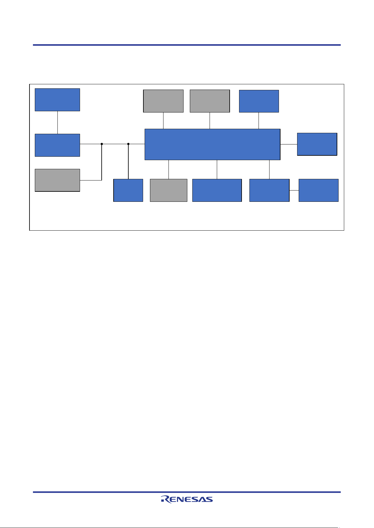
Target Board for RX23W 1. Overview
Evaluation MCU
USB
connector
External power
-
supply header
MCU
header x
2
Reset switch
User switch
User LED x
2
Main clock
Sub-
clock
Pmod™
connector
Arduino™
UNO
connector
Note: Gray shading of blocks indicates parts that are not mounted on the board.
USB
serial port
Power
indicator
LED
USB
connector
BLE
a
ntenna
Emulator
circuit
1.6 Block Diagram
Figure 1-1 shows the block diagram of this product.
Figure 1-1 Block Diagram
R20UT4634EJ0102 Rev.1.02 Page 9 of 33
Nov.27.19
Page 10
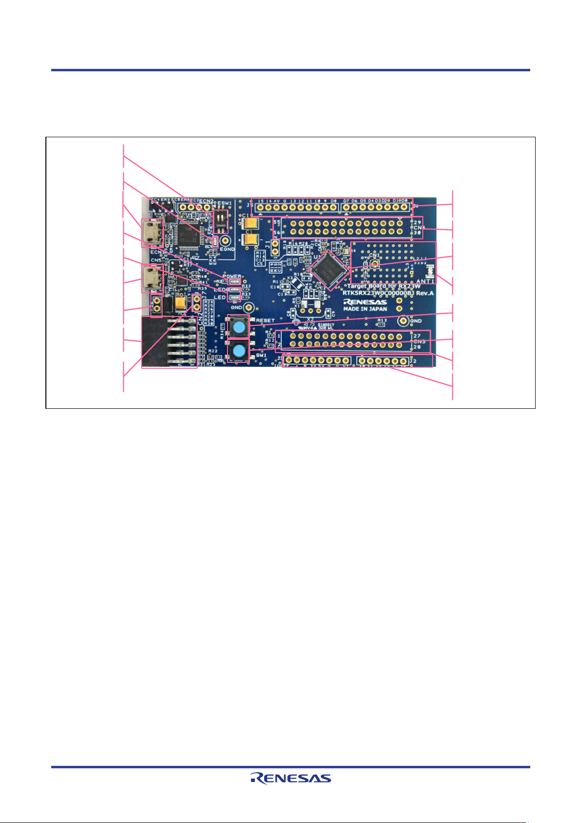
Target Board for RX23W 2. Board Layout
MCU headers
Reset switch
User switch
Pmod
TM
connector
Evaluation
MCU
ACT LED
Emulator
reset switch
USB connector
(
USB
s
erial
)
External power-
supply header
Power indicator
LED
Current
measurement
header
USB connector
(
e
mulator)
Arduino™ UNO
headers
Arduino™ UNO
headers
MCU headers
RF block
User LED
2. Board Layout
Figure 2-1 shows the external appearance of the top side of this product.
Figure 2-1 Board Layout (Top Side)
R20UT4634EJ0102 Rev.1.02 Page 10 of 33
Nov.27.19
Page 11

Target Board for RX23W 3. Parts Layout
90.
0
mm
54.0mm
33.02mm 2.54mm
2.54mm
3. Parts Layout
Figure 3-1 shows the parts layout of this product.
Figure 3-1 Parts Layout
R20UT4634EJ0102 Rev.1.02 Page 11 of 33
Nov.27.19
Page 12

Target Board for RX23W 4. Operating Environment
Host PC
USB cable
Target Board for RX23W
4. Operating Environment
Figure 4-1 shows the operating environment of this product. Install the IDE from the following URL on the host
PC. The installer automatically installs all required drivers along with the IDE.
https://www.renesas.com/development-tools
Figure 4-1 Operating Environment
R20UT4634EJ0102 Rev.1.02 Page 12 of 33
Nov.27.19
Page 13

Target Board for RX23W 5. User Circuits
Note:
5. User Circuits
5.1 Evaluation MCU
The MCU specifications for the power supply, system clock, and reset at the time of shipment are as follows.
• Power supply: Fixed 3.3 V (including the analog power supply)
• System clock: Operation with an on-chip oscillator
• Reset: Directed by the reset switch or IDE
5.2 Bluetooth Low Energy
A BLE communications circuit is mounted on this board.
Figure 5-1 BLE Circuit
Never remodel the BLE circuit, as doing so will violate radio-related laws.
R20UT4634EJ0102 Rev.1.02 Page 13 of 33
Nov.27.19
Page 14

Target Board for RX23W 5. User Circuits
Emulator reset
switch (ESW1)
OFF
ON
ESW1
Function
MCU
Channel 2
Resets the emulator.
Off
The emulator is reset.
5.3 Emulator
An emulator is mounted on the board. With the settings as shipped, the switches shown in Figure 5-2 are
turned off and the emulator is in reset state. To use the emulator, make the corresponding switch setting in
Table 5-1.
The shape of the emulator connector (ECN1) is USB micro-B for the IDE and for the Renesas Flash
Programmer (RFP). Connect the emulator connector to the computer by a USB cable. If the power supply on
the host side is on, the power is supplied to this product at the same time as connection of the cable.
Note: The package does not include a USB cable.
Figure 5-2 Emulator Reset Switch (ESW1)
Table 5-1 Setting of the Emulator Reset Switch (ESW1)
Channel 1 Not used.
On The emulator can be used.
The emulator cannot be used.
R20UT4634EJ0102 Rev.1.02 Page 14 of 33
Nov.27.19
Page 15

Target Board for RX23W 5. User Circuits
Signal Name
Function and Usage
MCU
Port
Pin
RXD
Signal for receiving data
PC6
24
CTS
Input signal for controlling the start of transmission and reception of data
*1
5.4 USB-to-Serial Conversion
USB connector CN5 is connected to the USB-to-serial conversion module from FTDI and can be used as a
virtual COM port. Table 5-2 shows the connection relationship of USB-to-serial signals.
Table 5-2 Names of the USB-to-Serial Signals
TXD Signal for transmitting data PC7 23
RTS Output signal for controlling the start of transmission and reception of data *1
Note: This port is not connected on the board as shipped.
The first time the CPU board is connected to the USB port of a PC, the monitor of the PC shows the message
stating that installation of the driver is in progress as shown in Figure 5-3. After that, a message indicating
completion of the driver installation is displayed. The content of the message will differ with the OS version on
the host PC.
Figure 5-3 Displays Indicating Installation of the USB-to-Serial Driver
If you do not have a driver, download the installer for the driver from the Web site of FTDI.
5.5 ACT LED
The ACT LED displays the state of operation of the emulator control software. The illumination conditions are
listed below. The LED is green.
• Illuminated: Indicates that the emulator is connected to the target.
• Blinking: Indicates that the host machine (PC) has recognized the emulator.
• Not illuminated: Indicates that the emulator cannot be used for some reason (including its power being off).
5.6 Power LED
While the power LED is illuminated, power is being supplied to the board. The LED is green.
5.7 User LEDs
The optional user LEDs can be used for any purpose. LED0 and LED1 are mounted on the board and are
respectively connected to the following ports. The LEDs are green.
• LED0: Pin 30, connected to port PC0
• LED1: Pin 35, connected to port PB0
R20UT4634EJ0102 Rev.1.02 Page 15 of 33
Nov.27.19
Page 16

Target Board for RX23W 5. User Circuits
Pattern for
cutting (SS19)
External power
supply header
(J6)
5.8 External Power-Supply Header
When more current is required than the USB is capable of supplying, use the external power-supply header
(J6) to supply power. The usable voltage is 3.3 V. When this header is to be used, remove the pattern for
cutting (SS19) on the soldered side, electrically separating the emulator from the target. Figure 5-4 shows the
position of the pattern for cutting. Figure 5-5 shows the position of the external power-supply header (the
actual header component is not mounted on the board as shipped).
Figure 5-4 Position of the Pattern for Cutting (SS19) (Soldered Side)
R20UT4634EJ0102 Rev.1.02 Page 16 of 33
Nov.27.19
Figure 5-5 Position of the External Power-Supply Header (J6) (Top Side)
Page 17

Target Board for RX23W 5. User Circuits
Pin No.
Signal Name
Evaluation MCU
Pin No.
Signal Name
Evaluation MCU
Port
Pin
Port
Pin
3
PMOD1-MISO
P30
12 9 PMOD1-IO0
P05 (PC2)
55 (29)
4
PMOD1-SCK
P27
13
10
PMOD1-IO1
PB7 (PC3)
31 (27)
Pmod
RX23W
P05
Pin 9
CN4-7
Arduino
Pin 10
PB7
PC2 [RxD5]
PC3 [TxD5]
PC2 [RxD5]
PC3 [TxD5]
P05
PB7
CN4-8
5.9 Pmod Connector
A Pmod connector (CN2) is connectable to the evaluation MCU via a type 2A Pmod interface. Note that
the pin assignments of the Pmod connector differ from those of other headers. Figure 5-6 and Table 5-3
show the pin assignments of the Pmod connector and the specifications of signals on the Pmod connector,
respectively. The IRQ4 interrupt is multiplexed on the same pin.
Figure 5-6 Pin Assignments of the Pmod Connector (Top View)
Table 5-3 Pin Assignments of the Pmod Connector
1 PMOD1-CS P31 11 7 PMOD1-IRQ PB1 33
2 PMOD1-MOSI P26 14 8 PMOD1-RST PD3 47
5 GROUND 11 GROUND
6 TARGET_VCC 12 TARGET_VCC
Figure 5-7 Pmod Multi-Function Pins
R20UT4634EJ0102 Rev.1.02 Page 17 of 33
Nov.27.19
Page 18

Target Board for RX23W 5. User Circuits
Pin No.
Signal Name
Specification
MCU
1
A0
AD input
AN001
51 2 A1
AN005
50
5
A4
AN018
43 6 A5
AN019
42
Pin No.
Signal Name
Specification
MCU
Signal Name
Pin No.
2
IOREF
IOREF
VCC 3 RESET
RESET
RES#
5 4 3V3
Power supply
VCC
7
GND
GND 8 VIN
VCC
5.10 Arduino UNO Headers
For the J2, J3, J4, and J5 headers, through holes are assigned with a pitch of 2.54 mm and these headers
are connected to the evaluation MCU according to the Arduino UNO R3 specification. Table 5-4, Table 5-5,
Table 5-6, and Table 5-7 show the signal specifications of the Arduino UNO connectors (the actual
connector components are not mounted on the board as shipped).
Table 5-4 Pin Assignments of J2 (6-Pin Analog Connector)
Signal Name Pin No.
3 A2 AN006 49
4 A3 AN007 48
Table 5-5 Pin Assignments of J3 (8-Pin Power Connector)
1 Reserved Reserved
5 5V
6 GND GND
R20UT4634EJ0102 Rev.1.02 Page 18 of 33
Nov.27.19
Page 19

Target Board for RX23W 5. User Circuits
Pin No.
Signal Name
Specification
MCU
8
D0/RX
GPIO/RxD
PC2/RxD5
29 7 D1/TX
GPIO/TxD
PC3/TxD5
27
4
D4/INT
GPIO/IRQ
PB1/IRQ4
33 3 D5/PWM/INT
GPIO/PWM/IRQ
P14/MTIOC3A/IRQ4
18 2 D6/PWM
GPIO/PWM
PE4/MTIOC4D
41
Pin No.
Signal Name
Specification
MCU
Signal Name
Pin No.
9
D9/PWM
GPIO/PWM
PC6/MTIOC3C
24 8 D10/PWM
GPIO/PWM
PC5/MTIOC3B
25 7 D11/MOSI/PWM
GPIO/PWM
P26/SMOSI1/MTIOC2A
14
3
ADREF
ADREF
2 SDA
II2 data
SDA
15
Table 5-6 Pin Assignments of J4 (8-Pin Digital Connector)
Signal Name Pin No.
6 D2 GPIO PC0 30
5 D3/PWM/INT GPIO/PWM/IRQ PB7/MTIOC3B 31
1 D7 GPIO PB0 35
Table 5-7 Pin Assignments of J5 (10-Pin Digital Connector)
10 D8 GPIO P31 11
6 D12/MISO GPIO P30/SMISO1 12
5 D13/SCK GPIO P27/SCK1 13
4 GND GND
1 SCK II2 clock SCL 16
R20UT4634EJ0102 Rev.1.02 Page 19 of 33
Nov.27.19
Page 20

Target Board for RX23W 5. User Circuits
Current
measurement
header (J7)
Pattern for
cutting (SS20)
5.11 Current Measurement Header
The current measurement header (J7) is used to measure the current drawn by the evaluation MCU (an actual
header component is not mounted on the board as shipped). The current drawn can be measured by
connecting an ammeter to the evaluation MCU. When this header is to be used, remove the relevant pattern
for cutting (SS20) on the soldered side. Figure 5-8 shows the positions of the header and pattern for cutting.
5.12 MCU Headers
MCU headers are provided for by two sets of through holes (CN3 and CN4) for 28-pin headers (actual header
components are not mounted on the board as shipped). The pin headers have a pitch of 2.54 mm and are
connected to the evaluation MCU. Pin numbers of the MCU headers correspond to those of the evaluation
MCU, and most pins are connected (with pins 1, 3, 4, 19, 22, 28, 32, 37, 38, 39, 40, 44, 45, and 46 as the
exceptions).
5.13 Reset Switch
Pressing the RESET switch applies a hardware reset to the evaluation MCU.
5.14 User Switch
An optional user switch (SW1) is mounted. It is connected to pin 17 of the evaluation MCU, which operates as
pin function P15. The IRQ5 interrupt is multiplexed on the same pin.
5.15 Patterns for Cutting
Patterns must be cut or repaired by soldering if necessary. Figure 5-9 shows examples of the states of
patterns for cutting.
Figure 5-8 Positions of the Current Measurement Header (J7) and Pattern for Cutting (SS20)
(Soldered Side)
R20UT4634EJ0102 Rev.1.02 Page 20 of 33
Nov.27.19
Page 21

Target Board for RX23W 5. User Circuits
Soldered
Connected Removed
Restored by soldering
Figure 5-9 Examples of States of Patterns for Cutting
R20UT4634EJ0102 Rev.1.02 Page 21 of 33
Nov.27.19
Page 22

Target Board for RX23W 6. Configurations
When removing soldered components, do not apply a soldering iron to the Target Board for RX23W for more than 5
Analog Power-Supply Source of
Mounted
Not Mounted
Remark
3.3 V on the board
R15, R19
R16, R18
MCU headers
R16, R18
R15, R19
A bypass capacitor (C13) becomes ineffective.
Reference Power-Supply Source
Mounted
Not Mounted
Remark
6. Configurations
6.1 Modifying the Target Board for RX23W
This section describes how to change the setting of this product by using option-link resistors.
An option-link resistor is a 0-Ω surface-mount resistor, which is used to short-circuit or isolate a part of circuits.
The subsequent sections contain lists of option-link resistors for individual functions. Fit or remove option-link
resistors to switch functions with reference to the list. Resistor numbers in bold blue type indicate the initial
state of the configuration on the Target Board for RX23W as shipped. For the positions of the option links,
refer to chapter 3, Parts Layout.
seconds. This time restriction is to avoid any damage components mounted nearby on the board.
6.2 Analog Power Supply
Table 6-1 and Table 6-2 show the option-link resistors for the analog power supply.
Table 6-1 Option-Link Resistors for the Analog Power Supply of the 12-Bit A/D and 12-Bit D/A
Converters
the 12-Bit A/D and 12-Bit D/A
Converters
Table 6-2 Option-Link Resistors for the Reference Power Supply of the 12-Bit A/D Converter
of the 12-Bit A/D Converter
3.3 V on the board R14, R17 R20, R21
MCU headers R20, R21 R14, R17 A bypass capacitor (C12) becomes ineffective.
R20UT4634EJ0102 Rev.1.02 Page 22 of 33
Nov.27.19
Page 23

Target Board for RX23W 6. Configurations
Setting of the HOCO
Mounted
Not Mounted
Remark
Oscillating
R5, R9
R6, R8
Halted
R6, R8
R5, R9
Mount a crystal oscillator on X1 or X2 and the
Setting of the LOCO
Mounted
Not Mounted
Remark
6.3 On-Chip Oscillator
Table 6-3 and Table 6-4 show the option-link resistors for the operation of the on-chip oscillator.
Table 6-3 Option-Link Resistors for the HOCO
load capacitance as C8 or C9.
Table 6-4 Option-Link Resistors for the LOCO
Oscillating R11
Halted R11
Mount a crystal oscillator on X3 and the load
capacitance as C10 or C11.
R20UT4634EJ0102 Rev.1.02 Page 23 of 33
Nov.27.19
Page 24

Target Board for RX23W 7. Handling Precautions
7. Handling Precautions
7.1 Adding Load
When load is added while power is being supplied via the USB, the maximum current is 300 mA during
operation at 3.3 V.
When load is added while power is being supplied externally, the maximum current is 500 mA regardless of
the operating voltage.
7.2 Remodeling the Board
Any modification of the board (including removing the patterns for cutting) shall be conducted at the user’s
own responsibility.
7.3 Limitation on the Number of Connected Target Boards for RX23W
Connecting the same host PC to multiple Target Boards for RX23W is not possible.
R20UT4634EJ0102 Rev.1.02 Page 24 of 33
Nov.27.19
Page 25

Target Board for RX23W 8. Developing Code
8. Developing Code
8.1 Using the e2 studio
Figure 8-1 shows the settings of the e2 studio when creating a new project for the Target Board for RX23W.
• [Debug hardware]: Select [E2 Lite (RX)].
• [Power Target From The Emulator]: Select [No].
• [Flash ID Code]: Enter [45FFFFFFFFFFFFFFFFFFFFFFFFFFFFFF].
Figure 8-1 Settings of the e2 studio
Note: Do not connect another Target Board for RX23W to your PC while this product is already connected.
R20UT4634EJ0102 Rev.1.02 Page 25 of 33
Nov.27.19
Page 26

Target Board for RX23W 8. Developing Code
8.2 Using CS+
Figure 8-2 and Figure 8-3 show the settings of CS+ when creating a new project for the Target Board for
RX23W.
• [Using Debug Tool]:
Select [RX E2 Lite] from [Using Debug Tool] in the [Debug] menu.
Figure 8-2 Panel for Selecting the Debug Tool
• [Power target from the emulator]: Select [No].
• [Flash ID Code]: Enter [45FFFFFFFFFFFFFFFFFFFFFFFFFFFFFF].
Figure 8-3 [Connect Settings] Tabbed Page of CS+
R20UT4634EJ0102 Rev.1.02 Page 26 of 33
Nov.27.19
Page 27

Target Board for RX23W 9. Additional Information
9. Additional Information
Technical Support
For details on the RX23W-group microcontrollers, refer to the RX23W Group User’s Manual: Hardware.
For details on the RX assembly language, refer to the RX Family User’s Manual: Software.
The latest information is available from this Web page: https://www.renesas.com/rxtb
Technical Contact Details
America: techsupport.america@renesas.com
Europe: https://www.renesas.com/en-eu/support/contact.html
Global & Japan: https://www.renesas.com/support/contact.html
General information on Renesas microcontrollers can be found on the Renesas website at:
https://www.renesas.com/
Note
Do not install the Target Board for RX23W or sample code into your product.
The operation of sample code is not guaranteed. Confirm the operation on your own responsibility.
.
Trademarks
All brand or product names used in this manual are trademarks or registered trademarks of their respective
companies or organisations.
Copyright
This document may be, wholly or partially, subject to change without notice. All rights reserved. Duplication of
this document, either in whole or part is prohibited without the written permission of Renesas Electronics
Europe Limited.
© 2019 Renesas Electronics Corporation. All rights reserved.
R20UT4634EJ0102 Rev.1.02 Page 27 of 33
Nov.27.19
Page 28

Target Board for RX23W 10. Certification of Compliance
10. Certification of Compliance
The Target Board for RX23W complies with the laws and regulations described below.
10.1 Radio-Related Laws
Japan: Type certification (authentication number: 001-P01398)
Europe: CE (RE)
North America: FCC (FCC ID: 2AEMXRX23WTBQ56), ISED (20194-RX23WTBQ56)
RE Directive
Hereby, Renesas Electronics Corporation declares that the radio equipment type RTK5RX23W0C00000BJ is
in compliance with Directive 2014/53/EU.
R20UT4634EJ0102 Rev.1.02 Page 28 of 33
Nov.27.19
Page 29

Target Board for RX23W 10. Certification of Compliance
FCC/ISED Regulatory
Since this module is not sold to general end users directly, there is no user manual of module.
For the details about this module, please refer to the specification sheet of module.
This module should be installed in the host device according to the interface specification (installation
procedure).
The following information must be indicated on the host device of this module;
FCC ID: 2AEMXRX23WTBQ56
This device complies with part 15 of the FCC Rules. Operation is subject to the following two conditions: (1)
This device may not cause harmful interference, and (2) this device must accept any interference received,
including interference that may cause undesired operation.
IC: 20194-RX23WTBQ56
[for FCC]
FCC CAUTION
Changes or modifications not expressly approved by the party responsible for compliance could void the
user’s authority to operate the equipment.
This transmitter must not be co-located or operated in conjunction with any other antenna or transmitter.
This equipment complies with FCC radiation exposure limits set forth for an uncontrolled environment and
meets the FCC radio frequency (RF) Exposure Guidelines. This equipment has very low levels of RF energy
that it deemed to comply without maximum permissive exposure evaluation (MPE). But it is desirable that it
should be installed and operated keeping the radiator at least 20cm or more away from person's body.
This device complies with FCC Part 15.203 because the antenna is not removable from this device.
[for ISED]
This device complies with Industry Canada's licence-exempt RSSs. Operation is subject to the following two
conditions: (1) This device may not cause interference; and (2) This device must accept any interference,
including interference that may cause undesired operation of the device.
Le présent appareil est conforme aux CNR d’Industrie Canada applicables aux appareils radio exempts de
licence. L’exploitation est autorisée aux deux conditions suivantes : 1) l’appareil ne doit pas produire de
brouillage; 2) l’utilisateur de l’appareil doit accepter tout brouillage radioélectrique subi, même si le brouillage
est susceptible d’en compromettre le fonctionnement.
This equipment complies with IC radiation exposure limits set forth for an uncontrolled environment and meets
RSS-102 of the IC radio frequency (RF) Exposure rules. This equipment has very
R20UT4634EJ0102 Rev.1.02 Page 29 of 33
Nov.27.19
Page 30

Target Board for RX23W 10. Certification of Compliance
low levels of RF energy that it deemed to comply without maximum permissive exposure evaluation (MPE).
But it is desirable that it should be installed and operated keeping the radiator at least 20cm or more away
from person's body.
Cet équipement est conforme aux limites d’exposition aux rayonnements énoncées pour un environnement
non contrôlé et respecte les règles d’exposition aux fréquences radioélectriques (RF) CNR-102 de l’IC. Cet
équipement émet une énergie RF très faible qui est considérée conforme sans évaluation de l’exposition
maximale autorisée. Cependant, il est souhaitable qu'il devrait être installé et utilisé en gardant une distance
de 20 cm ou plus entre le radiateur et le corps humain.
HVIN and PMN of this product is “RTK5RX23W0C00000BJ”.
R20UT4634EJ0102 Rev.1.02 Page 30 of 33
Nov.27.19
Page 31

Rev.
Date
Description
Page
Summary
1.01
Nov.01.19
P4
Update the Document Title of Application note.
1.02
2019.11.27
P29,30
Update FCC/ISED Regulatory
Revision History Target Board for RX23W User’s Manual
1.00 Oct.01.19 First Edition issued
P25,26 Added Flash ID Code setting.
Page 32

Published by: Renesas Electronics Corporation
Target Board for RX23W User’s Manual
Publication Date: Rev.1.02 Nov.27.19
Page 33

roup
R20UT4634EJ0102
RX23W G
 Loading...