

Page 1

Application Note
RSSKRX23E-A
PC Tool Program Operation Manual
Introduction
This document is an operation manual of the PC tool program (called the PC tool below) that is connected to
the Renesas Solution Starter kit for RX23E-A (called RSSKRX23E-A below) board for operation. For details
on the MCU, refer to " RX23E-A Group User’s Manual: Hardware ".
The PC tool is used in combination with the included firmware for RX23E-A.
Target Device
RSSKRX23E-A board
Contents
1. Overview ................................................................................................................................. 3
1.1 System Overview ..................................................................................................................................... 3
1.2 Operating Environment ........................................................................................................................... 4
1.3 Conditions for Operation Confirmation .................................................................................................... 4
1.4 File Configuration .................................................................................................................................... 4
1.5 Installation and Uninstallation .................................................................................................................. 4
1.5.1 Installation and Execution ..................................................................................................................... 4
1.5.2 Uninstallation ......................................................................................................................................... 4
1.6 Modification from the previous version. ................................................................................................... 5
1.7 Reference Documents ............................................................................................................................. 5
2. Explanation of Functions ......................................................................................................... 6
2.1 Menu Bar ................................................................................................................................................. 7
2.2 Operation Buttons.................................................................................................................................... 7
2.2.1 Connection ............................................................................................................................................ 8
2.2.2 Calibration ............................................................................................................................................. 9
2.3 WaveForm Tab ...................................................................................................................................... 10
2.3.1 Graphical Display Area ........................................................................................................................ 10
2.3.2 Operation Buttons ............................................................................................................................... 11
2.3.3 Setting Area ......................................................................................................................................... 12
2.4 Histogram Tab ....................................................................................................................................... 13
2.4.1 Graphical Display Area ........................................................................................................................ 13
2.4.2 Operation Buttons ............................................................................................................................... 14
2.4.3 Setting Area ......................................................................................................................................... 15
2.5 Registers Tab ........................................................................................................................................ 16
2.5.1 AFE and DSAD Block Diagram ........................................................................................................... 17
2.5.2 Operation Buttons ............................................................................................................................... 18
2.5.3 Register Value Displaying Area ........................................................................................................... 18
R20AN0540EJ0201 Rev.2.01 Page 1 of 39
March 15.21
Page 2

RSSKRX23E-A PC Tool Program Operation Manual
2.6 SINC4 Tab ............................................................................................................................................. 19
2.6.1 Operation Buttons ............................................................................................................................... 20
2.6.2 SINC4 Filter Frequency-Gain Characteristic Graph ............................................................................ 20
2.6.3 Setting Area ......................................................................................................................................... 21
2.7 Application Tab ...................................................................................................................................... 22
2.7.1 Graphical Display Area ........................................................................................................................ 22
2.7.2 Operation Buttons ............................................................................................................................... 23
2.7.3 Setting Area ......................................................................................................................................... 24
3. File Specification ................................................................................................................... 25
3.1 Configuration File .................................................................................................................................. 25
3.2 A/D Conversion Value File .................................................................................................................... 27
3.3 Register Setting File .............................................................................................................................. 28
3.4 Measurement Value File ....................................................................................................................... 30
4. Communication Specification ................................................................................................. 31
4.1 Serial Communication Settings ............................................................................................................. 31
4.2 Sequence .............................................................................................................................................. 31
4.3 Packet Structure .................................................................................................................................... 32
4.4 Commands ............................................................................................................................................ 33
4.4.1 Negotiation .......................................................................................................................................... 33
4.4.2 Read .................................................................................................................................................... 34
4.4.3 Write .................................................................................................................................................... 34
4.4.4 Run ...................................................................................................................................................... 34
4.4.5 Stop ..................................................................................................................................................... 34
4.4.6 Data Transmission .............................................................................................................................. 35
4.4.6.1 Rev.1.0 .............................................................................................................................................. 35
4.4.6.2 Rev.2.0 .............................................................................................................................................. 35
4.4.7 Extra Information (Rev.2.0) ................................................................................................................. 35
Revision History ............................................................................................................................ 36
R20AN0540EJ0201 Rev.2.01 Page 2 of 36
March 15.21
Page 3
RSSKRX23E-A PC Tool Program Operation Manual
1. Overview
1.1 System Overview
This PC tool performs serial communication with the RSSKRX23E-A board (called the EVB below) by USB
connection to set the registers of the AFE and DSADs of RX23E-A on the board, control operation of the
AFE and DSADs, and obtain and display A/D conversion values for up to twelve channels. In addition, the
PC tool obtains and displays measurement values of the sample programs in the measurement example
application notes.
The main functions are listed below.
(1) Performs the following operations with serial communication through the EVB by USB connection.
・ Checks the connection with the EVB.
・ Obtains and sets RX23E-A register values.
・ Requests the EVB to start and stop A/D conversion.
・ Obtains A/D conversion values. (A/D conversion performs the continuous scan mode)
(2) Analyzes and displays the obtained A/D conversion values as follows.
・ Displays a waveform of the A/D conversion values.
・ Analyzes and displays a histogram of the A/D conversion values.
・ Displays various measurement results.
(3) Obtains and sets AFE and DSAD register setting values.
・ Selects and specifies register parameters in a block diagram.
・ Displays the register setting values for parameters.
Displays a SINC4 filter frequency-gain characteristic graph based on register setting values.
Figure 1-1 PC Tool Program
R20AN0540EJ0201 Rev.2.01 Page 3 of 36
March 15.21
Page 4
RSSKRX23E-A PC Tool Program Operation Manual
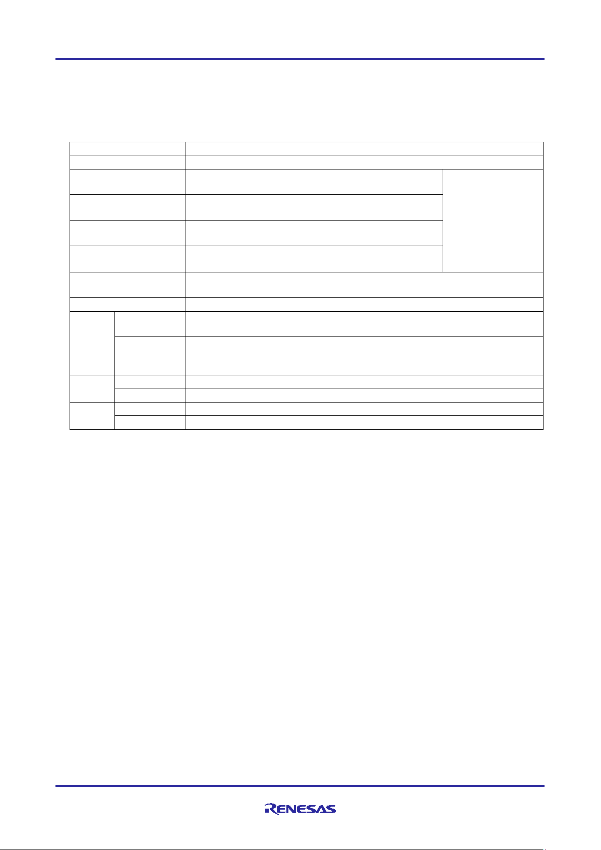
Item
Details
Evaluation board
RSSKRX23E-A board RTK0ESXB10C00001BJ
PC
CPU
Intel Core i5-6300U @ 2.40 GHz
Memory
8.00 GB
OS
Microsoft Windows 10 64-bit 1083
.NET Framework 4.7.2
File name
Explanation
RSSK23EA.exe
PC tool executable file
rx23ea_rssk_fw.mot
Firmware for RX23E-A (Motorola-S format)
This document
1.2 Operating Environment
・ OS: Microsoft Windows 10 (32/64 bits)
・ .NET Framework 4.7.2
1.3 Conditions for Operation Confirmation
The operation of this PC tool has been confirmed under the following conditions.
able 1-1 Conditions for Operation Confirmation
T
1.4 File Configuration
The file configuration of this PC tool is as follows.
Table 1-2 File Configuration
r20an0540ej0201-rsskrx23e-a.pdf
Note: The PC tool is used in combination with the included firmware for RX23E-A.
1.5 Installation and Uninstallation
1.5.1 Installation and Execution
To operate the PC tool, the following items may be required.
• USB Serial Port driver
On the EVB, FTDI USB serial conversion IC FT232 is mounted. If the system requests the driver o
onnecting the EVB with USB, download the driver file from the FTDI website (http://www.ftdichip.com/
c
and install it.
• Microsoft .NET Framework
If the PC tool does not start, download .NET Framework version 4.7.2 or later from the Microsoft website
and install it.
No special procedure is required for installing the PC tool. Execute the executable file stored on the PC.
1.5.2 Uninstallation
Delete the executable file and configuration file (RSSK23EA.ini).
n
)
R20AN0540EJ0201 Rev.2.01 Page 4 of 36
March 15.21
Page 5

RSSKRX23E-A PC Tool Program Operation Manual
1.6 Modification from the previous version.
Major modification from Version 1.0 is listed below.
(1) WaveForm Tab
・ Simultaneous display of multiple channel waveform
・ Channel selection display in Dump Dialog
・ The update of A/D conversion value file format and the readout of the previous version file.
(2) Histogram Tab: Specification change to support the channel function
・ Addition of selection function for histogram display.
・ Change of Bin value in Dump Dialog to median of each Bin.
(3) Registers Tab
・ Support the channel function.
・ Addition of the readout function for the built-in temperature sensor coefficient.
(4) Application Tab: Function enhancement to support up to 12chs.
・ Simultaneous display of waveform for up to 12chs.
・ Support time axis which is the horizontal axis of the graph (depending on information from FW)
・ Display of channel selection of Dump Dialog
・ The update of the measurement value file format and the readout of the previous version file.
(5) Others
・ Modification to the calibration per channel to support the channel function.
: WaveForm Tab : Function enhancement to support the channel function.
・ Addition of the register to support the register setting file.
・ Enhancement of the communication specifications
1.7 Reference Documents
• R20UT4542 RSSKRX23E-A User's Manual
• R01UH0801 RX23E-A Group User's Manual: Hardware
• R01AN4747 Application Note RX23E-A Group Example of Temperature Measurement using
Thermocouple
• R01AN4788 Application Note RX23E-A Group Example of Temperature Measurement using Resistance
Temperature Detector
• R01AN4789 Application Note RX23E-A Group Example of Weight Measurement using Load Cell
R20AN0540EJ0201 Rev.2.01 Page 5 of 36
March 15.21
Page 6
RSSKRX23E-A PC Tool Program Operation Manual
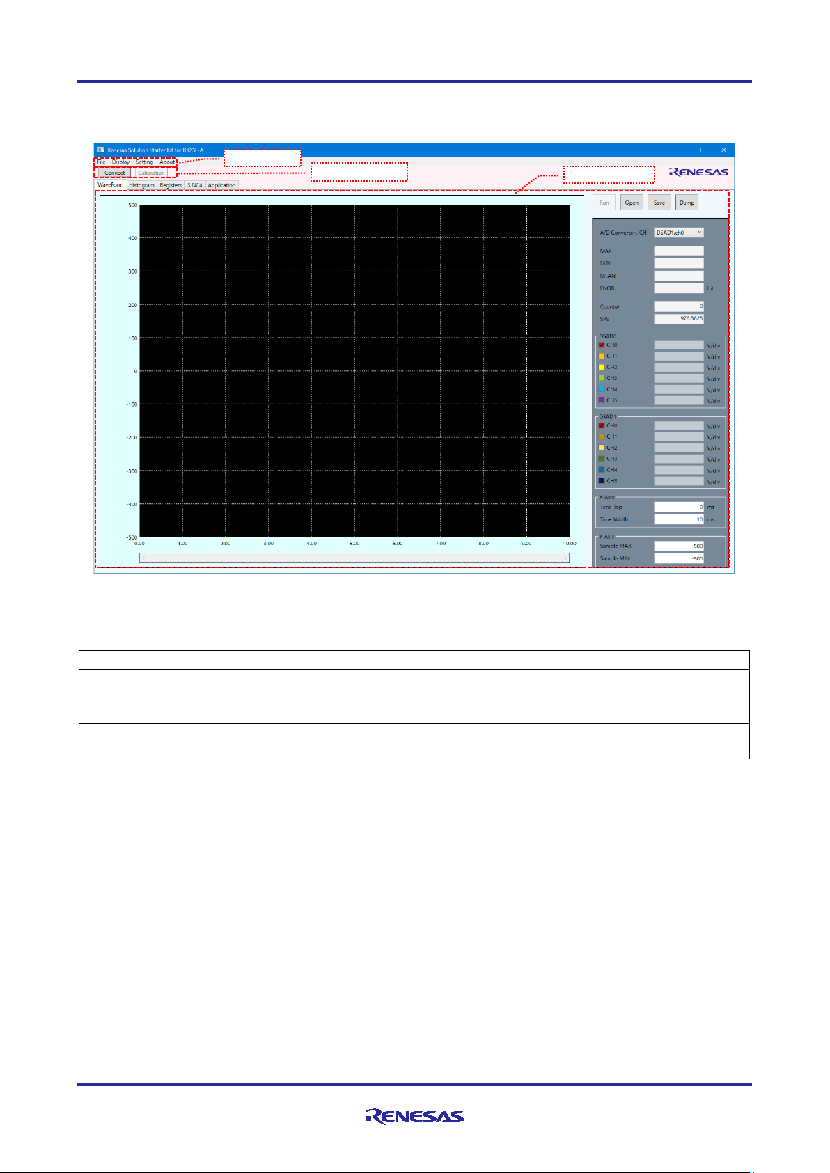
Item/area name
Explanation
Menu bar
There are four menus: "File", "Display", "Setting", and "About".
Operation buttons
The "Connect/Disconnect" and "Calibration" buttons are provided, which are
independent of the functions of each tab.
Function screen
Five function screens, "WaveForm", "Histogram", "Registers", "SINC4" and
“Application”, are available. To display a desired screen, click the corresponding tab.
Menu bar
Operation button
Function screen
2. Explanation of Functions
The screen of the PC tool consists of three areas. Figure 2-1 and Table 2-1 show the screen configuration.
Table 2-1 Screen Items and Areas
Figure 2-1 Screen Configuration
R20AN0540EJ0201 Rev.2.01 Page 6 of 36
March 15.21
Page 7
RSSKRX23E-A PC Tool Program Operation Manual
Menu
Item
Explanation
File
Exit
Exits the application.
Display
WaveForm
Displays the WaveForm Tab.
Histogram
Displays the Histogram Tab.
Registers
Displays the Registers Tab.
SINC4
Displays the SINC4 Tab.
Application
Displays the Application Tab.
Setting
Connect/
Disconnect
Corresponds to the "Connect/Disconnect" button. Starts or ends serial
communication according to the conditions set in the "Configure" menu.
Calibration
Corresponds to the "Calibration" button. Performs calibration.
Configure
Displays the dialog box for setting communication with the EVB (selecting
a COM port and setting a baud rate).
About
Displays the version information in the dialog box.
Button
Explanation
Connect/
Connects or disconnects serial communication with the EVB according to the settings
Calibration
Performs calibration of DSAD.
2.1 Menu Bar
Select a menu item to manipulate a file, select a function, make settings, and display application information.
Table 2-2 explains menus and menu items.
Table 2-2 Items on the Menu Bar
2.2 Operation Buttons
Use the corresponding buttons to connect to the EVB and calibrate DSAD. Table 2-3 explains the buttons.
Table 2-3 Operation Buttons
Disconnect
made in the "Configure" menu.
R20AN0540EJ0201 Rev.2.01 Page 7 of 36
March 15.21
Page 8
RSSKRX23E-A PC Tool Program Operation Manual
RSSKRX23E-A EVB
RX23E-A
USB-
Emulator
USB I/F
UART
(3Mbps)
USB 2.0FS
PC Tool
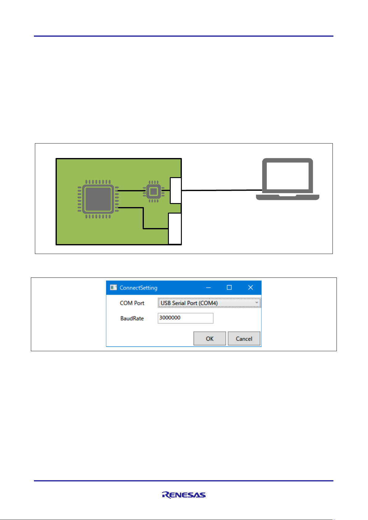
2.2.1 Connection
Follow the procedure below to establish a connection in order to operate the EVB from the PC Tool.
1. Connect the PC and EVB with a USB cable. Figure 2-2 shows a connection diagram. For details on
the board setting, refer to "RSSKRX23E-A User's Manual: Board".
2. Execute RSSK23EA.exe.
3. Select "Setting" > "Configure" from the menu bar to display the "ConnectSetting" dialog box (Figure
2-3).
4. Set communication-related items in the "ConnectSetting" dialog box.
"COM Port" combo box: Select a COM port used for communication.
"BaudRate" input field: Enter 3000000.
5. Click the "OK" button to close the "ConnectSetting" dialog box.
6. Click the "Connect" operation button to establish the connection.
Program
COM
I/F
Figure 2-2 System Connection Diagram
Figure 2-3 ConnectSetting Dialog Box
R20AN0540EJ0201 Rev.2.01 Page 8 of 36
March 15.21
Page 9
RSSKRX23E-A PC Tool Program Operation Manual
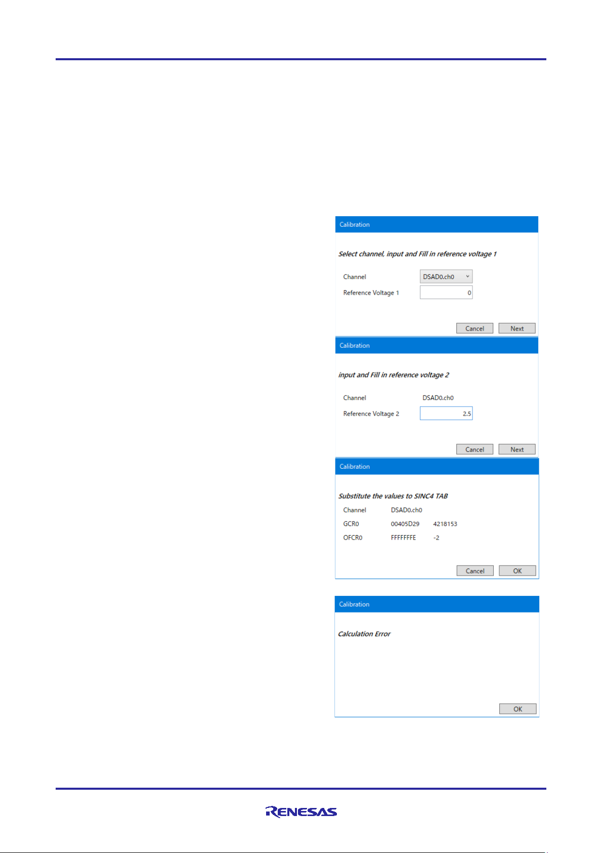
1.
After establishing a connection with the EVB, specify the register setting on Registers and SINC4
2.
Click the "Calibration" operation button to start the calibration procedure.
3.
In "Select channel, input and Fill in reference voltage
4.
Following "A/D value acquisition", "input and Fill in
5
Following "AD value acquisition / Calculation", the
If an error occurs in the calibration procedure,
2.2.2 Calibration
Use the "Calibration" button to calculate the values of the gain of the A/D conversion and offset correction
registers based on the A/D conversion result of two types of input voltage. The gain correction of the
calibration result contains the correction of digital filter gain depending on the SINC4 settings.
The Calibration performs for each channel of DSAD unit. Calibration can be performed interactively in the
displayed dialog box as follows:
Tabs according to the use conditions.
1", select a channel of DSAD unit for which to perform
calibration, enter the reference voltage 1 which inputs
to the pin, and click the "Next" button.
reference voltage 2", enter the reference voltage 2
which inputs to the pin and click the "Next" button.
calibration result appears.
Click the "OK" button to reflect the values in
"Gain/Offset Correction" on the SINC4 Tab and “CGR
and OFCR” on the Registers Tab.
To apply the values to the device, check the
checkboxes of GCR and OFCR, and click "Set" on
the Registers Tab.
Click the "Cancel" button to discard the calibration
result and terminate calibration.
"Calculation Error" appears.
R20AN0540EJ0201 Rev.2.01 Page 9 of 36
March 15.21
Page 10
RSSKRX23E-A PC Tool Program Operation Manual
1
2
3
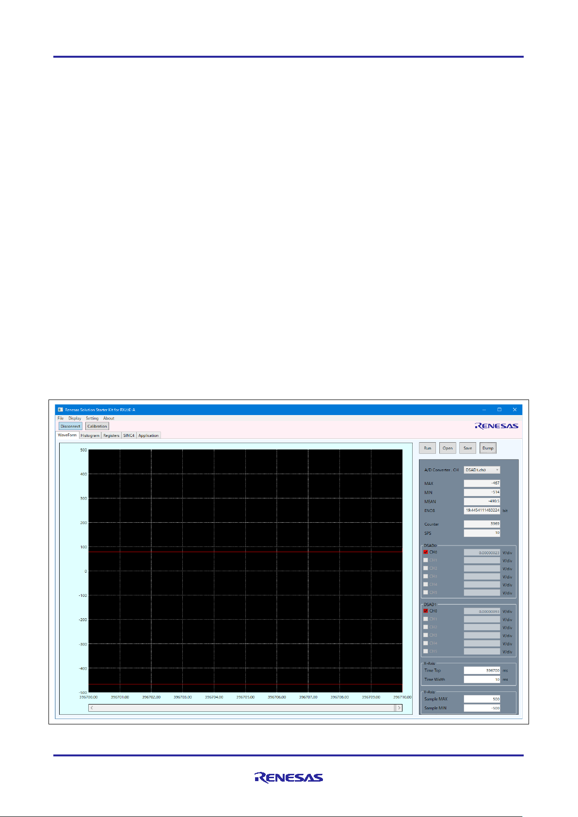
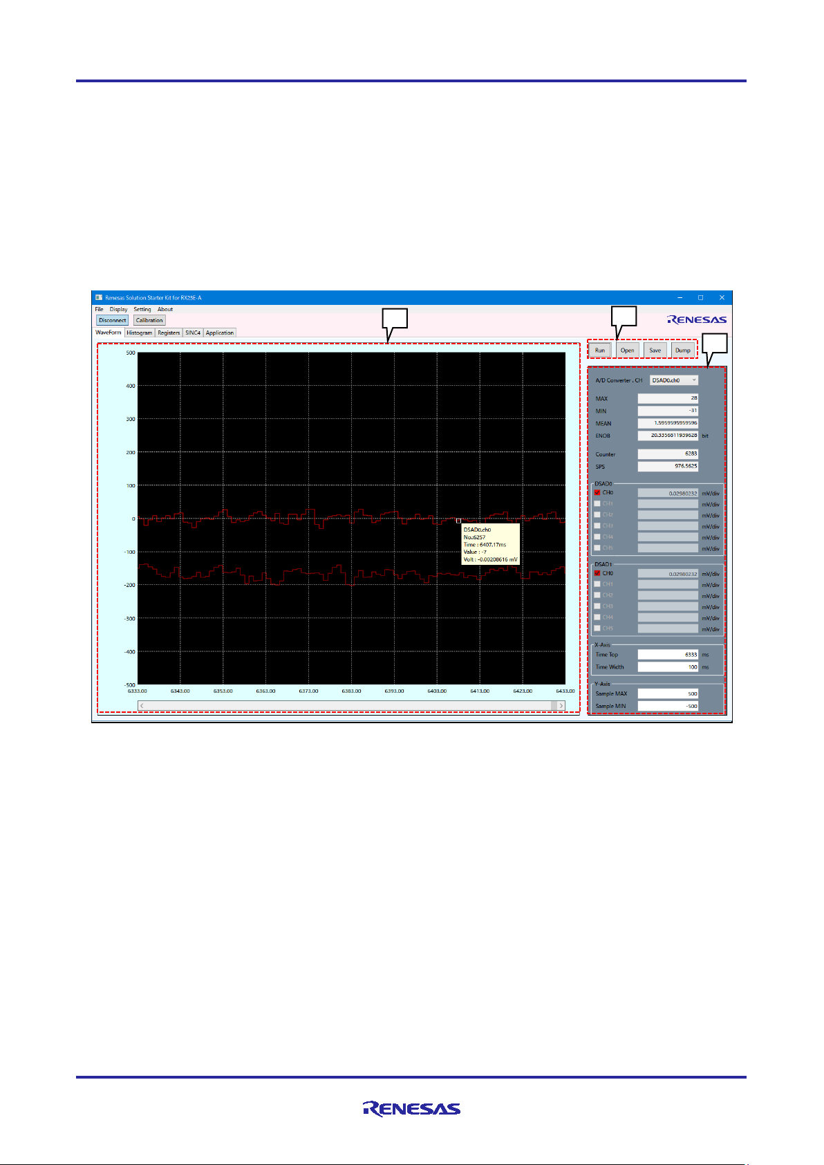
2.3 WaveForm Tab
WaveForm Tab obtains A/D conversion values from the EVB with serial communication and display a
waveform graph. In addition, it is possible to save the obtained A/D conversion values in a file, and read
saved A/D conversion values to display a graph.
A/D conversion values can be measured during up to 1 hour with the output data rate of 15625 SPS.
The WaveForm Tab consists of the following three areas as shown in Figure 2-4.
1. Graphical display area
2. Operation buttons
3. Setting area
Figure 2-4 WaveForm Tab Screen
2.3.1 Graphical Display Area
In this area, A/D conversion values are displayed as a waveform. The horizontal axis indicates the time, the
vertical axis indicates the conversion value. The value displayed on each axis depends on the settings in the
"X-Axis" or "Y-Axis" group in the setting area.
The graph is updated to the latest values when the scroll bar is positioned at the right end while A/D
conversion values are being obtained from the EVB.
Note: Display update may be suppressed to prioritize obtaining A/D conversion value. During suppression,
the graph and measurement value are not updated. Suppression condition can be specified by
“UpdateRestriction” parameter in the “WaveForm” section of the configuration file. Refer to “0
Configuration File” in detail.
R20AN0540EJ0201 Rev.2.01 Page 10 of 36
March 15.21
Page 11
RSSKRX23E-A PC Tool Program Operation Manual
Button
Explanation
Run/Stop
Obtains or stops A/D conversion values when the connection with the EVB is established.
the button"Run" will be displayed.
Open
Reads a saved A/D conversion value file. This button is disabled during A/D conversion.
When a saved file is read, the A/D conversion values being held are discarded.
Save
Saves all A/D conversion values being held in a file. This button is disabled during A/D
conversion.
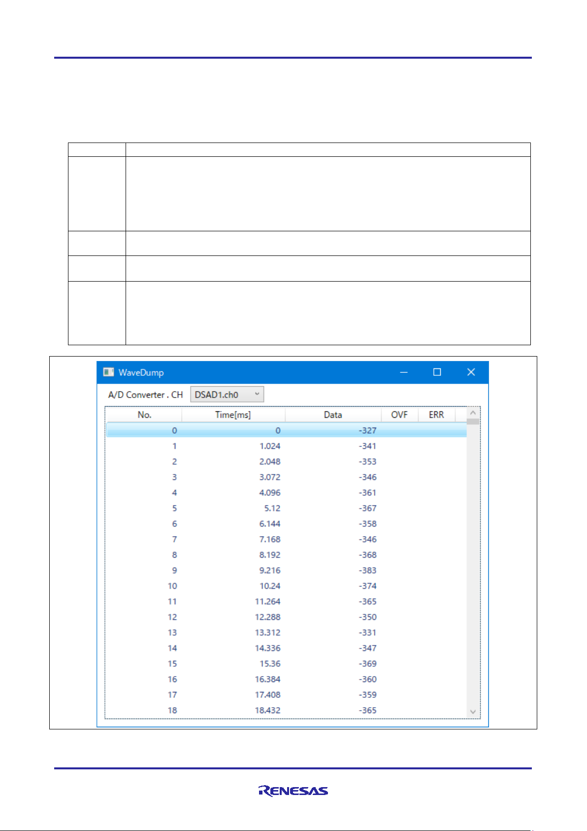
Dump
Displays a list of A/D conversion values of the channel of DSAD unit in the "WaveDump"
When this dialog box is open, the tabs cannot be switched.
2.3.2 Operation Buttons
Use the operation buttons to start and stop A/D conversion, save and read A/D conversion values from a file,
and display the conversion values in a list.
Table 2-4 explains the operation buttons.
Table 2-4 WaveForm Tab Operation Buttons
When "Run" is displayed on the button, clicking the button will start A/D conversion and
"Stop" button will be displayed. The obtained A/D conversion values are displayed in a
graph.
When "Stop" is displayed on the button, clicking the button will stop A/D conversion and
dialog box shown in Figure 2-5.The displayed channel of unit can be switched.
The list can be copied in range selection as the CSV format by using CTRL+C.
The dialog box cannot be opened during A/D conversion.
Figure 2-5 WaveDump Dialog Box
R20AN0540EJ0201 Rev.2.01 Page 11 of 36
March 15.21
Page 12
RSSKRX23E-A PC Tool Program Operation Manual
Item
Explanation
A/D Converter
Select the channel of DSAD unit for which to display A/D conversion values.
MAX
Displays the maximum A/D conversion value of the
selected channel of DSAD unit.
The display is
MIN
Displays the minimum A/D conversion value of the
MEAN
Displays the average A/D conversion value of the
selected channel of DSAD unit.
ENOB
Displays the ENOB of the A/D conversion values of the
Counter
Displays the number of all samples of A/D conversion values of the selected
channel of DSAD unit
SPS
Displays the data rate of the selected channel of DSAD unit.
DSAD0
CHm
(m=0 ~ 5)
Select the each DSAD channel which is displayed in the graph.
V/div
Displays the each DSAD channel voltage on the vertical axis with V/div. The
X-Axis
Time Top
Set the left limit of the horizontal axis of the displayed graph in milliseconds.
Time Width
Set the width of the horizontal axis of the displayed graph in milliseconds.
Y-Axis
Sample MAX
Set the maximum value of the vertical axis of the displayed graph in decimal.
Sample MIN
Set the minimum value of the vertical axis of the displayed graph in decimal.
2.3.3 Setting Area
Use the setting area to set items related to the graphical display and display various measurement values of
the A/D conversion values. Table 2-5 explains the items.
Table 2-5 WaveForm Tab Setting Area
stopped according
to the condition
selected channel of DSAD unit.
selected channel of DSAD unit.
DSAD1
during A/D
conversion
obtainment.
voltage is calculated from each voltage which is set at “Voltages” on the
Registers Tab.
R20AN0540EJ0201 Rev.2.01 Page 12 of 36
March 15.21
Page 13

RSSKRX23E-A PC Tool Program Operation Manual
1 2 3
2.4 Histogram Tab
Histogram Tab displays a histogram with the A/D conversion values displayed on the WaveForm Tab as a
population.
The Histogram Tab consists of the following three areas as shown in Figure 2-6.
1. Graphical display area
2. Operation buttons
3. Setting area
Figure 2-6 Histogram Tab Screen
2.4.1 Graphical Display Area
In this area, a histogram is displayed. The histogram is based on the A/D conversion values displayed on the
WaveForm Tab for the selected channel of DSAD unit as a population
The horizontal axis indicates the A/D conversion values, and the vertical axis indicates the frequency. The
value displayed on the horizontal axis depends on the settings in the “X-Axis” group in the setting area. The
value displayed on the vertical axis is the range from zero to the maximum frequency.
R20AN0540EJ0201 Rev.2.01 Page 13 of 36
March 15.21
Page 14

RSSKRX23E-A PC Tool Program Operation Manual
Button
Explanation
Run/Stop
Obtains or stops A/D conversion values when the connection with the EVB is established.
the button "Run" will be displayed.
Dump
Displays a list of frequency of each class in the current histogram in the "HistoDump"
When this dialog box is open, the tabs cannot be switched.
2.4.2 Operation Buttons
Use the operation buttons to start and stop A/D conversion, and display the histogram in a list.
Table 2-6 explains the operation buttons.
Table 2-6 Histogram Tab Operation Buttons
When "Run" is displayed on the button, clicking the button will start A/D conversion and
the button "Stop" will be displayed. The obtained A/D conversion values are displayed in a
graph.
When "Stop" is displayed on the button, clicking the button will stop A/D conversion and
dialog box shown in Figure 2-7. Each class shows median.
The list can be copied in range selection as the CSV format by using CTRL+C.
The dialog box cannot be opened during A/D conversion.
Figure 2-7 HistoDump Dialog Box
R20AN0540EJ0201 Rev.2.01 Page 14 of 36
March 15.21
Page 15

RSSKRX23E-A PC Tool Program Operation Manual
Item
Explanation
A/D Converter
Select a channel of DSAD unit as population in histogram.
X-Axis
Max
Set the maximum A/D conversion value in decimal.
A/D conversion values more than the set value are not included in the histogram.
Min
Set the minimum A/D conversion value in decimal.
A/D conversion values less than the set value are not included in the histogram.
Classes
Set the number of classes between Min and Max.
2.4.3 Setting Area
Use the setting area to set items related to histogram display. Table 2-7 explains the items.
Table 2-7 Histogram Tab Setting Area
Assuming that the range of A/D conversion values in the population is [Min, Max] and the number of classes
is “Classes”, the width of A/D conversion values included in one class “ClassWidth” is calculated as the
following equation.
ℎ =
− + 1
R20AN0540EJ0201 Rev.2.01 Page 15 of 36
March 15.21
Page 16

RSSKRX23E-A PC Tool Program Operation Manual
2 1 3
2.5 Registers Tab
On the Registers Tab, a block diagram of the AFE and DSADs of RX23E-A and parameters of each function
are displayed. The setting value of each register is also displayed based on the relevant parameter. Each
parameter value in the block diagram can be selected and input. A changed value is reflected to RX23E-A
on the EVB by clicking the "Set" button.
When the EVB is connected by clicking the “Connect” button, the current settings in RX23E-A on the EVB
are displayed.
Each parameter setting can be saved to a file and applied by reading this file.
The Registers Tab screen consists of the three areas as shown in Figure 2-8.
1. Operation Buttons
2. AFE and DSAD block diagram
3. Register value display area
Figure 2-8 Registers Tab Screen
R20AN0540EJ0201 Rev.2.01 Page 16 of 36
March 15.21
Page 17

RSSKRX23E-A PC Tool Program Operation Manual
2
1
2.5.1 AFE and DSAD Block Diagram
A block diagram of the AFE and DSADs of RX23E-A and parameters of each function are displayed. Each
parameter value in the block diagram which is shown in Figure 2-9 can be selected or input. The block
diagram can be scaled up and down by mouse wheel. SINC4 and Offset/Gain correction is set with SINC4
Tab.
In “1” in the diagram, select each DSAD channel which is enabled. In “2”, select each DSAD channel of
which parameter is set. When selecting in “2”, the target parameter is displayed with highlight.
The box in which the value is entered is confirmed with enter key. A prohibited setting is displayed in red.
At the start of the PC tool, each parameter displays the RX23E-A initial values.
After a connection with the EVB is established, the current RX23E-A values are displayed.
For details on each parameter, refer to "RX23E-A Group User's Manual: Hardware".
R20AN0540EJ0201 Rev.2.01 Page 17 of 36
March 15.21
Figure 2-9 AFE and DSAD Block Diagram
Page 18

RSSKRX23E-A PC Tool Program Operation Manual
Button
Explanation
Set
Transmits the register setting values to the EVB.
conversion values are not being obtained.
Reset
Restores the register values to the current EVB values.
Load
Reads and applies register setting from a file.
This button is disabled during A/D conversion.
Save
Writes the current register settings to a file.
This button is disabled during A/D conversion.
2.5.2 Operation Buttons
Use the operation buttons to operate register set values. Table 2-8 explains the operation buttons.
Table 2-8 Registers Tab Operation Buttons
This button is enabled when communication with the EVB has been established and while A/D
This button is enabled when communication with the EVB has been established and while A/D
conversion values are not being obtained.
2.5.3 Register Value Displaying Area
Each register value is displayed based on the relevant parameter set in the block diagram and applied
SINC4 Tab settings. The display is switched depending on the channel selection of each DSAD for which the
parameter is set in the block diagram.
Each value of GCRm and OFCRm in DSAD0 and DSAD1 group is transmitted by clicking the “Set” button
only when each checkbox is checked.
For details on each register value, refer to "RX23E-A Group User's Manual: Hardware".
R20AN0540EJ0201 Rev.2.01 Page 18 of 36
March 15.21
Page 19

RSSKRX23E-A PC Tool Program Operation Manual
1
2
3
2.6 SINC4 Tab
The SINC4 Tab screen is provided to additionally set items related to the Registers Tab screen. This tab
screen allows you to set SINC4 filter-related registers and displays a SINC4 filter frequency-gain
characteristic graph based on the setting.
The SINC4 Tab consists of the following three areas as shown in Figure 2-10.
1. Operation buttons
2. SINC4 filter frequency-gain characteristic graph
3. Setting area
Figure 2-10 SINC4 Tab Screen
R20AN0540EJ0201 Rev.2.01 Page 19 of 36
March 15.21
Page 20

RSSKRX23E-A PC Tool Program Operation Manual
Button
Explanation
Apply
Applies each parameter to the corresponding register value on the Registers Tab.
This button is disabled during A/D conversion values obtainment.
Reset
Restores each parameter to the setting based on the corresponding register value on the
This button is disabled during A/D conversion values obtainment.
Dump
Displays the "SINC4 DUMP" dialog box shown in Figure 2-11, which displays a list of
When the "SINC4 DUMP" dialog box is open, the tabs cannot be switched.
2.6.1 Operation Buttons
Use operation buttons to apply each parameter to the corresponding register value and display a list of
SINC4 filter frequencies and corresponding gain characteristics.
Table 2-9 explains the operation buttons.
Table 2-9 SINC4 Tab Operation Buttons
Registers Tab.
frequencies and corresponding gains.
The list can be copied in range selection as the CSV format by using CTRL+C.
Figure 2-11 SINC4 DUMP Dialog Box
2.6.2 SINC4 Filter Frequency-Gain Characteristic Graph
A SINC4 filter frequency-gain characteristic graph is displayed based on the current setting of channel of
DSAD unit selected in the setting area.
The scale of each axis is based on the parameters in "SINC4 Characteristic Setting" in the setting area. You
can select the normalized frequency based DSAD sampling frequency f
frequency on the horizontal axis. You can also set the display range by specifying the maximum and
minimum frequencies.
R20AN0540EJ0201 Rev.2.01 Page 20 of 36
March 15.21
or physical frequency as the
MOD
Page 21

RSSKRX23E-A PC Tool Program Operation Manual
Item
Explanation
Estimation
fMOD
Displays the sampling frequency based on the settings on the
Registers Tab.
Output
Rate
Enter an expected DSAD output data rate.
Over
Ratio
Displays the over sampling ratio calculated based on the above
A/D Converter.CH
Select a channel of DSAD unit to set.
Over Sampling Ratio
MR0.OSR
Select an over sampling ratio.
OSRm
If "OSR0" is selected in MR0.OSR, enter desired over sampling
set.
Averaging
Mode
Select whether to use the averaging function.
Data
Nums
Select the number of data items to be averaged.
Gain/Offset
calibration.
GCRm
Enter a gain correction value.
OFCRm
Enter an offset correction value.
Output Sample Rate
Displays the output data rate according to the parameter setting.
Horizontal Axis
Axis Type
Select Linear or Log for the horizontal axis.
Frequency
Select Physical or Normalized for the frequency displayed on the
horizontal axis.
MIN
Set the minimum value on the horizontal axis. The input value
depends on the "Frequency" setting.
MAX
Set the maximum value on the horizontal axis. The input value
depends on the "Frequency" setting.
Vertical Axis
characteristic graph.
MIN
Set the minimum value on the vertical axis.
MAX
Set the maximum value on the vertical axis.
2.6.3 Setting Area
Use the setting area to set the output data rate (Sampling per second: SPS) and axes in the graph. For
details on each parameter, refer to "RX23E-A Group User's Manual (Hardware)".
Table 2-10 explains items in the setting area.
Table 2-10 SINC4 Tab Setting Area
Calculates the over
sampling ratio based
on the output data rate.
Sample
Set the over sampling
ratio.
Specify the averaging
function settings.
Correction
Enter gain and offset
correction values.
Alternatively you can
set these values by
Specify the settings for
the horizontal axis of
the frequency-gain
characteristic graph.
Sample
values.
ratio. The input value is rounded to the nearest value that can be
Specify the settings for
the vertical axis of the
frequency-gain
Note: m = 0 ~ 5
R20AN0540EJ0201 Rev.2.01 Page 21 of 36
March 15.21
Page 22

RSSKRX23E-A PC Tool Program Operation Manual
1 2 3
2.7 Application Tab
Application Tab obtains the measurement values of sample programs in the measurement example
application notes and displays as graph. In addition, it is possible to save the obtained measurement values
in a file, and read saved measurement values to display a graph. The measurement results can be obtained
for up to 12 channels.
The Application Tab consists of the following three areas as shown in Figure 2-12.
1. Graphical display area
2. Operation buttons
3. Setting area
Figure 2-12 Application Tab Screen
Note: There is an option not to display this tab to reduce memory consumption. Setting option can be
specified by “Enable” parameter in the “Application” section of the configuration file. Refer to “0
Configuration File” in detail.
2.7.1 Graphical Display Area
In this area, measurement values are displayed as a waveform. The horizontal axis indicates the time when
data rate information is obtained from the EVB, and indicates the sampling number when the information is
not obtained, and the vertical axis indicates the measurement value For the details of the data rate
information of the vertical axis, refer to “4.4.7 Extra Information (Rev.2.0)” of communication specifications.
The value displayed on each axis depends on the settings in the "X-Axis" or "Y-Axis" group in the setting
area.
The graph is updated to the latest values when the scroll bar is positioned at the right end while
measurement values are being obtained from the EVB.
R20AN0540EJ0201 Rev.2.01 Page 22 of 36
March 15.21
Page 23

RSSKRX23E-A PC Tool Program Operation Manual
Button
Explanation
Run/Stop
Obtains or stops measurement values when the connection with the EVB is established.
measurement values and the button "Run" will be displayed.
Open
Read a saved measurement value file. This button is disabled during measurement values
obtainment. When a saved file is read, the measurement values being held are discarded.
Save
Saves all measurement values being held in a file. This button is disabled during
measurement values obtainment.
Dump
Displays a list of measurement values of the channel currently selected for displaying the
When this dialog box is open, the tabs cannot be switched.
2.7.2 Operation Buttons
Use the operation buttons to start and stop measurement value obtainment, save and read A/D conversion
values from a file, and display the conversion values in a list.
Table 2-11 explains the operation buttons.
Table 2-11 Application Tab Operation Buttons
When "Run" is displayed on the button, clicking the button will start obtaining
measurement values and the button "Stop" will be displayed. The obtained measurement
values are displayed in a graph.
When "Stop" is displayed on the button, clicking the button will stop obtaining
values in the "ApplicationDump" dialog box shown in Figure 2-13.
The list can be copied in range selection as the CSV format by using CTRL+C.
The dialog box cannot be opened during measurement values obtainment.
Figure 2-13 ApplicationDump Dialog Box
(Left: Without data rate information, Right: With data rate information)
R20AN0540EJ0201 Rev.2.01 Page 23 of 36
March 15.21
Page 24

RSSKRX23E-A PC Tool Program Operation Manual
Item
Explanation
Data
CHm
Select the channel for measurement values which is displayed in the
Counter
Displays the number of obtained samples of measurement values of
each channel.
X-Axis
Top/Time Top
Set the value of left edge of the horizontal axis of the graph. Specify the
Width/Time Width
Set the width of the horizontal axis of the graph. Specify the number of
“Time Width”.
Y-Axis
MAX
Set the maximum value of the vertical axis of the graph.
MIN
Set the minimum value of the vertical axis of the graph.
2.7.3 Setting Area
Use the setting area to set items related to the graphical display. Table 2-12 explains the items.
Table 2-12 Application Tab Setting Area
(m=0 ~ 11)
graph
sample No. when the display is “Top”, and with msec when the display
is Time Top.
samples when the display is “Width”, and with msec when the display is
R20AN0540EJ0201 Rev.2.01 Page 24 of 36
March 15.21
Page 25

RSSKRX23E-A PC Tool Program Operation Manual
File
Explanation
RSSK23EA.ini
Configuration file. Created in the same folder as the executable file at closing the PC tool.
*.dat
A/D conversion values file. This file can be saved and read in any folder.
*.3ea
Register setting file. This file can be saved and read in any folder.
*.mea
Measurement values file. This file can be saved and read in any folder.
Section
Parameter
Format
Explanation
[Window]
FullScreen
True/False
Whether to display the PC tool in full screen.
Top
Integer
Y position at the start of the PC tool
Left
Integer
X position at the start of the PC tool
Width
Integer
Window width at the start of the PC tool
Height
Integer
Window height at the start of the PC tool
[Configure]
dialog box
Port
String
COM port name.
Blank when no value is specified.
BaudRate
Integer
Baud rate.
[WaveForm]
X_TimeTop
Integer
Start time on the horizontal axis
X_TimeWidth
Integer
Time width on the horizontal axis
Y_MAX
Integer
Maximum A/D conversion value on the vertical axis
Y_MIN
Integer
Minimum A/D conversion value on the vertical axis
filename
String
Path to the A/D conversion result file
UpdateRestriction
Integer
Graph update suppression parameter during data
[Histogram]
Bins
Integer
Number of bins
StdDiv
True/False
Whether to display the standard deviation
X_MIN
Integer
Minimum value on the horizontal axis
Y_MAX
Integer
Maximum value on the horizontal axis
[Application]
X_Top
Integer
Value of left edge on horizontal axis
X_Width
Integer
Value of display width on horizontal axis
Y_MAX
Real number
Maximum measurement value on the vertical axis
Y_MIN
Real number
Minimum measurement value on the vertical axis
Enable
True/False
Whether Application Tab can be displayed
3. File Specification
The PC tool handles the files listed in Table 3-1.
Table 3-1 Files
3.1 Configuration File
The configuration file is automatically generated at the first termination of the PC tool. The PC tool updates
the configuration file when finished, to record the specific setting values and status for next start-up setting.
The file name is fixed to RSSK23EA.ini. The file is generated in the same folder as for the PC tool
executable file (RSSK23EA.exe).Table 3-2 explains the data in the configuration file. Figure 3-1 shows a
sample configuration file.
Table 3-2 Explanation of the Configuration File
General PC
tool setting
Setting items
in the
Configure
When True is set, the following parameters are
invalid.
Initial value: 3000000
obtainment. This value is defined as the following
equation. If it exceeded this value, update is
suppressed.
(
× ℎ
0
+
× ℎ
1
× ℎ ℎ[]
)
R20AN0540EJ0201 Rev.2.01 Page 25 of 36
March 15.21
Page 26

RSSKRX23E-A PC Tool Program Operation Manual
[Window]
filename=""
FullScreen=True
Top=0
Left=0
Width=1408
Height=943
[Configure]
Port="COM4"
BaudRate=3000000
[WaveForm]
X_TimeTop=0
X_TimeWidth=100
Y_MAX=8388607
Y_MIN=-8388607
filename=""
UpdateRestriction=312500
[HistoGram]
X_MIN=0
Y_MAX=1
Bins=10
[Register]
filename=""
[Calibration]
channel=0
RefVoltage1=0
RefVoltage2=0
[Application]
Enable=True
X_Top=0
X_Width=10000
Y_MAX=10000
Y_MIN=-10000
Figure 3-1 Configuration File Example
R20AN0540EJ0201 Rev.2.01 Page 26 of 36
March 15.21
Page 27

RSSKRX23E-A PC Tool Program Operation Manual
offset [bytes]
Type
Item
Explanation
0
uint8_t[16]
Identifier
File identifier
Required header
+16
uint32_t
File version
File version (= 2)
+20
uint8_t[24]
Time of “RUN”
Run click time (UTC) in
the RFC3339 format
+44
uint8_t[24]
Time of “STOP”
Stop click time (UTC) in
the RFC3339 format
+68
uint32_t
Number of Channels
Number of channels
+72
uint32_t
Channel No.
Channel No.
Upper16bit: DSAD
Lower16bit: Channel
+76
double
SPS
Samples/sec
+84
uint32_t
data format
data format
1: Straight binary
+88
uint32_t
Number of Samples
Number of samples
+92
uint32_t
Sample[0]
Sample0
+96
uint32_t
Sample[1]
Sample1
+92+(Ch.NoS)*4
uint32_t
Channel No.
Channel No.
Upper16bit: DSAD
Lower16bit: Channel
+96+(Ch.NoS)*4
double
SPS
Samples/sec
+104+(Ch.NoS)*4
uint32_t
data format
data format
1: Straight binary
+108+(Ch.NoS)*4
uint32_t
Number of Samples
Number of samples
+112+(Ch.NoS)*4
uint32_t
Sample[0]
Sample0
+116+(Ch.NoS)*4
uint32_t
Sample[1]
Sample1
3.2 A/D Conversion Value File
An A/D conversion value file is used to record A/D conversion values obtained from EVB on the WaveForm
Tab as binary data.
The file name is optional and can be saved and read at any folder. The default extension is “dat”.
The following table shows the data structure of an A/D conversion value file.
Table 3-3 Explanation of an A/D Conversion Value File
0: 2’s complement
…
0: 2’s complement
…
R20AN0540EJ0201 Rev.2.01 Page 27 of 36
March 15.21
Page 28

RSSKRX23E-A PC Tool Program Operation Manual
Block
Explanation
Parameter
Format
Explanation
[AFE]
AFE registers
OPCR
16-bit HEX
AFE operation control register
VBOSR
16-bit HEX
Bias voltage output select register
LSWC
8-bit HEX
Low side switch control register
EXCCR
8-bit HEX
Excitation current control register
EXCOSR
16-bit HEX
Excitation current output select register
DS0mISR
16-bit HEX
DSAD0 channel m input select register
DS1mISR
16-bit HEX
DSAD1 channel m input select register
[DSAD0]
DSAD0/DSAD1
CCR
8-bit HEX
Excitation current control register
MR
32-bit HEX
DSAD operating mode register
MRm
32-bit HEX
Channel m operating mode register
CRm
32-bit HEX
Channel m control register
OSRm
32-bit HEX
Channel m over sampling ratio setting
register
GCRm
32-bit HEX
Channel m gain correction register
OFCRm
32-bit HEX
Channel m offset correction register
[VOLTAGE]
Voltage setting
AVCC0
Real
Analog power supply voltage
REF0P
Positive DSAD0 reference voltage
REF0N
Negative DSAD0 reference voltage
REF1P
Positive DSAD1 reference voltage
REF1N
Negative DSAD1 reference voltage
3.3 Register Setting File
A register setting file is used to record setting data of the registers handled on the Registers Tab as text data.
The file name is optional and can be saved and read at any folder. The default extension is “3ea”.
The following shows the data structure of a register setting file. Table 3-4 lists data items in a register setting
value file. Figure 3-2 shows example of register setting file.
Table 3-4 Explanation of a Register Setting Value File
(m=0 ~ 5)
[DSAD1]
registers
(m=0 ~ 5)
Number
R20AN0540EJ0201 Rev.2.01 Page 28 of 36
March 15.21
Page 29

[AFE]
REF1N=0
RSSKRX23E-A PC Tool Program Operation Manual
OPCR=0x0000
VBOSR=0x0000
LSWC=0x00
DS00ISR=0x00FF
DS01ISR=0x00FF
DS02ISR=0x00FF
DS03ISR=0x00FF
DS04ISR=0x00FF
DS05ISR=0x00FF
DS10ISR=0x00FF
DS11ISR=0x00FF
DS12ISR=0x00FF
DS13ISR=0x00FF
DS14ISR=0x00FF
DS15ISR=0x00FF
EXCCR=0x00
EXCOSR=0xFFFF
[DSAD0]
CCR=0x00000007
MR=0x00000000
MR0=0x00000020
MR1=0x00000020
MR2=0x00000020
MR3=0x00000020
MR4=0x00000020
MR5=0x00000020
CR0=0x00000001
CR1=0x00000001
CR2=0x00000001
CR3=0x00000001
CR4=0x00000001
CR5=0x00000001
OSR0=0x00000000
OSR1=0x00000000
OSR2=0x00000000
OSR3=0x00000000
OSR4=0x00000000
OSR5=0x00000000
GCR0=0x00000000
GCR1=0x00000000
GCR2=0x00000000
GCR3=0x00000000
GCR4=0x00000000
GCR5=0x00000000
Figure 3-2 Register Setting File Example
OFCR0=0x00000000
OFCR1=0x00000000
OFCR2=0x00000000
OFCR3=0x00000000
OFCR4=0x00000000
OFCR5=0x00000000
[DSAD1]
CCR=0x00000007
MR=0x00000000
MR0=0x00000020
MR1=0x00000020
MR2=0x00000020
MR3=0x00000020
MR4=0x00000020
MR5=0x00000020
CR0=0x00000001
CR1=0x00000001
CR2=0x00000001
CR3=0x00000001
CR4=0x00000001
CR5=0x00000001
OSR0=0x00000000
OSR1=0x00000000
OSR2=0x00000000
OSR3=0x00000000
OSR4=0x00000000
OSR5=0x00000000
GCR0=0x00000000
GCR1=0x00000000
GCR2=0x00000000
GCR3=0x00000000
GCR4=0x00000000
GCR5=0x00000000
OFCR0=0x00000000
OFCR1=0x00000000
OFCR2=0x00000000
OFCR3=0x00000000
OFCR4=0x00000000
OFCR5=0x00000000
[VOLTAGE]
AVCC0=5
REF0P=2.5
REF0N=0
REF1P=2.5
R20AN0540EJ0201 Rev.2.01 Page 29 of 36
March 15.21
Page 30

RSSKRX23E-A PC Tool Program Operation Manual
offset[byte]
Type
content
Explanation
0
uint8_t[16]
Identifier
File identifier
Required header
+16
uint32_t
File version
File version (=2)
+20
uint8_t[24]
Time of “RUN”
Run click time (UTC) in the
RFC3339 format
+44
uint8_t[24]
Time of “STOP”
Stop click time (UTC) in
the RFC3339 format
+68
uint32_t
Number of
Channels
Number of channels
+72
uint32_t
Channel No.
Channel No.N
N = 0 ~ 11
+76
float
SPS
Samples/sec
+80
uint32_t
Number of
Samples
Number of samples
+84
float
Sample[0]
Sample0
+88
float
Sample[1]
Sample1
+84+(Ch.NoS)*4
uint32_t
Channel No.
Channel No.N
N = 0 ~ 11
+88+(Ch.NoS)*4
float
SPS
Samples/sec
+92+(Ch.NoS)*4
uint32_t
Number of
Samples
Number of samples
+96+(Ch.NoS)*4
float
Sample[0]
Sample0
+100+(Ch.NoS)*4
float
Sample[1]
Sample1
3.4 Measurement Value File
A measurement is used to record measurement values obtained from EVB on the Application Tab as binary
data.
The file name is optional and can be saved and read at any folder. The default extension is “mea”.
Table 3-5 shows the data structure of a measurement value file.
Table 3-5 Explanation of a Measurement Value File
…
…
R20AN0540EJ0201 Rev.2.01 Page 30 of 36
March 15.21
Page 31

RSSKRX23E-A PC Tool Program Operation Manual
Item
Settings
Transfer speed
3Mbps
Data length
8bit
Parity
none
Stop bit
1
PC Tool
Negotiation Request
Negotiation Response
(other requests)
(other response)
FW
PC Tool
Run Request
Run Response
FW
Data Transmission
Data Transmission
Data Transmission
Stop Request
Stop Response
Start Communication
Run/Stop Sequence
4. Communication Specification
This section describes the communication specification between PC tool and firmware for RX23E-A (called
FW below).
This revision supports the following functions by extending the specification.
・ Transmission of A/D conversion values and measurement values for up to 12 channels.
・ Acquisition of data rate information when measurement value is transmitted.
Where there is a difference between the previous and this revision, Rev.1.0 and Rev.2.0. are described for
each.
Rev.1.0 and 2.0 cannot be used at the same time.
4.1 Serial Communication Settings
Table 4-1 Serial Communication Settings
4.2 Sequence
Communication sequence is that PC tool sends command, then FW sends the corresponding response. The
FW response is ACK as supported command, or NACK as unsupported command.
PC tool sends the Negotiation Request at first, then receives FW response which contains supported
functions. Following this, PC tool sends the commands which correspond to the FW supported function .
In addition, FW sends packets whether A/D conversion value or measurement value sequentially for the Run
command.
Figure 4-1 shows the communication sequence.
R20AN0540EJ0201 Rev.2.01 Page 31 of 36
March 15.21
Figure 4-1 Communication Sequence
Page 32

RSSKRX23E-A PC Tool Program Operation Manual
offset [Byte]
Contents
Description
0
Header
Packet header, constitution is shown in Table 4-3
+1
Data Length
Attached data length, H’00 – H’FF
+2
Data
Attached data, 0 to 255 bytes, data is defined in each command
Header
bit
Name
Description
b7-b6
Identifier
B’10
b5
Type
0: Request, 1: Response
b4
ACK/NACK
0: ACK, 1: NACK, for Response
0 if Type is Request
b3-b0
Command
Command list is shown in Table 4-4
Value
Command
Description
H’0
Negotiation
FW supported functions acquisition (Rev.1.0/2.0)
H’1
Read
Read registers
H’2
Write
Write registers
H’3
Run
Start data obtainment
H’4
Stop
Stop data obtainment
H’5
Data Transmission (Ch0)
Send Ch0 data (Rev.1.0)
H’6
Data Transmission (Ch1)
Send Ch1 data (Rev.1.0)
H’7-H’8
-
reserved
H’9
Data Transmission
Data transmission (Rev.2.0)
H’A
Extra Information
Acquisition of extended information (Rev.2.0)
H’B-H’F
-
reserved
4.3 Packet Structure
Table 4-2 Packet Structure
Table 4-3 Header Constitution
Table 4-4 Command List
R20AN0540EJ0201 Rev.2.01 Page 32 of 36
March 15.21
Page 33

RSSKRX23E-A PC Tool Program Operation Manual
Type
Header
Data Length
Data
Request
H’80
H’00
None
Response
H’A0
(1byte)
Rev.1.0: Supported function1 (1byte)
Rev.2.0: Supported function 1 ~ 5 (5byte)
Supported
functions
bit
Name
Description
function 1
b7
Endian
MCU Endian
Note1
0: Little, 1: Big
b6-b5
Data Ch0
Transmission Data Type (Rev.1.0)
Note2
B’11: Measurement Value (float)
b4-b3
Data Ch1
b2
Read
Supporting Registers Reading
0: Not Supported, 1: Supported
b1
Write
Supporting Registers Writing
0: Not Supported, 1: Supported
b0 - reserved (0)
function 2 (Rev.2.0)
b7-b0
-
reserved (0)
function 3 (Rev.2.0)
b7-b6
Data Ch0
Transmission Data Type
Note2
b5-b4
Data Ch1
b3-b2
Data Ch2
b1-b0
Data Ch3
function 4 (Rev.2.0)
b7-b6
Data Ch4
b5-b4
Data Ch5
b3-b2
Data Ch6
Transmission Data Type
Note2
b1-b0
Data Ch7
function 5 (Rev.2.0)
b7-b6
Data Ch8
b5-b4
Data Ch9
b3-b2
Data Ch10
b1-b0
Data Ch11
4.4 Commands
Details of the Commands shown in Table 4-4 are explained below.
4.4.1 Negotiation
PC tool requests the FW supported functions. FW responds them. The packet structure is shown in Table
4-5 and constitution of supported functions is shown in Table 4-6.
Table 4-5 Negotiation Packet Structure
Table 4-6 Constitution of Supported functions
(Rev.1.0/2.0)
B’00: None (Select “None” on Rev.2.0)
B’10: A/D Conversion Value (uint32_t)
B’00: None
B’10: DSAD0 A/D Conversion Value (uint32_t)
Note3
B’11: Measurement Value (float)
B’00: None
B’10: DSAD1 A/D Conversion Value (uint32_t)
Note3
B’11: Measurement Value (float)
Notes: 1. PC tool supports only Little Endian.
2. A mismatch of Transmission Data Type among channels does not support except None.
3. A/D conversion value supports the DSAD channel number. In DSAD1 Ch6-Ch11 supports the
channel 0-5 in order.
R20AN0540EJ0201 Rev.2.01 Page 33 of 36
March 15.21
Page 34

RSSKRX23E-A PC Tool Program Operation Manual
Type
Header
Data Length
Data
Request
H’81
H’05
Start Address
(4byte)
Number of registers: N (0 < N < 32)
(1byte)
Response
H’A1
(1+N) * 4
(0 < N < 32)
Start Address
(4byte)
Register 1
(4byte)
…
Register N
(4byte)
Type
Header
Data Length
Data
Request
H’82
(1+N) *4
Start Address
Register 1
…
Register N
Response
H’A2
Type
Header
Data Length
Data
Request
H’83
H’00
none
Response
H’A3
Type
Header
Data Length
Data
Request
H’84
H’00
none
Response
H’A4
4.4.2 Read
PC tool reads register value in RX23E-A. PC tool specifies top address and number of registers to read. FW
responds top address and values of read registers.
The packet structure is shown in Table 4-7.
Table 4-7 Read Packet Structure
4.4.3 Write
PC tool writes register in RX23E-A. PC tool specifies top address and register values to write. FW responds
top address and written register values.
The packet structure is shown in Table 4-8.
Table 4-8 Write Packet Structure
(0 < N < 32)
(4byte)
(4byte)
(4byte)
4.4.4 Run
PC tool requires to send data transmission packets. FW responds it, then start sending data transmission
packets.
The packet structure is shown in Table 4-9.
Table 4-9 Run Packet Structure
4.4.5 Stop
PC tool requires to stop sending data transmission packets. FW responds it, then stop sending data
transmission packets.
The packet structure is shown in Table 4-10.
Table 4-10 Stop Packet Structure
R20AN0540EJ0201 Rev.2.01 Page 34 of 36
March 15.21
Page 35

RSSKRX23E-A PC Tool Program Operation Manual
Type
Header
Data Length
Data
Ch0
H’A5
N*4
(1byte)
Data1
(4byte)
Data 2
(4byte)
…
Data N
(4byte)
Ch1
H’A6
Header
Data
Length
Data
H’A9
N*4+1
(1byte)
Channel
Data1
(4byte)
Data 2
(4byte)
…
Data N
(4byte)
Name
bit
Description
DSAD A/D Conversion Value
Measurement Value
Channel
b7-b5
DSAD No.
Others: reserved
0
b4-b0
DSAD Channel No.: 0 - 5
Channel No.: 0 - 11
data1…dataN
b31-b0
Value
Type
Header
Data Length
Data
Request
H’8A
H’02
Class
(2byte)
Response
H’AA
Refer to
Class
(2Byte)
Class Information
Data
h
Class
Class Information
Description
Value
Name
H’32
0x0001
SPS
Ch.0
ch.1
…
ch.11
If Data Ch is measurement value in
format. Disabled ch is “NaN”.
-
Others
-
reserved
4.4.6 Data Transmission
FW sends whether A/D conversion value or measurement value obtained from DSAD. The transmission data
has the format of what is responded in Negotiation.
4.4.6.1 Rev.1.0
The packet structure is shown in Table 4-11.
Table 4-11 Data Transmission Packet Structure (Rev.1.0)
4.4.6.2 Rev.2.0
The packet structure is shown in Table 4-12, the data structure in Table 4-13.
Table 4-12 Data Transmission Packet Structure (Rev.2.0)
(1byte)
Table 4-13 Data Structure (Rev.2.0)
DSAD0: 0
DSAD1: 1
4.4.7 Extra Information (Rev.2.0)
MCU obtains the extended information which can be provided.
The packet structure is shown in Table 4-14, the extended information in Table 4-15.
Table 4-14 Extra Information Packet Structure
Table 4-15
Table 4-15 Class Information
Lengt
Refer to Table 4-15
Information
R20AN0540EJ0201 Rev.2.01 Page 35 of 36
March 15.21
(4byte)
(4byte)
(4byte)
Negotiation, return data rate in float
Page 36

RSSKRX23E-A PC Tool Program Operation Manual
Rev.
Date
Description
Page
Summary
1.00
Nov. 11, 19
-
First edition
1.10
Feb. 07, 20
1
Add text “The PC tool is used in combination with the included
fix.
4
29
Corrected "program" to "firmware" to unify terms.
2.00
July 20, 20
-
Revision due to the addition of software function.
2.01
March 15, 21
19-20
Replaced Figure 2-10 and Figure 2-11 due to the correction of
the SINC4 filter frequency-gain characteristic graph.
Revision History
firmware for RX23E-A.” along with the firmware for RX23E-A
R20AN0540EJ0201 Rev.2.01 Page 36 of 36
March 15.21
Page 37

General Precautions in the Handling of Microprocessing Unit and Microcontroller
Unit Products
The following usage notes are applicable to all Microprocessing unit and Microcontroller unit products from Renesas. For detailed usage notes on the
products covered by this document, refer to the relevant sections of the document as well as any technical updates that have been issued for the products.
1. Precaution against Electrostatic Discharge (ESD)
A strong electrical field, when exposed to a CMOS device, can cause destruction of the gate oxide and ultimately degrade the device operation. Steps
must be taken to stop the generation of static electricity as much as possible, and quickly dissipate it when it occurs. Environmental control must be
adequate. When it is dry, a humidifier should be used. This is recommended to avoid using insulators that can easily build up static electricity.
Semiconductor devi ces must be stored and transported in an anti-static container, static shielding bag or conductive material. All test and
measurement tools including work benches and floors must be grounded. The operator must also be grounded using a wrist strap. Semiconductor
devices must not be touched with bare hands. Similar precautions must be taken for printed circuit boards with mounted semiconductor devices.
2. Processing at power-on
The state of the product is undefined at the time when power is supplied. The states of internal circuits in the LSI are indeterminate and the states of
register settings and pins are undefined at the time when power is supplied. In a finished product where the reset signal is appli ed to the external reset
pin, the states of pins are not guaranteed from the time when pow er is supplied until the reset process is completed. In a similar way, the states of pins
in a product that is reset by an on-chip power-on reset function are not guaranteed from the time when power is supplied until the power reaches the
level at which resetting is specifi ed.
3. Input of signal during power-off state
Do not input signals or an I/O pull-up power supply while the device is powered off. The current injection that results from input of such a signal or I/O
pull-up power supply may cause malfunction and the abnormal current that passes i n the device at this time may cause degradation of internal
elements. Follow the guideline for input signal during power-off state as described in your product documentation.
4. Handling of unused pins
Handle unused pins in accordance with the directi ons given under handling of unused pins in the manual. The input pins of CMOS products are
generally in the high-impedance state. In operation with an unused pin in the open-circuit state, extra electromagnetic noise is induced in the vicinity of
the LSI, an associated shoot-through current flows internally, and malfunctions occur due to the false recognition of the pin state as an input signal
become possible.
5. Clock signals
After applying a reset, only release the reset line after the operating clock signal becomes stable. When switching the clock signal during program
execution, wait until the target clock signal is stabilized. When the clock signal is generated with an external resonator or from an external oscillator
during a reset, ensure that the reset line is only released after full stabilization of the clock signal. Additionally, when switching to a clock signal
produced with an external resonator or by an external oscillator while program execution is in progress, wait until the target clock signal is stable.
6. Voltage application waveform at i nput pin
Waveform distortion due to input noise or a reflected wave may cause malfunction. If the input of the CMOS device stays in the area between V
(Max.) and V
input level is fixed, and also in the transition period when the input level passes through the area between V
7. Prohibition of access to reserved addresses
Access to reserved addresses is prohibited. The reserved addresses are provided for possible future expansion of functions. Do not access these
addresses as the correct operation of the LSI is not guaranteed.
8. Differences between products
Before changing from one product to another, for example to a product with a different part number, confirm that the change will not lead to problems.
The characteristics of a microprocessing unit or microcontroller unit products in the same group but having a different part number might differ in terms
of internal memory capacity, layout pattern, and other factors, w hich can affect the ranges of electrical characteristics, such as characteristic values,
operating margins, immunity to noise, and amount of radiated noise. When changing to a product with a different part number, implement a system-
evaluation test for the given product.
(Min.) due to noise, for example, the device may malfunction. Take care to prevent chattering noise from entering the device when the
IH
(Max.) and VIH (Min.).
IL
IL
Page 38

Corporate Headquarters
Contact information
www.renesas.com
Trademarks
of their respective owners.
Notice
1. Descriptions of circuits, software and other related information in this document are provided only to illustrate the operation of semiconductor products
and application examples. You are fully responsible for the incorporation or any other use of the circuits, software, and information in the design of your
product or system. Renesas Electronics disclaims any and all liability for any losses and damages incurred by you or third parties arising from the use
of these circuits, software, or information.
2. Renesas Electronics hereby expressly disclaims any warranties against and liability for infringement or any other claims involving patents, copyrights,
or other intellectual property rights of third parties, by or arising from the use of Renesas Electronics products or technical information described in this
document, including but not limited to, the product data, drawings, charts, programs, algorithms, and application examples.
3. No license, express, implied or otherwise, is granted hereby under any patents, copyrights or other intellectual property rights of Renesas Electronics
or others.
4. You shall be responsible for determining what licenses are required from any third parties, and obtaining such licenses for the lawful import, export,
manufacture, sales, utilization, distribution or other disposal of any products incorporating Renesas Electronics products, if required.
5. You shall not alter, modify, copy, or reverse engineer any Renesas Electronics product, whether in whole or in part. Renesas Electronics disclaims any
and all liability for any losses or damages incurred by you or third parties arising from such alteration, modification, copying or reverse engineering.
6. Renesas Electronics products are classified according to the following two quality grades: “Standard” and “High Quality”. The intended applications for
each Renesas Electronics product depends on the product’s quality grade, as indicated below.
"Standard": Computers; office equipment; communications equipment; test and measurement equipment; audio and visual equipment; home
"High Quality": Transportation equipment (automobiles, trains, ships, etc.); traffic control (traffic lights); large-scale communication equipment; key
Unless expressly designated as a high reliability product or a product for harsh environments in a Renesas Electronics data sheet or other Renesas
Electronics document, Renesas Electronics products are not intended or authorized for use in products or systems that may pose a direct threat to
human life or bodily injury (artificial life support devices or systems; surgical implantations; etc.), or may cause serious property damage (space
system; undersea repeaters; nuclear power control systems; aircraft control systems; key plant systems; military equipment; etc.). Renesas Electronics
disclaims any and all liability for any damages or losses incurred by you or any third parties arising from the use of any Renesas Electronics product
that is inconsistent with any Renesas Electronics data sheet, user’s manual or other Renesas Electronics document.
7. No semiconductor product is absolutely secure. Notwithstanding any security measures or features that may be implemented in Renesas Electronics
hardware or software products, Renesas Electronics shall have absolutely no liability arising out of any vulnerability or security breach, including but
not limited to any unauthorized access to or use of a Renesas Electronics product or a system that uses a Renesas Electronics product. RENESAS
ELECTRONICS DOES NOT WARRANT OR GUARANTEE THAT RENESAS ELECTRONICS PRODUCTS, OR ANY SYSTEMS CREATED USING
RENESAS ELECTRONICS PRODUCTS WILL BE INVULNERABLE OR FREE FROM CORRUPTION, ATTACK, VIRUSES, INTERFERENCE,
HACKING, DATA LOSS OR THEFT, OR OTHER SECURITY INTRUSION (“Vulnerability Issues”). RENESAS ELECTRONICS DISCLAIMS ANY AND
ALL RESPONSIBILITY OR LIABILITY ARISING FROM OR RELATED TO ANY VULNERABILITY ISSUES. FURTHERMORE, TO THE EXTENT
PERMITTED BY APPLICABLE LAW, RENESAS ELECTRONICS DISCLAIMS ANY AND ALL WARRANTIES, EXPRESS OR IMPLIED, WITH
RESPECT TO THIS DOCUMENT AND ANY RELATED OR ACCOMPANYING SOFTWARE OR HARDWARE, INCLUDING BUT NOT LIMITED TO
THE IMPLIED WARRANTIES OF MERCHANTABILITY, OR FITNESS FOR A PARTICULAR PURPOSE.
8. When using Renesas Electronics products, refer to the latest product information (data sheets, user’s manuals, application notes, “General Notes for
Handling and Using Semiconductor Devices” in the reliability handbook, etc.), and ensure that usage conditions are within the ranges specified by
Renesas Electronics with respect to maximum ratings, operating power supply voltage range, heat dissipation characteristics, installation, etc. Renesas
Electronics disclaims any and all liability for any malfunctions, failure or accident arising out of the use of Renesas Electronics products outside of such
specified ranges.
9. Although Renesas Electronics endeavors to improve the quality and reliability of Renesas Electronics products, semiconductor products have specific
characteristics, such as the occurrence of failure at a certain rate and malfunctions under certain use conditions. Unless designated as a high reliability
product or a product for harsh environments in a Renesas Electronics data sheet or other Renesas Electronics document, Renesas Electronics
products are not subject to radiation resistance design. You are responsible for implementing safety measures to guard against the possibility of bodily
injury, injury or damage caused by fire, and/or danger to the public in the event of a failure or malfunction of Renesas Electronics products, such as
safety design for hardware and software, including but not limited to redundancy, fire control and malfunction prevention, appropriate treatment for
aging degradation or any other appropriate measures. Because the evaluation of microcomputer software alone is very difficult and impractical, you are
responsible for evaluating the safety of the final products or systems manufactured by you.
10. Please contact a Renesas Electronics sales office for details as to environmental matters such as the environmental compatibility of each Renesas
Electronics product. You are responsible for carefully and sufficiently investigating applicable laws and regulations that regulate the inclusion or use of
controlled substances, including without limitation, the EU RoHS Directive, and using Renesas Electronics products in compliance with all these
applicable laws and regulations. R enesas Electronics disclaims any and all liability for damages or losses occurring as a result of your noncompliance
with applicable law s and regulations.
11. Renesas Electronics products and technologies shall not be used for or incorporated into any products or systems whose manufacture, use, or sale is
prohibited under any applicable domestic or foreign laws or regulations. You shall comply with any applicable export control laws and regulations
promulgated and administered by the governments of any countries asserting jurisdiction over the parties or transactions.
12. It is the responsibility of the buyer or distributor of Renesas Electronics products, or any other party who distributes, disposes of, or otherwise sells or
transfers the product to a third party, to notify such third party in advance of the contents and conditions set forth in this document.
13. This document shall not be reprinted, reproduced or duplicated in any form, in whole or in part, without prior written consent of Renesas Electronics.
14. Please contact a Renesas Electronics sales office if you have any questions regarding the information contained in this document or Renesas
Electronics products.
(Note1) “Renesas Electronics” as used in this document means Renesas Electronics Corporation and also includes its directly or indirectly controlled
(Note2) “Renesas Electronics product(s)” means any product developed or manufactured by or for Renesas Electronics.
subsidiaries.
electronic appliances; machine tools; personal electronic equipment; industrial robots; etc.
financial terminal systems; safety control equipment; etc.
(Rev.5.0-1 October 2020)
TOYOSU FORESIA, 3-2-24 Toyosu,
Koto-ku, Tokyo 135-0061, Japan
Renesas and the Renesas logo are trademarks of Renesas Electronics
Corporation. All trademarks and registered tradem arks are the property
For further information on a product, technology, the most up-to-date
version of a document, or your nearest sales office, please visit:
www.renesas.com/contact/
.
© 2021 Renesas Electronics Corporation. All rights reserved.
 Loading...