

Page 1

All information contained in these materials, including products and product specifications,
website (http://www.renesas.com).
RSSKRX23E-A
User’s Manual
Rev.1.10 Mar 2020
32
User’ s Manual
www.renesas.com
represents information on the product at the time of publication and is subject to change by
Renesas Electronics Corp. without notice. Please review the latest information published by
Renesas Electronics Corp. through various means, including the Renesas Electronics Corp.
Page 2

Corporate Headquarters
Contact information
Trademarks
Notice
1. Descriptions of circuits, software and other related information in this document are provided only to illustrate the operation of semiconductor products
and application examples. You are fully responsible for the incorporation or any other use of the circuits, softw are, and information in the design of your
product or system. Renesas Electronics disclaims any and all liability for any losses and damages incurred by you or third parties arising from the use of
these circuits, software, or information.
2. Renesas Electronics hereby expressly disclaims any warranties against and liability for infringement or any other claims involving patents, copyrights, or
other intellectual property rights of third parties, by or arising from the use of Renesas Electronics products or technical information described in this
document, including but not limited to, the product data, drawings, charts, programs, algorithms, and applicati on examples.
3. No license, express, implied or otherwise, is granted hereby under any patents, copyrights or other intellectual property rights of Renesas Electronics or
others.
4. You shall not alter, modify, copy, or reverse engineer any Renesas Electronics product, whether in whole or in part. Renesas Electronics disclaims any
and all liability for any losses or dam ages incurred by you or third parties arising from such alteration, modification, copying or reverse engineering.
5. Renesas Electronics products are classified according to the following two quality grades: “Standard” and “High Quality”. The intended applications for
each Renesas Electronics product depends on the product’s quality grade, as indicated below.
"Standard": Computers; office equipment; communications equipment; test and measurement equipment; audio and visual equipment; home
"High Quality": Transportation equipment (automobiles, trains, ships, etc.); traffic control (traffic lights); large-scale communication equipment; key
Unless expressly designated as a high reliability product or a product for harsh environments in a Renesas Electronics data sheet or other Renesas
Electronics document, Renesas Electronics products are not intended or authorized for use in products or systems that may pose a direct threat to
human life or bodily injury (artificial life support devices or systems; surgical implantations; etc.), or may cause serious property damage (space system;
undersea repeaters; nuclear power control systems; aircraft control systems; key plant systems; military equipment; etc.). Renesas Electronics disclaims
any and all liability for any damages or losses incurred by you or any third parties arising from the use of any Renesas Electronics product that is
inconsistent with any Renesas Electronics data sheet, user’s manual or other Renesas Electronics document.
6. When using Renesas Electronics products, refer to the latest product information (data sheets, user’s manuals, application notes, “General Notes for
Handling and Using Semiconductor Devices” in the reliability handbook, etc.), and ensure that usage conditions are within the ranges specified by
Renesas Electronics with respect to maximum ratings, operating power supply voltage range, heat dissipation characteristics, installation, etc. Renesas
Electronics disclaims any and all liability for any malfunctions, failure or accident arising out of the use of Renesas Electronics products outside of such
specified ranges.
7. Although Renesas Electronics endeavors to improve the quality and reliability of Renesas Electronics products, semiconductor products have specific
characteristics, such as the occurrence of failure at a certain rate and malfunctions under certain use conditions. Unless designated as a high reliability
product or a product for harsh environments in a Renesas Electronics data sheet or other Renesas Electronics document, Renesas Electronics products
are not subject to radiation resistance design. You are responsible for implementing safety measures to guard against the possibility of bodily injury,
injury or damage caused by fire, and/or danger to the public in the event of a failure or malfunction of Renesas Electronics products, such as safety
design for hardware and software, including but not limited to redundancy, fire control and malfunction prevention, appropriate treatment for aging
degradation or any other appropriate measures. Because the evaluation of microcomputer software alone is very difficult and impractical, you are
responsible for evaluating the safety of the final products or systems manufactured by you.
8. Please contact a Renesas Electronics sales office for details as to environmental matters such as the environmental compatibility of each Renesas
Electronics product. You are responsible for carefully and sufficiently investigating applicable laws and regulations that regulate the inclusion or use of
controlled substances, including without limitation, the EU RoHS Directive, and using Renesas Electronics products in compliance with all these
applicable laws and regulations. Renesas Electronics disclaims any and all liability for damages or losses occurring as a result of your noncompliance
with applicable law s and regulations.
9. Renesas Electronics products and technologies shall not be used for or incorporated into any products or systems whose manufacture, use, or sale is
prohibited under any applicable domestic or foreign laws or regulations. You shall comply with any applicable export control laws and regulations
promulgated and administered by the governments of any countries asserting jurisdiction over the parties or transactions.
10. It is the responsibility of the buyer or distributor of Renesas Electronics products, or any other party who distributes, disposes of, or otherwise sells or
transfers the product to a third party, to notify such third party in advance of the contents and conditions set forth in this document.
11. This document shall not be reprinted, reproduced or duplicated in any form, in whole or in part, without prior written consent of Renesas Electronics.
12. Please contact a Renesas Electronics sales office if you have any questions regarding the information contained in this document or Renesas
Electronics products.
(Note1) “Renesas Electronics” as used in this document means Renesas Electronics Corporation and also includes its directly or indirectly controlled
(Note2) “Renesas Electronics product(s)” means any product developed or manufactured by or for Renesas Electronics.
subsidiaries.
electronic appliances; machine tools; personal electronic equipment; industrial robots; etc.
financial terminal systems; safety control equipment; etc.
(Rev.4.0-1 November 2017)
TOYOSU FORESIA, 3-2-24 Toyosu,
Koto-ku, Tokyo 135-0061, Japan
www.renesas.com
Renesas and the Renesas logo are trademarks of Renesas
Electronics Corporation. All trademarks and registered trademarks
are the property of their respective owners.
For further information on a product, technology, the most up-to-date
version of a document, or your nearest sales office, please visit:
www.renesas.com/contact/
.
© 2020 Renesas Electronics Corporation. All rights reserved.
Page 3

General Precautions in the Handling of Microprocessing Unit and Microcontroller Unit Products
The following usage notes are applicable to all Microprocessing unit and Microcontroller unit products from Renesas. For detailed usage notes on the products
covered by this document, refer to the relevant sections of the document as well as any technical updates that have been issued for the products.
1. Precaution against Electrostatic Discharge (ESD)
A strong electrical field, when exposed to a CMOS device, can cause destruction of the gate oxide and ultimately degrade the device operation. Steps
must be taken to stop the generation of static electricity as much as possible, and quickly dissipate it when it occurs. Environmental control must be
adequate. When it is dry, a humidifier should be used. This is recommended to avoid using insulators that can easily build up static electricity.
Semiconductor devi ces must be stored and transported in an anti-static contai ner, static shielding bag or conductive material. All test and measurement
tools including work benches and floors must be grounded. The operator must also be grounded using a wrist strap. Semiconductor devices must not be
touched with bare hands. Similar precautions must be taken for printed circuit boards with mounted semiconductor devices.
2. Processing at power-on
The state of the product is undefined at the time when power is supplied. The states of internal circuits in the LSI are indeterminate and the states of
register settings and pins are undefined at the time when power is supplied. In a finished product where the reset signal is applied to the external reset
pin, the states of pins are not guaranteed from the time when power is supplied until the reset process is completed. In a similar way, the states of pins in
a product that is reset by an on-chip power-on reset function are not guaranteed from the time when power is supplied until the power reaches the level
at which resetting is specified.
3. Input of signal during power-off state
Do not input signals or an I/O pull-up power supply while the device is powered off. The current injection that results from input of such a signal or I/O
pull-up power supply may cause malfunction and the abnormal current that passes in the device at this time may cause degradation of internal elements.
Follow the guideline for input signal during power-off state as described in your product documentation.
4. Handling of unused pins
Handle unused pins in accordance with the directions given under handling of unused pins in the manual. The input pins of CMOS products are
generally in the high-impedance state. In operation with an unused pin in the open-circuit state, extra electromagnetic noise is induced in the vicinity of
the LSI, an associated shoot-through current flows internally, and malfunctions occur due to the false recognition of the pin state as an input signal
become possible.
5. Clock signals
After applying a reset, only release the reset line after the operating clock signal becomes stable. When switching the clock signal during program
execution, wait until the target clock signal is stabilized. When the clock signal is generated with an external resonator or from an external oscillator
during a reset, ensure that the reset line is only released after full stabilization of the clock signal. Additionally, when switching to a clock signal produced
with an external resonator or by an external oscillator while program execution is in progress, wait until the target clock signal is stable.
6. Voltage application waveform at input pin
Waveform distortion due to input noise or a reflected wave may cause malfunction. If the input of the CMOS device stays in the area between V
and V
(Min.) due to noise, for example, the device may malfunction. Take care to prevent chattering noise from entering the device when the input level
IH
is fixed, and also in the transition period when the input level passes through the area between V
7. Prohibition of access to reserved addresses
Access to reserved addresses is prohibited. The reserved addresses are provided for possible future expansion of functions. Do not access these
addresses as the correct operation of the LSI is not guaranteed.
8. Differences between products
Before changing from one product to another, for example to a product with a different part number, confirm that the change will not lead to problems.
The characteristics of a microprocessing unit or microcontroller unit products in the same group but having a different part number might differ in terms of
internal memory capacity, layout pattern, and other factors, which can affect the ranges of electrical characteristics, such as characteristic values,
operating margins, immunity to noise, and amount of radiated noise. When changing to a product with a different part number, implement a system-
evaluation test for the given product.
(Max.) and VIH (Min.).
IL
(Max.)
IL
Page 4
CAUTION
This is a ‘Class A’ (CISPR11:2009+A1:2010) equipment. This equipment can
cause radio frequency noise when used in the residential area. In such cases,
the user/operator of the equipment may be required to take appropriate
countermeasures under his responsibility.
CAUTION
This equipment should be handled like a CMOS semiconductor device. The
user must take all precautions to avoid build-up of static electricity while working
with this equipment. All test and measurement tool including the workbench
must be grounded. The user/operator must be grounded using the wrist strap.
The connectors and/or device pins should not be touched with bare hands.
European Union Regulatory Notices:
The WEEE (Waste Electrical and Electronic Equipment)
regulations put responsibilities on producers for the collection
and recycling or disposal of electrical and electronic waste.
Return of WEEE under these regulations is applicable in the
European Union only. This equipment (including all
accessories) is not intended for household use. After use the
equipment cannot be disposed of as household waste, and the
WEEE must be treated, recycled and disposed of in an
environmentally sound manner. Renesas Electronics Europe
GmbH can take back end of life equipment, register for this
service at http://www.renesas.eu/weee
Page 5
Disclaimer
By using this Renesas Solution Starter Kit (RSSK), the user accepts the following terms:
The RSSK is not guaranteed to be error free, and the entire risk as to the results and performance of the RSSK is
assumed by the User. The RSSK is provided by Renesas on an “as is” basis without warranty of any kind whether
express or implied, including but not limited to the implied warranties of satisfactory quality, fitness for a particular
purpose, title and non-infringement of intellectual property rights with regard to the RSSK. Renesas expressly
disclaims all such warranties. Renesas or its affiliates shall in no event be liable for any loss of profit, loss of data,
loss of contract, loss of business, damage to reputation or goodwill, any economic loss, any reprogramming or
recall costs (whether the foregoing losses are direct or indirect) nor shall Renesas or its affiliates be liable for any
other direct or indirect special, incidental or consequential damages arising out of or in relation to the use of this
RSSK, even if Renesas or its affiliates have been advised of the possibility of such damages.
Precautions
The following precautions should be observed when operating this RSSK:
This RSSK is only intended for use in a laboratory environment under ambient temperature and humidity
conditions. A safe separation distance should be used between this and any sensitive equipment. Its use outside
the laboratory, classroom, study area or similar such area invalidates conformity with the protection requirements of
the Electromagnetic Compatibility Directive and could lead to prosecution.
The product generates, uses, and can radiate radio frequency energy and may cause harmful interference to radio
communications. However, there is no guarantee that interference will not occur in a particular installation. If this
equipment causes harmful interference to radio or television reception, which can be determined by turning the
equipment off or on, you are encouraged to try to correct the interference by one or more of the following measures;
• ensure attached cables do not lie across the equipment
• reorient the receiving antenna
• increase the distance between the equipment and the receiver
• connect the equipment into an outlet on a circuit different from that which the receiver is connected
• power down the equipment when not in use
• consult the dealer or an experienced radio/TV technician for help NOTE: It is recommended that wherever
possible shielded interface cables are used.
The product is potentially susceptible to certain EMC phenomena. To mitigate against them it is recommended that
the following measures be undertaken;
• The user is advised to use the cable that is less than 3m in length to be connected to the product
• The user is advised that mobile phones should not be used within 10m of the product when in use.
• The user is advised to take ESD precautions when handling the equipment.
The RSSK does not represent an ideal reference design for an end product and does not fulfil the regulatory
standards for an end product.
Page 6
How to Use This Manual
within the body of the text, at the end of each section, and in the Usage Notes section.
the manual for details.
User's Manual
Explanation of the RSSKRX23E-A
RSSKRX23E-A
Quick Start Guide
Provides simple instructions to setup
RSSKRX23E-A
R20QS0007EJ0100
User's Manual: Hardware
Explanation of RX23E-A hardware
RX23E-A Group User's
R01UH0801EJ0100
1. Purpose and Target Readers
This manual is provided to help the users understand the outline and electrical characteristics of the board of
Renesas Solution Starter Kit for RX23E-A (called “RSSKRX23E-A board” or “the board” below)
Although this manual contains an overview of the RSSKRX23E-A board functions, it is not written as a built-in
programming or hardware design guide.
Particular attention should be paid to the precautionary notes when using RSSKRX23E-A board. These notes occur
The revision history summarizes the locations of revisions and additions. It does not list all revisions. Refer to the text of
or Renesas Solution Starter Kit for RX23E-A the following documents are available. The newest versions of
F
the documents listed may be obtained from the Renesas Electronics Web site.
Document Type Description Document Title Document No.
R20UT4542EJ0110
board hardware specifications
the RSSKRX23E-A board and run PC
tool program
PC Tool Program Explanation of PC tool program that
communicates with the RSSKRX23E-A
board,
sets the AFE/DSAD of RX23E-A, and
obtains A/D conversion values
or specifications of RX23E-A: R5F523E6ADFL mounted on the board, the following documents are
F
User's Manual
Quick Start Guide
RSSKRX23E-A
PC Tool Program
Operation Manual
(this document)
R20AN0540EJ0110
available. The newest versions of the documents listed may be obtained from the Renesas Electronics Web
site.
specifications (pin layout, memory map,
peripheral function specifications,
electrical characteristics, and timing)
and operation
* For details on how to use peripheral
functions, refer to "Application Notes".
Manual: Hardware
Page 7

2. For Your Safety
Do not fail to read this manual before using the board
• Follow the indications in this manual when using the board
• Keep this manual near the board so you can refer to it whenever necessary.
• Transfer or sale of the board to third parties is prohibited without written approval.
• The purchaser or importer of the board is responsible for ensuring compliance with local regulations.
In addition, the customer is responsible for ensuring that the board is handled correctly and safely, in
accordance with the laws of the customer’s country (region).
• The manual for the board, and specification (the documents) are the tool that was developed for
the function and performance evaluation of Renesas Electronics semiconductor device (Renesas Electronics
device) mounted on the board, and not guarantee the same quality, function and performance.
• By purchasing the board or downloading the documents from Renesas Electronics website, the support
services provided from Renesas Electronics is not guaranteed.
• All information contained in this manual represents information on products at the time of publication
of this manual. Please note that the product data, specification, sales offices, contents of website, address,
etc., are subject to change by Renesas Electronics Corporation without notice due to product improvements
or other reasons. Please confirm the latest information on Renesas Electronics website.
Page 8
Meaning of Notations
is not specified.
static electricity
In this manual, items related to the safe use of the product are indicated as described below.
The degree of injury to persons or damage to property that could result if the designated content in this
manual is not followed is indicated as follows.
Warning
Caution
Note 1. Injury refers to conditions for which treatment would necessitate hospitalization or regular hospital
visits.
Note 2. Physical damage refers to damage affecting the wider surroundings, such as the user’s home or
property.
Requirements related to the handling of the product are classified into the following categories.
• Marks indicating that an action is prohibited.
General Prohibition
The indicated action is prohibited.
• Marks indicating that an action is alerted
General Caution
Indicates a general need for caution that
Indicates content that, if not followed, could result in death or serious injury to
the user.
Indicates content that, if not followed, could result in injury*1 to persons or
physical damage.*2
Example: Caution - Static Electricity!
Indicates the possibility of injury due to
• Marks directing that the specified action is required.
General Instruction
The specified action is required.
Example:
Turn Off (Disconnect) Power Supply!
Instructs the user to turn off (disconnect)
the power supply to the product.
Page 9
Warnings Regarding Use of the Product
Always insert plugs, connectors, and cables securely, and confirm that they are fully
• Incomplete connections could cause fire, burns, electric shock, or injury.
•
Disconnect the power supply and unplug all cables when the system will not be used for a
•
• This will protect the system against damage due to lightning.
Use a mechanism (switch, outlet, etc.) located within reach to turn off (disconnect) the power
• In case of emergency, it may be necessary to cut off the power supply quickly.
•
shock.
•
•
• The product may not perform as expected if used for other than its intended purpose.
Incorrect modification or retrofitting may cause heat generation and device failures.
• Failure to do so could cause overheating or malfunction.
• Failure to do so could cause device failures or malfunction by external noise.
•
Danger Items
Warning
inserted.
Use the power supply apparatus specified in the manual.
Failure to do so could cause fire, burns, electric shock, injury, or malfunction.
period of time or when moving the system.
Failure to do so could cause fire, burns, electric shock, or malfunction.
supply.
Turn off the power supply immediately if you notice abnormal odor, smoke, abnormal sound,
or overheating.
Continuing to use the system in an abnormal condition could cause fire, burns, or electric
Do not integrate the product or any part of it into other equipment.
Do not insert or remove cables or connectors when the product is powered on.
The product has no safety case.
Failure to observe the above could cause fire, electric shock, burns, or malfunction.
Caution Items
Before modifying any part of this product, carefully check the manual.
•
Follow the procedure specified in the manual when powering the system on or off.
Use the cable that is less than 3m in length to be connected to the product.
Caution
Caution – Static Electricity
Use the antistatic band. Failure to do so could cause malfunction or unstable motion.
Page 10

3.List of Abbreviations and Acronyms
Abbreviation
Full Form / Description
ADC
Analog to Digital Converter
AFE
Analog Front End
AMUX
Analog Multiplexer
BUF
Buffer Amplifier
CAN
Controller Area Network
CPU
Central Processing Unit
DSAD
Delta-Sigma Analog-to-Digital Converter
E2 Lite
Renesas On-chip Debugging Emulator
FW
Firmware
GUI
Graphical User Interface
I2C (IIC)
Philips™ Inter-Integrated Circuit Connection Bus
I/F
Interface
LDO
Low Dropout regulator
LED
Light Emitting Diode
LSW
Low Side Switch
MCU
Micro Controller Unit
NM
Not Mounted
PC
Personal Computer
PGA
Programmable Gain Amplifier
PROFIBUS DP
PROFIBUS Decentralized Peripherals
PWM
Pulse Width Modulation
RAM
Random Access Memory
ROM
Read Only Memory
RS-485
Recommended Standard 485
RTD
Resistance Temperature Detector
SARADC
Successive-Approximation-Register Analog-to-Digital Converter
SCI
Serial Communications Interface
SPI
Serial Peripheral Interface
UART
Universal Asynchronous Receiver/Transmitter
UM
User’s Manual
USB
Universal Serial Bus
All trademarks and registered trademarks are the property of their respective owners.
Page 11

Table of Contents
1.
Overview ........................................................................................................................................................ 1
1.1 Purpose ............................................................................................................................................................. 1
1.2 Mounted MCU ................................................................................................................................................... 1
1.3 Functions and Features .................................................................................................................................. 2
1.4 Specifications .................................................................................................................................................... 3
1.5 System Block Diagram .................................................................................................................................... 4
1.6 Overview and Layout ....................................................................................................................................... 5
2. Using the RSSKRX23E-A Board ................................................................................................................... 6
2.1 Operating Conditions ....................................................................................................................................... 6
2.2 Selecting Power Supplies ............................................................................................................................... 7
2.3 Connecting a PC to the Board ....................................................................................................................... 8
2.4 Using the Analog Input Circuit ........................................................................................................................ 9
2.4.1 Overview of the Analog Input Circuit .................................................................................................... 9
2.4.2 DSAD Measurement Circuit ................................................................................................................ 11
2.4.3 Thermocouple Measurement Circuit .................................................................................................. 12
2.4.4 Reference Junction Compensation Circuit Using the On-Board RTD .......................................... 13
2.4.5 Four-Wire RTD Measurement Circuit................................................................................................. 14
2.4.6 Three-Wire RTD Measurement Circuit .............................................................................................. 15
2.4.7 Strain Gage Measurement Circuit ...................................................................................................... 16
2.4.8 Handling Unused Pins in the Analog Input Circuit ........................................................................... 18
3. Microcontroller Peripheral Circuits .............................................................................................................. 19
3.1 USB Serial Communication Circuit .............................................................................................................. 19
3.2 Emulator Peripheral Circuit ........................................................................................................................... 20
3.3 RS-485 Communication Circuit .................................................................................................................... 21
3.4 CAN Communication Circuit ......................................................................................................................... 21
3.5 LED Circuit ...................................................................................................................................................... 22
3.6 Switch Input Circuit ........................................................................................................................................ 22
3.7 External Clock Input Circuit .......................................................................................................................... 23
4. Board Information ........................................................................................................................................ 24
4.1 Using Terminal Blocks ................................................................................................................................... 24
4.2 Connectors ...................................................................................................................................................... 25
4.3 Pin Headers for Communication Interfaces ............................................................................................... 29
Page 12

4.4 Jumper Pins .................................................................................................................................................... 30
4.5 Universal Through-Holes .............................................................................................................................. 33
4.6 Through-Hole Taps ........................................................................................................................................ 36
4.7 Test Points ...................................................................................................................................................... 36
4.8 Short Pads....................................................................................................................................................... 37
4.9 Initial Settings of MCU Pins .......................................................................................................................... 38
Appendix ................................................................................................................................................................ i
Appendix 1. Board Diagrams ........................................................................................................................................ i
Appendix 2. Circuit Diagram ........................................................................................................................................ iv
Appendix 3. Parts List ................................................................................................................................................... vi
Page 13
RSSKRX23E-A
MCU model name
R5F523E6ADFL
Number of bits
32
ROM
256 KB
Operating temperature range
-40 to +85°C
Renesas Solution Starter Kit for RX23E-A
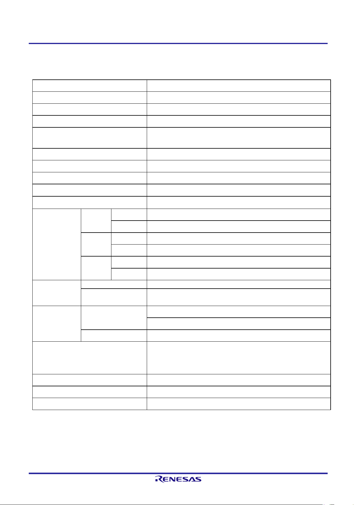
1. Overview
1.1 Purpose
The board of Renesas Solution Starter Kit for RX23E-A (called “RSSKRX23E-A board” or “the board” below)
is an evaluation tool for the Renesas microcontroller RX23E-A. This manual describes the hardware aspect of
the RSSKRX23E-A board in detail. The manual also describes how to connect the board to a PC and sensors
for evaluation.
1.2 Mounted MCU
Table 1-1 lists the specifications of the MCU mounted on the board. The RX23E-A MCU mounted on the
board contains two low-noise 24-bit ∆-Σ A/D converters (DSADs). A DSAD contains a programmable gain
instrumentation amplifier (PGA). The gain can be selected from x1, x2, x4, x8, x16, x32, x64, and x128. It also
contains an analog front-end (AFE) circuit suitable for measuring sensors such as a thermocouple, RTD, and
strain gage. Up to 6 channels of measurement can be performed by switching the analog multiplexer (AMUX)
in the AFE.
For details on the MCU operating conditions, and DSAD and AFE settings, refer to “RX23E-A Group User's
Manual: Hardware”.
Table 1-1 Mounted MCU
Product group RX23E-A
Maximum CPU operating frequency 32 MHz
Package/number of pins LFQFP/48
RAM 32 KB
Storage temperature range -55 to +125°C
R20UT4542EJ0110 Rev.1.10 Page 1 of 39
Mar.30.20
Page 14

RSSKRX23E-A 1. Overview
1.3 Functions and Features
The board has the following functions and features.
(1) Functions and features for hardware and system design engineers
• A/D converter evaluation circuit
• Thermocouple measurement circuit
• Resistance temperature detector (RTD) measurement circuit
• Strain gage measurement circuit
• Power supply selection circuit
• FW controlling DSAD and AFE operation
• Transmission of measurement results and reception of AFE settings using USB communication
(2) Functions and features for software design engineers
• RX23E-A programming and debugging
• Switches, LEDs, and other user interfaces
The board has all circuits required for microcontroller operation.
R20UT4542EJ0110 Rev.1.10 Page 2 of 39
Mar.30.20
Page 15
RSSKRX23E-A 1. Overview
1.4 Specifications
Table 1-2 Specifications of the RSSKRX23E-A Board
Item Specification
Board model name RTK0ESXB10C00001BJ
MCU input clock 8-MHz external crystal oscillator
Applicable emulator E1, E2, and E2 Lite
Power input terminal block
Signal input terminal block CN2: Signal input terminal block (13-pin)
Analog power output terminal block CN1: Analog power output terminal block (2-pin)
Thermocouple connector CN3: Miniature thermocouple socket (2-pin) Material: copper-copper
Emulator connector CN7: 14-pin interface connector
On-board RTD Pt100 Class F0.3 (Class B) Model: PTS060301B100RP100
Connector CN6: USB serial communication connector USB mini-B
Driver U3: FT232RL
Connector J6: Pin header (3-pin 2.54mm pitch)
Driver U5: R2A25416SP
Connector J7: Pin header (3-pin 2.54mm pitch)
Driver ISL3159EFUZ
Communication
interfaces
On-board LDO
USB
CAN
RS-485
Model ISL80410IBEZ
Device specifications
CN4: System power input terminal block (2-pin)
CN5: Analog power input terminal block (2-pin)
Operating voltage range: 6 to 40 V (Note)
Output setting: 5 V (2.5 to 12 V variable output)
User interfaces
LEDs
Switches SW1: User switch SW2: External MCU reset switch
Universal through-holes
Board outline 120mm x 92mm
Operating temperature Room temperature
Operating humidity No condensation allowed
Note When the on-board LDO is used, the operating voltage range of this product is 6.5 to 12 V due to limitations of
peripheral components.
LED2: Power LED (VCC) Color: Green
LED1: User LED (PH2) Color: Red
2.54-mm pitch
J1: 4-pin through holes
J2: 12-pin through holes
J3, J4: 10-pin through holes
R20UT4542EJ0110 Rev.1.10 Page 3 of 39
Mar.30.20
Page 16
RSSKRX23E-A 1. Overview
RX23E-A
USB
mini B
Terminal
Bloc ks
USB
Se ri al
Conv erter
Crystal
Oscill ator
RX23E-A RSSK
The rmo coupl e
Connector
Em ula tor
Con nect or
User ’s
Swi tch
RESET
Swi tch
Passive
Filters
and
Sens or
Selection
Circuit s
Analog Plane Dig ital P la ne
Terminal
Bloc ks
User ’s
LED
Terminal
Bloc ks
Pin
Head ers
USB S erial
Comm unica tion
Analo g Power
Suppl y
Va
5V
LDO
AVCC0
VCC
CAN
Driv er
VLD O
Vd Vbus
UART Commun ication
Terminal
Bloc ks
VCC
E1, E2, E2 Lite
RS-485
Driv er
CAN C ommun icatio n
JP1 4
TXD1 R XD1 #RTS 1
Th ro ugh
Hole s
Th ro ugh
Hole s
Powe r
LED
MD/FI NED #RE S
Si gnals
Pin
Head ers
TXD1 RXD1
CTXD0 CRXD0
CTXD CRXD
Terminal
AV SS0
AVCC0
LSW
Analo g
Si gnals
Analo g
Si gnals
Analo g
Si gnals
Exciting Voltage
Out put
Sens ors
Ther moco uple
Vd
Sy st e m Po w er
Suppl y
Vbus
JP1 5
RS-485
Comm unica tion
Shiel d wire
Analo g Signal
Refe rence Voltage
AVCC0
Va
Univ ersa l
Th ro ugh
Hole s
CN1
CN2
CN3
CN5 CN4
U2
J1
J5
TH1
U1
Y1
J2, J3, J4
SW1
SW2
CN7
U4
U5
U3
J6
J7
CN6
1.5 System Block Diagram
Figure 1-1 RSSKRX23E-A Board System Block Diagram
R20UT4542EJ0110 Rev.1.10 Page 4 of 39
Mar.30.20
Page 17
RSSKRX23E-A 1. Overview
1.6 Overview and Layout
Figure 1-2 Overview of the RSSKRX23E-A Board (Front Side)
Figure 1-3 Overview of the RSSKRX23E-A Board (Back Side)
R20UT4542EJ0110 Rev.1.10 Page 5 of 39
Mar.30.20
Page 18
RSSKRX23E-A 2. Using the RSSKRX23E-A Board
When analog and digital power
CN2
CN2
2. Using the RSSKRX23E-A Board
2.1 Operating Conditions
Table 2-1 lists the recommended operating conditions of the board.
Observe the recommended operating conditions when using the board. The use of the board without
observing any recommended operating condition may cause unpredictable operation. The use of the
board without observing any maximum rating may cause a failure or damage to the board.
Table 2-1 Recommended Operating Conditions
Condition: VSS = AVSS0 = 0 V
Recommended
Item Symbol Input pin
Vd
System
power
supply
Analog
power
supply
Digital pin VIN See Section 4.5. -0.3 to VCC + 0.3 Absolute maximum rating
Analog pin V
LSW pin I
Note 1. Operation of USB serial communication, CAN communication, and RS-485 communication are guaranteed
Note 2. Although the operating voltage of the LDO (ISL80410) is 6 to 40 V, the recommended LDO operating range
Note 3. Supply the power to VCC and AVCC0 simultaneously or sequentially in this order.
Note 4. The R0N pin is connected to the LSW pin when pins 3 and 4 of JP7 are connected.
Note 5. When pins 1 and 2 are connected, Vd is directly connected to VCC.
(VCC)
CN4
Vd
AVCC0 CN5
AIN
LSW
only in condition of inside recommended operating range (4.5~5.25V). RX23E-A can operate at 1.8 to 5.5 V.
on the board is 6.5 to 12 V, considering the capacitor rated voltage, power line voltage drop, and heat
generation of the LDO.
When pins 5 and 6 are connected, VBUS (USB power supply) is connected to VCC.
(R0P, R0N, 0~9)
CN3
(AN10, AN11)
(LSW, R0N (Note 4))
operating
range
4.5 to 5.25 V
(Note 1)
6.5 to 12 V
(Note 2)
2.7 to 5.5 V
(Note 3)
-0.3 to AVCC0 + 0.3 Absolute maximum rating
- 30 mA When the LSW is switched ON
Maximum
rating
6.0 V
20 V
6.5 V
Condition
When the LDO is not used
(when pins 1-2 or 5-6 of JP14
are connected) (Note 5)
When the LDO is used (when
pins 5-6 of JP14 are connected)
supplies are separated (when
pins 1-2 of JP14 are connected)
and VCC > 2.7 V
R20UT4542EJ0110 Rev.1.10 Page 6 of 39
Mar.30.20
Page 19

RSSKRX23E-A 2. Using the RSSKRX23E-A Board
Analog power
Separate analog/digital
Pins 2-3
USB operation for
Pins 1-2
Do not supply the
Vd
RX23E-A
Vbus
LDO
Va
Vd
VLD O
JP1 4
JP1 5
Sy st e m P o we r
Select Jumper
Analo g P ower
Select Jumper
Sy ste m Po wer Supply
USB B us Power
Analo g P ower Supp ly
VCC
E2 Lite
Emula tor Power Su pply
AVCC0
241
6
5
3
Vbus
1
2
3
CN7
CN8
CN4
CN5
2.2 Selecting Power Supplies
Figure 2-1 shows the power supply configuration of the board. Table 2-2 shows how to select each power
supply on the board. Before using a combination of power supplies not listed in Table 2-2, carefully check the
recommended operating conditions in Table 2-1.
Figure 2-1 Power Supply Configuration of the RSSKRX23E-A Board
Table 2-2 Power Selection Methods
Input power
supply
Vd
Vbus Vbus Vbus Pins 5-6
Emulator
Note 1. When connecting pins 2 and 3 of JP15, do NOT supply the power to Va. If the power is supplied to Va,
VCC and AVCC0 are connected on the board, resulting in a short-circuit between Va and VCC.
Note 2. The emulator power supply is connected to VCC. If pins 3 and 4 of JP14 are left connected and the power
is supplied from the emulator, voltage is applied to the output of U2 and U2 may be damaged. Never
supply the power from the emulator when the pins are connected.
Digital power
supply VCC
supply
AVCC0
JP14
connection
Vd Vd Pins 1-2
Vd Va Pins 1-2 Pins 1-2
VLDO VLDO Pins 3-4
Emulator Emulator
Emulator Va
Pins 1-2
(Note 2)
(Note 2)
JP15
connection
Pins 2-3
(Note 1)
Pins 2-3
(Note 1)
(Note 1)
Pins 2-3
(Note 1)
Pins 1-2
Remarks
Initial default setting
power supplies
simple check
Do not supply the
power to Vd or Vbus.
power to Vd or Vbus.
R20UT4542EJ0110 Rev.1.10 Page 7 of 39
Mar.30.20
Page 20

RSSKRX23E-A 2. Using the RSSKRX23E-A Board
When pins 1-2 are connected
When pins 2-3 are connected
USB serial
RSSKRX23E-A EVB
RX23E
USB-
mulator
Connector
USB 2.0FS
2.3 Connecting a PC to the Board
Figure 2-2 shows a configuration used when a PC is connected to the board. Table 2-3 lists functions
available when a PC is connected to the board.
When connecting a PC to the board, supply the power to the board as described in "2.2 Selecting Power
Supplies".
The board can be connected to the Renesas on-chip debugging emulator (E1, E2, E2 Lite) to debug user
code. When using the emulator, connect the 14-pin interface cable attached with the emulator to CN7. Before
supplying the power from the emulator, check that the following conditions are satisfied. If any of the
conditions is not satisfied, a failure may occur in the board, power supply, and/or emulator.
• The power is NOT supplied to VCC.
• Pins 3 and 4 of JP14 are NOT connected.
3.3-V power is supplied from E2 Lite. Note that USB serial communication, RS-485 communication, and CAN
communication do not operate. When using the emulator, refer to the user's manual of the emulator.
The board contains a USB serial conversion IC. SCI1 interface of the MCU and USB serial conversion IC are
connected and communication with a PC is available by USB serial communication. To use USB serial
communication, connect a USB cable to CN6 (USB mini-B connector).
For details on PC Tool Programs, refer to the “RSSKRX23E-A PC Tool Program Operation Manual”.
For details on the circuits around CN6 and CN7, see “3.1 USB Serial Communication Circuit” and “3.2
Emulator Peripheral Circuit”.
UART
COM
-A
I/F
Figure 2-2 Connecting a PC
Table 2-3 Functions Available When a PC Is Connected
Item Connected to
Emulator CN7 Disabled
communication
CN6 FW write via the SCI interface Communication with PC Tool Program
mini-B
USB
E
Emulator
JP17 connection and function
Code debugging
FW write via the FINE interface
PC Tool
Program
R20UT4542EJ0110 Rev.1.10 Page 8 of 39
Mar.30.20
Page 21

RSSKRX23E-A 2. Using the RSSKRX23E-A Board
2.4 Using the Analog Input Circuit
2.4.1 Overview of the Analog Input Circuit
The analog input circuit on the board has the following functions.
• DSAD measurement circuit
• Thermocouple measurement circuit
• Reference junction compensation circuit using the on-board RTD
• Four-wire RTD measurement circuit
• Three-wire RTD measurement circuit
• Strain gage measurement circuit
This manual covers the circuit configuration required for implementing each function and the relationship
between the DSAD measurement result and input signal in two’s complement format. For details on
processing for converting the DSAD measurement result to a physical quantity, refer to the application notes
related to sensor measurement.
To switch the function, it is necessary to change the jumper pin connection and DSAD and AFE settings. The
jumper pin connection and built-in FW are factory-set for the DSAD measurement circuit using AIN3 and AIN2
or AIN9 and AIN8.
Table 2-4 lists each function of the analog input circuit and corresponding jumper pin connection. Table 2-5
lists factory settings of the DSAD and AFE.
R20UT4542EJ0110 Rev.1.10 Page 9 of 39
Mar.30.20
Page 22

RSSKRX23E-A 2. Using the RSSKRX23E-A Board
Connection
X X X X X X AIN3
AIN2
N/A
Thermocouple
Three-wire
AIN4(REF1N)
Strain gage
976.563
976.563
Table 2-4 Functions of the Analog Input Circuit and Corresponding Jumper Settings
Jumper pin connection Used pins of the MCU (pin function)
Function
Factory
settings
DSAD
measurement
circuit
JP7 JP8 JP9 JP10 JP11 JP12
5-6 5-6 1-2
1-2 and
X X X X
3-4
1-2 and
3-4
1-2 and
3-4
1-2 N/A N/A N/A
1-2 AIN9 AIN8 N/A
Positive
side
input
Negative
side
input
Others
measurement
X X X X X X AIN11 AIN10 N/A
circuit
Reference
junction
compensation
X X 2-3
5-6 and
7-8
1-2 and
3-4
2-3 AIN7 AIN6
circuit
RTD
measurement
X X 1-2
1-2 and
3-4
5-6 and
7-8
1-2 AIN7 AIN6
circuit
Four-wire RTD
measurement
circuit
measurement
circuit
X X 1-2
3-4 or
5-6
5-6 X X X X AIN1 AIN0
1-2 and
3-4
1-2 and
3-4
1-2 AIN7 AIN6
X: Don't care N/A: Not applicable
Note The thermocouple measurement circuit is independent of the JP7 to JP12 jumper pin connection.
Table 2-5 Factory Settings of the DSAD and AFE
Setting value
Item Symbol
Polarity DSAD0 DSAD1
Remarks
AIN4(REF1N)
AIN5(REF0N)
AIN9(IEXC)
AIN5(REF1P)
AIN8(IEXC)
AIN9(IEXC)
AIN4(REF1N)
AIN5(REF1P)
AIN9(IEXC)
REF0N,
REF0P
Note The bias voltage generator and excitation current source are not used in the factory setting.
R20UT4542EJ0110 Rev.1.10 Page 10 of 39
Mar.30.20
Measurement pin ―
Positive AIN3 AIN9
Negative AIN2 AIN8
Positive REFOUT REFOUT
Reference voltage VREF
Negative AVSS0 AVSS0
Gain GAIN ― 1x 1x
Data rate DR ―
SPS
SPS
Directly connected to the DSAD
(Both the PGA and buffer amplifier are
bypassed)
Internal reference voltage used.
REFOUT: 2.5 Vtyp.
Oversampling ratio: 512
Page 23

RSSKRX23E-A 2. Using the RSSKRX23E-A Board
AIN 2 (Lo)
U1
RX23 E-A
AIN 8 (Lo)
AIN9 (Hi)
AIN3 (Hi)
Volt age
Measurement
8
9
2
3
AIN
R10 (0Ω)
41
42
C23
C12
NM
NM
NM
R11 (0Ω)
C11
R17 (0Ω)
47
48
C26
C18
NM
NM
NM
R18 (0Ω)
C17
Commo n mode I np ut
123
4
567
8
1 2 3
JP1 2
JP1 1
Signal Inp ut
Signal Inp ut
Volt age
Measurement
CN2
RSSKRX23E-A
2.4.2 DSAD Measurement Circuit
Figure 2-3 shows an example usage of the DSAD measurement circuit on the board.
Figure 2-3 Example Usage of DSAD Measurement Circuit
The FW built onto the board at shipment is set to measure the differential voltage between AIN3 and AIN2 and
that between AIN9 and AIN8 using two channels DSAD0 and DSAD1 in the MCU. The input voltage between
pins 3 and 2 of CN2 (between AIN3 and AIN2) and between pins 9 and 8 of CN2 (between AIN9 and AIN8)
are being used for the measurement. The differential input voltage VID can be obtained from the DSAD
measurement result ADDATA using the following expression.
Before applying voltage to the DSAD measurement circuit, check the following conditions. If either condition is
not satisfied, measurement cannot be performed correctly.
The absolute input voltage range and differential voltage input range depend on the DSAD settings. For
details, refer to "RX23E-A Group User's Manual: Hardware".
During evaluation with the DSAD measurement circuit, self-noise of the DSAD and PGA can be measured by
short-circuiting input pins using JP2 and JP5. To short-circuit input pins, fix the input pin potential to satisfy
condition (1). The PGA input bias current may cause the input pin potential to be outside the absolute input
voltage range. Sample methods for fixing the input pin potential are listed below.
When using method (a) or (b) for measurement, check that the applied voltage is within the range of condition
(1). Depending on connection, the differential input impedance becomes imbalanced, and the circuit may be
susceptible to common mode noise.
R20UT4542EJ0110 Rev.1.10 Page 11 of 39
Mar.30.20
=
× 2
×
[V]
2
(1) The voltage between each AIN and AVSS0 is within the absolute input voltage range for DASD
measurement.
(2) The voltage between AIN pins is within the differential voltage input range.
(a) Connect an external stable potential to one measurement pin.
(b) Connect one measurement pin to GND via a resistor.
(c) Apply bias voltage to one measurement pin using the AFE bias voltage generator.
Page 24

RSSKRX23E-A 2. Using the RSSKRX23E-A Board
1
Thermocoupl e
2
AIN11 (Hi)
AIN 1 0 (Lo )
CN3
1
2
AIN 1 0 (Lo )
AIN11 (Hi)
R19
R20
C27
C20
C19
Thermocoupl e
Measurement
U1
RX23 E-A
RSSKRX23E-A
2.4.3 Thermocouple Measurement Circuit
Figure 2-4 shows the thermocouple measurement circuit on the board.
Figure 2-4 Thermocouple Measurement Circuit
CN3 is a connector socket on board the RSSKRX23E-A (material : copper-copper) used for the thermocouple
input pins. Thermocouple attached with the board can be connected to CN3 for measurement.
Connect the positive side of the thermocouple to AIN11 pin of CN3 and the negative side to AIN10 pin. The
output from the thermocouple (thermoelectromotive force) is input to AIN11 and AIN10 and the differential
voltage between AIN11 and AIN10 is measured with the DSAD. The thermoelectromotive force V
obtained from the DSAD measurement result AD
using the following expression.
DATA
× 2
=
×
[]
2
For thermocouple measurement, fix the input pin potential. The PGA input bias current may cause the input
pin potential to be outside the absolute input voltage range.
Measuring a temperature with the thermocouple requires cold junction compensation or reference junction
compensation. The board enables reference junction compensation using the on-board RTD. For details on
the reference junction compensation circuit using the on-board RTD, see 2.4.4 “Reference Junction
Compensation Circuit Using the On-Board RTD”
TEMP
can be
R20UT4542EJ0110 Rev.1.10 Page 12 of 39
Mar.30.20
Page 25

RSSKRX23E-A 2. Using the RSSKRX23E-A Board
R13
R14
C14
C13
Refe rence
Resistor
1
Ther moco upl e
2
AIN11 (Hi)
AIN 10 (L o)
REF1N(AIN4)
U1
RX23 E-A
CN3
1
2
AIN 10 (L o)
AIN11 (Hi)
IEXC0 (AIN9)
AIN8 (Unused)
R17 (0Ω)
47
48
C26
C18
NM
NM
R19
R20
C27
C20
C19
NM
R18 (0Ω)
AIN 6 (Lo)
45
46
C25
RTD1
pt10 0
5.1kΩ
R12
390Ω
I
EXC0
Refe rence Buffer
Head room Res ist or
AIN7 (Hi)
REF 1P(A IN5)
R15
R16
C16
C15
C24
RTD
Measurement
Exci tation
Curr ent
Out put
Ther moco upl e
Measurement
Ext ernal
Refe rence
Inpu t
43
44
8
9
6
7
4
5
1
2
3
123
4
5
678
123
4
567
8
1 2 3
R4
JP9
JP1 0
SO10
JP1 2
CN2
0.1% 15pp m
C17
AIN
JP1 1
RSSKRX23E-A
2.4.4 Reference Junction Compensation Circuit Using the On-Board RTD
Figure 2-5 shows the reference junction compensation circuit on the board.
On the board, the temperature near CN3 is detected with the on-chip resistance temperature detector, RTD1,
for reference junction compensation for thermocouple measurement. For RTD1 measurement, a four-wire
ratiometric measurement method is used. The excitation current I
in the path shown by the arrow. The voltages at both ends of RTD1 are input to AIN7 and AIN6 and they are
measured with the DSAD. The voltages at both ends of the reference resistor R4 are input to REF1P (AIN5)
and REF1N (AIN4) and used as DSAD external reference voltages. The RTD1 resistance can be indicated
using the DSAD measurement result AD
× 1 =
When I
is deleted from both sides,
EXC0
Figure 2-5 Reference Junction Compensation Circuit
× × 2
×
as shown below.
DATA
[]
2
EXC0
is output from AIN9 and is made to flow
×
2
[]
EXC0
1 =
With the above expression, the RTD1 resistance can be obtained independently of the excitation current I
Use a built-in reference buffer (RBUF) with AFE for external reference inputs REF1N and REF1P. The use of
the RBUF can reduce the current input to the external reference input pin. Note that the use of the RBUF
narrows the absolute input voltage range for external reference. R12 is provided to make the voltages at both
ends of R4 fall within the absolute input voltage range for external reference when the RBUF is used.
× 2
R20UT4542EJ0110 Rev.1.10 Page 13 of 39
Mar.30.20
.
Page 26

RSSKRX23E-A 2. Using the RSSKRX23E-A Board
R13
R14
C14
C13
Refe re nce
Resistor
REF1N(AIN4)
U1
RX23 E-A
IEXC0 (AIN9 )
AIN8 (Unused)
R17 (0Ω)
47
48
C26
C18
NM
NM
NM
R18 (0Ω)
AIN 6 (L o)
45
46
C25
5.1kΩ
R12
390Ω
IEXC0
AIN7 (Hi)
REF 1P(AIN5)
R15
R16
C16
C15
C24
RTD
Measure ment
Exci tation
Curr en t
Out put
Ext ernal
Refe re nce
Inpu t
43
44
8
9
6
7
4
5
1
2
3
123
4
5
678
123
4
567
8
1 2 3
R4
JP9
JP1 0
JP1 1
JP1 2
CN2
0.1% 15ppm
C17
4-wire
RTD
-
+
AIN
SO10
RSSKRX23E
-A
Refe re nce Buff er
Headroom Res istor
2.4.5 Four-Wire RTD Measurement Circuit
Figure 2-6 shows the four-wire RTD measurement circuit on the board.
Figure 2-6 Four-Wire RTD Measurement Circuit
A configuration similar to that for on-board RTD measurement is used for four-wire RTD measurement.
Connect two pins of same polarity of a four-wire RTD to pins 9 (AIN9) and 7 (AIN7) of CN2 and two pins of the
other polarity to pins 6 (AIN6) and 5 (AIN5) of CN2. The excitation current I
made to flow in the path shown by the arrow. The voltages at both ends of the RTD are input to AIN7 and
AIN6 as detection signals and they are measured with the DSAD. The voltages at both ends of the reference
resistor R4 are input to REF1P (AIN5) and REF1N (AIN4) and used as DSAD external reference voltages.
The RTD resistance RTD
×
When I
is deleted from both sides,
EXC0
With the above expression, the RTD resistance RTD
current I
EXC0
.
In the same way as for on-board RTD measurement, RBUF is used for external reference input.
R20UT4542EJ0110 Rev.1.10 Page 14 of 39
Mar.30.20
× 2
=
can be indicated using the DSAD measurement result AD
4-wire
× × 2
=
×
2
×
[]
2
[]
can be obtained independently of the excitation
4-wire
is output from AIN9 and is
EXC0
as shown below.
DATA
Page 27

RSSKRX23E-A 2. Using the RSSKRX23E-A Board
R13
R14
C14
C13
Refe re nce
Resistor
REF1N(AIN4)
U1
RX23 E-A
IEXC0 (AIN9)
IEXC1
(AIN8)
R17 (0Ω)
47
48
C26
C18
NM
NM
NM
R18 (0Ω)
AIN 6 (L o)
45
46
C25
5.1kΩ
R12
390Ω
IEXC0
AIN7 (Hi)
REF 1P(AIN5)
R15
R16
C16
C15
C24
RTD
Measurement
Exci tation
Curr en t
Out put
Ext ernal
Refe re nce
Inpu t
43
44
8
9
6
7
4
5
1
2
3
123
4
5
678
1
234
567
8
1 2 3
R4
JP9
JP1 0
JP1 1
JP1 2
CN2
0.1% 15ppm
C17
3-wire
RTD
-
+
AIN
IEXC1
RSSKRX23E
-A
Refe re nce Buff er
Headroom Res istor
2.4.6 Three-Wire RTD Measurement Circuit
Figure 2-7 shows the three-wire RTD measurement circuit on the board.
Figure 2-7 Three-Wire RTD Measurement Circuit
Connect one pin at one side of a three-wire RTD to pin 7 (AIN7) of CN2 and two pins of the other polarity to
pins 6 (AIN6) and 5 (AIN5) of CN2. The excitation currents I
are made to flow in the path shown by the arrow. The voltages at both ends of the RTD are input to AIN7 and
AIN6 as detection signals and they are measured with the DSAD. The voltages at both ends of the reference
×
resistor R4 are input to REF1P (AIN5) and REF1N (AIN4) and used as DSAD external reference voltages.
The RTD resistance RTD
When
With the above expression, when the excitation currents I
RTD
can be obtained independently of the excitation currents.
3-wire
× 4
=
+
) × × 2
+
[]
is indicated using the DSAD measurement result AD
3-wire
(
=
=
×
,
2
×
= 2 ×
2
. When I
[]
EXC0
EXC1
and I
and I
EXC0
are output from AIN8 and AIN9 and
EXC0
DATA
is deleted from both sides,
are equal, the RTD resistance
EXC1
as shown below.
In the same way as for on-board RTD and four-wire RTD measurement, RBUF is used for external reference
input.
R20UT4542EJ0110 Rev.1.10 Page 15 of 39
Mar.30.20
Page 28

RSSKRX23E-A 2. Using the RSSKRX23E-A Board
CN2
C21
C8
C7
R6(0 Ω)
R7(0
Ω)
REF 0N
U1
RX23 E-A
AIN 0 (L o)
39
40
C22
AIN1 (Hi)
REF 0P
R8
R9
C10
C9
Strain Gauge
Measure ment
Ext ernal
Refe rence
37
38
0
1
R0N
R0P
1
3
5
JP7
AVCC0
36
LSW
LSW Low S ide Switch
2 4 6
JP8
2 4 6
1
3
5
EXC Lo
Str ain
Gauge
1-Gauge 4
-Wir e
AIN
EXC Hi
Si g na l Lo
Si g nal Hi
TH1
Shielded Wire
RSSKRX23E-A
2.4.7 Strain Gage Measurement Circuit
Figure 2-8 shows the measurement circuit for a strain gage (four-wire, single-gage method) on the board.
Figure 2-8 Strain Gage (Four-wire, Single-gage Method) Measurement Circuit
For the board, as an example of strain gage measurement, a measurement circuit for the four-wire, single-
gage method using a Wheatstone bridge is used.
Connect a strain gage that configured a bridge circuit to R0N pin (REF0N), R0P pin (REF0P), pin 0 (AIN0),
and pin 1 (AIN1) of CN2. Use AVCC0 and AVSS0 as excitation voltage sources to drive the bridge circuit. The
voltages of the output pins of the strain gage are input to AIN0 and AIN1 and the differential voltage is
measured with the DSAD. AVCC0 and AVSS0 are used as external reference inputs. When the strain gage
has a shielded wire, it can be connected to TH1 or the negative pin of CN1.
As an external reference input, LSW can be connect instead of AVSS0. The LSW pin is connected to AVSS0
via an analog switch in the MCU. This switch can be changed according to the MCU register setting. Power
supply to the strain gauge can be supplied by turning on the switch, and power supply to the strain gauge can
be stopped by turning off the switch. Supplying the power to the strain gage only during measurement can
reduce power consumption. The allowable current to the LSW pin is 30 mA. When using the LSW pin,
consider the allowable current.
If the LDO is used as the power supply for strain gage measurement (by connecting pins 3 and 4 of JP14), be
careful about the LDO output current. The maximum output current of the LDO mounted on the board,
ISL80410, is 150 mA. If current exceeding the maximum output current is required, do not use the
LDO.
R20UT4542EJ0110 Rev.1.10 Page 16 of 39
Mar.30.20
Page 29

RSSKRX23E-A 2. Using the RSSKRX23E-A Board
In this circuit, the relationship between the differential voltage between AIN0 and AIN1 V
can be indicated using the gage coefficient K (strain gage sensitivity) as shown below.
1
=
× × ×(0 0)[V]
4
The differential voltage V
can be indicated using the DSAD measurement result AD
strain
expression.
2 × (0 0)
=
×
2
When V
, AVCC0, and AVSS0 are deleted from the above two expressions, the strain ratio ε can be
strain
indicated with the following expression.
=
2 × 4
×
×
2
and strain ratio ε
strain
with the following
DATA
R20UT4542EJ0110 Rev.1.10 Page 17 of 39
Mar.30.20
Page 30
RSSKRX23E-A 2. Using the RSSKRX23E-A Board
Pin name
Handling result
Handling method
REF0N
Connected to AVSS0 directly or via a resistor.
Connect pins 5-6 of JP7.
LSW
Connected to AVSS0 directly or via a resistor.
2.4.8 Handling Unused Pins in the Analog Input Circuit
If there is an unused pin in the analog input circuit, handling the unused pin according to Table 2-6 is
recommended. If the unused pin is not handled accordingly, the circuit becomes susceptible to external noise
and static electricity, which may deteriorate performance and cause a failure.
Table 2-6 Handling Unused Pins in the Analog Input Circuit
REF0P Connected to AVCC0 directly or via a resistor. Connect pins 5-6 of JP8.
AIN0 to AIN11 Connected to AVSS0 directly or via a resistor.
Use a soldering side short pad (SO1-SO13) to
connect the pin to AVSS0.
R20UT4542EJ0110 Rev.1.10 Page 18 of 39
Mar.30.20
Page 31

RSSKRX23E-A 3. Microcontroller Peripheral Circuits
VSS
U1
RX23E-A
TXD
D4
14
16
VCC
R47
VCC
13
R60
R69
R64
R61
R65
RXD
RTS#
3
1
5
CTS #
CN6
USB mi ni-B
Vbus
(To JP14)
VSS
VBUS
GN D
USBDM
USBDP
NC
VSS
VCC IO
VCC
USBDM
U3
FT232RL
USBDP
R68
Zdiff = 90Ω±15%
USB2.0 Differential Impedance
11
4
20
C55C54
L1
C52
16
15
1
2
3
4
5
C51
USB-Serial C onverter
3. Microcontroller Peripheral Circuits
3.1 USB Serial Communication Circuit
Figure 3-1 shows the USB serial communication circuit on this board.
Figure 3-1 USB Serial Communication Circuit
The board has a USB serial communication conversion IC (U3: FT232RL). The FT232RL operating voltage
range is 4.0 to 5.25 V. To use USB serial communication, make the following settings.
• Apply 4.0 to 5.25 V to VCC.
• Connect pins 2 and 3 of JP17.
(For details on the JP17 circuit configuration, see “3.2 Emulator Peripheral Circuit”.)
R20UT4542EJ0110 Rev.1.10 Page 19 of 39
Mar.30.20
Page 32

RSSKRX23E-A 3. Microcontroller Peripheral Circuits
Boot mode
Writes the FW using the SCI
Allows you to write the FW using
VCC
VSS
RESET(SW2)
CN7
U1
RX23E-A
1
3
5
7
9
11
13
2
4
6
8
10
12
14
R78
R79
11
5
C60
VSS
VSS
VSS
R81
JP17
1
2
3
R82
R83
R84
C58
Emulator
USB
Programmer
Selector
VCC
VCC
3.2 Emulator Peripheral Circuit
Figure 3-2 shows the emulator peripheral circuit on the board. Table 3-1 lists the JP17 connections and
corresponding functions.
Figure 3-2 Emulator Peripheral Circuit
Table 3-1 JP17 Connections and Corresponding Functions
JP17
connection
Pins 1-2
Pins 2-3 Single-chip mode
Operating mode Function Remarks
(SCI interface)
interface.
Debugs and writes the FW using
the emulator.
USB serial communication (CN6).
Applicable emulator:
E1, E2, and E2 Lite
When using the emulator, connect it to CN7. Before supplying the power from the emulator, carefully
check that the power does not collide with the input power supply or LDO output.
By pressing the RESET button (SW2) MCU RES# pin can be reset.
The MCU operating mode can be selected from the boot mode (SCI interface) or single-chip mode by
changing the JP17 setting. During power on, never change the JP17 setting. The MCU may perform
unpredictable operation.
For details on the reset operation, and boot mode operation and functions, refer to “RX23E-A Group User's
Manual: Hardware”.
For details on how to use the emulator, refer to the user's manual of the emulator.
R20UT4542EJ0110 Rev.1.10 Page 20 of 39
Mar.30.20
Page 33

RSSKRX23E-A 3. Microcontroller Peripheral Circuits
VCC
21
VSS
120Ω
R57
U1
RX23E-A
U5
J6
1
2
3
CAN Transceiver
S
TXD
VCC
RXD
GN D
CAN_ L
CAN_ H
R77
OPEN
1
Ter mination
JP16
VSS
20
19
R43
R44
R42
3
8
1
4
2
7
6
C57
CAN_ H
VSS
CAN_ L
NM
2
3
REF
VSS
5
C62
24
R94
U1
RX23E-A
U4
ISL3159EF
J7
1
2
RS-485 Driver
RO
DI
DE
RE#
GN D
VSS
23
28
R40
R35
1
4
3
2
6
7
VSS
A/Y
B/Z
A/Y
VCC
R93
R92
VSS
5
NM
8
VSS
B/Z
3
C61
VSS
R96 390Ω
R97
220Ω
D5
VCC
VCC
VCC
VSS
R95 390Ω
3.3 RS-485 Communication Circuit
Figure 3-3 shows the RS-485 communication circuit on the board.
The RS-485 communication circuit on the board has a PROFIBUS DP-compliant, half-duplex communication
RS-485 driver ISL3159EFUZ. A 220-Ω termination resistor and a 390-Ω failsafe bias resistor are mounted on
R95, R96, and R97.
Figure 3-3 RS-485 Communication Circuit
3.4 CAN Communication Circuit
Figure 3-4 shows the CAN communication circuit on the board.
Figure 3-4 CAN Communication Circuit
The CAN communication circuit on the board has a CAN transceiver. The CAN bus can be connected directly
from J6. As a termination resistor, a 120-Ω resistor is connected between CAN-H and CAN-L. When the
termination resistor is required, connect pins 2 and 3 of JP16. When it is not required, connect pins 1 and 2 of
JP16.
R20UT4542EJ0110 Rev.1.10 Page 21 of 39
Mar.30.20
Page 34

RSSKRX23E-A 3. Microcontroller Peripheral Circuits
VCC
LED1
Red
U1
RX23E-A
R51
VSS
R56
LED2
Green
22
VSS
SW1
VCC
U1
RX23E-A
R80
R85
C59
15
VSS
3.5 LED Circuit
Figure 3-5 shows the LED drive circuit on the board.
ON/OFF of LED1 (red) can be controlled by a port of MCU (PH2). LED2 (green) is a VCC power indicator.
Figure 3-5 LED Drive Circuit
3.6 Switch Input Circuit
Figure 3-6 shows the switch input circuit on the board.
For details on the RESET switch (SW2), see “3.2 Emulator Peripheral Circuit”.
Figure 3-6 Switch Input Circuit
R20UT4542EJ0110 Rev.1.10 Page 22 of 39
Mar.30.20
Page 35

RSSKRX23E-A 3. Microcontroller Peripheral Circuits
VSS
U1
RX23E
-A
C34
C33
6
8
3.7 External Clock Input Circuit
Figure 3-7 shows the external clock input circuit on the board.
The board has an 8-MHz external crystal oscillator as an external clock input source.
Figure 3-7 External Clock Input Circuit
R20UT4542EJ0110 Rev.1.10 Page 23 of 39
Mar.30.20
Page 36

RSSKRX23E-A 4. Board Information
Applicable crimp
Terminal-applicable
4. Board Information
4.1 Using Terminal Blocks
Table 4-1 lists the part used for terminal blocks CN1, CN2, CN4, and CN5, recommended crimp terminal,
crimping tool, and terminal-applicable wire diameter.
Table 4-1 Terminal Blocks and Applicable Crimp Terminal
Part model name
FFKDS/H-2,54
(Note)
Note FFKDSA1/H-5,08 is used as each connector termination.
terminal
AI0.25-8 CRIMPFOX CENTRUS 10S and others AWG 24
Crimping tool
wire diameter
If you want to use an applicable crimp terminal, you can push in the crimp terminal to connect it to a connector
(push-in type). If a crimp terminal or crimping tool is unavailable, you can connect a stripped wire. To use a
stripped wire, follow the procedure below.
i) Push and hold the orange button into the board.
ii) Insert a stripped wire into the pin insertion hole.
iii) Release the orange button slowly.
iv) Lightly pull the wire to confirm that it is fixed.
To remove the crimp terminal and the wire, follow the procedure below.
i) Push and hold the orange button into the board.
ii) Remove the crimp terminal and the wire from the pin insertion hole.
iii) Release the orange button slowly.
R20UT4542EJ0110 Rev.1.10 Page 24 of 39
Mar.30.20
Page 37

RSSKRX23E-A 4. Board Information
Power Output
Terminal block for outputting an analog power supply.
Signal Input
Terminal block for inputting an analog power supply.
USB Serial
Connector for USB serial communication.
Connector for connecting an emulator.
4.2 Connectors
Table 4-2 lists the connectors on the board.
Table 4-2 Connectors
Reference Connector Name Explanation
CN1
CN2
CN3
CN4
CN5
CN6
CN7 Emulator Connector
Terminal Block
Terminal Block
Thermocouple
Connector
System Power Input
Terminal Block
Analog power Input
Terminal Block
Communication
Connector
Use this connector as an excitation voltage source for a strain gage, etc.
Terminal block for inputting analog signals
Miniature thermocouple input socket.
Copper is used for the material of both terminals.
The terminal screws are soldered to the board. Do NOT rotate them.
Terminal block for inputting a system power supply
Use this connector to supply an analog power supply separately from the
system power supply.
The connector type is USB mini-B. Use this connector for communication
with PC Tool Program.
Use the 14-pin interface cable supplied with the emulator.
The applicable emulator is E1, E2, and E2 Lite.
R20UT4542EJ0110 Rev.1.10 Page 25 of 39
Mar.30.20
Page 38

RSSKRX23E-A 4. Board Information
Silk
GND output
Analog GND output for an external device.
Positive reference voltage input pin.
1
AIN1
I/O
Analog signal input pin
3
AIN3
I/O
Analog signal input pin
Analog signal input pin and positive reference voltage input pin.
Analog signal input pin.
Analog signal input pin and excitation current output pin.
Table 4-3 to
Table 4-9 detail each connector.
Table 4-3 CN1: Power Output Terminal Block
printing
+
-
Function I/O Explanation
Power supply
output
(AVCC0)
(AVSS0)
O
O
Analog power supply output for an external device.
Connected to AVCC0.
When using the LDO, carefully observe the current limitation.
Connected to AVSS0.
Table 4-4 CN2: Signal Input Terminal Block
Silk
printing
LSW LSW O LSW output pin
R0N REF0N I/O
R0P REF0P I/O
0 AIN0 I/O Analog signal input pin
2 AIN2 I/O Analog signal input pin
4 AIN4/REF1N I/O Analog signal input pin and negative reference voltage input pin
Connected
MCU pin
I/O Explanation
Negative reference voltage input pin.
Can be connected to the LSW or AVSS0 by changing the JP7 setting.
Can be connected to AVCC0 by changing the JP8 setting.
5 AIN5/REF1P I/O
6 AIN6 I/O
7 AIN7 I/O
8 AIN8/IEXC1 I/O
9 AIN9/IEXC0 I/O
Note The AIN0 to AIN9 pins can be connected to excitation current sources IEXC0 to IEXC3 and used as excitation
current output pins by setting MCU registers.
Can be connected to RTD1 by changing the JP9 setting.
Analog signal input pin.
Can be connected to RTD1 by changing the JP10 setting.
Can be connected to AIN8/IEXC1 by changing the JP11 setting.
Can be connected to RTD1 by changing the JP10 setting.
Can be connected to AIN9/IEXC0 by changing the JP11 setting.
Analog signal input pin and excitation current output pin.
Can be connected to AIN6 by changing the JP11 setting.
Can be connected to AIN7 by changing the JP11 setting.
Can be connected to RTD1 by changing the JP12 setting.
R20UT4542EJ0110 Rev.1.10 Page 26 of 39
Mar.30.20
Page 39

RSSKRX23E-A 4. Board Information
Silk
Connected
AIN11
AIN11
I/O
Analog signal input pin
Silk
GND input
Silk
GND input
Pin No.
Function
I/O
Explanation
2
USBDM
I/O
USB data line D-
NC
Table 4-5 CN3: Thermocouple Connector
printing
AIN10 AIN10 I/O
Note The AIN10 and AIN11 pins can be connected to excitation current sources IEXC0 to IEXC3 and used as excitation
current output pins by setting MCU registers.
MCU pin
I/O Explanation
Analog signal input pin
Table 4-6 CN4: System Power Input Terminal Block
printing
+
-
Function I/O Explanation
Power supply
input (Vd)
(VSS)
I
I GND input. Connected to VSS.
System power supply input. Connected to Vd.
Vd can be connected to VCC by changing the JP14 setting.
Table 4-7 CN5: Analog power Input Terminal Block
printing
+
Function I/O Explanation
Power supply
input (Va)
I
System power supply input. Connected to Va.
Va can be connected to AVCC0 by changing the JP15 setting.
-
(AVSS0)
I GND input. Connected to AVSS0.
Table 4-8 CN6: USB Serial Communication Connector
1 Vbus I
3 USBDP I/O USB data line D+
4
5 GND I GND for an external USB power supply. Connected to VSS.
(Not used)
- -
USB power supply pin. Connected to Vbus.
Vbus can be connected to VCC by changing the JP14 setting.
R20UT4542EJ0110 Rev.1.10 Page 27 of 39
Mar.30.20
Page 40

RSSKRX23E-A 4. Board Information
Pin No.
Function
I/O
Explanation
2
VSS
O
VSS pin
4
(Not used)
-
-
6
(Not used)
-
-
8
VCC
O
VCC pin
10
(Not used)
-
-
12
VSS
O
VSS pin
14
VSS
O
VSS pin
Table 4-9 CN7: Emulator Connector
1 (Not used) - -
3 (Not used) - -
5 (Not used) - -
MD/FINED pin.
7 MD/FINED I/O
9 (Not used) - -
11 (Not used) - -
JP7 can be used to switch between the single-chip mode (pull-up) and
SCI interface boot mode (pull-down).
13 RES# I RES# pin
R20UT4542EJ0110 Rev.1.10 Page 28 of 39
Mar.30.20
Page 41

RSSKRX23E-A 4. Board Information
Pin header for UART communication (not mounted).
Pin header for CAN communication.
Pin No.
Function
I/O
Explanation
1
VCCOUT
O
Power output pin. Connected to VCC.
Pin No.
Function
I/O
Explanation
CAN_H pin.
2
VSS
O
Signal GND connection pin. Connected to VSS.
CAN_L pin.
Pin No.
Function
I/O
Explanation
1
VSS
O
Signal GND connection pin. Connected to VSS.
RS-485 driver non-inverting I/O pin.
4.3 Pin Headers for Communication Interfaces
Table 4-10 lists the pin headers for communication interfaces on the board.
Table 4-10 Pin Headers for Communication Interfaces
Reference Function Explanation
J5
J6
J7
UART
communication
CAN
communication
RS-485
communication
To use this pin header, remove R64 and R66 and mount R62 and R63.
Connected to TXD1 and RXD1 of the MCU.
A CAN transceiver (U5) is mounted.
A 120-Ω termination resistor is mounted between CAN_H and CAN_L.
Can select whether to use of the termination resistor by using JP16
Pin header for RS-485 communication.
An RS-485 driver ISL3159EFUZ (U4) is mounted.
A 220-Ω termination resistor and a 390-Ω failsafe bias resistor are mounted.
Table 4-11 to Table 4-13 detail each communication interface pin header.
Table 4-11 J5: Pin Header for UART Communication (Not Mounted)
RXD input pin.
2 RXIN I
3 TXOUT O
4 VSS O Signal GND connection pin. Connected to VSS.
To use this pin, remove R64 and mount R63.
Connected to RXD1 of the MCU.
TXD output pin.
To use this pin, remove R66 and mount R62.
Connected to TXD1 of the MCU.
Table 4-12 J6: Pin Header for CAN Communication
1 CAN_H I/O
3 CAN_L I/O
Connected to termination resistor R77 by changing the JP16 setting.
Connected to termination resistor R77 by changing the JP16 setting.
Table 4-13 J7: Pin Header for RS-485 Communication
2 B/Z I/O
3 A/Y I/O
RS-485 driver inverting I/O pin.
Connected to the B/Z pin of the driver.
Connected to the A/Y pin of the driver.
R20UT4542EJ0110 Rev.1.10 Page 29 of 39
Mar.30.20
Page 42

RSSKRX23E-A 4. Board Information
Switches the circuit connected to AIN5 to AIN9.
Selecting whether to use the CAN
Can select whether to use the termination resistor
Pins 1-2
-
Select this setting to input an external reference from CN2 to REF0N.
Pins 5-6
REF0N-AVSS0
Connects AVSS0 to REF0N.
4.4 Jumper Pins
Table 4-14 lists the jumper pins on the board.
During power on, do NOT change the setting of any jumper pin. A failure, deterioration, and/or
unpredictable operation may occur.
Table 4-14 Jumper Pins
Reference Function Explanation
JP1 to JP6 Short-circuiting analog inputs Used to short-circuit analog inputs.
JP7 and JP8 Selecting a reference input Used to select REF0N or REF0P input.
JP9 to JP12
JP13 Connecting AIN5/REF1P and AIN6 Can connect AIN5/REF1P and AIN6.
JP14 and JP15 Selecting a power supply
JP16
JP17 Selecting the MCU operating mode
Switching the RTD measurement
circuit
termination resistor
Can select the circuit configuration from external input, onboard RTD measurement, four-wire RTD, or three-wire
RTD measurement.
JP14: Selects Vd, VLDO, or Vbus as VCC.
JP15: Selects Va or VCC as AVCC0.
between CAN_H and CAN_L.
Can select the single-chip mode or boot mode as the
MCU operating mode.
Table 4-15 to Table 4-26 detail each jumper pin.
Table 4-15 JP1 to JP6: Jumper Pins for Short-circuiting Analog Channels
Reference Function Explanation
JP1 Short-circuiting AIN0 and AIN1 Jumper pins for connecting AIN0 and AIN1 (not mounted)
JP2 Short-circuiting AIN2 and AIN3 Jumper pins for connecting AIN2 and AIN3
JP3 Short-circuiting AIN4 and AIN5 Jumper pins for connecting AIN4 and AIN5 (not mounted)
JP4 Short-circuiting AIN6 and AIN7 Jumper pins for connecting AIN6 and AIN7 (not mounted)
JP5 Short-circuiting AIN8 and AIN9 Jumper pins for connecting AIN8 and AIN9
JP6 Short-circuiting AIN10 and AIN11 Jumper pins for connecting AIN10 and AIN11 (not mounted)
Table 4-16 JP7: Jumper Pins for Selecting REF0N Input
JP7
connection
Pins 3-4 REF0N-LSW Connects LSW to REF0N.
Signal name Explanation
R20UT4542EJ0110 Rev.1.10 Page 30 of 39
Mar.30.20
Page 43

RSSKRX23E-A 4. Board Information
JP8
Pins 3-4
-
Not used.
Pins 1-2
-
Select this setting to input signals from CN2 to AIN5/REF1P.
Pins 1-2
Pins 1-2
Pins 1-2
-
Select this setting to input signals from CN2 to AIN9.
Table 4-17 JP8: Jumper Pins for Selecting REF0P Input
connection
Pins 1-2 - Select this setting to input an external reference from CN2 to REF0P.
Pins 5-6 AVCC0-REF0P Connects AVCC0 to REF0P.
Signal name Explanation
Table 4-18 JP9: Jumper Pins for Connecting AIN5/REF1P to the On-Board RTD
JP9
connection
Pins 2-3 RTD1-REF1P
Signal name Explanation
Connects RTD1 to REF1P.
Select this setting to use the on-board RTD.
Table 4-19 JP10: Jumper Pins for Connecting AIN6 and AIN7 to the On-Board RTD
JP10
connection
and
Pins 3-4
Pins 5-6
and
Pins 7-8
Signal name Explanation
- Select this setting to input signals from CN2 to AIN6 and AIN7.
RTD1-AIN6
AIN7-RTD1
Connects AIN6 and AIN7 to both ends of RTD1.
Select this setting to use the on-board RTD.
Table 4-20 JP11: Jumper Pins for Connecting AIN8 and AIN9 to the Three-Wire RTD
JP11
connection
and
Pins 3-4
Pins 5-6
and
Pins 3-4
Signal name Explanation
- Select this setting to input signals from CN2 to AIN6, AIN7, AIN8, and AIN9.
AIN9-AIN7
AIN8-AIN6
Connects AIN6 and AIN8, and AIN7 and AIN9.
Select this setting to connect the three-wire RTD to CN2.
Table 4-21 JP12: Jumper Pins for Connecting AIN9 to the On-Board RTD
JP12
connection
Pins 3-4 RTD1-AIN9
Signal name Explanation
Connects RTD1 to AIN9.
Select this setting to use the on-board RTD.
R20UT4542EJ0110 Rev.1.10 Page 31 of 39
Mar.30.20
Page 44
RSSKRX23E-A 4. Board Information
JP13
Connects VLDO to VCC.
JP15
Connects Va to AVCC0.
JP16
Pins 1-2
-
Disables the termination resistor.
Sets the MCU operating mode to the boot mode (SCI interface).
Table 4-22 JP13: Jumper Pins for Connecting AIN5/REF1P and AIN6
connection
Pins 1-2 AIN5/REF1P-AIN6 Connects AIN5/REF1P and AIN6 (not mounted).
Signal name Explanation
Table 4-23 JP14: Jumper Pins for Selecting a System Power Supply
JP14
connection
Pins 1-2 VCC-Vd
Pins 3-4 VCC-VLDO
Pins 5-6 VCC-Vbus
Signal name Explanation
Connects Vd to VCC.
Select this setting to operate the board with the power supplied from CN4.
Select this setting to operate the board with the LDO output.
Connects Vbus to VCC.
Select this setting to operate the board with the USB power supply.
Table 4-24 JP15: Jumper Pins for Selecting an Analog Power Supply
connection
Pins 1-2 Va-AVCC0
Pins 2-3 AVCC0-VCC
Signal name Explanation
Select this setting to operate the analog side of the MCU with the power
supplied from CN5.
When using this setting, supply power to VCC in advance.
Connects VCC to AVCC0.
Select this setting to use the common power supply for AVCC0 and VCC.
Table 4-25 JP16: Jumper Pins for Selecting Whether to Use the CAN Bus Termination Resistor
connection
Pins 2-3
Signal name Explanation
-
Enables the termination resistor.
Table 4-26 JP17: Jumper Pins for Selecting the MCU Operating Mode
JP17
connection
Pins 1-2 MD/FINED pull-down
Pins 2-3 MD/FINED pull-up
Function Explanation
In the boot mode, the FW written at shipment does not operate.
You can write the FW with USB serial communication (CN6).
Sets the MCU operating mode to the single-chip mode.
Use this setting to operate the FW written at shipment.
You can debug and write the FW using the emulator (CN7).
R20UT4542EJ0110 Rev.1.10 Page 32 of 39
Mar.30.20
Page 45
RSSKRX23E-A 4. Board Information
Communication interface connection through-holes.
Pin No.
Function
I/O
Explanation
1
VSS
I
3
Vd
I
4
Vd
I
4.5 Universal Through-Holes
Table 4-27 lists the universal through-holes on the board.
All pins in the digital side of the MCU are connected to universal through-holes. The function of a pin
connected to a universal through-hole can be changed with a user program. For the initial setting of each pin,
see “4.9 Initial Settings of MCU Pins”.
For details of available functions and how to change the function, refer to “RX23E-A User's Manual:
Hardware”.
Table 4-27 Universal Through-Holes
Reference Function Explanation
J1 Power through-holes Power input through-holes. Can be connected to Vd and VSS.
J2 PWM output through-holes
J3
J4 SCI1 interface through-holes SCI1 interface connection through-holes
Communication interface
through-holes
PWM output through-holes.
Can be connected to MTIOC3x of the MCU.
Can be connected to the SCI5 interface, CAN module, SPI
interface, and others.
Table 4-28 to Table 4-31 detail each universal through-hole. If inputting voltage to pin whose MCU pin
number is described in the table, set the pin to input and keep in range described in the table “Table
2-1 Recommended Operating Conditions”. Failure to observe the conditions may cause failure or
damage to the MCU.
Table 4-28 J1: Power Through-Holes
2 VSS I
VSS pins
Vd pins
R20UT4542EJ0110 Rev.1.10 Page 33 of 39
Mar.30.20
Page 46

RSSKRX23E-A 4. Board Information
Pin
MCU
2 -
VCC
O
VCC pin. Used for supplying power to an external device.
4 -
VCC
O
VCC pin. Used for supplying power to an external device.
6
29
PB1
I/O
PB1 pin. Pulled up to VCC with R27.
8 -
VSS
O
VSS pin
10
27
PC5/MTIOC3B
I/O
PC5/MTIOC3B pin
12
25
PC7/MTIOC3A
I/O
PC7/MTIOC3A pin
Pin
MCU
2 -
VCC
O
VCC pin. Used for supplying power to an external device.
PH0/RXD5 pin. Connected to U4.
PH2 pin. Connected to LED1.
P14/SS1#/CTXD0 pin. Connected to U5.
10
28
P16/SMOSI1/SCL
I/O
P16/SMOSI1/SCL pin
Table 4-29 J2: PWM Output Through-Holes
No.
11 26 PC6/MTIOC3C I/O PC6/MTIOC3C pin
Pin No.
1 - VSS O VSS pin
3 - VSS O VSS pin
5 31 PB0 I/O PB0 pin. Pulled up to VCC with R26.
7 - VSS O VSS pin
9 28 PC4/MTIOC3D I/O
Function I/O Explanation
PC4/MTIOC3D/RTS5# pin. Connected to U4.
To use the through-hole, remove R89.
Table 4-30 J3: Communication Interface Through-Holes
No.
Pin No.
1 - VSS O VSS pin
Function I/O Explanation
3 23 PH1/TXD5 I/O
4 24 PH0/RXD5 I/O
5 21 PH3/CANMODE I/O
6 22 PH2 I/O
7 19 P15/SMISO1/CRXD0 I/O
8 20 P14/SS1#/CTXD0 I/O
9 17 P17/SCK1/SDA I/O P17/SCK1/SDA pin
PH1/TXD5 pin. Connected to U4.
To use the through-hole, remove R90.
To use the through-hole, remove R91.
PH3/CANMODE pin.
Pulled up to VCC with R28.
To use the through-hole, remove R51.
P15/SMISO1/CRXD0 pin. Connected to U5.
To use the through-hole, remove R59.
To use the through-hole, remove R58.
R20UT4542EJ0110 Rev.1.10 Page 34 of 39
Mar.30.20
Page 47

RSSKRX23E-A 4. Board Information
Pin
MCU
P26/TXD1 pin. Pulled up to VCC with R69.
P30/RXD1 pin.
P31/CTS1# pin.
MD/FINED pin.
RES# pin. Pulled up with R78.
Table 4-31 J4: SCI1 Interface Through-Holes
No.
Pin No.
1 15 P27/IRQ3/SW1 I/O
2 16 P26/TXD1 I/O
3 - VSS O VSS pin
4 14 P30/RXD1 I/O
5 12 P35/NMI I P35/NMI pin. Pulled up to VCC with R29.
6 13 P31/CTS1# I/O
7 8 P36/EXTAL I/O
8 11 MD/FINED I/O
9 6 P37/XTAL I/O
Function I/O Explanation
P27/IRQ3/SW1 pin.
Connected to SW1 via R85.
Pulled up to VCC with R80.
To use the through-hole, remove R66.
When R66 is removed, the pull-up with R69 is disabled.
Pulled up to VCC with R60.
To use the through-hole, remove R64.
Pulled up to VCC with R61.
To use the through-hole, remove R65.
P36 pin. Unconnected at shipment.
To use the through-hole, remove R22 and R23 and mount
R21.
When R22 or R23 is removed, the external crystal oscillator
(Y1) cannot be used.
The pull-up or pull-down can be selected with JP17.
P37 pin. Unconnected at shipment.
To use the through-hole, remove R22 and R23 and mount
R24.
When R22 or R23 is removed, the external crystal oscillator
(Y1) cannot be used.
10 5 RES# I
Connected to SW2 via R84.
R20UT4542EJ0110 Rev.1.10 Page 35 of 39
Mar.30.20
Page 48

RSSKRX23E-A 4. Board Information
Reference
Signal name
Explanation
TH2 to TH5
VSS
Pads for mounting TH-1.6-x-M2 (Mac-Eight)
Reference
Signal name
Explanation
TP2
AVCC0
Connected to AVCC0.
TP4
VSS
Connected to VSS.
TP6
Vd
Connected to Vd.
TP8
Va
Connected to Va.
4.6 Through-Hole Taps
Table 4-32 lists the through-hole taps on the board.
Table 4-32 Through-Hole Taps
TH1 AVSS0 Shielded wire can be connected to AVSS0 with an M3 screw.
4.7 Test Points
Table 4-33 lists the test points on the board.
TP1 and TP4 have a check pin.
Table 4-33 Test Points
TP1 AVSS0 Connected to AVSS0.
TP3 REFOUT Connected to REFOUT.
TP5 VCC Connected to VCC.
TP7 VLDO Connected to VLDO.
TP9 Vbus Connected to Vbus.
R20UT4542EJ0110 Rev.1.10 Page 36 of 39
Mar.30.20
Page 49

RSSKRX23E-A 4. Board Information
Reference
Signal
Initial state
Explanation
SO2
AIN0
Unconnected
Can connect AIN0 to AVSS0.
SO4
AIN2
Unconnected
Can connect AIN2 to AVSS0.
SO6
AIN4
Unconnected
Can connect AIN4 to AVSS0.
SO8
AIN6
Unconnected
Can connect AIN6 to AVSS0.
SO10
AIN8
Unconnected
Can connect AIN8 to AVSS0.
SO12
AIN10
Unconnected
Can connect AIN10 to AVSS0.
VSS-
4.8 Short Pads
Table 4-34 lists the short pads on the board.
SO1 to SO13 are factory-set to the unconnected state. You can handle these unused pins simply by short-
circuiting them with soldering.
SS1 is factory-set to the connected state. You can disconnect the connection by cutting the pattern.
Table 4-34 Short Pads
name
SO1 LSW Unconnected Can connect LSW to AVSS0.
SO3 AIN1 Unconnected Can connect AIN1 to AVSS0.
SO5 AIN3 Unconnected Can connect AIN3 to AVSS0.
SO7 AIN5 Unconnected Can connect AIN5 to AVSS0.
SO9 AIN7 Unconnected Can connect AIN7 to AVSS0.
SO11 AIN9 Unconnected Can connect AIN9 to AVSS0.
SO13 AIN11 Unconnected Can connect AIN11 to AVSS0.
SS1
AVSS0
Connected Connects VSS and AVSS0.
R20UT4542EJ0110 Rev.1.10 Page 37 of 39
Mar.30.20
Page 50

RSSKRX23E-A 4. Board Information
MCU
MCU pin name
Connected destination
J4 and SW1,
4.9 Initial Settings of MCU Pins
Table 4-35 and Table 4-36 list the initial settings of MCU pins.
The AIN6 to AIN11 pins can be used as AN000 to AN005 which are pins for a 12-bit successive
approximation A/D converter (S12ADE) and VREFH0 and VREFL0 which are reference voltage input pins.
For details, refer to “RX23E-A User's Manual: Hardware”.
Table 4-35 Initial Settings of MCU Pins (1/2)
pin No.
1 AIN10 AIN10 - CN3
2 AIN11 AIN11 - CN3
3 AVSS0-1 AVSS0 - AVSS0
4 AVCC0-1 AVCC0 - AVCC0
5 RES# RES# - J4 and SW2
6 P37/XTAL XTAL - Y1
7 VSS-1 VSS - VSS
8 P36/EXTAL EXTAL - Y1
9 VCC-1 VCC - VCC
10 VCL VCL - VCC
11 MD/FINED MD/FINED - CN7
12 P35 NMI Input J4, pull-up (VCC)
13 P31/CTS1# CTS#1 - J4 and U3, pull-up (VCC)
14 P30/RXD1 RXD1 - J4 and U3, pull-up (VCC)
in the circuit diagram
Pin function I/O setting
on the board
15 P27/IRQ3 P27 Input
16 P26/TXD1 TXD1 - J4 and U3
17 P17/SCK1/SDA P17 Input J3
18 P16/SMOSI1/SCL P16 Input J3
19 P15/SMISO1/CRXD0 P15 Input J3 and U5
20 P14/SS1#/CTXD0 P14 Input J3 and U5
21 PH3 PH3 Input J3, pull-up (VCC)
22 PH2 PH2 Output J3, LED1
23 PH1/TXD5 PH1 Input J3 and U4
24 PH0/RXD5 PH0 Input J3 and U4
25 PC7/MTIOC3A PC7 Input J2
26 PC6/MTIOC3C PC6 Input J2
27 PC5/MTIOC3B PC5 Input J2
28 PC4/MTIOC3D PC4 Input J2 and U4, pull-down (VSS)
pull-up (VCC)
R20UT4542EJ0110 Rev.1.10 Page 38 of 39
Mar.30.20
Page 51

RSSKRX23E-A 4. Board Information
MCU
MCU pin name
Connected destination
Table 4-36 Initial Settings of MCU Pins (2/2)
pin No.
29 PB1 PB1 Input J2, pull-up (VCC)
30 VCC-2 VCC - VCC
31 PB0 PB0 Input J2, pull-up (VCC)
32 VSS-2 VSS - VSS
33 AVCC0-2 AVCC0 - AVCC0
34 AVSS0-2 AVSS0 - AVSS0
35 REFOUT REFOUT - REFOUT
36 LSW LSW (Note) - CN2
37 REF0N REF0N - CN2
38 REF0P REF0P - CN2
39 AIN0 AIN0 - CN2
40 AIN1 AIN1 - CN2
41 AIN2 AIN2 - CN2
42 AIN3 AIN3 - CN2
in the circuit diagram
Pin function I/O setting
on the board
43 AIN4/REF1N AIN4 - CN2
44 AIN5/REF1P AIN5 - CN2
45 AIN6 AIN6 - CN2
46 AIN7 AIN7 - CN2
47 AIN8/IEXC1 AIN8 - CN2
48 AIN9/IEXC0 AIN9 - CN2
Note LSW is set to the switch OFF state in the FW at shipment.
R20UT4542EJ0110 Rev.1.10 Page 39 of 39
Mar.30.20
Page 52
Appendix
Appendix 1. Board Diagrams
Silkscreen on the Component (Top) Side
Silkscreen on the Soldering (Bottom) Side (Viewed from the Soldering Side)
i
Page 53

Layer 1: Top Side Layer
Layer 2: Ground Plane
ii
Page 54

Layer 3: Power and Ground Plane
Layer 4: Bottom Side Layer (Viewed from the Component Side)
iii
Page 55

Appendix 2. Circuit Diagram
5
SO1
REF0N-IN
LSW
4
246
JP7
135
AVSS0LSWEXT
R5 NM(390)
R6 0
LSW
3
2
1
2W
EXT-RTD
RTD1EXT
C7
0.01uF 50V
C21
C8
C9
C10
C11
C12
C13
C14
C15
C16
C17
C18
C19
C20
0.1uF 50V
0.01uF 50V
0.01uF 50V
C22
0.1uF 50V
0.01uF 50V
NM(0.01uF)
C23
NM(0.1uF)
NM(0.01uF)
0.01uF 50V
C24
0.1uF 50V
0.01uF 50V
0.01uF 50V
C25
0.1uF 50V
0.01uF 50V
NM(0.01uF)
C26
NM(0.1uF)
NM(0.01uF)
0.01uF 50V
C27
0.1uF 50V
0.01uF 50V
REF0N
REF0P
AIN0
AIN1
AIN2
AIN3
AIN4/REF1N
AIN5/REF1P
AIN6
AIN7
AIN8/IEXC1
AIN9/IEXC0
AIN10
AIN11
VCCAVCC0
31
32
PB0
VSS-2
RX23E-A
4.7uF 50V
0.1uF 50V
29
30
27
28
PB1
VCC-2
PC5/MTIOC3B
PC4/MTIOC3D
P15/SMISO1/CRXD0
C35
C36
PB0R
PB1R
MTIOC3D
MTIOC3B
MTIOC3C
MTIOC3A
25
26
PC7/MTIOC3A
PC6/MTIOC3C
PH0/RXD5
PH1/TXD5
P14/SS1#/CTXD0
P16/SMOSI1/SCL
P17/SCK1/SDA
P26/TXD1
P27/IRQ3
P30/RXD1
P31/CTS1#
R33 33
R34 33
R35 33
R36 33
R37 33
R38 33
24
23
22
PH2
21
PH3
20
19
18
17
16
15
14
13
R51 3k
RXD5R
TXD5R
PH2R
PH3R
SS#/CTXDR
SMISO/CRXDR
SMOSI/SCLR
SCK/SDAR
TXD1R
IRQ3R
RXD1R
CTS1#R
R39 33
R40 33
R41 33
R42 33
R43 33
R44 33
R45 33
R46 33
R47 33
R48 0
R49 0
R50 0
PH2
LED1
LED Red
PB0
PB1
PC4/MTIOC3D
PC5/MTIOC3B
PC6/MTIOC3C
PC7/MTIOC3A
VCC
PH0/RXD5
PH1/TXD5
PH2
PH3/CANMODE
P14/SS1#/CTXD0
P15/SMISO1/CRXD0
P16/SMOSI1/SCL
P17/SCK1/SDA
P26/TXD1
P27/IRQ3/SW1
P30/RXD1
P31/CTS1#
LSW
REF0N
REF0P
AIN0
AIN1
AIN2
AIN3
AIN4/REF1N
AIN5/REF1P
AIN6
AIN7
AIN8/IEXC1
AIN9/IEXC0
REFOUT
TP3
REFOUT
37
38
39
40
41
42
43
44
45
46
47
48
0.1uF 50V
C30
0.47uF 25V
U1
REF0N
REF0P
AIN0
AIN1
AIN2
AIN3
AIN4/REF1N
AIN5/REF1P
AIN6
AIN7
AIN8/IEXC1
AIN9/IEXC0
C31
4.7uF 50V
C32
36
33
35
LSW
AVSS0-234REFOUT
AVCC0-2
AIN101AIN112AVSS0-13AVCC0-14RES#5P37/XTAL6VSS-17P36/EXTAL8VCC-19VCL10MD/FINED11P35
12
AIN10
AIN11
C28
0.1uF 50V
4.7uF 50V
AVCC0AVSS0 VSS VCC
TP1
3
TP2
AVCC0 VCC
AVCC0
C29
VCC VCC VCC
R26 10k
PB0
R30 NM(10k)
2
R21 NM(0)
C33
XTAL_R
EXTAL_R
R22 0
R25 NM(0)
Y1
XTAL
8MHz 100ppm
8pF 50V
R27 10k
R31 NM(10k)
VCC
C37
4.7uF 50V
C38
0.1uF 50V
C39
4.7uF 50V
VCC
R29 10k
VCL
R24 NM(0)
R23 0
EXTAL
C34
8pF 50V
R28 10k
R32 NM(10k)
P35/NMI
MD/FINED
P36
P37
RES#
P35/NMIPH3/CANMODEPB1
TP4
Title
Title
Title
RSSKRX23E-A Board
RSSKRX23E-A Board
RSSKRX23E-A Board
Size Document Number Rev
Size Document Number Rev
Size Document Number Rev
Date: Sheet of
Date: Sheet of
Date: Sheet of
1
TP5
1 2Friday, October 25, 2019
1 2Friday, October 25, 2019
1 2Friday, October 25, 2019
1.00
1.00
1.00
D D
AVCC0-OUT
CN1
Terminal Block 2
AVSS0
TH1
M3 Terminal
Analog Input
CN2
LSW
R0N
R0P
C C
Terminal Block 13
B B
A A
Thermocouple Connector
+
-
0
1
2
3
4
5
6
7
8
9
RTD1
Pt100
CN3
AIN10
AIN11
AVCC0
246
135
123
246
135
246
135
123
RTD1EXT
JP8
AVCC0
8
7
8
7
R3 NM(5.1k)
R4
JP11
3W
EXT-RTD
R7 0
- AVCC0EXT
R8 1k
R9 1k
R10 0
R11 0
R12 390
R13 1k
5.1k 0.1%
R14 1k
JP13
1
2
NM
R15 1k
R16 1k
R17 0
R18 0
R19 1k
R20 1k
C2
C1
RTD1-L
RTD1-H
t
-
+
5
4.7uF 50V
0.1uF 50V
REF0P/IN
REF0P/IN
REF0P-IN
R86 NM(0)
AIN0-IN
SO2
SO3
AIN1-IN
AIN2-IN
SO4
SO5
AIN3-IN
AIN4-IN
AIN4/REF1N
SO6
SO7
AIN5/REF1P
AIN5-IN
R87 NM(0)
R88 0
AIN6-IN
SO8
SO9
AIN7-IN
AIN8-IN/IEXC1OUT
SO10
SO11
AIN9-IN/IEXC0OUT
AIN10-IN
SO12
SO13
AIN11-IN
JP1
NM
JP2
JP3
NM
JP4
NM
JP5
JP6
NM
AIN0
1
2
AIN1
AIN2
1
2
AI
N3
1
2
AIN6
1
2
AIN7
AIN8
1
2
AIN9
AIN10
1
2
AIN11
R1 0
JP9
JP10
R2 0
JP12
EXT RTD1
4
iv
Page 56

5
Power Input
4
3
VCC VCC
2
1
Vd
Vd
System Power
CN4
+
-
D D
Terminal Block 2
C42
C43
4.7uF 50V
TP6
D1
RB060LAM-40
1
2
3
0.1uF 50V
4
Vd
C41
C40
0.1uF 50V
D2
RB551VM-30
U2 ISL80410
IN
NC
NC-1
EN
R52 0
+
OUT
ADJ
NC-2
GND
PAD
VLDOin
P30/RXD1
P31/CTS1#
47uF 35V
VL
DO
TP7
8
7
6
5
9
VLDO
C45
C44
ADJ
10uF 50V
0.1uF 50V
VLDO VbusVd
VdVLDOin
Vbus
246
JP14
R53 68k
135
VCC
R55 200k
R54 22k
P26/TXD1
R61 10k
R60 10k
R64 33
R65 33
R66 0
R63 NM(0)
R62 NM(0)
R69 10k
FT_RTS#OUT
C51
R67 NM(0)
R68 0
FT_TXOUT
0.1uF 50V
TXD
DTR#
RTS#
VCCIO
RXD
RI#
GND
NC
DSR#
DCD#
CTS#
CBUS4
CBUS2
CBUS3
FT232RLU3
OSCO
OSCI
TEST
AGND
CBUS0
CBUS1
GND2
VCC
RESET#
GND1
3V3OUT
USBDM
USBDP
NC
1
2
3
4
5
6
7
8
9
10
11
12
13
14
R70 0
28
27
26
25
24
23
22
21
20
19
18
17
16
15
Vbus
TP9
Vbus
L1
3.3VOUT
C53
C52
0.1uF 50V
BEAD FERRITE
USBDPCTS#-IN
USBDM
C54
0.1uF 50V
4.7uF 50V
D4
RCLAMP0502BA
Vbus_IN
C55
VCC
C56
CN6
FG4
FG4
FG3
FG3
FG2
FG2
FG1
FG1
5
GND
4
NC
3
USBDP
2
USBDM
1
VBUS
USB mini-B
0.1uF 50V
UART
J5
1
VCCOUT
2
RXIN
TXOUT
0.1uF 50V
RXIN
3
TXOUT
4
VSS
NM
Va
TP8
Va
Analog Power
CN5
+
-
C C
Terminal Block 2
D3
Va
C46
0.1uF 50V
RB060LAM-40
C47
+
47uF 35V
AVCC0 VCC
123
JP15
Va
VCC
C48
0.1uF 50V
J1
4
2
3
1
VCC
VCC
R92 NM(10k)
R94 33
R93 10k
VCC
VCC
R96 390
U4
ISL3159EF
1
RO
RE#
DE
DI
VCC
GND
B/Z
A/Y
2
3
4
R98 0
8
7
6
5
C61
VCC
R97 220
0.1uF 50V
VCC
R95 390
D5
SM712
PR
RS-485
OFIBUS DP
J7
1
VSS
2
B/Z
3
A/Y
SS1
AVSS0 - VSS
R56 3.9k
POWER
LED2
LED Green
Vd
RXD5/RO
PC4/DE
TXD5/DI
0.1uF 50V
U5 MAX13053
1
TXD
2
GND
3
VCC
RXD4REF
S
CAN_H
CAN_L
MD/FINED
RES#
P27/IRQ3/SW1
8
7
6
5
C62
0.1uF
R74 0
VCC
Programmer
Selector
R78 4.7k
R79 4.7k
R81 4.7k
VCC
R80 4.7k
C59
1000pF 50V
R77 120
JP17
1
2
3
C58
2
JP16
1
OPEN
2
3
Termination
USB
Emulator
R82 33
R83 33
R84 100
1000pF 50V
R85 100
E2 Lite
CN7
1
3
5
7
9
11
13
7614-5002PL
FSM1LPAS
FSM1LPAS
R75 NM(0)
R73 NM(0)
CAN-H
CAN-L
RESET
1 4
SW2
2 3
SW1
1 4
SW1
2 3
CAN
J6
1
CAN_H
2
VSS
3
CAN_L
2
4
VCC
6
8
10
12
14
C60
0.1uF 50V
Title
Title
Title
RSSKRX23E-A Board
RSSKRX23E-A Board
RSSKRX23E-A Board
Size Document Number Rev
Size Document Number Rev
Size Document Number Rev
Date: Sheet of
Date: Sheet of
Date: Sheet of
1
2 2Friday, October 25, 2019
2 2Friday, October 25, 2019
2 2Friday, October 25, 2019
1.00
1.00
1.00
Digital Output
R72 NM(10k)
PWM Output
0.1uF 50V
B B
TH2
NM(TH-1.6-M2)
PB0 PB1
PC4/MTIOC3D
PC6/MTIOC3C PC7/MTIOC3A
11
Communication I/F
0.1uF 50V
PH1/TXD5 PH0/RXD5
PH3/CANMODE PH2
P15/SMISO1/CRXD0
P17/SCK1/SDA
A A
TH3
NM(TH-1.6-M2)
5
P27/IRQ3/SW1
P35/NMI
P36
P37
SCI1 I/F
VCC
C49
J2
2
1
4
3
6
5
8
7
10
9
12
PC5/MTIOC3B
TH4
NM(TH-1.6-M2)
NM
R89 0
R90 0
R57 NM(0)
VCC
C50
J3
1
3
5
7
9
NM
J4
1
3
5
7
9
NM
R91 0
2
4
6
8
10
2
4
6
8
10
P14/SS1#/CTXD0
P16/SMOSI1/SCL
R58 0
R59 0
P26/TXD1
P30/RXD1
P31/CTS1#
MD/FINED
RES#
PC4/DE
TXD5/DI
CANMODE
RXD5/RO
CTXD0
CRXD0
4
TH5
NM(TH-1.6-M2)
CTXD0
CRXD0
CANMODE
R71 NM(10k)
3
R99 0
C57
v
Page 57

No.
Quantity
(Mounted)
Reference Designator
(Mounted)
Reference Designator
(Not Mounted)
Description Part Name Manufacturer Part Name※ Maker Name
1 3 CN1,CN4,CN5 Terminal block Connector
FFKDSA1/H-2,54-2 Phoenix contact
2 1 CN2 Terminal block Connector
FFKDSA1/H-2,54-13 Phoenix contact
3 1 CN3 Thermocouple connector Connector FMTC-CU-PCB LABFACILITY
4 1 CN6 USB-miniB Connector UB-M5BR-G14-4S JST
5 1 CN7 14-pin connector Connector 7614-5002PL 3M
6 26 C1,C21,C22,C24,C25,C27, C23,C26 0.1uF, 50V Ceramic capacitor CGA2B3X7R1H104K050BB TDK
C28,C32,C36,C38,C40,C43,
C44,C46,C48,C49,C50,C51,
C52,C53,C55,C56,C57,C60,
C61,C62
7 8
C2,C29,C31,C35,C37, 4.7uF, 50V Ceramic capacitor GRM21BC71H475KE11 murata
C39,C42,C54
8 10
C7,C8,C9,C10,C13,C14, C11,C12,C17,C18 0.01uF, 50V Ceramic capacitor GRM1885C1H103JA01 murata
C15,C16,C19,C20
9 1
C30 0.47uF, 25V Ceramic capacitor TMK107B7474KA Taiyo Yuden
10 2
C33,C34 8pF, 50V Ceramic capacitor GCM1555C1H8R0DA16 murata
11 2
C41,C47 47uF, 35V Electrolytic capacitor EEE-HDV470XAP Panasonic
12 1
C45 10uF, 50V Ceramic capacitor CGA6P3X7S1H106M250AE TDK
13 2
C58,C59 1000pF, 50V Ceramic capacitor CGA3E2X7R1H102K080AA TDK
14 2
D1,D3 Schottky barrier Diode RB060LAM-40 Rohm
15 1
D2 Schottky barrier Diode RB551VM-30 Rohm
16 1
D4 ESD & CDE protection Diode RCLAMP0502BA Semtech
17 1
D5 SM712 Diode SM712.TCT Semtech
18 2
JP2,JP5 JP1,JP3,JP4,JP6,JP13 HEADER 2 Pin header M20-9990245 Harwin
19 3
JP7,JP8,JP14 HEADER 3X2 Pin header M20-9980345 Harwin
20 7
J6,J7,JP9,JP12, HEADER 3 Pin header M20-9990345 Harwin
JP15,JP16,JP17
21 2
JP10,JP11 HEADER 4X2 Pin header M20-9980445 Harwin
22 0 J1 HEADER 2X2 Pin header M20-9980245 Harwin
23 0 J2 HEADER 6X2 Pin header M20-9980645 Harwin
24 0 J3,J4 HEADER 5X2 Pin header M20-9980545 Harwin
25 0 J5 HEADER 4 Pin header M20-9990445 Harwin
26 1
LED1 Red LED KS DELPS1.22-TIVH-68-H3Q4 OSRAM
27 1
LED2 Green LED KP DELPS1.FP-UGVI-34-Z555 OSRAM
28 1
L1 EMI filter Ferrite bead MI0805K400R-10 Laird
29 1
RTD1 Pt100 RTD PTS060301B100RP100 Vishay
30 14
R1,R2,R6,R7,R10,R11,R17, R67,R73,R75,R86, 0 Resistor RK73Z1JTTD KOA
R18,R68,R70,R74,R88,R98, R87
R99
31 1
R4 R3 5.1k, 0.1%, 15ppm Resistor ERA3-APB512V Panasonic
32 3
R12,R95,R96 R5 390 Resistor RK73B2ATTD391J KOA
33 8
R8,R9,R13,R14,R15,R16, 1k Resistor RK73H1JTTD1001F KOA
R19,R20
34 11
R22,R23,R48,R49,R50,R58, R21,R24,R25,R57, 0 Resistor RK73Z1ETTP KOA
R59,R66,R89,R90,R91 R62,R63
35 8
R26,R27,R28,R29,R60,R61, R30,R31,R32,R71, 10k Resistor RK73B1JTTD103J KOA
R69,R93 R72,R92
36 20
R33,R34,R35,R36,R37,R38, 33 Resistor RK73B1ETTP330J KOA
R39,R40,R41,R42,R43,R44,
R45,R46,R47,R64,R65,R82,
R83,R94
37 1
R51 3k Resistor RK73B1JTTD302J KOA
38 1
R52 0 Resistor RK73Z2ATTD KOA
39 1
R53 68k Resistor RK73H1JTTD6802F KOA
40 1
R54 22k Resistor RK73H1JTTD2202F KOA
41 1
R55 200k Resistor RK73B1JTTD204J KOA
42 1
R56 3.9k Resistor RK73B1JTTD392J KOA
43 1
R77 120 Resistor RK73B2ATTD121J KOA
44 4
R78,R79,R80,R81 4.7k Resistor RK73B1JTTD472J KOA
45 2
R84,R85 100 Resistor RK73B1JTTD101J KOA
46 1
R97 220 Resistor RK73B2ATTD221J KOA
47 0 SO1,SO2,SO3,SO4, Solder link (Open)
SO5,SO6,SO7,SO8,
SO9,SO10,SO11,SO12,
SO13
48 0 SS1 Solder link (Short)
49 2
SW1,SW2 TACT switch FSM1LPAS TE Connectivity
50 1
TH1 M3 Through hole tap TH-1.6-M3 MAC8
51 0 TH2,TH3,TH4,TH5 M2 Through hole tap TH-1.6-M2
MAC8
52 2
TP1,TP4, TP2,TP3,TP5,TP6, φ0.8 Test point LC-22-G(Black) MAC8
TP7,TP8,TP9,TP10
53 1
U1 AFE mounted 32-bit MCU IC RX23E-A Renesas
54 1
U2 LDO,Output 2.5 to 12V, 150mA IC ISL80410IBEZ-T7A Renesas
55 1
U3 USB to UART interface IC FT232RL FTDI
56 1
U4 RS-485, half duplex, full fale-safe IC ISL3159EFUZ Renesas
57 1
U5 CAN transceiver IC MAX13053ASA+ Maxim
58 1 Y1 8MHz, 100ppm Crystal oscillator
NX5032GA-8.000M-STD-CSU-1
NDK
M1 4
Polyacetal, both-sides female spacer
Spacer
AS-310
Hirosugi
M2 4
Polycarbonate, M3 6mm
Screw
PC-0306
Hirosugi
M3 8
2 position, 2.54mm pitch
Jumper socket
M7582-05
Harwin
M4 2
4 position, 2.54mm pitch consolidated
Jumper socket
JS-42060-02
Hirosugi
M5 1
Stainless, M2 12mm
Flat head screw
UF-0212
Hirosugi
M6 1 Stainless, M2 Hexagon nut
UNT-02
Hirosugi
Appendix 3. Parts list
※Manufacturer Part Nameは参考情報です。予告なく変更される場合があります。
Manufacturer Part Name is for reference purposes only. It is subject to change without notice.
vi
Page 58

Rev.
Date
Description
Page
Summary
Revision History RSSKRX23E-A User’s Manual
1.00 Nov.20.19 First Edition issued
1,6,7,
11,12,
14,15,
1.10 Mar.30.20
Appen-
dix iv
Sentence expression revised
33
Parts changes (Manufacturer Part Name)
No.1 FFKDS/H-2,54 x1, FKDSA1/H-5,08 x1 →FFKDSA1/H-2,54-2
No.2 FFKDS/H-2,54 x12, FFKDSA1/H-5,08 x1 →FFKDSA1/H-2,54-13
C - 1
Page 59

Published by: Renesas Electronics Corporation
RSSKRX23E-A User's Manual
Publication Date: Rev.1.00 Nov.20.19
Rev.1.10 Mar.30.20
Page 60

RSSKRX23E-A
R20UT4542EJ0110
 Loading...