

Quick Start Guide
RSSKRX23E-A
Renesas Solution Stater Kit for RX23E-A
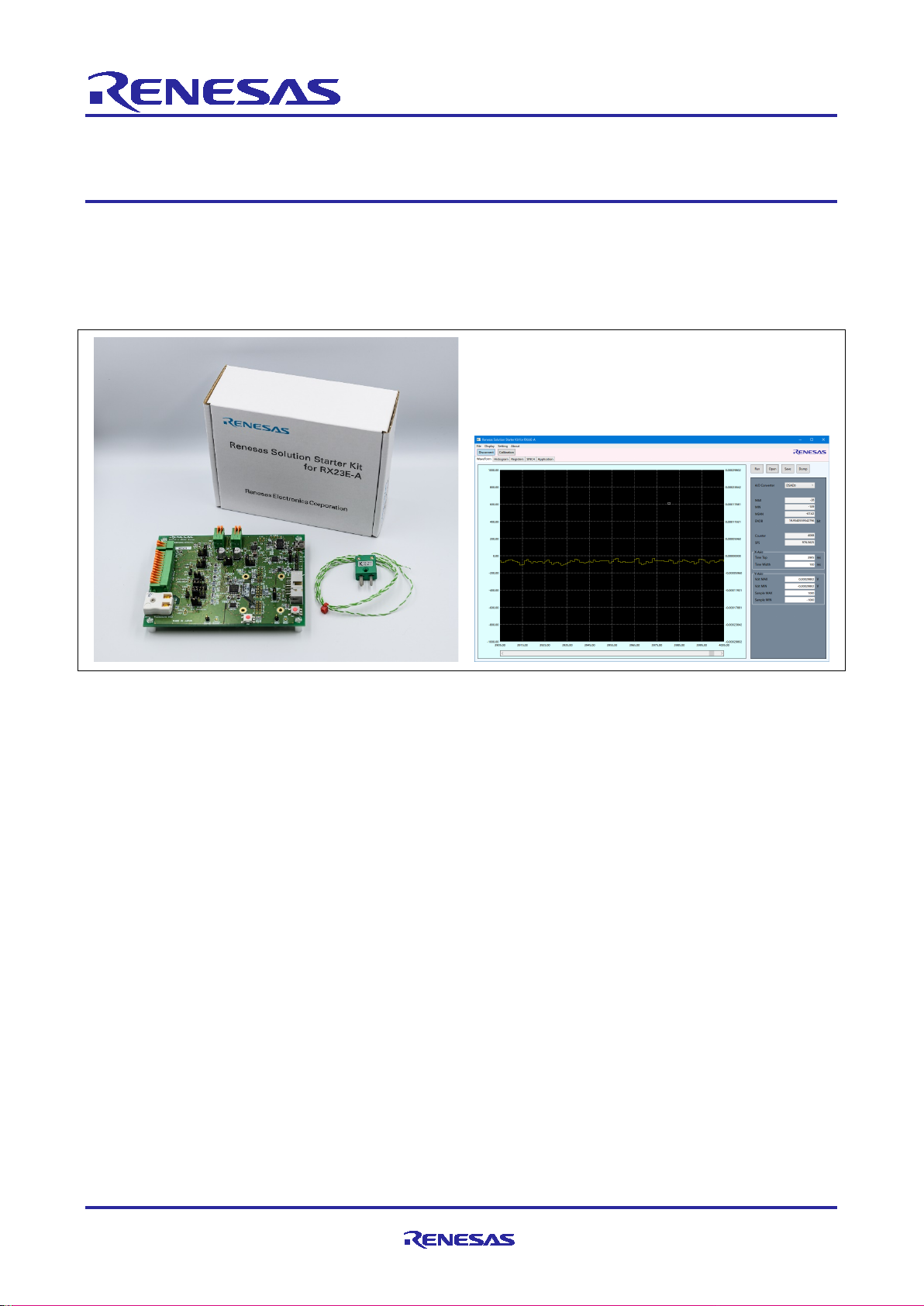
1. Overview
The Renesas Solution Starter Kit for RX23E-A (RSSKRX23E-A) an evaluation tool for sensor measurement
equipped with RX23E-A. Operation setting and A/D conversion value acquisition of RX23E-A can be done
with the PC tool program which is provided separately.
Figure 1-1 Renesas Solution Starter Kit for RX23E-A
2. Offering items
(1) RSSKRX23E-A board RTK0ESXB10C00001BJ
(2) RSSKRX23E-A User’s Manual R20UT4542EJ0100
(3) RSSKRX23E-A PC Tool Program R20AN0540EJ0100
(4) Quick Start Guide RSSKRX23E-A Renesas Solution Starter Kit for RX23E-A R20QS0007EJ0100
(This document)
Download the above (2) (3) (4) from Renesas Electronics web site.
R20QS0007EJ0100 Rev.1.00 Page 1 of 5
Nov.8.19
RSSKRX23E-A Renesas Solution Stater Kit for RX23E-A
Vd
RX23E-A
Vbus
LDO
Va
Vd
VLD O
JP1 4
JP1 5
Sy st e m Po we r
Selec t Jum per
Analo g Power
Selec t Jum per
Sy ste m Po wer Su pply
USB B us Pow er
Analo g Power S upp ly
VCC
E2 Lite
Emula tor Pow er Su pply
AVCC0
241
6
5
3
Vbus
1
2
3
CN7
CN8
CN4
CN5
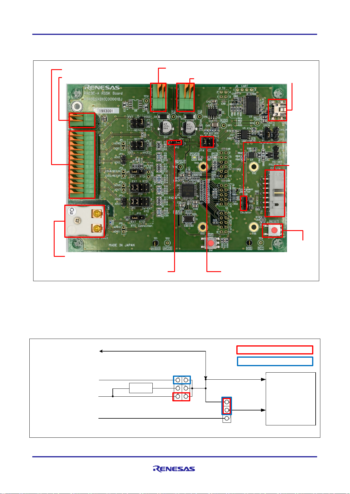
CN2: Signal input terminal
CN5: Analog Power Supply
CN4: System Power Supply
CN6:
CN7:
connector
JP15:
JP14:
CU mode
CN1: Power output terminal
default setting
USB Power supply setting
3. Configuration and Connection
3.1 Major Terminals and Jumpers
USB-Serial
connector
JP17:
M
select
jumper
Emulator
3.2 Power supply configuration
Power supply setting is “System Power Supply” as shipping default. USB Bus Power supply can be set
easily. Refer to the “2.2 Selecting Power Supplies” in “RSSKRX23E-A User’s Manual” for detail on Power
Supply Setting.
CN3: Thermocouple connector
Analog power select jumper
Figure 3-1 Major terminals and jumpers on RSSKRX23E-A board
SW2:
Reset
switch
System power select jumper
R20QS0007EJ0100 Rev.1.00 Page 2 of 5
Nov.8.19
Figure 3-2 Power supply configuration
RSSKRX23E-A Renesas Solution Stater Kit for RX23E-A
RSSKRX23E-A EVB
RX23E-A
USB-
Emulator
I/F
USB I/F
UART
(3Mbps)
USB 2.0FS
PC Tool
DC power
CN4
Operation buttons
3.3 System Connection
Supply 5V dc power for RSSKRX23E-A board default setting. Not require an external power supply on USB
power supply setting.
supply
System Power Supply
Program
COM
I/F
Figure 3-3 System Connection
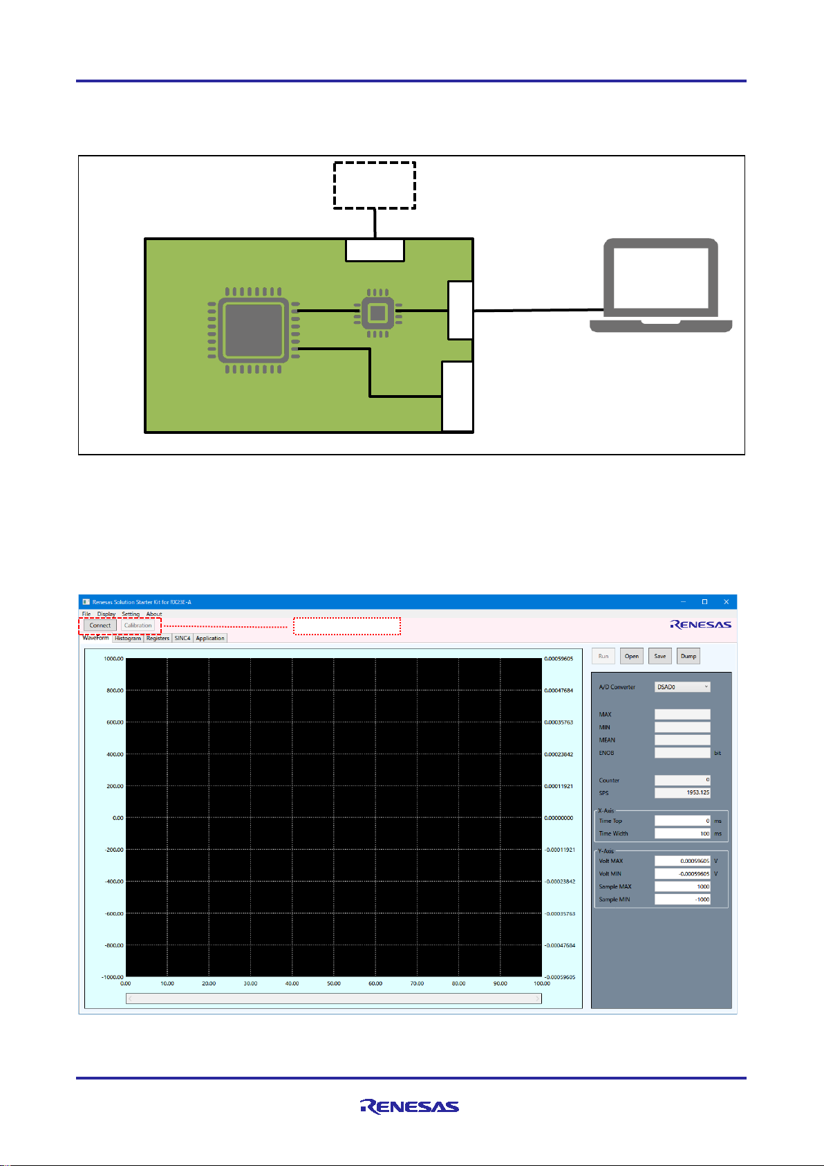
4. Software
4.1 PC tool program
Execute “RSSKRX23EA.exe” in “RSSKRX23E-A PC tool program” package. Refer to application note in the
package. About “connection” describes “2.2.1 Connection” in the application note, and A/D data collection
starts “Run” button in WaveForm TAB.
R20QS0007EJ0100 Rev.1.00 Page 3 of 5
Nov.8.19
Figure 4-1 PC tool program

RSSKRX23E-A Renesas Solution Stater Kit for RX23E-A
Select “RX200”
optional
Select “COM”
“Connect” after setting above
Select “rsskrx23ea_fw.mot”
Push “Start”
4.2 RX23E-A firmware
PC tool program and RX23E-A firmware work in pair. The firmware is stored in RX23E-A at the shipment.
When changing firmware for software development etc., re-write firmware “rsskrx23ea_fw.mot” which
includes “RSSKRX23EA PC tool program” package using Renesas Flash Programmer (RFP) V3.06.00 or
after. The Renesas Flash Programmer can be download from Renesas web site. Refer to the document of
Renesas Flash Programmer in detail.
The procedure is as follows:
1. Stop power supply to RSSKRX23E-A board, then set JP17(MCU mode select jumper) to “USB” (2-3).
2. Supply power to the board, then connect to PC by USB cable.
3. Execute Renesas Flash Programmer, then connect from menu “File” > “New Project…” in reference to
Figure 4-2.
4. Select “rsskrx23ea_fw.mot” file, then click “Start” after reset RSSKRX23E-A board.in reference to Figure
4-3.
5. Close Renesas Flash Programmer after writing correctly, and stop power supply to RSSKRX23E-A
board, then reset JP17(MCU mode select jumper) to “Emulator” (1-2).
Select COM port to use
Figure 4-2 RFP “Create new project”
R20QS0007EJ0100 Rev.1.00 Page 4 of 5
Nov.8.19
Figure 4-3 RFP Writing Operation

RSSKRX23E-A Renesas Solution Stater Kit for RX23E-A
Rev.
Date
Description
Page
Summary
1.00
Nov. 8, 19
1st edition
Revision History
R20QS0007EJ0100 Rev.1.00 Page 5 of 5
Nov.8.19

General Precautions in the Handling of Microprocessing Unit and Microcontroller
Unit Products
The following usage notes are applicable to all Microprocessing unit and Microcontroller unit products from Renesas. For detailed usage notes on the
products covered by this document, refer to the relevant sections of the document as well as any technical updates that have been issued for the products.
1. Precaution against Electrostatic Discharge (ESD)
A strong electrical field, when exposed to a CMOS device, can cause destruction of the gate oxide and ultimately degrade the device operation. Steps
must be taken to stop the generation of static electricity as much as possible, and quickly dissipate it when it occurs. Environmental control must be
adequate. When it is dry, a humidifier should be used. This is recommended to avoid using insulators that can easily build up static electricity.
Semiconductor devi ces must be stored and transported in an anti-static container, static shielding bag or conductive material. All test and
measurement tools including work benches and floors must be grounded. The operator must also be grounded using a wrist strap. Semiconductor
devices must not be touched with bare hands. Similar precautions must be taken for printed circuit boards with mounted semiconductor devices.
2. Processing at power-on
The state of the product is undefined at the time when power is supplied. The states of internal circuits in the LSI are indeterminate and the states of
register settings and pins are undefined at the time when power is supplied. In a finished product where the reset signal is applied to the external reset
pin, the states of pins are not guaranteed from the time when power is supplied until the reset process is completed. In a similar way, the states of pins
in a product that is reset by an on-chip power-on reset function are not guaranteed from the time when power is supplied until the power reaches the
level at which resetting is specified.
3. Input of signal during power-off state
Do not input signals or an I/O pull-up power supply while the device is powered off. The current injection that results from input of such a signal or I/O
pull-up power supply may cause malfunction and the abnormal current that passes in the device at this time may cause degradation of internal
elements. Follow the guideline for input signal during power-off state as described in your product documentation.
4. Handling of unused pins
Handle unused pins in accordance with the directions given under handling of unused pins in the manual. The input pins of CMOS products are
generally in the high-impedance state. In operation with an unused pin in the open-circuit state, extra electromagnetic noise is induced in the vicinity of
the LSI, an associated shoot-through current flows internally, and malfunctions occur due to the false recognition of the pin state as an input signal
become possible.
5. Clock signals
After applying a reset, only release the reset line after the operating clock signal becomes stable. When switching the clock signal during program
execution, wait until the target clock signal is stabilized. When the clock signal is generated with an external resonator or from an external oscillator
during a reset, ensure that the reset line is only released after full stabilization of the clock signal. Additionally, when switching to a clock signal
produced with an external resonator or by an external oscillator while program execution is in progress, wait until the target clock signal is stable.
6. Voltage application waveform at input pin
Waveform distortion due to input noise or a reflected wave may cause malfunction. If the input of the C MOS device stays in the area between V
(Max.) and V
input level is fixed, and also in the transition period when the input level passes through the area between V
7. Prohibition of access to reserved addresses
Access to reserved addresses is prohibited. The reserved addresses are provided for possible future expansion of functions. Do not access these
addresses as the correct operation of the LSI is not guaranteed.
8. Differences between products
Before changing from one product to another, for example to a product with a different part number, confirm that the change will not lead to problems.
The characteristics of a microprocessing unit or microcontroller unit products in the same group but having a different part number might differ in terms
of internal memory capacity, layout pattern, and other factors, which can affect the ranges of electrical characteristics, such as characteristic values,
operating margins, immunity to noise, and amount of radiated noise. When changing to a product with a different part number, implement a system-
evaluation test for the given product.
(Min.) due to noise, for example, the device may malfunction. Take care to prevent chattering noise from entering the device when the
IH
(Max.) and VIH (Min.).
IL
IL

Corporate Headquarters
Contact information
www.renesas.com
Trademarks
of their respective owners.
Notice
1. Descriptions of circuits, software and other related information in this document are provided only to illustrate the operation of semiconductor products
and application examples. You are fully responsible for the incorporation or any other use of the circuits, software, and information in the design of your
product or system. Renesas Electronics disclaims any and all liability for any losses and damages incurred by you or third parties arising from the use
of these circuits, software, or information.
2. Renesas Electronics hereby expressly disclaims any warranties against and liability for infringement or any other claims involving patents, copyrights,
or other intellectual property rights of third parties, by or arising from the use of Renesas Electronics products or technical information described in this
document, including but not limited to, the product data, drawings, charts, programs, algorithms, and application exam ples.
3. No license, express, implied or otherwise, is granted hereby under any patents, copyrights or other intellectual property rights of Renesas Electronics
or others.
4. You shall not alter, modify, copy, or reverse engineer any Renesas Electronics product, whether in whole or in part. Renesas Electronics disclaims any
and all liability for any losses or damages incurred by you or third parties arising from such alteration, modification, copying or reverse engineering.
5. Renesas Electronics products are classified according to the following two quality grades: “Standard” and “High Quality”. The intended applications for
each Renesas Electronics product depends on the product’s quality grade, as indicated below.
"Standard": Computers; office equipment; communications equipment; test and measurement equipment; audio and visual equipment; home
"High Quality": Transportation equipment (automobiles, trains, ships, etc.); traffic control (traffic lights); large-scale communication equipment; key
Unless expressly designated as a high reliability product or a product for harsh environments in a Renesas Electronics data sheet or other Renesas
Electronics document, Renesas Electronics products are not intended or authorized for use in products or systems that may pose a direct threat to
human life or bodily injury (artificial life support devices or systems; surgical implantations; etc.), or may cause serious property damage (space
system; undersea repeaters; nuclear power control systems; aircraft control systems; key plant systems; military equipment; etc.). Renesas Electronics
disclaims any and all liability for any damages or losses incurred by you or any third parties arising from the use of any Renesas Electronics product
that is inconsistent with any Renesas Electronics data sheet, user’s manual or other Renesas Electronics document.
6. When using Renesas Electronics products, refer to the latest product information (data sheets, user’s manuals, application notes, “General Notes for
Handling and Using Semiconductor Devices” in the reliability handbook, etc.), and ensure that usage conditions are within the ranges specified by
Renesas Electronics with respect to maximum ratings, operating power supply voltage range, heat dissipation characteristics, installation, etc. Renesas
Electronics disclaims any and all liability for any malfunctions, failure or accident arising out of the use of Renesas Electronics products outside of such
specified ranges.
7. Although Renesas Electronics endeavors to improve the quality and reliability of Renesas Electronics products, semiconductor products have specific
characteristics, such as the occurrence of failure at a certain rate and malfunctions under certain use conditions. Unless designated as a high reliability
product or a product for harsh environments in a Renesas Electronics data sheet or other Renesas Electronics document, Renesas Electronics
products are not subject to radiation resistance design. You are responsible for implementing safety measures to guard against the possibility of bodily
injury, injury or damage caused by fire, and/or danger to the public in the event of a failure or malfunction of Renesas Electronics products, such as
safety design for hardware and software, including but not limited to redundancy, fire control and malfunction prevention, appropriate treatment for
aging degradation or any other appropriate measures. Because the evaluation of microcomputer software alone is very difficult and impractical, you are
responsible for evaluating the safety of the final products or systems manufactured by you.
8. Please contact a Renesas Electronics sales office for details as to environmental matters such as the environmental compatibility of each Renesas
Electronics product. You are responsible for carefully and sufficiently investigating applicable laws and regulations that regulate the inclusion or use of
controlled substances, including without limitation, the EU RoHS Directive, and using Renesas Electronics products in compliance with all these
applicable laws and regulations. Renesas Electronics disclaims any and all liability for damages or losses occurring as a result of your noncompliance
with applicable law s and regulations.
9. Renesas Electronics products and technologies shall not be used for or incorporated into any products or systems whose manufacture, use, or sale is
prohibited under any applicable domestic or foreign laws or regulations. You shall comply with any applicable export control laws and regulations
promulgated and administered by the governments of any countries asserting jurisdiction over the parties or transactions.
10. It is the responsibility of the buyer or distributor of Renesas Electronics products, or any other party who distributes, disposes of, or otherwise sells or
transfers the product to a third party, to notify such third party in advance of the contents and conditions set forth in this document.
11. This document shall not be reprinted, reproduced or duplicated in any form, in whole or in part, without prior written consent of Renesas Electronics.
12. Please contact a Renesas Electronics sales office if you have any questions regarding the information contained in this document or Renesas
Electronics products.
(Note1) “Renesas Electronics” as used in this document means Renesas Electronics Corporation and also includes its directly or indirectly controlled
(Note2) “Renesas Electronics product(s)” means any product developed or manufactured by or for Renesas Electronics.
subsidiaries.
electronic appliances; machine tools; personal electronic equipment; industrial robots; etc.
financial terminal systems; safety control equipment; etc.
(Rev.4.0-1 November 2017)
TOYOSU FORESIA, 3-2-24 Toyosu,
Koto-ku, Tokyo 135-0061, Japan
Renesas and the Renesas logo are trademarks of Renesas Electronics
Corporation. All trademarks and registered trademarks are the property
For further information on a product, technology, the most up-to-date
version of a document, or your nearest sales office, please visit:
www.renesas.com/contact/
.
© 2019 Renesas Electronics Corporation. All rights reserved.
 Loading...