

Page 1

Application Note
RL78/G23
Voltage Detector
Introduction
This application note describes how to use the two voltage detectors (LVD) mounted on the RL78/G23 to
detect two voltage values.
Set voltage detector 0 (LVD0) to reset mode and voltage detector 1 (LVD1) to interrupt mode. When the
power supply voltage becomes lower than the voltage detected by voltage detector 1 (LVD1), the clock
frequency for the CPU and peripheral hardware changes to the frequency of the subsystem clock to reduce
power consumption.
Target Device
RL78/G23
When applying the sample program covered in this application note to another microcomputer, modify the
program according to the specifications for the target microcomputer and conduct an extensive evaluation of
the modified program.
R01AN5604EJ0100 Rev.1.00 Page 1 of 15
Apr.13.21
Page 2

RL78/G23 Voltage Detector
Contents
1. Specifications ............................................................................................................................. 3
1.1 Overview of Specifications ....................................................................................................................... 3
1.2 Outline of Operation ................................................................................................................................. 4
2. Operation Confirmation Conditions ............................................................................................ 6
3. Hardware Descriptions ............................................................................................................... 7
3.1 Example of Hardware Configuration ........................................................................................................ 7
3.2 List of Pins to be Used ............................................................................................................................. 7
4. Software Explanation ................................................................................................................. 8
4.1 Setting of Option Byte .............................................................................................................................. 8
4.2 List pf Constants ...................................................................................................................................... 8
4.3 List of Variables ....................................................................................................................................... 9
4.4 List of Functions ....................................................................................................................................... 9
4.5 Specification of Functions ........................................................................................................................ 9
4.6 Flowcharts .............................................................................................................................................. 10
4.6.1 Main Processing .................................................................................................................................. 10
4.6.2 Voltage Detector (LVD1) Interrupt Processing .................................................................................... 11
4.6.3 External Interrupt (INTP0) Processing ................................................................................................. 13
5. Sample Code ........................................................................................................................... 14
6. Reference Documents ............................................................................................................. 14
R01AN5604EJ0100 Rev.1.00 Page 2 of 15
Apr.13.21
Page 3
RL78/G23 Voltage Detector
Peripheral Function
Use
Voltage detector (LVD0, LVD1)
Monitor the power supply voltage (VDD).
External interrupt
Used as a pin edge detection interrupt (INTP0) by switch input.
(INTP0).
Port output
Controls the LEDs (LED1 to LED3) connected to P03, P02, and P43
pins.
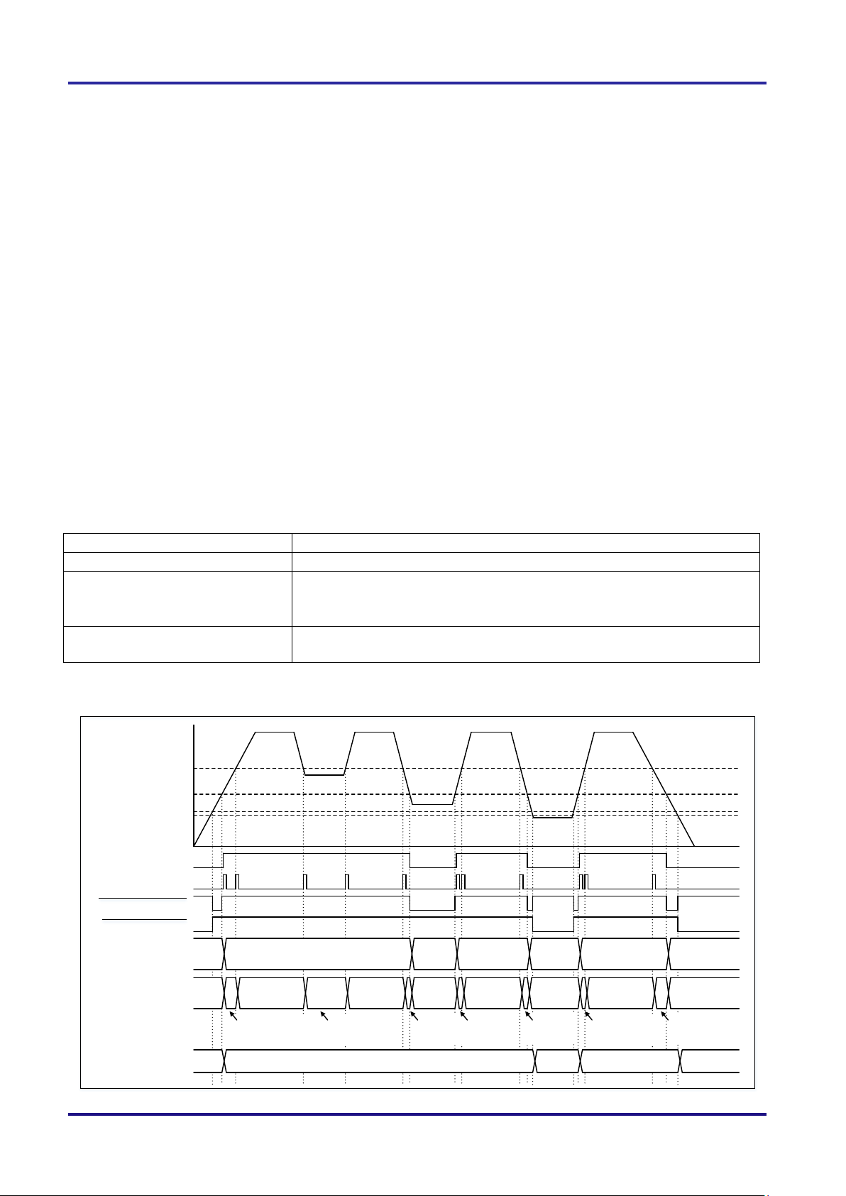
Power s upply voltage
(VDD)
V
LVD0
V
LVD1
V
PDR
INTL VI
LVD0 re set signal
POR rese t signa l
Res et
Operat ing Res et Operat ing
Res et
Operat ing Res et
CP U s ta tu s
Oper ating f requ ency
f
IH
32 MHz
Inactive
f
IH
32 MHz
Inactive
f
IH
32 MHz
Inactive
f
IH
32 MHz
Inactive
f
XT
32. 768 kHz
(After INTLVI
processing)
f
XT
32. 768 kHz
f
XT
32. 768 kHz
f
XT
32. 768 kHz
f
XT
32. 768 kHz
f
XT
32. 768 kHz
RAM st atus
RA M d ata ret ained
Not
determined
RA M d ata ret ained
Not
determined
Not
determined
LVD1EN
f
XT
32. 768
kHz
(After INTLVI
processing)
1. Specifications
1.1 Overview of Specifications
In this application note, three LEDs are used. When the CPU is operating, one LED keeps flashing. Each time
the switch is pressed, the flashing LED changes to another LED.
Set voltage detector 0 (LVD0) to reset mode and voltage detector 1 (LVD1) to interrupt mode.
When the power supply voltage (V
) equals or exceeds the voltage detected by LVD0 (V
DD
operates at 32 MHz and flashes an LED. When V
operation clock (f
When V
equals or exceeds V
DD
) changes to 32.768 kHz. As a result, the flashing interval of the LED becomes longer.
CLK
LVD1
again, f
changes to 32 MHz. In this case, the flashing interval of the LED
CLK
falls below the voltage detected by LVD1 (V
DD
), the CPU
LVD0
LVD1
), the CPU
becomes shorter.
When V
than V
in the RAM is retained. When V
equals or exceeds the voltage detected by the power-on reset (POR) circuit (V
DD
, LVD0 generates an internal reset signal and the LED goes off. In this voltage range, the data stored
LVD0
equals or exceeds V
DD
again, the LED that used to flash before the reset
LVD0
) and is lower
PDR
resumes flashing.
When V
falls below the voltage detected by the POR circuit (V
DD
reset signal and the LED goes off. In this case, the data stored in the RAM is not retained. When V
exceeds V
again, LED1 starts flashing.
LVD0
), the POR circuit generates an internal
PDR
equals or
DD
Table 1-1 lists the peripheral functions to be used and their uses, and Figure 1-1 gives an overview of the
voltage detector (LVD) operation.
Table 1-1 Peripheral Functions Used and Their Uses
Receives switch input interrupts on the edge-detecting interrupt input pin
Figure 1-1 Overview of the Voltage Detector (LVD) Operation
R01AN5604EJ0100 Rev.1.00 Page 3 of 15
Apr.13.21
Page 4
RL78/G23 Voltage Detector
LED On/Off Status
LED1
LED2
LED3
(1)
OFF
OFF
OFF
(2)
ON (flashing)
OFF
OFF
(3)
OFF
ON (flashing)
OFF
(4)
OFF
OFF
ON (flashing)
1.2 Outline of Operation
Set LVD0 to reset mode and LVD1 to interrupt mode.
changes depending on VDD. You can determine whether f
f
CLK
is changed by checking the flashing interval
CLK
of the LED.
When V
When V
LVD1
LVD0
≦ VDD: f
≦ V
DD
= 32 MHz, shorter LED flashing interval
CLK
< V
LVD1
: f
= 32.768 kHz, longer LED flashing interval
CLK
The LEDs cycle as follows each time the switch is pressed.
LED1 → LED2 → LED3 → LED1 →・・・
Table 1-2 LED On/Off Status
Operation
Operations (2) to (4) cycle each time the switch is pressed.
When LVD0 generates a reset signal, the data stored in the RAM (the number of switch inputs) is retained.
When the CPU resumes operation, the LED that used to flash before the reset is selected.
When the POR circuit generates a reset signal, the data stored in the RAM (the number of switch inputs) is
not retained. When the CPU resumes operation, LED1 is selected.
(1) Initialize the voltage detector (LVD).
<Setting conditions>
At power-on or after a reset release, the option bytes are automatically referenced and LVD0 is set to reset
mode.
Set the LVD0 detection voltage to 1.875 V (rising) and to 1.835 V (falling).
Set LVD1 to interrupt mode.
Set the LVD1 detection voltage to 2.400 V (rising) and to 2.350 V (falling).
(2) Set the I/O ports.
P03, P02, and P43 pins: Set as output ports (to be used for LED control).
P137 / INTP0 pin: Set as an input port (to be used for switch input).
(3) Initialize external interrupt processing.
Set the falling edge as the valid edge for the INTP0 pin and enable switch input.
Enable INTP0 interrupts.
R01AN5604EJ0100 Rev.1.00 Page 4 of 15
Apr.13.21
Page 5

RL78/G23 Voltage Detector
;--------------------------------------------------
Comment out
__no_init uint8_t g_SwCount; /* Counter for KEY pushed */
(4) Flash the LED corresponding to the input count of the switch.
When the switch is pressed, the falling edge of the P137 / INTP0 pin is detected and interrupt processing
is performed.
To prevent chattering, the voltage applied to the P137 pin is checked approximately every 5 ms. When the
switch is determined to be pressed, the switch input count is updated and the LED corresponding to the
switch input count flashes (see Table 1-2).
(5) f
changes based on the voltage detected by LVD1.
CLK
When V
When V
LVD1
LVD0
≦ VDD: f
≦ V
DD
= 32 MHz
CLK
< V
LVD1
: f
= 32.768 kHz
CLK
When LVD0 generates a reset signal, the data stored in the RAM (switch input count) is retained. However, if
you use the startup routine prepared in CS+ or e2studio without modifying it, the data in the internal RAM is
initialized before the main functions. To prevent this, comment out the initialization program for the internal
RAM data.
; initializing BSS
;------------------------------------------------- ; clear external variables which doesn't have initial value (near)
; MOVW HL,#LOWW(STARTOF(.bss))
; MOVW AX,#LOWW(STARTOF(.bss) + SIZEOF(.bss))
; BR $.L2_BSS
;.L1_BSS:
; MOV [HL+0],#0
; INCW HL
;.L2_BSS:
; CMPW AX,HL
; BNZ $.L1_BSS
If you use the startup routine prepared in IAR Embedded Workbench without modifying it, the data in the
internal RAM is initialized before the main functions. To prevent this, add __no_init when you declare variables,
and place the data in the area for holding variable values.
Caution For details about the cautions on using the device, see the RL78/G23 User’s Manual: Hardware.
R01AN5604EJ0100 Rev.1.00 Page 5 of 15
Apr.13.21
Page 6

RL78/G23 Voltage Detector
Item
Description
MCU used
RL78/G23 (R7F100GLG)
Operating frequency
• High-speed on-chip oscillator clock (fIH): 32 MHz
• Subsystem clock (XT1 clock (fXT)): 32.768 kHz
Operating voltage
5.0 V (can be operated at 2.0 V to 5.5 V)
At falling edge TYP. 2.35 V (2.30 V to 2.40 V)
Integrated development
environment (CS+)
CS+ for CC V8.05.00f from Renesas Electronics Corp.
C compiler (CS+)
CC-RL V1.09.00 from Renesas Electronics Corp.
Integrated development
environment (e2studio)
e2studio V2021-01 from Renesas Electronics Corp.
C compiler (e2studio)
CC-RL V1.09.00 from Renesas Electronics Corp.
Integrated development
environment (IAR)
IAR Embedded Workbench for Renesas RL78 V4.20.1 from IAR Systems
Corp.
C compiler (IAR)
IAR C/C++ Compiler for Renesas RL78 V4.20.1.2260 from IAR Systems
Corp.
Board used
RL78/G23 Fast Prototyping Board
2. Operation Confirmation Conditions
The operation of the sample code provided with this application note has been tested under the following
conditions.
Table 2-1
Operation Confirmation Conditions
LVD0 detection voltage: Reset mode
At rising edge TYP. 1.90 V (1.84 V to 1.95 V)
At falling edge TYP. 1.86 V (1.80 V to 1.91 V)
LVD1 detection voltage: Interrupt mode
At rising edge TYP. 2.40 V (2.35 V to 2.45 V)
R01AN5604EJ0100 Rev.1.00 Page 6 of 15
Apr.13.21
Page 7

RL78/G23 Voltage Detector
RESET
P40 / TOOL0
V
DD
For on-chip debug
RL78/G23
V
DD
/EV
DD
REG C
VSS/EV
SS
P137 / INTP0
V
DD
V
DD
LED2
P02
LED1
P03
LED3
P43
XT2
XT1
XT1
32.768 kHz
Pin name
I/O
Function
P03
Output
LED1 control
P02
Output
LED2 control
P43
Output
LED3 control
P137 / INTP0
Input
LED status switching
XT1
Input
Subsystem clock input: 32.768 kHz
XT2
Input
Subsystem clock input: 32.768 kHz
3. Hardware Descriptions
3.1 Example of Hardware Configuration
Figure 3-1 shows an example of the hardware configuration used in the application note.
Figure 3-1 Hardware Configuration
Note 1. This simplified circuit diagram was created to show an overview of connections only. When
actually designing your circuit, make sure the design includes appropriate pin handling and meets
electrical characteristic requirements (connect each input-only port to V
DD or VSS through a
resistor.)
Note 2. Connect any pins whose name begins with EV
to VDD, respectively.
EV
DD
Note 3. V
DD must not be lower than the interrupt generation voltage (VLVD1) that is specified for the LVD1.
SS
to V
and any pins whose name begins with
SS,
3.2 List of Pins to be Used
Table 3-1 lists the pins to be used and their functions.
Table 3-1 Pins to be Used and Their Functions
Caution In this application note, only the used pins are processed. When actually designing your circuit,
make sure the design includes sufficient pin processing and meets electrical characteristic
requirements.
R01AN5604EJ0100 Rev.1.00 Page 7 of 15
Apr.13.21
Page 8

RL78/G23 Voltage Detector
Address
Setting Value
Contents
000C0H / 040C0H
11101111B
Disables the watchdog timer.
(Counting stopped after reset)
000C1H / 040C1H
11111110B
LVD0 detection voltage: reset mode
At falling edge TYP. 1.86 V (1.80 V to 1.91 V)
000C2H / 040C2H
11101000B
HS mode,
High-speed on-chip oscillator clock (fIH): 32 MHz
000C3H / 040C3H
10000101B
Enables on-chip debugging
Constant Name
Setting Value
Description
LED_ON
01H
LED control: On
LED_OFF
00H
LED control: Off
WAITCOUNT_32M
8000
Wait count for 5 ms when the high-speed on-chip
oscillator clock operates at 32 MHz
WAITCOUNT_32K
8
Wait count for 5 ms when the subsystem clock
operates at 32.768 kHz
4. Software Explanation
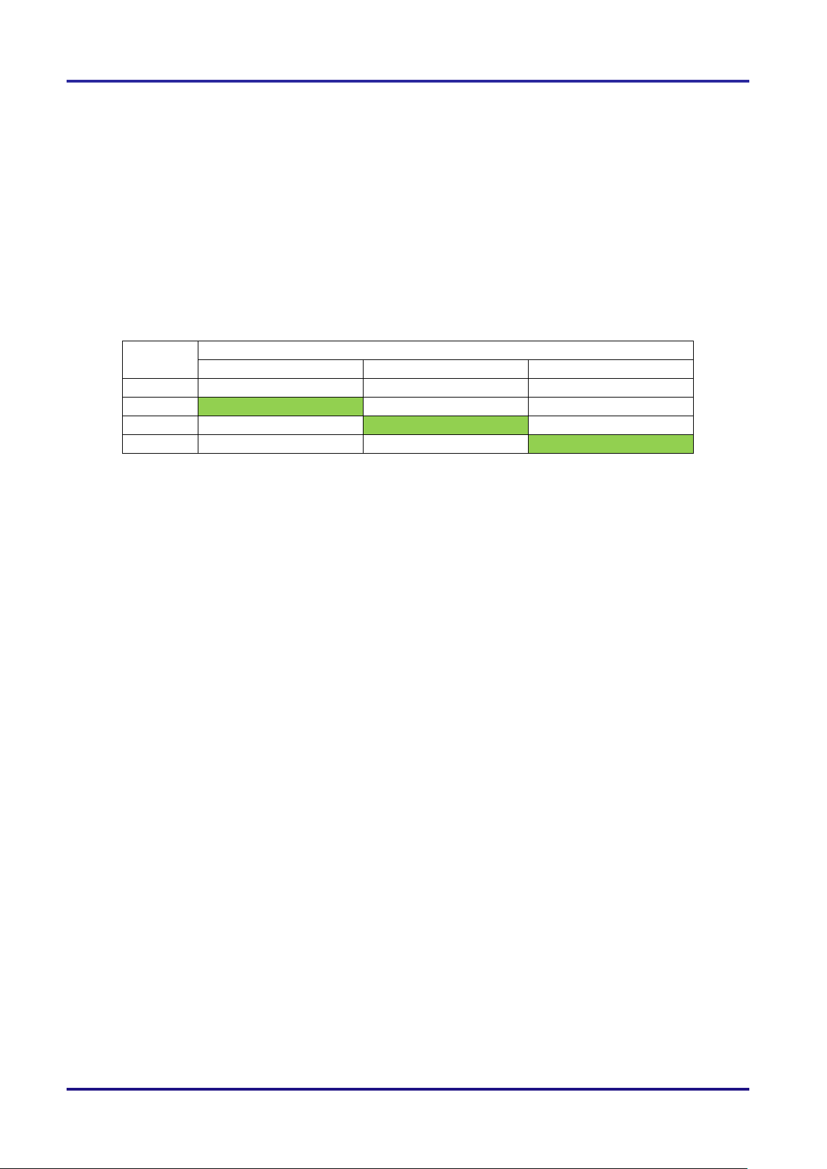
4.1 Setting of Option Byte
Table 4-1 shows the option byte settings. Set the values that are most suited to your system as necessary.
Table 4-1 Option Byte Settings
At rising edge TYP. 1.90 V (1.84 V to 1.95 V)
4.2 List pf Constants
Table 4-2 lists the constants that are used in the sample code.
Table 4-2 Constants
R01AN5604EJ0100 Rev.1.00 Page 8 of 15
Apr.13.21
Page 9

RL78/G23 Voltage Detector
Type
Variable Name
Description
Function Used
uint8_t
g_SwCount
Switch transition status
variable
main
(),r_Config_INTC_intp0_interrupt ()
uint8_t
aLedNumberTable
LED ON pattern table
main ()
Function Name
Outline
r_Config_INTC_intp0_interrupt()
External interrupt (INTP0) processing.
r_lvd_interrupt()
Voltage detector (LVD1) interrupt processing.
r_Config_INTC_intp0_interrupt()
Outline
External interrupt (INTP0) processing.
Header
r_cg_macrodriver.h, r_cg_userdefine.h, Config_INTC.h
Declaration
static void __near r_Config_INTC_intp0_interrupt (void)
Description
Changes the LEDs to flash each time the switch is pressed.
Argument
None
Return Value
None
r_lvd_interrupt()
Outline
Voltage detector (LVD1) interrupt processing.
Header
r_cg_macrodriver.h, r_cg_userdefine.h
Declaration
static void __near r_lvd_interrupt (void)
Description
Changes the operating clock depending on the value of VDD. When V
< V
, the
clock.
Argument
None
Return Value
None
4.3 List of Variables
Table 4-3 lists global variables.
Table 4-3 Global Variables
4.4 List of Functions
Table 4-4 shows a list of functions.
Table 4-4 Functions
4.5 Specification of Functions
The function specifications of the sample code are shown below.
high-speed on-chip oscillator clock is replaced by the subsystem clock. When
≧ V
V
DD
, the subsystem clock is replaced by the high-speed on-chip oscillator
LVD1
DD
LVD1
R01AN5604EJ0100 Rev.1.00 Page 9 of 15
Apr.13.21
Page 10

RL78/G23 Voltage Detector
ma in
Disable parity error resets
RPECTL register
RPERDIS bit
← 1
Is internal reset generated
by voltage detector?
NO
YES
Set 0 as SW inp ut count
: while(1) loop
LEDs 1 to 3 on/off co ntrol
Extern al inter rup t (INTP0)
Interrupt request sig nal gene ra ted by LVD1
(IN TLVI)
P03 (LED1) , P02 (LED2) , P43 (LED3)
Reference LED control table to determ ine LED
on/off status
INTP0 interrup t enable process ing
r_Config_INTC_INTP0_Start
LVD1 operation start processing
r_Config_L VD1_Start
IE←1
Enable interrupt
4.6 Flowcharts
4.6.1 Main Processing
Figure 4-1 shows the flowchart of the main processing.
Figure 4-1 Main Processing
R01AN5604EJ0100 Rev.1.00 Page 10 of 15
Apr.13.21
Page 11

RL78/G23 Voltage Detector
r_lvd_interrupt
return
A
B
XT1 oscillato
r: wait for oscillation stability
Is high-speed on-chip oscill ator
clock stop condition* satisfied?
*Condition: MCS1 bit = 1 or
MCS bit = 1 or
CLS bit = 1
NO
YES
Is switch to subsystem clo ck (f
XT
)*
complete ?
*Condition: CLS bit = 1
NO
YES
XT1 oscillator: operation starts
CSC register
XTSTOP bit ← 0
CKC register
CSS bit ← 1
Change CPU/peripheral hardware clock (f
CLK
)
to subsystem clock (f
XT
)
High-speed on-chip oscillator cl ock: operation stopped
CSC register
HIOSTOP bit ← 1
Voltage detection flag (LVD1F)
LVD1F = 1 (V
DD
< V
LVD1
)
LVD1F = 0 (V
DD
≧ V
LVD1
)
4.6.2 Voltage Detector (LVD1) Interrupt Processing
Figure 4-2 and Figure 4-3 show flowcharts of the Voltage detector (LVD1) interrupt processing.
Figure 4-2
Voltage Detector (LVD1) Interrupt Processing. (1/2)
R01AN5604EJ0100 Rev.1.00 Page 11 of 15
Apr.13.21
Page 12

RL78/G23 Voltage Detector
A
B
High-speed on
-chip oscillator clock: wait for oscillation stability
CSC register
HIOSTOP bit ← 0
High
-speed on
-chip oscillator clock: operation starts
Change CPU/peripheral hardware clock (f
CLK
)
to main s ystem clock (f
MAIN
)
CKC register
CSS bit ← 0
NO
YES
Is switch to main syst em cl ock (f
MAIN
)* complete?
*Condition: CLS bit = 0
Select main on-chip oscillator clock (f
OCO
)
as main system clock (f
MAIN
)
CKC register
MCM0 bit
← 0
CKC register
MCM1 bit
← 0
Select high-speed on-chip oscillator cl ock (fIH)
as main on-chip oscillator clock (f
OCO
)
NO
YES
Is switch to high-speed on-chip oscillator
clock (fIH)* complete?
*Condition: MCS bit = 0 and
MCS1 bit = 0
YES
NO
*Condition: CLS bit = 0
Is subsystem clock (fXT) stop condition* satisfied?
CSC register
XTSTOP bit ← 1
XT1 oscillator: operation stopped
Figure 4-3 Voltage Detector (LVD1) Interrupt Processing (2/2)
R01AN5604EJ0100 Rev.1.00 Page 12 of 15
Apr.13.21
Page 13

RL78/G23 Voltage Detector
r_Config_ INTC_in tp0_interrupt()
Upda te SW input coun t
return
Chattering prevention processing
g_SwCount = 0→1
→2→3→1→・・・
4.6.3 External Interrupt (INTP0) Processing
Figure 4-4 shows the flowchart of the external interrupt (INTP0) processing
Figure 4-4
External Interrupt (INTP0) Processing
R01AN5604EJ0100 Rev.1.00 Page 13 of 15
Apr.13.21
Page 14

RL78/G23 Voltage Detector
5. Sample Code
Sample code can be downloaded from the Renesas Electronics website.
6. Reference Documents
RL78/G23 User’s Manual: Hardware (R01UH0896J)
RL78 family user's manual software (R01US0015J)
The latest versions can be downloaded from the Renesas Electronics website.
Technical update
The latest versions can be downloaded from the Renesas Electronics website.
All trademarks and registered trademarks are the property of their respective owner.
R01AN5604EJ0100 Rev.1.00 Page 14 of 15
Apr.13.21
Page 15

RL78/G23 Voltage Detector
Rev.
Date
Description
Page
Summary
1.00
2021.04.13
First Edition
Revision History
―
R01AN5604EJ0100 Rev.1.00 Page 15 of 15
Apr.13.21
Page 16

RL78/G23 Voltage Detector
General Precautions in the Handling of Microprocessing Unit and Microcontroller
Unit Products
The following usage notes are applicable to all Microprocessing unit and Microcontroller unit products from Renesas. For detailed usage notes on the
products covered by this document, refer to the relevant sections of the document as well as any technical updates that have been issued for the products.
1. Precaution against Electrostatic Discharge (ESD)
A strong electrical field, when exposed to a CMOS device, can cause destruction of the gate oxide and ultimately degrade the device operation. Steps
must be taken to stop the generation of static electricity as much as possible, and quickly dissipate it when it occurs. Environmental control must be
adequate. When it is dry, a humidifier should be used. This is recommended to avoid using insulators that can easily build up static electricity.
Semiconductor devices must be stored and transported in an anti-static container, static shielding bag or conductive material. All test and measurement
tools including work benches and floors must be grounded. The operator must also be grounded using a wrist strap. Semiconductor devices must not be
touched with bare hands. Similar precautions must be taken for printed circuit boards with mounted semiconductor devices.
2. Processing at power-on
The state of the product is undefined at the time when power is supplied. The states of internal circuits in the LSI are indeterminate and the states of
register settings and pins are undefined at the time when power is supplied. In a finished product where the reset signal is applied to the external reset
pin, the states of pins are not guaranteed from the time when power is supplied until the reset process is completed. In a similar way, the states of pins in
a product that is reset by an on-chip power-on reset function are not guaranteed from the time when power is supplied until the power reaches the level
at which resetting is specified.
3. Input of signal during power-off state
Do not input signals or an I/O pull-up power supply while the device is powered off. The current injection that results from input of such a signal or I/O
pull-up power supply may cause malfunction and the abnormal current that passes in the device at this time may cause degradation of internal elements.
Follow the guideline for input signal during power-off state as described in your product documentation.
4. Handling of unused pins
Handle unused pins in accordance with the directions given under handling of unused pins in the manual. The input pins of CMOS products are
generally in the high-impedance state. In operation with an unused pin in the open-circuit state, extra electromagnetic noise is induced in the vicinity of
the LSI, an associated shoot-through current flows internally, and malfunctions occur due to the false recognition of the pin state as an input signal
become possible.
5. Clock signals
After applying a reset, only release the reset line after the operating clock signal becomes stable. When switching the clock signal during program
execution, wait until the target clock signal is stabilized. When the clock signal is generated with an external resonator or from an external oscillator
during a reset, ensure that the reset line is only released after full stabilization of the clock signal. Additionally, when switching to a clock signal produced
with an external resonator or by an external oscillator while program execution is in progress, wait until the target clock signal is stable.
6. Voltage application waveform at input pin
Waveform distortion due to input noise or a reflected wave may cause malfunction. If the input of the CMOS device stays in the area between V
and V
(Min.) due to noise, for example, the device may malfunction. Take care to prevent chattering noise from entering the device when the input level
IH
is fixed, and also in the transition period when the input level passes through the area between V
7. Prohibition of access to reserved addresses
Access to reserved addresses is prohibited. The reserved addresses are provided for possible future expansion of functions. Do not access these
addresses as the correct operation of the LSI is not guaranteed.
8. Differences between products
Before changing from one product to another, for example to a product with a different part number, confirm that the change will not lead to problems.
The characteristics of a microprocessing unit or microcontroller unit products in the same group but having a different part number might differ in terms
of internal memory capacity, layout pattern, and other factors, which can affect the ranges of electrical characteristics, such as characteristic values,
operating margins, immunity to noise, and amount of radiated noise. When changing to a product with a different part number, implement a
system-evaluation test for the given product.
(Max.) and VIH (Min.).
IL
(Max.)
IL
R01AN5604EJ0100 Rev.1.00 Page 1 of 15
Apr.13.21
Page 17

RL78/G23 Voltage Detector
Corporate Headquarters
Contact information
Trademarks
Renesas and the Renesas logo are trademarks of Renesas Electronics
Notice
1. Descriptions of circuits, software and other related information in this document are provided only to illustrate the operation of semiconductor products
and application examples. You are fully responsible for the incorporation or any other use of the circuits, software, and information in the design of your
product or system. Renesas Electronics disclaims any and all liability for any losses and damages incurred by you or third parties arising from the use of
these circuits, software, or information.
2. Renesas Electronics hereby expressly disclaims any warranties against and liability for infringement or any other claims involving patents, copyrights, or
other intellectual property rights of third parties, by or arising from the use of Renesas Electronics products or technical information described in this
document, including but not limited to, the product data, drawings, charts, programs, algorithms, and application examples.
3. No license, express, implied or otherwise, is granted hereby under any patents, copyrights or other intellectual property rights of Renesas Electronics or
others.
4. You shall be responsible for determining what licenses are required from any third parties, and obtaining such licenses for the lawful import, export,
manufacture, sales, utilization, distribution or other disposal of any products incorporating Renesas Electronics products, if required.
5. You shall not alter, modify, copy, or reverse engineer any Renesas Electronics product, whether in whole or in part. Renesas Electronics disclaims any
and all liability for any losses or damages incurred by you or third parties arising from such alteration, modification, copying or reverse engineering.
6. Renesas Electronics products are classified according to the following two quality grades: “Standard” and “High Quality”. The intended applications for
each Renesas Electronics product depends on the product’s quality grade, as indicated below.
"Standard": Computers; office equipment; communications equipment; test and measurement equipment; audio and visual equipment; home
"High Quality": Transportation equipment (automobiles, trains, ships, etc.); traffic control (traffic lights); large-scale communication equipment; key
Unless expressly designated as a high reliability product or a product for harsh environments in a Renesas Electronics data sheet or other Renesas
Electronics document, Renesas Electronics products are not intended or authorized for use in products or systems that may pose a direct threat to
human life or bodily injury (artificial life support devices or systems; surgical implantations; etc.), or may cause serious property damage (space system;
undersea repeaters; nuclear power control systems; aircraft control systems; key plant systems; military equipment; etc.). Renesas Electronics
disclaims any and all liability for any damages or losses incurred by you or any third parties arising from the use of any Renesas Electronics product that
is inconsistent with any Renesas Electronics data sheet, user’s manual or other Renesas Electronics document.
7. No semiconductor product is absolutely secure. Notwithstanding any security measures or features that may be implemented in Renesas Electronics
hardware or software products, Renesas Electronics shall have absolutely no liability arising out of any vulnerability or security breach, including but not
limited to any unauthorized access to or use of a Renesas Electronics product or a system that uses a Renesas Electronics product. RENESAS
ELECTRONICS DOES NOT WARRANT OR GUARANTEE THAT RENESAS ELECTRONICS PRODUCTS, OR ANY SYSTEMS CREATED USING
RENESAS ELECTRONICS PRODUCTS WILL BE INVULNERABLE OR FREE FROM CORRUPTION, ATTACK, VIRUSES, INTERFERENCE,
HACKING, DATA LOSS OR THEFT, OR OTHER SECURITY INTRUSION (“Vulnerability Issues”). RENESAS ELECTRONICS DISCLAIMS ANY AND
ALL RESPONSIBILITY OR LIABILITY ARISING FROM OR RELATED TO ANY VULNERABILITY ISSUES. FURTHERMORE, TO THE EXTENT
PERMITTED BY APPLICABLE LAW, RENESAS ELECTRONICS DISCLAIMS ANY AND ALL WARRANTIES, EXPRESS OR IMPLIED, WITH
RESPECT TO THIS DOCUMENT AND ANY RELATED OR ACCOMPANYING SOFTWARE OR HARDWARE, INCLUDING BUT NOT LIMITED TO
THE IMPLIED WARRANTIES OF MERCHANTABILITY, OR FITNESS FOR A PARTICULAR PURPOSE.
8. When using Renesas Electronics products, refer to the latest product information (data sheets, user’s manuals, application notes, “General Notes for
Handling and Using Semiconductor Devices” in the reliability handbook, etc.), and ensure that usage conditions are within the ranges specified by
Renesas Electronics with respect to maximum ratings, operating power supply voltage range, heat dissipation characteristics, installation, etc. Renesas
Electronics disclaims any and all liability for any malfunctions, failure or accident arising out of the use of Renesas Electronics products outside of such
specified ranges.
9. Although Renesas Electronics endeavors to improve the quality and reliability of Renesas Electronics products, semiconductor products have specific
characteristics, such as the occurrence of failure at a certain rate and malfunctions under certain use conditions. Unless designated as a high reliability
product or a product for harsh environments in a Renesas Electronics data sheet or other Renesas Electronics document, Renesas Electronics
products are not subject to radiation resistance design. You are responsible for implementing safety measures to guard against the possibility of bodily
injury, injury or damage caused by fire, and/or danger to the public in the event of a failure or malfunction of Renesas Electronics products, such as
safety design for hardware and software, including but not limited to redundancy, fire control and malfunction prevention, appropriate treatment for
aging degradation or any other appropriate measures. Because the evaluation of microcomputer software alone is very difficult and impractical, you are
responsible for evaluating the safety of the final products or systems manufactured by you.
10. Please contact a Renesas Electronics sales office for details as to environmental matters such as the environmental compatibility of each Renesas
Electronics product. You are responsible for carefully and sufficiently investigating applicable laws and regulations that regulate the inclusion or use of
controlled substances, including without limitation, the EU RoHS Directive, and using Renesas Electronics products in compliance with all these
applicable laws and regulations. Renesas Electronics disclaims any and all liability for damages or losses occurring as a result of your noncompliance
with applicable laws and regulations.
11. Renesas Electronics products and technologies shall not be used for or incorporated into any products or systems whose manufacture, use, or sale is
prohibited under any applicable domestic or foreign laws or regulations. You shall comply with any applicable export control laws and regulations
promulgated and administered by the governments of any countries asserting jurisdiction over the parties or transactions.
12. It is the responsibility of the buyer or distributor of Renesas Electronics products, or any other party who distributes, disposes of, or otherwise sells or
transfers the product to a third party, to notify such third party in advance of the contents and conditions set forth in this document.
13. This document shall not be reprinted, reproduced or duplicated in any form, in whole or in part, without prior written consent of Renesas Electronics.
14. Please contact a Renesas Electronics sales office if you have any questions regarding the information contained in this document or Renesas
Electronics products.
(Note1) “Renesas Electronics” as used in this document means Renesas Electronics Corporation and also includes its directly or indirectly controlled
(Note2) “Renesas Electronics product(s)” means any product developed or manufactured by or for Renesas Electronics.
subsidiaries.
electronic appliances; machine tools; personal electronic equipment; industrial robots; etc.
financial terminal systems; safety control equipment; etc.
(Rev.5.0-1 October 2020)
TOYOSU FORESIA, 3-2-24 Toyosu,
Koto-ku, Tokyo 135-0061, Japan
www.renesas.com
Corporation. All trademarks and registered trademarks are the property
of their respective owners.
For further information on a product, technology, the most up-to-date
version of a document, or your nearest sales office, please visit:
www.renesas.com/contact/
.
© 2021 Renesas Electronics Corporation. All rights reserved.
 Loading...