

Page 1

Application Note
RL78/G13, RL78/G23
Migration Guide from RL78/G13 to RL78/G23
Introduction
This application note describes the differences in peripheral functions between RL78/G13 and RL78/G23.
Target Device
RL78/G13, RL78/G23
For detailed information on peripheral functions and electrical characteristics, refer to the User's Manual:
Hardware and Technical Updates.
When using this application note with other Renesas MCUs, careful evaluation is recommended after making
modifications to comply with the alternate MCU.
R01AN5378EJ0100 Rev.1.00 Page 1 of 24
Apr.13.21
Page 2

RL78/G13, RL78/G23 Migration Guide from RL78/G13 to RL78/G23
Contents
1. Differences in peripheral functions between RL78/G13 and RL78/G23.................................... 3
2. Comparison of RL78/G13 and RL78/G23 registers .................................................................. 6
2.1 Port Functions ......................................................................................................................................... 6
2.2 Clock Generator ...................................................................................................................................... 8
2.3 Timer Array Unit ...................................................................................................................................... 9
2.4 Realtime Clock ...................................................................................................................................... 10
2.5 Clock Output/Buzzer Output Controller ................................................................................................. 11
2.6 Watchdog Timer .................................................................................................................................... 11
2.7 A/D Converter ........................................................................................................................................ 12
2.8 Serial Array Unit .................................................................................................................................... 13
2.9 Serial Interface IICA .............................................................................................................................. 15
2.10 Interrupt Functions................................................................................................................................. 16
2.11 Key Interrupt Function ........................................................................................................................... 17
2.12 Standby Function................................................................................................................................... 17
2.13 Reset Function ...................................................................................................................................... 18
2.14 Power-On-Reset Circuit ........................................................................................................................ 18
2.15 Voltage Detector .................................................................................................................................... 19
2.16 Safety Functions .................................................................................................................................... 20
2.17 Regulator ............................................................................................................................................... 20
2.18 Option Bytes .......................................................................................................................................... 21
2.19 On-Chip Debugging ............................................................................................................................... 21
2.20 BCD Correction Circuit .......................................................................................................................... 21
3. Other changes and notes ...................................................................................................... 22
3.1 RL78/G23 instruction set ....................................................................................................................... 22
4. Documents for Reference ...................................................................................................... 23
Revision History ............................................................................................................................ 24
R01AN5378EJ0100 Rev.1.00 Page 2 of 24
Apr.13.21
Page 3
RL78/G13, RL78/G23 Migration Guide from RL78/G13 to RL78/G23
RL78/G13
RL78/G23
Function name
Function name
Main differences from
RL78/G13
current for some pins.
switching
Clocks
Clock Generator
Clock Generator
- Added middle-speed on-chip
32.768kHz.
Timer Array Unit
Timer Array Unit
Added an event input from ELCL.
Realtime Clock
Realtime Clock
None
4,660 hours.)
Clock Output/
Buzzer Output
Clock Output/Buzzer
Clock Output/Buzzer
None
(WDT)
pins.)
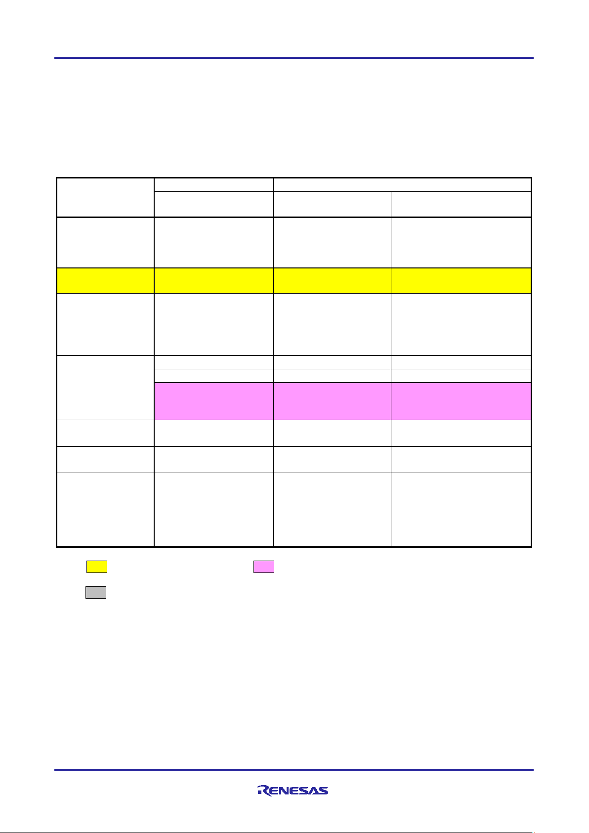
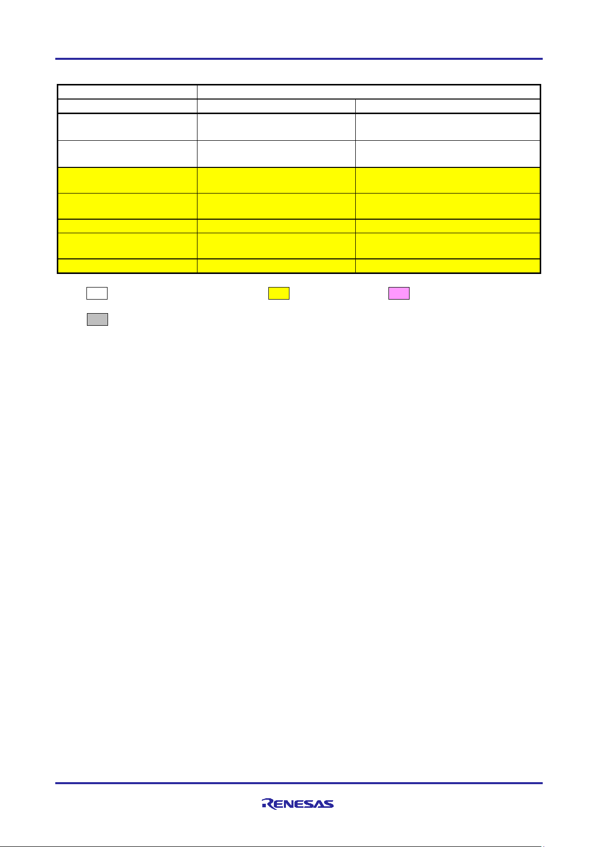
1. Differences in peripheral functions between RL78/G13 and RL78/G23
Table 1.1 and Table 1.3 show the main differences in peripheral functions between RL78/G13 and
RL78/G23.
However, differences due to changes in the settings of the CPU core, peripheral functions, and clock
generation circuit are not considered. For details, refer to the User's Manual: Hardware of each product.
Table 1.1 Differences in peripheral functions between RL78/G13 and RL78/G23 (1/3)
Item
Ports Port Functions Port Functions - Added output current control
port.
- Enhanced low-level output
Flash operation mode
Timers
12-bit Interval Timer 32-bit Interval Timer Changed function
Output Controller
Watchdog Timers
A/D Converter A/D Converter A/D Converter - Added 12-bit resolution.
Watchdog Timer Watchdog Timer Changed overflow time.
-
Operation State Control Additional function
oscillator.
- Changed frequency (fIL) of lowspeed on-chip oscillator to
(Capable of measuring up to
Output Controller
- Capable of selecting Digital I/O
or analog input for each pin.
(This pin function selection
applies also to ANI0 to ANI15
Note : Additional peripheral functions : Changed peripheral functions
: Deleted peripheral functions -: There is no corresponding function.
Caution. For details on peripheral functions, usage and electrical characteristics, refer to the User's Manual:
Hardware.
R01AN5378EJ0100 Rev.1.00 Page 3 of 24
Apr.13.21
Page 4
RL78/G13, RL78/G23 Migration Guide from RL78/G13 to RL78/G23
RL78/G13
RL78/G23
Function name
Function name
Main differences from
RL78/G13
D/A Converter
D/A Converter
Additional function
Comparator
Comparator
Additional function
Clock Synchronous)
Serial Array Unit
Added UART loopback function
I2C bus interface
IICA
IICA
Added all address match function
Remote Control Signal
Receiver
Receiver (REMC)
Accumulator
Multiplier and
Deleted item
instructions.)
Functions
Access) Controller
Controller)
Table 1.2 Differences in peripheral functions between RL78/G13 and RL78/G23 (2/3)
Item
-
-
Serial Interface
(Clock Asynchronous,
Serial Array Unit
UARTA Additional function
(computing unit)
Data Transfer
linkage operation
between peripheral
functions without CPU
-
Divider/MultiplyAccumulator
DMA (Direct Memory
-
Remote Control Signal
-
DTC (Data Transfer
Logic and Event Link
Controller (ELCL)
Additional function
(Added multiply & accumulate
Changed function
Additional function
Note : Additional peripheral functions : Changed peripheral functions
: Deleted peripheral functions -: There is no corresponding function.
Caution. For details on peripheral functions, usage and electrical characteristics, refer to the User's Manual:
Hardware.
R01AN5378EJ0100 Rev.1.00 Page 4 of 24
Apr.13.21
Page 5
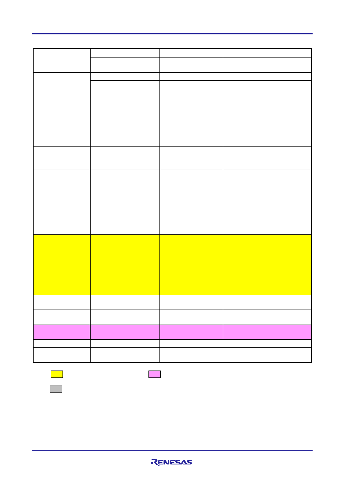
RL78/G13, RL78/G23 Migration Guide from RL78/G13 to RL78/G23
RL78/G13
RL78/G23
Function name
Function name
Main differences from
RL78/G13
Interrupts
Interrupt Functions
Interrupt Functions
Changed interrupt sources.
detection edge.
supply to RAM.
power-on reset has occurred.
Power-On-Reset Circuit
Power-On-Reset Circuit
Changed reset processing time.
values.
- Added UART loopback function.
encryption function
Processing execution
of CPU
SNOOZE Mode
Additional function
sensor
internal regulator.
Select Areas
and Flash operating modes.
Flash Memory
Flash Memory
Flash Memory
Changed specifications, such as
block size.
On-Chip Debugging
On-Chip Debugging
On-Chip Debugging
Changed dedicated emulators.
Circuit
Table 1.3 Differences in peripheral functions between RL78/G13 and RL78/G23 (3/3)
Item
Key Interrupt Function Key Interrupt Function - Added a function to select key
Interrupt detection pins.
- Added a function to select
Reduced system
operating current
Resets Reset Function Reset Function Added a function to confirm that a
Voltage Detector
(LVD)
Safety Functions Safety Functions Safety Functions - Added a function to prevent Flash
Security function,
function independent
Capacitive
touch/proximity
Standby Function Standby Function - Added a function that starting of
high-speed on-chip oscillator is at
high speed.
- Added a function to stop power
Voltage Detector Voltage Detector - Equipped with 2 channels.
- Changed detection voltage
rewriting when CPU goes out of
control.
- Added a function to detect digital
output signal level for I/O pins.
-
-
-
Security Function Additional function
Sequencer
Capacitive Sensing Unit Additional function
Regulator Regulator Regulator Changed an output voltage value of
Option Function
BCD Correction
Note : Additional peripheral functions : Changed peripheral functions
: Deleted peripheral functions -: There is no corresponding function.
Caution. For details on peripheral functions, usage and electrical characteristics, refer to the User's Manual:
Hardware.
R01AN5378EJ0100 Rev.1.00 Page 5 of 24
Apr.13.21
Option Bytes Option Bytes Changed functions of WDT, LVD,
BCD Correction Circuit BCD Correction Circuit None
Page 6
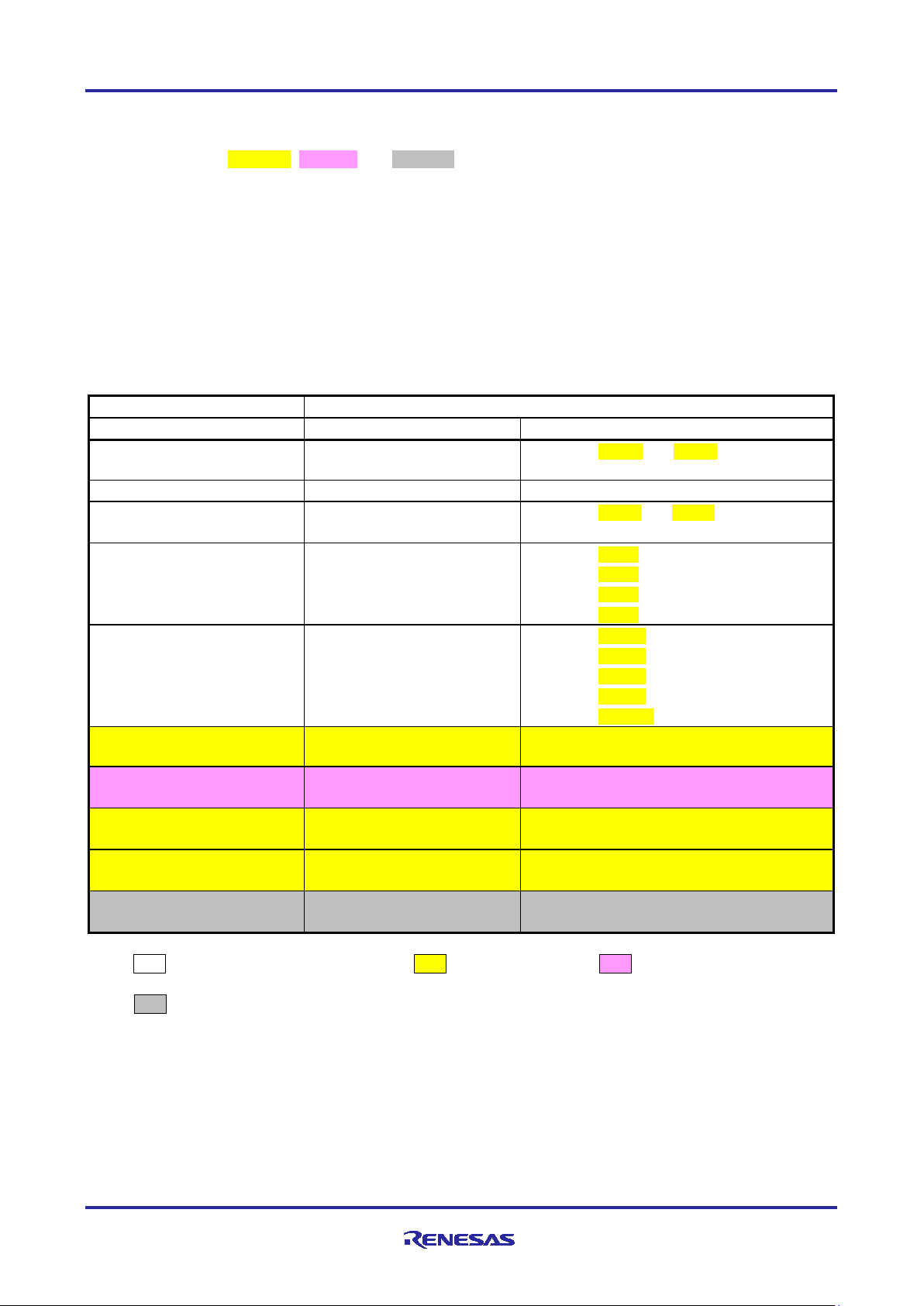
RL78/G13, RL78/G23 Migration Guide from RL78/G13 to RL78/G23
RL78/G13
RL78/G23
Register name
Register name
Remark
register
Port registers (Pxx)
Port registers (Pxx)
None
(PUxx)
Addition of PIM84 bit to PIM8 register.
Addition of POM120 bit to POM12 register.
Port digital input disable
registers (PDIDISxx)
New addition
(PMCxx)
(PMCAxx)
(PMCTxx)
(PMCExx)
A/D port configuration register
(ADPC)
Deleted item
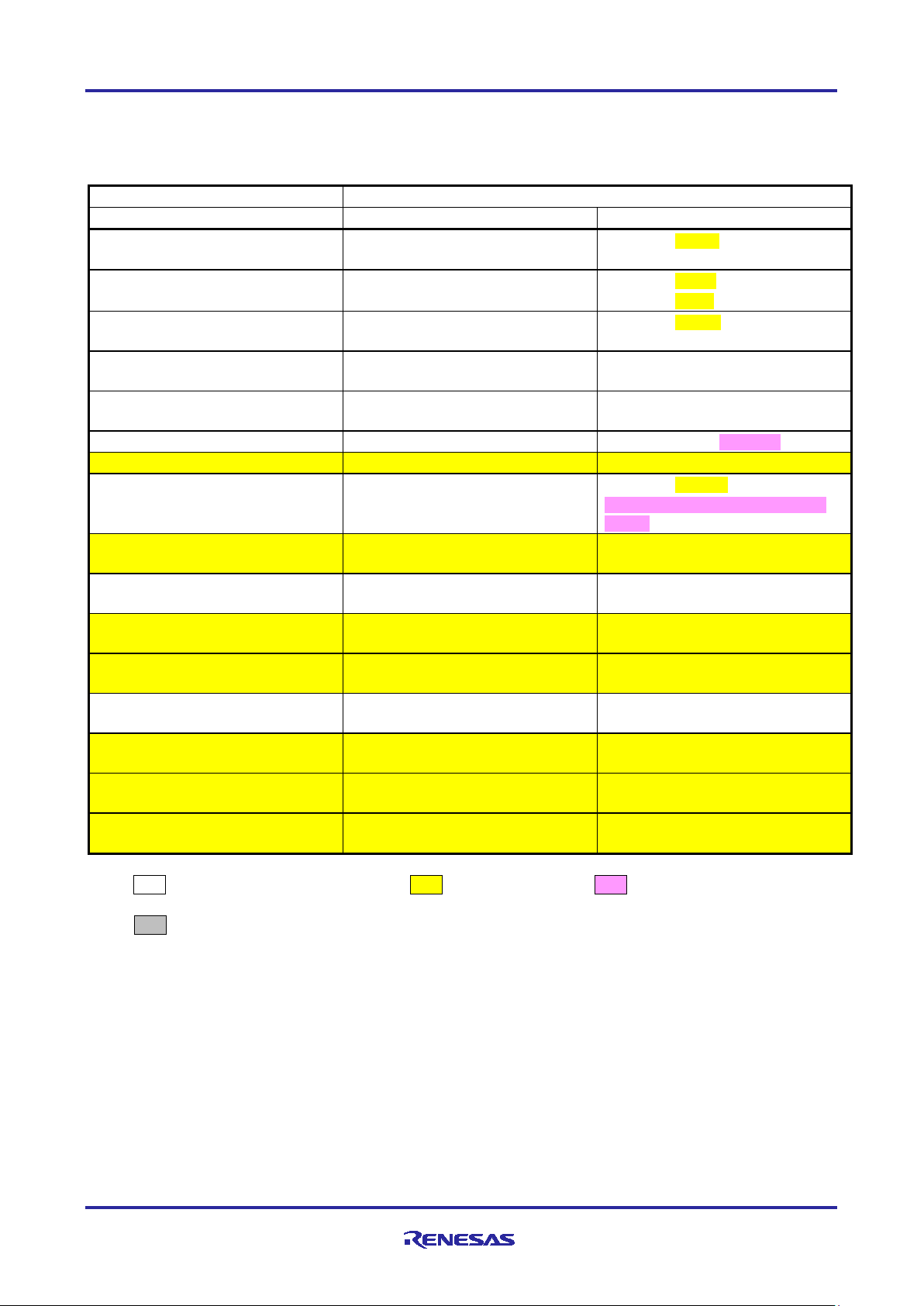
2. Comparison of RL78/G13 and RL78/G23 registers
Table 2.1 to Table 2.19 show register comparison between RL78/G13 and RL78/G23 for peripheral
functions other than additions, changes and deletions described in chapter "1. Differences in peripheral
functions between RL78/G13 and RL78/G23". For details of each register function, refer to the User's
Manual: Hardware.
Also, the registers and bits mounted on the microcontroller differ depending on the product. For the
registers and bits mounted in each product, refer to the User's Manual: Hardware.
2.1 Port Functions
Table 2.1 Registers Controlling Port Function (1/2)
Port mode registers (PMxx) Port mode registers (PMxx) Addition of PM121 and PM122 bits to PM12
Pull-up resistor option registers
(PUxx)
Port input mode registers
(PIMx)
Port output mode registers
(POMx)
-
Port mode control registers
-
-
Pull-up resistor option registers
Port input mode registers
(PIMxx)
Port output mode registers
(POMxx)
Port mode control A registers
Port mode control T registers
Port mode control E registers
-
Addition of PU121 and PU122 bits to PU12
register
Addition of PIM33 bit to PIM3 register.
Addition of PIM41 bit to PIM4 register.
Addition of PIM71 bit to PIM7 register.
Addition of POM34 bit to POM3 register.
Addition of POM42 bit to POM4 register.
Addition of POM72 bit to POM7 register.
Addition of POM83 bit to POM8 register.
Changed applicable pins
New addition
New addition
Note : The register name is unchanged. : Additional contents : Changed contents
: Deleted contents -: There is no corresponding register.
Caution. For details of each register function, refer to the User's Manual: Hardware.
R01AN5378EJ0100 Rev.1.00 Page 6 of 24
Apr.13.21
Page 7
RL78/G13, RL78/G23 Migration Guide from RL78/G13 to RL78/G23
RL78/G13
RL78/G23
Register name
Register name
Remark
register (PIOR)
Global digital input disable
Global digital input disable
register (GDIDIS)
None
register (CCDE)
(CCSx)
Port overdrive register (PTDC)
New addition
Port function output enable registers
(PFOEx)
New addition
Port mode select register (PMS)
New addition
Table 2.2 Registers Controlling Port Function (2/2)
Peripheral I/O redirection
register (PIOR)
register (GDIDIS)
-
-
-
-
-
Peripheral I/O redirection
Output current control enable
Output current select registers
None
New addition
New addition
Note : The register name is unchanged. : Additional contents : Changed contents
: Deleted contents -: There is no corresponding register.
Caution. For details of each register function, refer to the User's Manual: Hardware.
R01AN5378EJ0100 Rev.1.00 Page 7 of 24
Apr.13.21
Page 8
RL78/G13, RL78/G23 Migration Guide from RL78/G13 to RL78/G23
RL78/G13
RL78/G23
Register name
Register name
Remark
(CMC)
(CMC)
Addition of MCS1 bit to bit 1.
Clock operation status control register
(CSC)
Clock operation status control register
(CSC)
Addition of MIOEN bit to bit 1
status register (OSTC)
status register (OSTC)
register (OSTS)
register (OSTS)
Peripheral enable register 0 (PER0)
Peripheral enable register 0 (PER0)
Change of bit 7 to RTCWEN bit
Peripheral enable register 1 (PER1)
New addition
values.
(CKSEL)
frequency select register (HOCODIV)
frequency select register (HOCODIV)
Middle-speed on-chip oscillator
frequency select register (MOCODIV)
New addition
register (MOSCDIV)
register (HIOTRM)
register (HIOTRM)
trimming register (MIOTRM)
Low-speed on-chip oscillator trimming
register (LIOTRM)
New addition
(WKUPMD)
2.2 Clock Generator
Table 2.3 Registers Controlling Clock Generator
Clock operation mode control register
System clock control register (CKC) System clock control register (CKC) Addition of MCM1 bit to bit 0.
Oscillation stabilization time counter
Oscillation stabilization time select
-
Subsystem clock supply mode control
register (OSMC)
-
High-speed on-chip oscillator
-
-
Clock operation mode control register
Oscillation stabilization time counter
Oscillation stabilization time select
Subsystem clock supply mode control
register (OSMC)
Subsystem clock select register
High-speed on-chip oscillator
High-speed system clock division
Addition of XTSEL bit to bit 3
None
None
Addition of HIPREC bit to bit 0.
Change of bits 1 and 2 to undefined
New addition
None
New addition
High-speed on-chip oscillator trimming
-
-
-
High-speed on-chip oscillator trimming
Middle-speed on-chip oscillator
Standby mode release setting register
None
New addition
New addition
Note : The register name is unchanged : Additional contents : Changed contents
: Deleted contents -: There is no corresponding register.
Caution. For details of each register function, refer to the User's Manual: Hardware.
R01AN5378EJ0100 Rev.1.00 Page 8 of 24
Apr.13.21
Page 9

RL78/G13, RL78/G23 Migration Guide from RL78/G13 to RL78/G23
RL78/G13
RL78/G23
Register name
Register name
Remark
to RTCWEN bit.
(PRR0)
Timer clock select register m (TPSm)
Timer clock select register m (TPSm)
None
Timer mode register mn (TMRmn)
Timer mode register mn (TMRmn)
None
Timer status register mn (TSRmn)
Timer status register mn (TSRmn)
None
register m (TEm)
register m (TEm)
Timer channel start register m (TSm)
Timer channel start register m (TSm)
None
Timer channel stop register m (TTm)
Timer channel stop register m (TTm)
None
Timer input select register 0 (TIS0)
Timer input select register 0 (TIS0)
None
Timer input select register 1 (TIS1)
New addition
Timer output enable register m
(TOEm)
Timer output enable register m
(TOEm)
None
Timer output register m (TOm)
Timer output register m (TOm)
None
Timer output level register m (TOLm)
Timer output level register m (TOLm)
None
(TOMm)
(TOMm)
Input switch control register (ISC)
Input switch control register (ISC)
Addition of ISC2 to ISC7 bits to bits 2
to 7.
(NFEN1, NFEN2)
(NFEN1, NFEN2)
(PMCAxx)
(PMCTxx)
Port mode control E register
(PMCExx)
New addition
Port mode register (PMxx)
Port mode register (PMxx)
PM12 register.
Port register (Pxx)
Port register (Pxx)
None
Port function output enable
register 0 (PFOE0)
New addition
2.3 Timer Array Unit
Table 2.4 Registers Controlling Timer Array Unit
Peripheral enable register 0 (PER0) Peripheral enable register 0 (PER0) No change for bits 0 and 1 (TAU0EN,
TAU1EN) used to set this peripheral
function. However, bit 7 is changed
-
Timer channel enable status
-
Timer output mode register m
Noise filter enable registers 1, 2
Port mode control register (PMCxx) Port mode control A register
Peripheral reset control register 0
Timer channel enable status
Timer output mode register m
Noise filter enable registers 1, 2
New addition
None
None
None
Change of applicable pins
-
-
-
Port mode control T register
New addition
Addition of PM121 and PM122 bits to
Note : The register name is unchanged. : Additional contents : Changed contents
: Deleted contents -: There is no corresponding register.
Caution. For details of each register function, refer to the User's Manual: Hardware.
R01AN5378EJ0100 Rev.1.00 Page 9 of 24
Apr.13.21
Page 10

RL78/G13, RL78/G23 Migration Guide from RL78/G13 to RL78/G23
RL78/G13
RL78/G23
Register name
Register name
Remark
Peripheral enable register 0 (PER0)
Peripheral enable register 0 (PER0)
Bit 7 is changed to RTCWEN bit.
undefined values.
Realtime clock control register 0
(RTCC0)
Realtime clock control register 0
(RTCC0)
Addition of RTC128EN bit to bit 4
(RTCC1)
(RTCC1)
Second count register (SEC)
Second count register (SEC)
None
Minute count register (MIN)
Minute count register (MIN)
None
Hour count register (HOUR)
Hour count register (HOUR)
None
Day count register (DAY)
Day count register (DAY)
None
Day-of-week count register (WEEK)
Day-of-week count register (WEEK)
None
Month count register (MONTH)
Month count register (MONTH)
None
Year count register (YEAR)
Year count register (YEAR)
None
(SUBCUD)
(SUBCUD)
Alarm minute register (ALARMWM)
Alarm minute register (ALARMWM)
None
Alarm hour register (ALARMWH)
Alarm hour register (ALARMWH)
None
Alarm day-of-week register
(ALARMWW)
Alarm day-of-week register
(ALARMWW)
None
added to bits 2 to 7.
Port register 3 (P3)
Port register 3 (P3)
None
2.4 Realtime Clock
Table 2.5 Registers Controlling the Realtime Clock
Subsystem clock supply mode
control register (OSMC)
Realtime clock control register 1
Time error correction register
Port mode register 3 (PM3) Port mode register 3 (PM3) No change for bit 0 (PM30) used to
Subsystem clock supply mode
control register (OSMC)
Realtime clock control register 1
Time error correction register
No change for bit 4 (WUTMMCK0)
used to set this peripheral function.
However, HIPREC bit is added to bit
0. Bits 1 and 2 are changed to
None
None
set this peripheral function.
However, PM32 to PM37 bits are
Note : The register name is unchanged. : Additional contents : Changed contents
: Deleted contents -: There is no corresponding register.
Caution. For details of each register function, refer to the User's Manual: Hardware.
R01AN5378EJ0100 Rev.1.00 Page 10 of 24
Apr.13.21
Page 11

RL78/G13, RL78/G23 Migration Guide from RL78/G13 to RL78/G23
RL78/G13
RL78/G23
Register name
Register name
Remark
(CKSn)
(CKSn)
(PM1, PM3, PM5, PM14)
(PM1, PM3, PM5, PM14)
Port registers 1, 3, 5, 14
(P1, P3, P5, P14)
Port registers 1, 3, 5, 14
(P1, P3, P5, P14)
None
(PMCTxx)
(PMCExx)
RL78/G13
RL78/G23
Register name
Register name
Remark
(WDTE)
(WDTE)
2.5 Clock Output/Buzzer Output Controller
Table 2.6 Registers Controlling Clock Output/Buzzer Output Controller
Clock output select registers n
Port mode registers
1, 3, 5, 14
-
-
Clock output select registers n
Port mode registers
1, 3, 5, 14
Port mode control T registers
Port mode control E registers
None
None
New addition
New addition
Note : The register name is unchanged. : Additional contents : Changed contents
: Deleted contents -: There is no corresponding register.
Caution. For details of each register function, refer to the User's Manual: Hardware.
2.6 Watchdog Timer
Table 2.7 Register Controlling Watchdog Timer
Watchdog timer enable register
Watchdog timer enable register
None
Note : The register name is unchanged. : Additional contents : Changed contents
: Deleted contents -: There is no corresponding register.
Caution. For details of each register function, refer to the User's Manual: Hardware.
R01AN5378EJ0100 Rev.1.00 Page 11 of 24
Apr.13.21
Page 12

RL78/G13, RL78/G23 Migration Guide from RL78/G13 to RL78/G23
RL78/G13
RL78/G23
Register name
Register name
Remark
bit 5 (ADCEN) used to set
is changed to RTCWEN bit.
(PRR0)
A/D converter mode register 0
(ADM0)
A/D converter mode register 0
(ADM0)
None
Addition of ADLSP bit to bit 3.
Addition of ADTYP1 bit to bit 1.
conversion.
8-bit A/D conversion result register
(ADCRH)
8-bit A/D conversion result register
(ADCRnH)
Changed applicable pins
register (ADS)
register (ADS)
limit setting register (ADUL)
upper limit setting register (ADUL)
limit setting register (ADLL)
lower limit setting register (ADLL)
A/D test register (ADTES)
A/D test register (ADTES)
None
(ADPC)
PMC12, PMC14)
PMCA11, PMCA12, PMCA14)
(PMCT0, PMCT3)
Port mode control E registers 0, 3
(PMCE0, PMCE3)
New addition
PM12, PM14, PM15)
PM12, PM14, PM15)
2.7 A/D Converter
Table 2.8 Registers Controlling A/D Converter
Peripheral enable register 0 (PER0) Peripheral enable register 0
(PER0)
-
A/D converter mode register 1
(ADM1)
A/D converter mode register 2
(ADM2)
10-bit A/D conversion result register
(ADCR)
Analog input channel specification
Conversion result comparison upper
Conversion result comparison lower
Peripheral reset control register 0
A/D converter mode register 1
(ADM1)
A/D converter mode register 2
(ADM2)
12-bit/10-bit A/D conversion result
register (ADCRn)
Analog input channel specification
Conversion result comparison
Conversion result comparison
No change for
this peripheral function. However, bit 7
New addition
Addition of ADTRS2 bit to bit 2.
Bit 0 is changed to ADTYP0 bit.
- Changed the register name.
- Added 12-bit resolution A/D
None
None
None
A/D port configuration register
Port mode control registers
0, 3, 10, 11, 12, and 14
(PMC0, PMC3, PMC10, PMC11,
-
-
Port mode registers
0, 2, 3, 10, 11, 12, 14, and 15
(PM0, PM2, PM3, PM10, PM11,
-
Port mode control A registers
0, 3, 10, 11, 12, and 14
(PMCA0, PMCA3, PMCA10,
Port mode control T registers 0, 3
Port mode registers
0, 2, 3, 10, 11, 12, 14, and 15
(PM0, PM2, PM3, PM10, PM11,
Deleted item.
Changed applicable pins
New addition
Addition of PM121 and PM122 bits to
PM12 register.
Note : The register name is unchanged. : Additional contents : Changed contents
: Deleted contents -: There is no corresponding register.
Caution. For details of each register function, refer to the User's Manual: Hardware.
R01AN5378EJ0100 Rev.1.00 Page 12 of 24
Apr.13.21
Page 13

RL78/G13, RL78/G23 Migration Guide from RL78/G13 to RL78/G23
RL78/G13
RL78/G23
Register name
Register name
Remark
RTCWEN bit.
(PRR0)
Serial clock select register m (SPSm)
Serial clock select register m (SPSm)
None
Serial mode register mn (SMRmn)
Serial mode register mn (SMRmn)
None
setting register mn (SCRmn)
setting register mn (SCRmn)
Serial data register mn (SDRmn)
Serial data register mn (SDRmn)
None
Serial flag clear trigger register mn
(SIRmn)
Serial flag clear trigger register mn
(SIRmn)
None
Serial status register mn (SSRmn)
Serial status register mn (SSRmn)
None
Serial channel start register m (SSm)
Serial channel start register m (SSm)
None
Serial channel stop register m (STm)
Serial channel stop register m (STm)
None
Serial channel enable status
register m (SEm)
Serial channel enable status
register m (SEm)
None
(SOEm)
(SOEm)
Serial output level register m (SOLm)
Serial output level register m (SOLm)
None
Serial output register m (SOm)
Serial output register m (SOm)
None
Serial standby control
register m (SSCm)
Serial standby control
register m (SSCm)
None
to 7.
Noise filter enable register 0 (NFEN0)
Noise filter enable register 0 (NFEN0)
None
2.8 Serial Array Unit
Table 2.9 Registers Controlling Serial Array Unit (1/2)
Peripheral enable register 0 (PER0) Peripheral enable register 0 (PER0) No change for bits 2 and 3 (SAU0EN,
SAU1EN) used to set this peripheral
function. However, bit 7 is changed to
-
Serial communication operation
Serial output enable register m
Input switch control register (ISC) Input switch control register (ISC) Addition of ISC2 to ISC7 bits to bits 2
Peripheral reset control register 0
Serial communication operation
Serial output enable register m
New addition
None
None
Note : The register name is unchanged. : Additional contents : Changed contents
: Deleted contents -: There is no corresponding register.
Caution. For details of each register function, refer to the User's Manual: Hardware.
R01AN5378EJ0100 Rev.1.00 Page 13 of 24
Apr.13.21
Page 14

RL78/G13, RL78/G23 Migration Guide from RL78/G13 to RL78/G23
RL78/G13
RL78/G23
Register name
Register name
Remark
PIM14)
PIM14)
Port output mode registers
Port output mode registers
Addition of POM42 bit to POM4
register.
(PMC0, PMC3, PMC14)
(PMCA0, PMCA3, PMCA14)
(PMCT0, PMCT3)
(PMCE0)
Port function output enable registers
(PFOEx)
New addition
PM9, PM14)
PM9, PM14)
(P0, P1, P3 to P5, P7 to P9, P14)
(ULBS)
Table 2.10 Registers Controlling Serial Array Unit (2/2)
Port input mode registers
0, 1, 4, 5, 8, 14
(PIM0, PIM1, PIM4, PIM5, PIM8,
0, 1, 4, 5, 7 to 9, 14
(POM0, POM1, POM4, POM5,
POM7 to POM9, POM14)
Port mode control registers 0, 3, 14
-
-
-
Port mode registers
0, 1, 3 to 5, 7 to 9, 14
(PM0, PM1, PM3 to PM5, PM7 to
Port registers 0, 1, 3 to 5, 7 to 9, 14
-
Port input mode registers
0, 1, 4, 5, 8, 14
(PIM0, PIM1, PIM4, PIM5, PIM8,
0, 1, 4, 5, 7 to 9, 14
(POM0, POM1, POM4, POM5,
POM7 to POM9, POM14)
Port mode control A registers 0, 3, 14
Port mode control T registers 0, 3
Port mode control E register 0
Port mode registers
0, 1, 3 to 5, 7 to 9, 14
(PM0, PM1, PM3 to PM5, PM7 to
Port registers 0, 1, 3 to 5, 7 to 9, 14
(P0, P1, P3 to P5, P7 to P9, P14)
UART loopback select register
Addition of PIM41 bit to PIM4
register.
Addition of PIM84 bit to PIM8
register.
register.
Addition of POM72 bit to POM7
register.
Addition of POM83 bit to POM8
Changed applicable pins
New addition
New addition
None
None
New addition
Note : The register name is unchanged. : Additional contents : Changed contents
: Deleted contents -: There is no corresponding register.
Caution. For details of each register function, refer to the User's Manual: Hardware.
R01AN5378EJ0100 Rev.1.00 Page 14 of 24
Apr.13.21
Page 15

RL78/G13, RL78/G23 Migration Guide from RL78/G13 to RL78/G23
RL78/G13
RL78/G23
Register name
Register name
Remark
RTCWEN bit.
(PRR0)
IICA control register n0 (IICCTLn0)
IICA control register n0 (IICCTLn0)
None
IICA status register n (IICSn)
IICA status register n (IICSn)
None
IICA flag register n (IICFn)
IICA flag register n (IICFn)
None
IICA control register n1 (IICCTLn1)
IICA control register n1 (IICCTLn1)
Addition of SVADISn bit to bit 6.
IICA low-level width setting register n
(IICWLn)
IICA low-level width setting register n
(IICWLn)
None
register n (IICWHn)
register n (IICWHn)
Port mode register 6 (PM6)
Port mode register 6 (PM6)
None
Port register 6 (P6)
Port register 6 (P6)
None
2.9 Serial Interface IICA
Table 2.11 Registers Controlling Serial Interface IICA
Peripheral enable register 0 (PER0) Peripheral enable register 0 (PER0) No change for bits 6 and 4 (IICA1EN,
IICA0EN) used to set this peripheral
function. However, bit 7 is changed to
-
IICA high-level width setting
Peripheral reset control register 0
IICA high-level width setting
New addition
None
Note : The register name is unchanged. : Additional contents : Changed contents
: Deleted contents -: There is no corresponding register.
Caution. For details of each register function, refer to the User's Manual: Hardware.
R01AN5378EJ0100 Rev.1.00 Page 15 of 24
Apr.13.21
Page 16

RL78/G13, RL78/G23 Migration Guide from RL78/G13 to RL78/G23
RL78/G13
RL78/G23
Register name
Register name
Remark
Interrupt request flag registers
Interrupt request flag registers
Addition of IF3H register.
IF3L.
Interrupt mask flag registers
Interrupt mask flag registers
Addition of MK3H register.
MK2H and MK3L.
Priority specification flag
Priority specification flag
PR13H)
Addition of PR03H and PR13H.
External interrupt rising edge
enable registers (EGP0, EGP1)
External interrupt rising edge
enable registers (EGP0, EGP1)
None
External interrupt falling edge
enable registers (EGN0, EGN1)
External interrupt falling edge
enable registers (EGN0, EGN1)
None
Program status word (PSW)
Program status word (PSW)
None
2.10 Interrupt Functions
Table 2.12 Registers Controlling Interrupt Functions
(IF0L, IF0H, IF1L, IF1H,
IF2L, IF2H, IF3L)
(MK0L, MK0H, MK1L, MK1H,
MK2L, MK2H, MK3L)
registers
(PR00L, PR00H, PR01L,
PR01H, PR02L, PR02H,
PR03L, PR10L, PR10H,
PR11L, PR11H, PR12L,
PR12H, PR13L)
Note : The register name is unchanged. : Additional contents : Changed contents
: Deleted contents -: There is no corresponding register.
Caution. For details of each register function, refer to the User's Manual: Hardware.
(IF0L, IF0H, IF1L, IF1H,
IF2L, IF2H, IF3L, IF3H)
(MK0L, MK0H, MK1L, MK1H,
MK2L, MK2H, MK3L, MK3H)
registers
(PR00L, PR00H, PR01L,
PR01H, PR02L, PR02H,
PR03L, PR03H, PR10L,
PR10H, PR11L, PR11H,
PR12L, PR12H, PR13L,
Change of the contents of IF0H,
IF1L, IF1H (ITIF → ITLIF bit),
IF2L (PIF10 → FLIF bit), IF2H and
Change of the contents of MK0H,
MK1L, MK1H (ITMK → ITLMK bit),
MK2L (PMK10 → FLMK bit),
Change of the contents of PR00H,
PR10H, PR01L, PR11L, PR01H,
PR11H (ITPR0, ITPR1 → ITLPR0,
ITLPR1 bit), PR02L, PR12L
(PPR010, PPR110
FLPR1 bit), PR02H, PR12H,
PR03L and PR13L.
→ FLPR0,
R01AN5378EJ0100 Rev.1.00 Page 16 of 24
Apr.13.21
Page 17

RL78/G13, RL78/G23 Migration Guide from RL78/G13 to RL78/G23
RL78/G13
RL78/G23
Register name
Register name
Remark
Key return control register
(KRCTL)
New addition
Key return mode register (KRM)
Key return mode register 0
(KRM0)
Key return flag register (KRF)
New addition
Port mode register 7 (PM7)
Port mode register 7 (PM7)
None
RL78/G13
RL78/G23
Register name
Register name
Remark
Subsystem clock supply mode
Subsystem clock supply mode
undefined values.
Oscillation stabilization time
counter status register (OSTC)
Oscillation stabilization time
counter status register (OSTC)
None
Oscillation stabilization time
select register (OSTS)
Oscillation stabilization time
select register (OSTS)
None
Standby mode release setting
register (WKUPMD)
New addition
Memory power reduction control
register (PSMCR)
New addition
2.11 Key Interrupt Function
Table 2.13 Register Controlling the Key Interrupt
-
Changed applicable pins
-
Note : The register name is unchanged. : Additional contents : Changed contents
: Deleted contents -: There is no corresponding register.
Caution. For details of each register function, refer to the User's Manual: Hardware.
2.12 Standby Function
Table 2.14 Registers Controlling Standby Function
Addition of HIPREC bit to bit 0.
control register (OSMC)
-
-
Note : The register name is unchanged. : Additional contents : Changed contents
: Deleted contents -: There is no corresponding register.
Caution. For details of each register function, refer to the User's Manual: Hardware.
control register (OSMC)
Bits 1 and 2 are changed to
R01AN5378EJ0100 Rev.1.00 Page 17 of 24
Apr.13.21
Page 18

RL78/G13, RL78/G23 Migration Guide from RL78/G13 to RL78/G23
RL78/G13
RL78/G23
Register name
Register name
Remark
Reset control flag register (RESF)
Reset control flag register (RESF)
None
Power-on-reset status register
(PORSR)
New addition
Peripheral reset control register 0
(PRR0)
New addition
Peripheral reset control register 1
(PRR1)
New addition
2.13 Reset Function
Table 2.15 Registers for Confirming Reset Sources
-
-
-
Note : The register name is unchanged. : Additional contents : Changed contents
: Deleted contents -: There is no corresponding register.
Caution. For details of each register function, refer to the User's Manual: Hardware.
2.14 Power-On-Reset Circuit
There is no register that controls the power-on-reset circuit.
R01AN5378EJ0100 Rev.1.00 Page 18 of 24
Apr.13.21
Page 19

RL78/G13, RL78/G23 Migration Guide from RL78/G13 to RL78/G23
RL78/G13
RL78/G23
Register name
Register name
Remark
User option byte
(Settings related to LVD.)
User option byte
(Settings related to LVD.)
Changed functions of option bytes.
Voltage detection register
Voltage detection register
Bit 3 has been changed to DLVD1F bit.
LVD detection flag clearing
register (LVDFCLR)
New addition
Voltage detection level register
Voltage detection level register
Bit 7 is changed to LVD1EN bit.
2.15 Voltage Detector
Table 2.16 Registers Controlling Voltage Detector
000C1H/010C1H
000C1H/040C1H
Changed address when using the
boot swap operation.
Bit 0 has been changed to LVD0F bit.
(LVIM)
-
(LVIS)
(LVIM)
(LVIS)
Bit 1 has been changed to LVD1F bit.
Bit 2 has been changed to DLVD0F bit.
Bit 0 is changed to LVD1V0 bit.
Bit 1 is changed to LVD1V1 bit.
Bit 2 is changed to LVD1V2 bit.
Bit 3 is changed to LVD1V3 bit.
Bit 4 is changed to LVD1V4 bit.
Bit 6 is changed to LVD1SEL bit.
Note : The register name is unchanged : Additional contents : Changed contents
: Deleted contents -: There is no corresponding register.
Caution. For details of each register function, refer to the User's Manual: Hardware.
R01AN5378EJ0100 Rev.1.00 Page 19 of 24
Apr.13.21
Page 20

RL78/G13, RL78/G23 Migration Guide from RL78/G13 to RL78/G23
RL78/G13
RL78/G23
Register name
Register name
Remark
Flash memory CRC control
register (CRC0CTL)
Flash memory CRC control
register (CRC0CTL)
None
Flash memory CRC operation
result register (PGCRCL)
Flash memory CRC operation
result register (PGCRCL)
None
CRC input register (CRCIN)
CRC input register (CRCIN)
None
CRC data register (CRCD)
CRC data register (CRCD)
None
Code flash memory guard
register (GFLASH0)
New addition
Data flash memory guard
register (GFLASH1)
New addition
Flash security area guard
register (GFLASH2)
New addition
RAM parity error control register
(RPECTL)
RAM parity error control register
(RPECTL)
None
Invalid memory access detection
control register (IAWCTL)
Invalid memory access detection
control register (IAWCTL)
None
Guard register of IAWCTL
register (GIAWCTL)
New addition
Timer input select register 0
(TIS0)
Timer input select register 0
(TIS0)
None
A/D test register (ADTES)
A/D test register (ADTES)
None
Analog input channel
specification register (ADS)
Analog input channel
specification register (ADS)
None
Port mode select register (PMS)
New addition
UART loopback select register
(ULBS)
New addition
2.16 Safety Functions
Table 2.17 Registers Used by Safety Functions
-
-
-
-
-
-
Note : The register name is unchanged. : Additional contents : Changed contents
: Deleted contents -: There is no corresponding register.
Caution. For details of each register function, refer to the User's Manual: Hardware.
2.17 Regulator
There is no register that controls the regulator.
R01AN5378EJ0100 Rev.1.00 Page 20 of 24
Apr.13.21
Page 21

RL78/G13, RL78/G23 Migration Guide from RL78/G13 to RL78/G23
RL78/G13
RL78/G23
Option byte area
Option byte area
Remark
000C0H-000C3H
000C0H-000C3H
Changed functions of option bytes.
User option bytes
User option bytes
000C0H/010C0H
(Settings related to WDT.)
000C0H/040C0H
(Settings related to WDT.)
000C1H/010C1H
(Settings related to LVD.)
000C1H/040C1H
(Settings related to LVD.)
000C2H/010C2H
HOCO.)
000C2H/040C2H
HOCO.)
On-chip debug option byte
On-chip debug option byte
RL78/G13
RL78/G23
Register name
Register name
Remark
BCD correction result register
(BCDADJ)
BCD correction result register
(BCDADJ)
None
2.18 Option Bytes
There is no register that controls the option bytes. The function of option bytes is set using the option byte
area. Table 2.18 shows a comparison of RL78/G13 and RL78/G23 option byte areas.
Table 2.18 Option Byte Area
(Normal/Boot swap operation)
/010C0H-010C3H
000C0H-000C2H
/010C0H-010C2H
(Settings related to flash and
000C3H/010C3H
Note : The option bytes name is unchanged. : Additional contents : Changed contents
: Deleted contents -: There is no corresponding register.
Caution. For details of the function of each option bytes, refer to the User's Manual: Hardware.
(Normal/Boot swap operation)
/040C0H-040C3H
000C0H-000C2H
/040C0H-040C2H
(Settings related to flash and
000C3H/040C3H
Changed address when using the
boot swap operation.
2.19 On-Chip Debugging
There is no register that controls the on-chip debugging function.
2.20 BCD Correction Circuit
Note : The register name is unchanged. : Additional contents : Changed contents
: Deleted contents -: There is no corresponding register.
Caution. For details of each register function, refer to the User's Manual: Hardware.
Table 2.19 Register Used by BCD Correction Circuit
R01AN5378EJ0100 Rev.1.00 Page 21 of 24
Apr.13.21
Page 22

RL78/G13, RL78/G23 Migration Guide from RL78/G13 to RL78/G23
3. Other changes and notes
3.1 RL78/G23 instruction set
"Multiply and accumulation register (MACR)", which is used in the multiply and accumulation instructions, is
added on RL78/G23. (The MACR register is composed of multiply and accumulation register (H)/(L):
MACRH/MACRL).
R01AN5378EJ0100 Rev.1.00 Page 22 of 24
Apr.13.21
Page 23

RL78/G13, RL78/G23 Migration Guide from RL78/G13 to RL78/G23
4. Documents for Reference
RL78/G13 User's Manual: Hardware (R01UH0146)
RL78/G23 User's Manual: Hardware (R01UH0896)
RL78 Family User's Manual: Software (R01US0015)
(The latest versions of the documents are available on the Renesas Electronics Website.)
Technical Updates/Technical Brochures
(The latest versions of the documents are available on the Renesas Electronics Website.)
R01AN5378EJ0100 Rev.1.00 Page 23 of 24
Apr.13.21
Page 24

RL78/G13, RL78/G23 Migration Guide from RL78/G13 to RL78/G23
Rev.
Date
Description
Page
Summary
1.00
Apr.13.21
-
First edition issued
Revision History
R01AN5378EJ0100 Rev.1.00 Page 24 of 24
Apr.13.21
Page 25

General Precautions in the Handling of Microprocessing Unit and Microcontroller Unit Products
The following usage notes are applicable to all Microprocessing unit and Microcontroller unit products from Renesas. For detailed usage notes on the
products covered by this document, refer to the relevant sections of the document as well as any technical updates that have been issued for the products.
1. Precaution against Electrostatic Discharge (ESD)
A strong electrical field, when exposed to a CMOS device, can cause destruction of the gate oxide and ultimately degrade the device operation. Steps
must be taken to stop the generation of static electricity as much as possible, and quickly dissipate it when it occurs. Environmental control must be
adequate. When it is dry, a humidifier should be used. This is recommended to avoid using insulators that can easily build up static electricity.
Semiconductor devi ces must be stored and transported in an anti-static container, static shielding bag or conductive material. All test and
measurement tools including work benches and floors must be grounded. The operator must also be grounded using a wrist strap. Semiconductor
devices must not be touched with bare hands. Similar precautions must be taken for printed circuit boards with mounted semiconductor devices.
2. Processing at power-on
The state of the product is undefined at the time when power is supplied. The states of internal circuits in the LSI are indeterminate and the states of
register settings and pins are undefined at the time when power is supplied. In a finished product where the reset signal is applied to the external reset
pin, the states of pins are not guaranteed from the time when power is supplied until the reset process is completed. In a similar way, the states of pins
in a product that is reset by an on-chip power-on reset function are not guaranteed from the time when power is supplied until the power reaches the
level at which resetting is specified.
3. Input of signal during power-off state
Do not input signals or an I/O pull-up power supply while the device is powered off. The current injection that results from input of such a signal or I/O
pull-up power supply may cause malfunction and the abnormal current that passes in the device at this time may cause degradation of internal
elements. Follow the guideline for input signal during power-off state as described in your product documentation.
4. Handling of unused pins
Handle unused pins in accordance with the directions given under handling of unused pins in the manual. The input pins of CMOS products are
generally in the high-impedance state. In operation with an unused pi n in the open-circuit state, extra electromagnetic noise is induced in the vicinity of
the LSI, an associated shoot-through current flows internally, and malfunctions occur due to the false recognition of the pin state as an input signal
become possible.
5. Clock signals
After applying a reset, only release the reset line after the operating clock signal becomes stable. When switching the clock signal during program
execution, wait until the target clock signal is stabilized. When the clock signal is generated with an external resonator or from an external oscillator
during a reset, ensure that the reset line is only released after full stabilization of the clock signal. Additionally, when switching to a clock signal
produced with an external resonator or by an external oscillator while program execution is in progress, wait until the target clock signal is stable.
6. Voltage application waveform at input pin
Waveform distortion due to input noise or a reflected wave may cause malfunction. If the input of the CMOS device stays in the area between V
(Max.) and V
input level is fixed, and also in the transition period when the input level passes through the area between V
7. Prohibition of access to reserved addresses
Access to reserved addresses is prohibited. The reserved addresses are provided for possible future expansion of functions. Do not access these
addresses as the correct operation of the LSI is not guaranteed.
8. Differences between products
Before changing from one product to another, for example to a product with a different part number, confirm that the change will not lead to problems.
The characteristics of a microprocessing unit or microcontroller unit products in the same group but having a different part number might differ in terms
of internal memory capacity, layout pattern, and other factors, which can affect the ranges of electrical characteristics, such as characteristic values,
operating margins, immunity to noise, and amount of radiated noise. When changing to a product with a different part number, implement a system-
evaluation test for the given product.
(Min.) due to noise, for example, the device may malfunction. Take care to prevent chattering noise from entering the device when the
IH
(Max.) and VIH (Min.).
IL
IL
Page 26

Corporate Headquarters
Contact information
www.renesas.com
Trademarks
of their respective owners.
Notice
1. Descriptions of circuits, software and other related information in this document are provided only to illustrate the operation of semiconductor products
and application examples. You are fully responsible for the incorporation or any other use of the circuits, software, and information i n the design of your
product or system. Renesas Electronics disclaims any and all liability for any losses and damages incurred by you or third parties arising from the use
of these circuits, software, or information.
2. Renesas Electronics hereby expressly disclaims any warranties against and liability for infringement or any other claims involving patents, copyrights,
or other intellectual property rights of third parties, by or arising from the use of Renesas Electronics products or technical information described in this
document, including but not limited to, the product data, drawings, charts, programs, algorithms, and application examples.
3. No license, express, implied or otherwise, is granted hereby under any patents, copyrights or other intellectual property rights of Renesas Electronics
or others.
4. You shall be responsible for determining what licenses are required from any third parties, and obtaining such licenses for the lawful import, export,
manufacture, sales, utilization, distribution or other disposal of any products incorporating Renesas Electronics products, if required.
5. You shall not alter, modify, copy, or reverse engineer any Renesas Electronics product, whether in whole or i n part. Renesas Electronics disclaims any
and all liability for any losses or damages incurred by you or third parties arising from such alteration, modification, copying or reverse engineering.
6. Renesas Electronics products are classified according to the following two quality grades: “Standard” and “High Quality”. The intended applications for
each Renesas Electronics product depends on the product’s quality grade, as indicated below.
"Standard": Computers; office equipment; communications equipment; test and measurement equipment; audio and visual equipment; home
"High Quality": Transportation equipment (automobiles, trains, ships, etc.); traffic control (traffic lights); large-scale communication equipment; key
Unless expressly designated as a high reliability product or a product for harsh environments in a Renesas Electronics data sheet or other Renesas
Electronics document, Renesas Electronics products are not intended or authorized for use in products or systems that may pose a direct threat to
human life or bodily injury (artificial life support devices or systems; surgical implantations; etc.), or may cause serious property damage (space
system; undersea repeaters; nuclear power control systems; aircraft control systems; key plant systems; military equipment; etc.). Renesas Electronics
disclaims any and all liability for any damages or losses incurred by you or any third parties arising from the use of any Renesas Electronics product
that is inconsistent with any Renesas Electronics data sheet, user’s manual or other Renesas Electronics document.
7. No semiconductor product is absolutely secure. Notwithstanding any security measures or features that may be implemented in Renesas Electronics
hardware or software products, Renesas Electronics shall have absolutely no liability arising out of any vulnerability or security breach, including but
not limited to any unauthorized access to or use of a Renesas Electronics product or a system that uses a Renesas Electronics product. RENESAS
ELECTRONICS DOES NOT WARRANT OR GUARANTEE THAT RENESAS ELECTRONICS PRODUCTS, OR ANY SYSTEMS CREATED USING
RENESAS ELECTRONICS PRODUCTS WILL BE INVULNERABLE OR FREE FROM CORRUPTION, ATTACK, VIRUSES, INTERFERENCE,
HACKING, DATA LOSS OR THEFT, OR OTHER SECURITY INTRUSION (“Vulnerability Issues”). RENESAS ELECTRONICS DISCLAIMS ANY AND
ALL RESPONSIBILITY OR LIABILITY ARISING FROM OR RELATED TO ANY VULNERABILITY ISSUES. FURTHERMORE, TO THE EXTENT
PERMITTED BY APPLICABLE LAW, RENESAS ELECTRONICS DISCLAIMS ANY AND ALL WARRANTIES, EXPRESS OR IMPLIED, WITH
RESPECT TO THIS DOCUMENT AND ANY RELATED OR ACCOMPANYING SOFTWARE OR HARDWARE, INCLUDING BUT NOT LIMITED TO
THE IMPLIED WARRANTIES OF MERCHANTABILITY, OR FITNESS FOR A PARTICULAR PURPOSE.
8. When using Renesas Electronics products, refer to the latest product information (data sheets, user’s manuals, application notes, “General Notes for
Handling and Using Semiconductor Devices” in the reliability handbook, etc.), and ensure that usage conditions are within the ranges specified by
Renesas Electronics with respect to maximum ratings, operating power supply voltage range, heat dissipation characteristics, installation, etc. Renesas
Electronics disclaims any and all liability for any malfunctions, failure or accident arising out of the use of Renesas Electronics products outside of such
specified ranges.
9. Although Renesas Electronics endeavors to improve the quality and reliability of Renesas Electronics products, semiconductor products have specific
characteristics, such as the occurrence of failure at a certain rate and malfunctions under certain use conditions. Unless designated as a high reliability
product or a product for harsh environments in a Renesas Electronics data sheet or other Renesas Electronics document, Renesas Electronics
products are not subject to radiation resistance design. You are responsible for implementing safety measures to guard against the possibility of bodily
injury, injury or damage caused by fire, and/or danger to the public in the event of a failure or malfunction of Renesas Electronics products, such as
safety design for hardware and software, including but not limited to redundancy, fire control and malfunction prevention, appropriate treatment for
aging degradation or any other appropriate measures. Because the evaluation of microcomputer software alone is very difficult and impractical, you are
responsible for evaluating the safety of the final products or systems manufactured by you.
10. Please contact a Renesas Electronics sales office for details as to environmental matters such as the environmental compatibility of each Renesas
Electronics product. You are responsible for carefully and sufficiently investigating applicable laws and regulations that regulate the inclusion or use of
controlled substances, including without limitation, the EU RoHS Directive, and using Renesas Electronics products in compliance with all these
applicable laws and regulations. Renesas Electronics disclaims any and all liability for damages or losses occurring as a result of your noncompliance
with applicable law s and regulations.
11. Renesas Electronics products and technologies shall not be used for or incorporated into any products or systems whose manufacture, use, or sale is
prohibited under any applicable domestic or foreign laws or regulations. You shall comply with any applicable export control laws and regulations
promulgated and administered by the governments of any countries asserting jurisdi ction over the parties or transactions.
12. It is the responsibility of the buyer or distributor of Renesas Electronics products, or any other party who distributes, disposes of, or otherwise sells or
transfers the product to a third party, to notify such third party in advance of the contents and conditions set forth in this document.
13. This document shall not be reprinted, reproduced or duplicated in any form, in whole or in part, without prior written consent of Renesas Electronics.
14. Please contact a Renesas Electronics sales office if you have any questions regarding the information contained in this document or Renesas
Electronics products.
(Note1) “Renesas Electronics” as used i n this document means Renesas Electronics Corporation and also includes its directly or indirectly controlled
(Note2) “Renesas Electronics product(s)” means any product developed or manufactured by or for Renesas Electronics.
subsidiaries.
electronic appliances; machine tools; personal electronic equipment; industrial robots; etc.
financial terminal systems; safety control equipment; etc.
(Rev.5.0-1 October 2020)
TOYOSU FORESIA, 3-2-24 Toyosu,
Koto-ku, Tokyo 135-0061, Japan
Renesas and the Renesas logo are trademarks of Renesas Electronics
Corporation. All trademarks and registered trademarks are the property
For further information on a product, technology, the most up-to-date
version of a document, or your nearest sales office, please visit:
www.renesas.com/contact/
.
© 2021 Renesas Electronics Corporation. All rights reserved.
 Loading...