

Page 1
E1/E20/E2 Emulator, E2 Emulator Lite
Rev.3.01 Jul 2020
All information contained in these materials, including products and product specifications,
Supported Devices:
RL78/G10, RL78/G1M, RL78/G1N
Additional Document for User’s Manual
RL78 Family
(Notes on Connection of RL78)
represents information on the product at the time of publication and is subject to change by
Renesas Electronics Corporation without notice. Please review the latest information published
by Renesas Electronics Corporation through various means, including the Renesas Electronics
Corporation website (http://www.renesas.com).
Page 2

Corporate Headquarters
Contact information
Trademarks
Notice
1. Descriptions of circuits, software and other related information in this document are provided only to illustrate the operation of semiconductor products
and application examples. You are fully responsible for the incorporation or any other use of the circuits, software, and information in the design of your
product or system. Renesas Electronics disclaims any and all liability for any losses and damages incurred by you or third parties arising from the use of
these circuits, software, or information.
2. Renesas Electronics hereby expressly disclaims any warranties against and liability for infringement or any other claims involving patents, copyrigh ts , or
other intellectual property rights of third parties, by or arising from the use of Renesas Electronics products or technical information described in this
document, including but not limited to, the product data, drawings, charts, programs, algorithms, and application examples.
3. No license, express, implied or otherwise, is granted hereby under any patents, copyrights or other intellectual property rights of Renesas Electronics or
others.
4. You shall not alter, modify, copy, or reverse engineer any Renesas Electronics product, whether in whole or in part. Renesas Electronics disclaims any
and all liability for any losses or damages incurred by you or third parties arising from such alteration, modification, copying or reverse engineering.
5. Renesas Electronics products are classified according to the following two quality grades: “Standard” and “High Quality”. The intended applications for
each Renesas Electronics product depends on the product’s quality grade, as indicated below.
"Standard": Computers; office equipment; communications equipment; test and measurement equipment; audio and visual equipment; home
"High Quality": Transportation equipment (automobiles, trains, ships, etc.); traffic control (traffic lights); large-scale communication equipment; key
Unless expressly designated as a high reliability product or a product for harsh environments in a Renesas Electronics data sheet or other Renesas
Electronics document, Renesas Electronics products are not intended or authorized for use in products or systems that may pose a direct threat to
human life or bodily injury (artificial life support devices or systems; surgical implantations; etc.), or may cause serious property damage (sp ace system;
undersea repeaters; nuclear power control systems; aircraft control systems; key plant systems; military equipment; etc.). Renesas Electronics disclaims
any and all liability for any damages or losses incurred by you or any third parties arising from the use of any Renesas Electronics product that is
inconsistent with any Renesas Electronics data sheet, user’s manual or other Renesas Electronics document.
6. When using Renesas Electronics products, refer to the latest product information (data sheets, user’s manuals, application notes, “General Notes for
Handling and Using Semiconductor Devices” in the reliability handbook, etc.), and ensure that usage conditions are within the ranges specified by
Renesas Electronics with respect to maximum ratings, operating power supply voltage range, heat dissipation characteristics, installation, etc. Renesas
Electronics disclaims any and all liability for any malfunctions, failure or accident arising out of the use of Renesas Electronics products outsi de of such
specified ranges.
7. Although Renesas Electronics endeavors to improve the quality and reliability of Renesas Electronics products, semiconductor products have specific
characteristics, such as the occurrence of failure at a certain rate and malfunctions under certain use conditions. Unless designated as a high reliability
product or a product for harsh environments in a Renesas Electronics data sheet or other Renesas Electronics document, Renesas Electronics products
are not subject to radiation resistance design. You are responsible for implementing safety measures to guard against the possibility of bodily injury,
injury or damage caused by fire, and/or danger to the public in the event of a failure or malfunction of Renesas Electronics products, such as safety
design for hardware and software, including but not limited to redundancy, fire control and malfunction prevention, appropriate treatment for aging
degradation or any other appropriate measures. Because the evaluation of microcomputer software alone is very difficult and impractical, you are
responsible for evaluating the safety of the final products or systems manufactured by you.
8. Please contact a Renesas Electronics sales office for details as to environmental matters such as the environmental compatibility of each Renesas
Electronics product. You are responsible for carefully and sufficiently investigating applicable laws and regulations that regulate the inclusion or use of
controlled substances, including without limitation, the EU RoHS Directive, and using Renesas Electronics products in compliance with all these
applicable laws and regulations. Renesas Electronics disclaims any and all liability for damages or losses occurring as a result of your noncompliance
with applicable laws and regulations.
9. Renesas Electronics products and technologies shall not be used for or incorporated into any products or systems whose manufacture, use, or sale is
prohibited under any applicable domestic or foreign laws or regulations. You shall comply with any applicable export control laws and regulations
promulgated and administered by the governments of any countries asserting jurisdiction over the parties or transactions.
10. It is the responsibility of the buyer or distributor of Renesas Electronics products, or any other party who distributes, disposes of, or otherwise sells or
transfers the product to a third party, to notify such third party in advance of the contents and conditions set forth in this document.
11. This document shall not be reprinted, reproduced or duplicated in any form, in whole or in part, without prior written consent of Renesas Electronics.
12. Please contact a Renesas Electronics sales office if you have any questions regarding the information contained in this document or Renesas
Electronics products.
(Note1) “Renesas Electronics” as used in this document means Renesas Electronics Corporation and also includes its directly or indirectly con tr ol led
(Note2) “Renesas Electronics product(s)” means any product developed or manufactured by or for Renesas Electronics.
subsidiaries.
electronic appliances; machine tools; personal electronic equipment; industrial robots; etc.
financial terminal systems; safety control equipment; etc.
(Rev.4.0-1 November 2017)
TOYOSU FORESIA, 3-2-24 Toyosu,
Koto-ku, Tokyo 135-0061, Japan
www.renesas.com
Renesas and the Renesas logo are trademarks of Renesas
Electronics Corporation. All trademarks and registered trademarks
are the property of their respective owners.
For further information on a product, technology, the most up-to-date
version of a document, or your nea rest sales office, please vi si t:
www.renesas.com/contact/
.
© 2020 Renesas Electronics Corporation. All rights reserved.
Page 3

General Precautions in the Handling of Microprocessing Unit and Microcontrolle r
Unit Products
The following usage n otes are applicable to all Micropro cessing unit and Microcontroller uni t products from Renesas. For detail ed usage notes on the
products covered by this document, refer to the relevant sections of the document as well as any technical updates that have been issued for the products.
1. Precaution against Electrostatic Discharge (ESD)
A strong electrical field, when exposed to a CMOS device, can cause destruction of the gate oxide and ultimately degrade the device operation. Steps
must be taken to stop the generation of static electricity as much as possible, and quickly dissipate it when it occurs. Environmental control must be
adequate. When it is dry, a humidifier should be used. This is recommended to avoid using insulators that can easily build up static elec tricity.
Semiconductor devices must be stored and trans por te d in an an ti-static container, static shielding bag or conductive material. All test and measurement
tools including work benches and floors must be grounded. The operator must also be grounded using a wrist strap. Semiconductor devices must not be
touched with bare hands. Similar precautions must be taken for printed circuit boards with mounted semiconductor devices.
2. Processing at power-on
The state of the product is undefined at the time when power is supplied. The states of internal circuits in the LSI are indeterminate and the states of
register settings and pins are undefined at the time when power is supplied. In a finished product where the reset signal is applied to the external reset
pin, the states of pins are not guaranteed from the time when power is supplied until the reset process is completed. In a similar way, the states of pins in
a product that is reset by an on-chip power-on reset function are not guaranteed from the time when power is supplied until the power reaches the level
at which resetting is specified.
3. Input of signal during power-off state
Do not input signals or an I/O pull-up power supply while the device is powered off. The current injection that results from input of such a signal or I/O
pull-up power supply may cause malfunction and the abnormal current that passes in the device at this time may cause degradation of internal elements.
Follow the guideline for input signal during power-off state as described in your product documentation.
4. Handling of unused pins
Handle unused pins in accordance with the directions given under handling of unused pins in the manual. The input pins of CMOS products are
generally in the high-impedance state. In operation with an unused pin in the open-circuit state, extra electromagnetic noise is induced in the vicinity of
the LSI, an associated shoot -through current flows internally, and malfunctions occur due to the false recognition of the pin state as an input signal
become possible.
5. Clock signals
After applying a reset, only release the reset line after the operating clock signal becomes stable. When switching the clock signal during program
execution, wait until the target clock signal is stabilized. When the clock signal is generated with an external resonator or from an external oscillator
during a reset, ensure that the reset line is only released after full stabilization of the clock signal. Additionally, when switching to a clock signal produced
with an external resonator or by an external oscillator while program execution is in progress, wait until the target clock signal is stable.
6. Voltage application waveform at input pin
Waveform distortion due to input noise or a reflected wave may cause malfunction. If the input of the CMOS device stays in the area between V
and V
(Min.) due to noise, for example, the device may malfunction. Take care to prevent chattering noise from entering the device when the input
IH
level is fixed, and also in the transition period when the input level passes through the area between V
7. Prohibition of access to res erv ed ad dr esses
Access to reserved addresses is prohibited. The reserved addresses are provided for possible future expansion of functions. Do not access these
addresses as the correct ope ration of the LSI is not guaranteed.
8. Differences between products
Before changing from one product to another, for example to a product with a different part number, confirm that the change will not lead to problems.
The characteristics of a microprocessing unit or microcontroller unit products in the same group but having a different part number might differ in terms of
internal memory capacity, layout pattern, and other factors, which can affect the ranges of electrical characteristics, such as characteristic values,
operating margins, immunity to noise, and amount of radiated noise. When changing to a product with a different part number, implement a systemevaluation test for the given product.
(Max.) and VIH (Min.).
IL
(Max.)
IL
Page 4

E1/E20/E2/E2 Lite Additional Document Contents
Contents
Page
1. Overview ........................................................................................................................... 7
1.1 Overview of E1/E20/E2 Emulator and E2 emulator Lite ............................................................................ 7
1.2 Note on Using E20 ..................................................................................................................................... 7
1.3 Configuration of Manuals ........................................................................................................................... 8
1.4 Supported Devices ................................................................................................................................... 10
1.5 Overview of the Specifications of the External Trigger Input and Output ................................................ 11
1.5.1 Assignments of the External Trigger Input and Output Pins .......................................................... 11
1.5.2 Specifications of the External Trigger Inputs and Outputs ............................................................. 12
2. Designing the User System .............................................................................................13
2.1 Connecting the E1/E20/E2/E2 Lite to the User System .......................................................................... 13
2.2 Installing the Connector on the User System .......................................................................................... 13
2.2.1 Connecting the User System Interface Cable to the 14-Pin Connector......................................... 13
2.3 Pin Assignments of the Connector on the User System .......................................................................... 17
2.3.1 14-Pin Connector Specifications .................................................................................................... 17
2.4 Recommended Circuits between the Connector and the MCU ............................................................... 19
2.4.1 Connection between the 14-Pin Connector and the RL78 Family MCUs ...................................... 19
2.5 Notes on Connection ............................................................................................................................... 20
2.5.1 RESET# Pin ................................................................................................................................... 21
2.5.2 TOOL0 Pin ..................................................................................................................................... 22
2.5.3 GND ............................................................................................................................................... 23
2.5.4 VDD ................................................................................................................................................ 23
2.6 Internal Circuits of the Emulator .............................................................................................................. 25
2.6.1 Internal Circuits of the E1 (when the RL78 Family is Connected) ................................................. 25
2.6.2 Internal Circuits of the E20 (when the RL78 Family is Connected) ............................................... 26
2.6.3 Internal Circuits of the E2 (when the RL78 Family is Connected) ................................................. 27
2.6.4 Internal Circuits of the E2 Lite (when the RL78 Family is Connected) .......................................... 28
2.7 Notes on Designing the User System ...................................................................................................... 29
2.7.1 Isolator for the E1 ........................................................................................................................... 29
2.7.2 Low-Voltage OCD Board ................................................................................................................ 29
2.7.3 Small Connector Conversion Adapter for the E1 ........................................................................... 30
3. Notes on Usage ...............................................................................................................32
3.1 Turning the Power On/Off ........................................................................................................................ 32
3.1.1 When a Separate Power Supply is Used for the User System ...................................................... 32
3.1.2 When Power is Supplied to the User System from the Emulator (E1/E2/E2 Lite Only) ................ 34
3.2 Power Supply Function of the E1/E2/E2 Lite ........................................................................................... 35
3.3 MCU Resources to be Occupied ............................................................................................................. 36
3.3.1 Securing an Area for the Debugging Monitor Program .................................................................. 36
3.3.2 Securing a Stack Area for Debugging ............................................................................................ 37
3.3.3 Setting an On-Chip Debugging Option Byte .................................................................................. 37
3.3.4 Setting a Security ID ...................................................................................................................... 38
3.3.5 Area for Pseudo-RRM/Pseudo-DMM ............................................................................................. 38
3.4 Reset ........................................................................................................................................................ 39
3.4.1 Operation after a Reset .................................................................................................................. 39
3.4.2 SP Value after a Reset ................................................................................................................... 39
3.5 Flash Memory .......................................................................................................................................... 39
3.5.1 Operation for Voltages Not Permitting Flash Memory Rewriting ................................................... 39
3.5.2 Notes on Flash Memory Rewriting ................................................................................................. 39
3.6 RESET# Multiplexed Pin.......................................................................................................................... 39
3.7 MCUs that are Used in Debugging .......................................................................................................... 40
R20UT2937EJ0301 Rev.3.01 Page 4 of 45
Jul 1, 2020
Page 5

E1/E20/E2/E2 Lite Additional Document Contents
3.7.1 Usage in Mass-Production ............................................................................................................. 40
3.7.2 Standalone Operation .................................................................................................................... 40
3.8 Final Evaluation of the User Program ...................................................................................................... 40
3.9 Debug Functions ...................................................................................................................................... 41
3.9.1 Step Execution ............................................................................................................................... 41
3.9.2 [Go to Here] .................................................................................................................................... 41
3.9.3 Debugging in Standby Mode .......................................................................................................... 41
3.9.4 Pseudo-Real-Time RAM Monitor Function or Pseudo-Dynamic Memory Modification Function .. 41
3.9.5 Software Break Functions .............................................................................................................. 42
3.9.6 Extended Functions of the E2 ........................................................................................................ 42
Revision History ...................................................................................................................43
R20UT2937EJ0301 Rev.3.01 Page 5 of 45
Jul 1, 2020
Page 6

E1/E20/E2/E2 Lite Additional Document Terminology
Terminology
Some specific words used in this user's manual are defined below.
Host machine
This means a personal computer used to control the emulator.
User system
This means a user's application system in which the MCU to be debugged is used.
User program
This means the program to be debugged.
Programming Software
In this document, this indicates Renesas Flash Programmer that can be used with the E1, E20, E2, or
E2 Lite.
"#" at the end of a pin name (signal name)
"#" at the end of a pin name (signal name) indicates that the pin (signal) is active low (e.g., RESET#).
Extended function of the E2
This means an extended function which is available with the E2 emulator.
E2 expansion interface
This means the interface required for extended functions of the E2 emulator.
R20UT2937EJ0301 Rev.3.01 Page 6 of 45
Jul 1, 2020
Page 7

E1/E20/E2/E2 Lite Additional Document 1. Overview
1. Overview
1.1 Overview of E1/E20/E2 Emulator and E2 emulator Lite
In this document, we describe ‘E2 Emulator’ as ‘E2’, ‘E1 Emulator’ as ‘E1’, ‘E20 Emulator’ as ‘E20’ and
‘E2 emulator Lite’ as ‘E2 Lite’.
The E1, E20, E2, and E2 Lite are on-chip debugging emulators for Renesas' mainstream MCUs.
The E1 and E2 Lite are highly affordable development tools providing basic debugging functions. The
E20 is a development tool allowing sophisticated debugging through enhanced functions such as
tracing and RAM monitoring as well as the basic debugging functions of the E1 and E2 Lite. The E2 is a
development tool providing a solution for the tuning of current consumption and an external trigger
function as extended functions beyond the basic debugging functions of the E1 and E2 Lite. The
E1/E20/E2/E2 Lite can also serve as a Flash Programmer.
1.2 Note on Using E20
The large trace function and the real-time RAM monitoring function, which are the primary features of
the E20, cannot be used with RL78 devices.
The available functions are equivalent to those of the E1/E2 Lite (only the internal trace function in the
MCU and memory reference and modification during execution).
The power supply function from the E20 is not supported.
R20UT2937EJ0301 Rev.3.01 Page 7 of 45
Jul 1, 2020
Page 8

E1/E20/E2/E2 Lite Additional Document 1. Overview
1.3 Configuration of Manuals
The E1, E20, E2, and E2 Lite manuals consist of the following.
E1/E20 Emulator User's Manual
E2 Emulator Lite User’s Manual
E1/E20/E2 Emulator, E2 Emulator Lite Additional Document for User’s Manual
Be sure to read each user’s manual before using the E1, E20, E2, or E2 Lite.
(1) E2 Emulator User’s Manual
The E2 emulator user’s manual has the following contents:
Components of the E2
Hardware specifications of the E2
Connection to the E2 and the host machine and user system
(2) E1/E20 Emulator User’s Manual
The E1/E20 emulator user’s manual has the following contents:
Components of the E1/E20
Hardware specifications of the E1/E20
Connection to the E1/E20 and the host machine and user system
(3) E2 Emulator Lite User’s Manual
The E2 Emulator Lite user’s manual has the following contents:
Components of the E2 Lite
Hardware specifications of the E2 Lite
Connection to the E2 Lite and the host machine and user system
(4) E1/E20/E2 Emulator, E2 Emulator Lite Additional Document for User's Manual (Notes on Connection of
RL78)
The E1/E20/E2 Emulator, E2 Emulator Lite Additional Document for User's Manual (Notes on
Connection of RL78) describes information necessary for hardware design such as connection
examples, interface circuits, and notes on using the emulator.
(5) User’s manual and help for the emulator debugger
The user’s manual and help for the emulator debugger describe the functions of the E1/E20/E2/E2 Lite
emulator debugger and the operating instructions.
Refer to the following.
CS+ Integrated Development Environment User's Manual: RL78 Debug
R20UT2937EJ0301 Rev.3.01 Page 8 of 45
Jul 1, 2020
Page 9

E1/E20/E2/E2 Lite Additional Document 1. Overview
Help for e2 studio
When using C-SPY made by IAR Systems, also refer to "IAR C-SPY Hardware Debugger System User
Guide issued by IAR Systems" published by IAR Systems.
(6) Application note for extended functions of the E2
The application note for extended functions of the E2 includes an explanation and descriptions of
operation methods for an extended function of the E2 emulator. Refer to the Application Note for the
Solution for the Tuning of Current Consumption.
R20UT2937EJ0301 Rev.3.01 Page 9 of 45
Jul 1, 2020
Page 10
E1/E20/E2/E2 Lite Additional Document 1. Overview
Item
Description
Target MCUs
RL78 Family (RL78-S1 Core) *1
Item
Type of the RL78 Core
Description
RL78-S1
Pseudo-real-time RAM monitor
Supported
CPU is used when monitoring
Event
2 points (max)
Can be used for hardware break
Hardware break
Supported
Execution address
Trace
Acquired information
Not supported
End event
Not supported
Performance
Supported
Resolution: 100 μs
Coverage measurement function
Not supported
External trigger
Supported
External triggers can be input to or output
1.4 Supported Devices
Table 1-1 Supported Device List
RL78/G1x: RL78/G10, RL78/G1M, RL78/G1N
Notes: 1. For details on the RL78-S1 core, refer to "RL78 Family User's Manual: Software".
2. When using other than the RL78/G10, RL78/G1M, RL78/G1N, refer to "E1/E20/E2 Emulator, E2 Emulator
Lite Additional Document for User's Manual (Notes on Connection of RL78) (R20UT1994)".
Table 1-2 Debugging Function List
Memory reference or change during program execution
(RRM)
Dynamic Memory Modification
(DMM)
Supported CPU is used when changing
Break Software break Not supported
Forced break Supported
Start event Not supported
Performance
measurement
function
Hot plug-in Not supported
Extended
function of the
E2*
Note: When the low-voltage OCD board is in use, the extended functions of the E2 are not available.
Measurement item Supported Between start and stop of user program
execution
Maximum measurement time: 119 hours
18 min
Solution for the tuning
of current
consumption
input/output
Supported Current consumption by the user system
is measured when the power is supplied
from the E2.
from the E2 expansion interface.
R20UT2937EJ0301 Rev.3.01 Page 10 of 45
Jul 1, 2020
Page 11
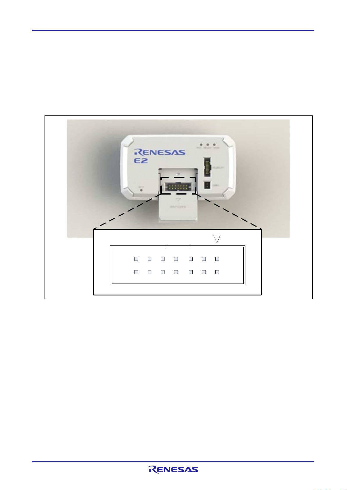
E1/E20/E2/E2 Lite Additional Document 1. Overview
14
13 1
2
1.5 Overview of the Specifications of the External Trigger Input and Output
This section describes the specifications of the external trigger input and output, which is one of E2
extended functions of the E2.
1.5.1 Assignments of the External Trigger Input and Output Pins
The following figure and table show the assignments of the external trigger input and output pins for the
E2 expansion interface.
Figure 1-1 E2 Expansion Interface
R20UT2937EJ0301 Rev.3.01 Page 11 of 45
Jul 1, 2020
Page 12
E1/E20/E2/E2 Lite Additional Document 1. Overview
Pin No.
Input/Output
Description
1
Pin Nos. 1 to 8 are not used.
3
5
7
9
Output
External trigger output (ch. 0)
11
Input
External trigger input (ch. 0)
13 GND
Output signal channels
E2 expansion interface: 2 (ch. 0: pin 9, ch. 1: pin 10)
Conditions for detecting an
Condition for detecting an
Detecting a break or a trigger condition for measuring the current
Table 1-3 Assignments of the External Trigger Input and Output Pins for the E2 Expansion Interface
2
4
6
8
10 Output External trigger output (ch. 1)
12 Input External trigger input (ch. 1)
14 Output A pin for output of the power-supply voltage for the E2 expansion interface
These pins must be left open-circuit.
(1.8 V to 5.0 V)
1.5.2 Specifications of the External Trigger Inputs and Outputs
Table 1-4 Specifications of the External Trigger Inputs and Outputs
Input signal channels E2 expansion interface: 2 (ch. 0: pin 11, ch. 1: pin 12)
Voltage of the E2 expansion
interface
external trigger input
Operation during the input of an
external trigger
external trigger output
Operation during the output of
an external trigger
Note: About 100 µs will be required from the detection of a condition for an external trigger input being satisfied until
the user program is stopped.
• When the power is supplied from the emulator:
supply voltage (1.8V to 5.0 V)
• When the power is not supplied from the emulator: VDD voltage
• Detecting edges (rising, falling, or both)
• Detecting a level (low or high)
• Break*
• Recording the data from measuring the current consumption while the
low or high level is being input
consumption
• When a break is detected, a low- or high-level pulse is output (the
pulse width can be set to times in the range from 1 µsec to 65535
µsec).
• When a trigger condition for measuring the current consumption is
detected, a high-level pulse is output (the pulse width can be set to
times in the range from 1 µsec to 65535 µsec). Otherwise, a high level
is output while a condition is being satisfied.
R20UT2937EJ0301 Rev.3.01 Page 12 of 45
Jul 1, 2020
Page 13
E1/E20/E2/E2 Lite Additional Document 2. Designing the User System
Connector
Type Number
Manufacturer
Specifications
14-pin
7614-6002
3M Japan Limited
14-pin straight type (Japan)
14-pin us
er-system interface cable
14-
pin connector
7614-60
02 or
2514-60
02
User system
Pin 1
Pin 2
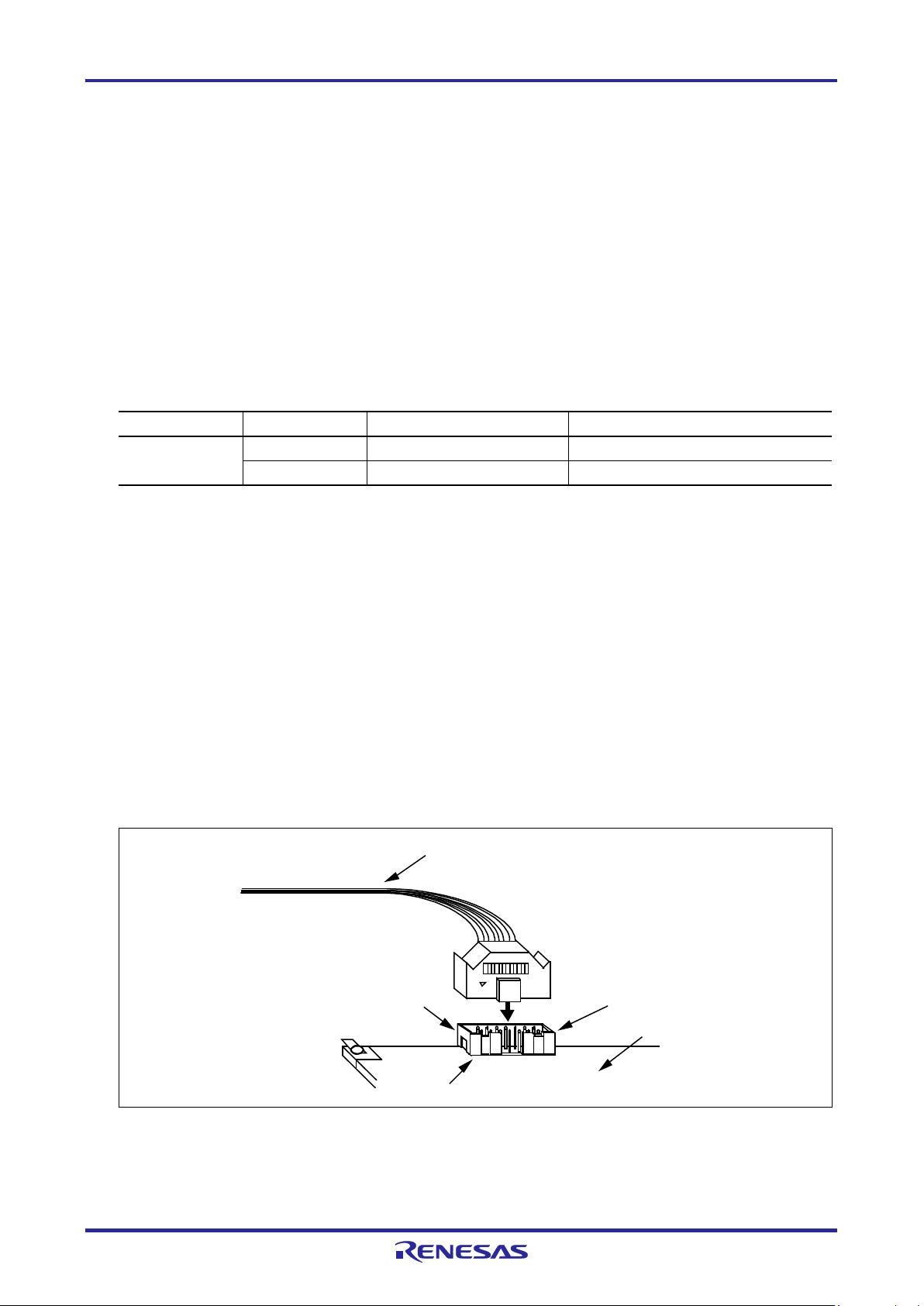
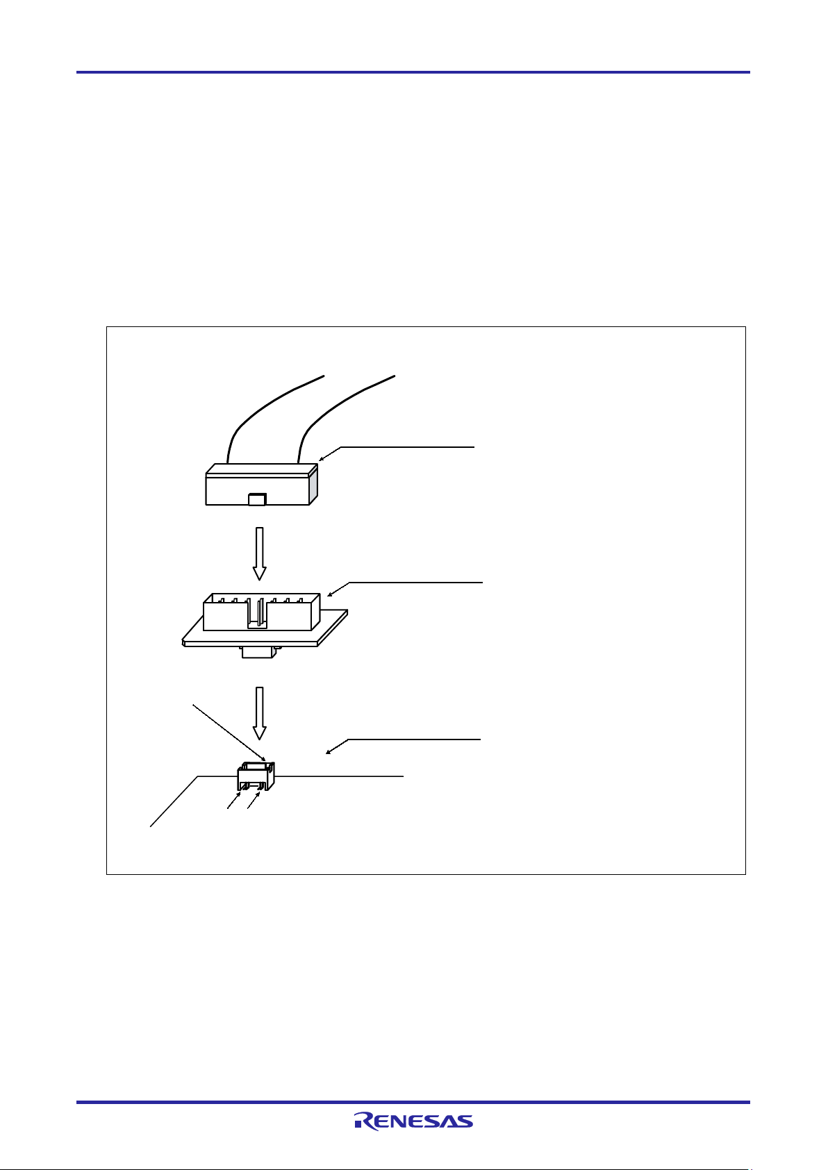
2. Designing the User System
2.1 Connecting the E1/E20/E2/E2 Lite to the User System
To connect the E1/E20/E2/E2 Lite to the user system, a connector for the user system interface cable
must be mounted on the user system.
When designing the user system, read this section of this manual and the hardware manual for the MCU
in use.
2.2 Installing the Connector on the User System
Table 2-1 shows the recommended connectors for the E1/E20/E2/E2 Lite.
Table 2-1 Recommended Connectors
connector
Note: Connection to the 38-pin connector of the E20 is not supported. To use the E20, use the 38-pin to 14-pin
conversion adapter that comes with the E20 for connection to the 14-pin connector on the user system.
2514-6002 3M Limited 14-pin straight type (other countries)
2.2.1 Connecting the User System Interface Cable to the 14-Pin Connector
The following figures show how to connect the user system interface cable to the 14-pin connector of
each emulator.
E1/E2 Lite: Figure 2-1 (Connecting the User System Interface Cable to the 14-Pin Connector of the
E1/E2 Lite Emulator)
E20: Figure 2-2 (Connecting the User System Interface Cable to the 14-Pin Connector of the E20
Emulator)
E2: Figure 2-3 (Connecting the User System Interface Cable to the 14-Pin Connector of the E2
Emulator)
Figure 2-1 Connecting the User System Interface Cable to the 14-Pin Connector of the E1/E2 Lite
Emulator
R20UT2937EJ0301 Rev.3.01 Page 13 of 45
Jul 1, 2020
Page 14
E1/E20/E2/E2 Lite Additional Document 2. Designing the User System
20-pin (1.27-mm pin spacing) user-system
interface cable
13 mm
10.5 mm
User system
14-pin (2.54-mm pin spacing)
connector
7614-6002 or 2514-6002
20-pin (1.27-mm pin
spacing) to 14-pin
(2.54-mm pin spacing)
connector conversion
adapter
10.5 mm
20-pin (1.27-mm pin spacing) to 14-pin
(2.54-mm pin spacing) connector
conversion adapter (top view)
29.0 mm
1
3
Set the switch to position "3"
.
38
-p
i
n t
o 1
4
-p
in
c
on
v
er
si
o
n a
da
p
te
r (
t
op
v
ie
w)
R0E000200CKA00
(
in
c
lu
de
i
n t
h
e E
20
p
ac
ka
g
e)
10
m
m
U
s
er
sy
s
te
m
38-pin user-
sy
s
te
m i
n
te
r
fa
ce
c
ab
le
26.2 mm
9.
4 mm
3
8
-
p
i
n
t
o
1
4
-
p
i
n
conversion adapter
9
.4
m
m
1
4
-p
in
c
on
nector
76
1
4-
60
0
2 o
r
2
51
4
-6
00
2
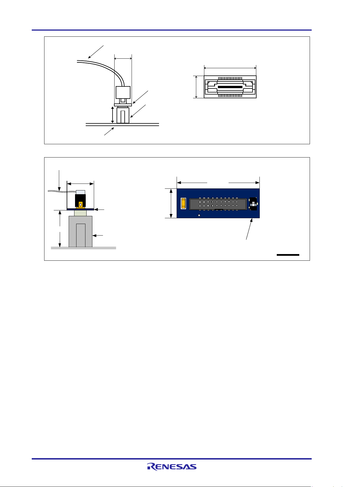
Figure 2-2 Connecting the User System Interface Cable to the 14-Pin Connector of the E20 Emulator
Figure 2-3 Connecting the User System Interface Cable to the 14-Pin Connector of the E2 Emulator
R20UT2937EJ0301 Rev.3.01 Page 14 of 45
Jul 1, 2020
Page 15

E1/E20/E2/E2 Lite Additional Document 2. Designing the User System
CAUTION
Limit to the height on connector periphery:
system.
3
M Japan Ltd.)
For a case where the R0E000200CKA00 is used for connecting the E20 to a 14-pin connector, do not
mount other components with a height of 10 mm or more within 5 mm of the connector on the user
R20UT2937EJ0301 Rev.3.01 Page 15 of 45
Jul 1, 2020
Page 16

E1/E20/E2/E2 Lite Additional Document 2. Designing the User System
CAUTION
Limit to the height on connector periphery:
of 13 mm or more on the user system within a rectangle 2 mm from the edges of the connector.
Type number: 7614-6002 (manufactured by 3M Ltd.) (Japan)
: 2514-6002 (manufactured by 3M Ltd.) (other countries)
The emulator is connected from this direction.
2 mm
2 mm
2 mm
2 mm
Area with limit on mounted components
(heights must be no greater than 13 mm)
CAUTION
Notes on connector insertion and removal:
the cable is connected in the wrong direction, it may be damaged.
Correct example
Incorrect example
If the 20-pin (1.27-mm pin spacing) to 14-pin (2.54-mm pin spacing) connector conversion adapter is
in use and the E2 is to be connected to the 14-pin connector, do not mount components with a height
When connecting or disconnecting the user-system interface cable and the emulator or user system,
grasp the connector cover at the end of the cable. Pulling the cable itself will damage the wiring.
Also, be aware that the user system interface cable has the direction in which it must be inserted. If
R20UT2937EJ0301 Rev.3.01 Page 16 of 45
Jul 1, 2020
Page 17

E1/E20/E2/E2 Lite Additional Document 2. Designing the User System
P
i
n 1
ma
r
k
2
5
.
0
2
3
.
0
6
x
2
.
5
4
=
1
5
.
2
4
(
2
.
5
4
)
0
.4
5
P
in
1
P
in
2
P
i
n
1
3
P
i
n
1
4
P
i
n
1
m
a
r
k
C
o
n
n
e
c
t
o
r
C
o
n
n
e
c
t
o
r
(
t
o
p
v
i
e
w
)
U
n
i
t
:
m
m
2.3 Pin Assignments of the Connector on the User System
2.3.1 14-Pin Connector Specifications
Figure 2-4 shows the specifications of the 14-pin connector.
Table 2-2 on the following pages shows the pin assignments of the 14-pin connector.
Figure 2-4 Emulator Connector Specifications (14 Pins)
R20UT2937EJ0301 Rev.3.01 Page 17 of 45
Jul 1, 2020
Page 18

E1/E20/E2/E2 Lite Additional Document 2. Designing the User System
RL78/G10
Signal *1
Direction *2
2
GND
*3
4
RSTPU
Input
This pin is used to pull up the reset line.
6
RESET_IN
Output
This pin is used to input a reset signal from the user system.
8
VDD
10
RESET_OUT
*4
Input
This pin is used to output a reset signal to the target device.
12
GND
*3
14
GND
*3
*1
For details on the programming software, refer to the following.
*2
“Input” refers to input from the emulator to the user system and
*3
Securely connect pins 2, 12, and 14 of the connector to GND of the user system. These pins are used
*4
Securely connect both pin 10 and pin 13.
*5
This pin is reserved. Perform the open processing.
*6
Connect VDD.
Table 2-2 14-Pin Connector Pin Assignments
Pin
No.
1 R.F.U *5
3 R.F.U *5
5 TOOL0 I/O This pin is used to transmit command/data to the target
device.
7 R.F.U *5
9 EMVDD *6
11 R.F.U *5
13 RESET_OUT *4 Input This pin is used to output a reset signal to the target device.
https://www.renesas.com/RFP
Note
“output” refers to output from the user system to the emulator.
for electrical grounding as well as for monitoring of connection with the user system by the
E1/E20/E2/E2 Lite.
R20UT2937EJ0301 Rev.3.01 Page 18 of 45
Jul 1, 2020
Page 19

E1/E20/E2/E2 Lite Additional Document 2. Designing the User System
MCU
8
VSS
VDD
9
2,12,14
1,3,4,7,11
5 TOOL0
TOOL0
EVDD
VDD
VSS
R.F.U
470 to 510 Ω
1 kΩ
6
10,13
RESET_IN
RESET_OUT
RESET#
1 kΩ
4
RSTPU
VDD
VDD
Note 1
Note 2
14-pin
2.54-mm pitch
connector
Note 4
Note 3
Note 3
Note 3
Reset circuit
Note 5
Note 3 Note 6
2.4 Recommended Circuits between the Connector and the MCU
This section shows recommended circuits for connection between the connector and the MCU when the
E1/E20/E2/E2 Lite is in use. For processing of signals, refer to section 2.5, Notes on Connection.
2.4.1 Connection between the 14-Pin Connector and the RL78 Family MCUs
Figure 2-5 shows a recommended circuit for connection between the 14-pin connector and the RL78
family MCUs.
Figure 2-5 Example of Connection between the 14-Pin Connector and the RL78 Family MCUs
Notes: 1 The circuits and resistance values listed are recommended but not guaranteed. Determine the circuit
2 For processing of pins not used by the E1/E20/E2/E2 Lite, refer to the hardware manual for the
design and resistance values by taking into account the specifications of the target device and noise.
For flash programming for mass production, perform sufficient evaluation about whether the
specifications of the target device are satisfied.
device.
3 The recommended circuit for the RESET# pin differs depending on whether the multiplexed functions
are used. For details on how to handle the RESET# pin, also refer to section 2.5, Notes on
4 The RESET_IN pin is used only in debugging. It is not necessary in flash programming by the
5 Securely connect pins 2, 12, and 14 of the connection to GND of the user system. These pins are
Connection.
programming software.
used for electrical grounding as well as for monitoring of connection with the user system by the
E1/E20/E2/E2 Lite.
6 Securely connect both pin 10 and pin 13.
R20UT2937EJ0301 Rev.3.01 Page 19 of 45
Jul 1, 2020
Page 20

E1/E20/E2/E2 Lite Additional Document 2. Designing the User System
2.5 Notes on Connection
Wiring patterns between the connector and the MCU must be as short as possible (within 50 mm is
recommended). Do not connect the signal lines between the connector and MCU to other signal lines on
the board.
For the handling of pins while the E1/E20/E2/E2 Lite is not in use, refer to the hardware manual for the
MCU.
R20UT2937EJ0301 Rev.3.01 Page 20 of 45
Jul 1, 2020
Page 21

E1/E20/E2/E2 Lite Additional Document 2. Designing the User System
No.
Target Device
Case
Reference
1
RL78/G10
The pin on which the RESET# function is multiplexed is in
Figure 2-6
Reset circuit
6
10,13
RESET_IN
RESET_OUT
4
RSPU
Note 1
14-pin
2.54-mm pitch
connector
MCU
RESET#
<Connection Example 1 of RESET>
(Recommended Circuit)
Note 2
470 to 510 kΩ
1 kΩ
Note 1: It is not necessary in flash programming by the programming software.
Note 2: Connection is unnecessary when there is no reset circuit on the user system.
14-
pin
2.54-mm pitch
connector
MCU
6
10,13
RESET_IN
RESET_OUT
RESET#
4
RSTPU
External circuit
1 kΩ
<Connection Example 2 of RESET>
(when using the P125/KR1/SI01 function which is multiplexed with RESET#)
Figure 2-6 Connection Example 1 of RESET#
Figure 2-7 Connection Example 2 of RESET#
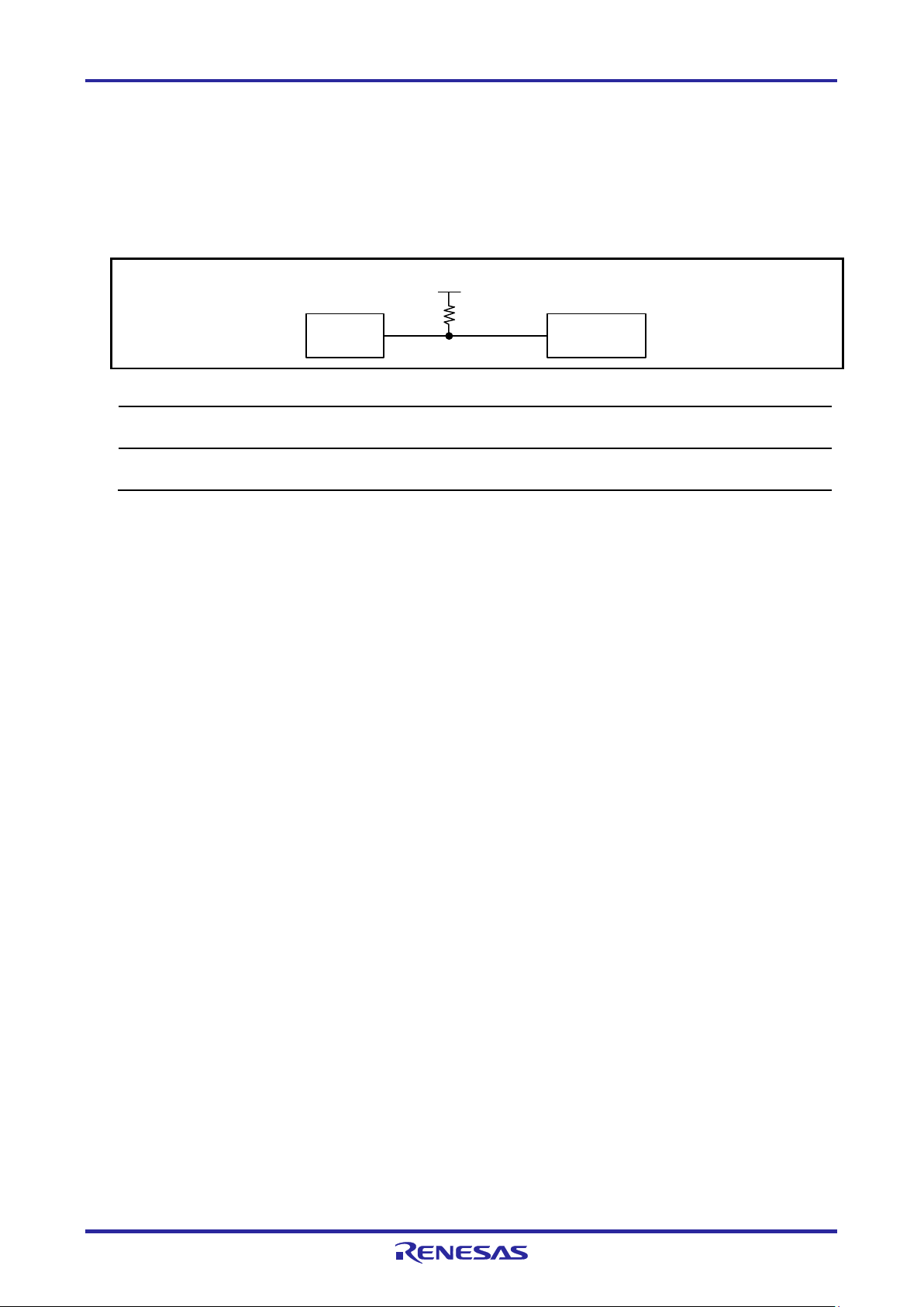
2.5.1 RESET# Pin
The RESET# pin is used by the E1/E20/E2/E2 Lite to monitor the pin state and issue a reset to the
device.
Therefore, a reset signal on the user system is once input to the E1/E20/E2/E2 Lite where it is controlled
by masking and then output to the target device. Connection examples of the RESET# pin section are
shown in Table 2-3 and Figure 2-6 and Figure 2-7.
When flash programming by the programming software is to be performed, the RESET# pin should be
designed so that the reset signal on the user system does not conflict with the reset signal from the
E1/E20/E2/E2 Lite.
Table 2-3 Connection Examples According to the Reset Circuit on the User System
RL78/G1M
RL78/G1N
use for the reset function.
There is no reset circuit if the section enclosed by the dotted
lines described in note 2 for figure 2-6 is removed.
2 The pin on which the RESET# function is multiplexed is in
use for another function.
(when using the P125/KR1 function which is multiplexed with
RESET#)
Figure 2-7
• Do not install capacitors, series resistors, or filters on signal lines; if attempted, correct communication may
not be established. here is an exception, however: capacitors can be inserted between VSS and
RESET_IN.
• The circuits and resistance values listed are recommended but not guaranteed. Determine the circuit design
and resistance values by taking into account the specifications of the target device and noise.
• Securely connect pins 2, 12, and 14 to GND of the user system. These pins are used for electrical
grounding as well as for monitoring of connection with the user system by the E1/E20/E2/E2 Lite. Securely
connect both pin 10 and pin 13.
R20UT2937EJ0301 Rev.3.01 Page 21 of 45
Jul 1, 2020
Page 22
E1/E20/E2/E2 Lite Additional Document 2. Designing the User System
TOOL
0
14-pin
2.54-mm pitch
connector
MCU
TOOL0
1 kΩ
VDD
Do not use adjacent resistors for pull-up of the TCK pin because they may affect or may be affected from other
Do not install capacitors, series resistors, or filters on signal lines; if attempted, correct communication may not
2.5.2 TOOL0 Pin
The E1/E20/E2/E2 Lite uses the TOOL0 pin. Any functions that are multiplexed on this pin are not
available.
Pull up the signals of the TOOL0 pin at 1 kΩ and do not arrange these signal lines in parallel with or
across other high-speed signal lines.
Figure 2-8 Connection Example of the TOOL0 Pin
pins.
be established.
R20UT2937EJ0301 Rev.3.01 Page 22 of 45
Jul 1, 2020
Page 23

E1/E20/E2/E2 Lite Additional Document 2. Designing the User System
2.5.3 GND
The pins of the connector marked "GND" must be at the same ground level as the VSS pin of the MCU.
2.5.4 VDD
Connect the VDD of the connector to the VDD (power supply) of the user system.
Use the emulator within the power supply voltage of 1.8 V to 5.5 V and within the operating voltage
range of the MCU.
When power is supplied to the user system from other than the emulator, the E1/E20/E2/E2 Lite
consumes the power supply for the last output and first input buffers of the emulator.
E1: 3.3 V: approximately 20 mA, 5.0 V: approximately 40 mA
E20: 3.3 V: approximately 40 mA, 5.0 V: approximately 100 mA
E2: 3.3 V: approximately 20 mA, 5.0 V: approximately 40 mA
E2 Lite: 3.3 V: approximately 20 mA, 5.0 V: approximately 40 mA
The E1/E2/E2 Lite can supply power to a simple evaluation system.
E1: Can supply power of 3.3 V or 5.0 V, up to 200 mA.
E2: Can supply power of 1.8 V to 5.0 V, up to 200 mA.
E2 Lite: Can supply power of 3.3 V, up to 200 mA.
When using the power supply function of the E1/E2/E2 Lite, check the voltage supplied to the user
system. Particularly when the 5.0-V supply option is selected, the voltage depends on the USB VBUS
power-supply voltage.
E1: The voltage may drop by 0.5 V or more below 5.0 V.
E2: The voltage may drop by 0.3 V or more below 5.0 V.
The on-chip debugging circuit in the device operates during on-chip debugging. Therefore current
consumption of the device increases. When correctly evaluating current consumption of the device, do
not connect the E1/E20/E2/E2 Lite.
Power supply from the E1/E2/E2 Lite depends on the quality of the USB power supply of the host machine, and
as such, precision is not guaranteed. When writing a program that requires reliability, do not use the power
supply function of the E1/E2/E2 Lite. Use a stable, separate power supply for the user system. When writing a
program for mass production processes, use the Renesas Flash Programmer.
For details on the programming software, refer to:
https://www.renesas.com/RFP
R20UT2937EJ0301 Rev.3.01 Page 23 of 45
Jul 1, 2020
Page 24
E1/E20/E2/E2 Lite Additional Document 2. Designing the User System
WARNING
Warning for Turning the Power On/Off:
When supplying power, ensure that there are no shorts between VDD and GND. Only connect the
E1/E20/E2/E2 Lite after confirming that there are no mismatches of alignment on the user system
port connector. Incorrect connection will result in the host machine, the E1/E20/E2/E2 Lite, and the
user system emitting smoke or catching fire.
R20UT2937EJ0301 Rev.3.01 Page 24 of 45
Jul 1, 2020
Page 25
E1/E20/E2/E2 Lite Additional Document 2. Designing the User System
Emulator
control
circuit
User-side
connector
100 kΩ × 2
100 kΩ
RSTPU
VDD
4
8
22 Ω
74
LVC125
74LVC8T245
3.3 V
EMVDD
TOOL0
5
74
LVC125
EMVDD
74LVC125
74LVC8T245
6
RESET_IN
74LVC125
74LVC8T245
22 Ω
10
RESET_OUT
3.3 V
74
LVC125
22 Ω
100
kΩ
GND
14
3.3 V
74LVC8T245
13
RESET_OUT
22 Ω
470 Ω
Self-recovering
fuse
2,12
GND
Power-supply circuit
(only for use in the mode to
supply power to the user
system)
EMVDD
EMVDD
9
22
Ω
22 Ω
74LVC2T245
100 kΩ
74LVC125
100 kΩ
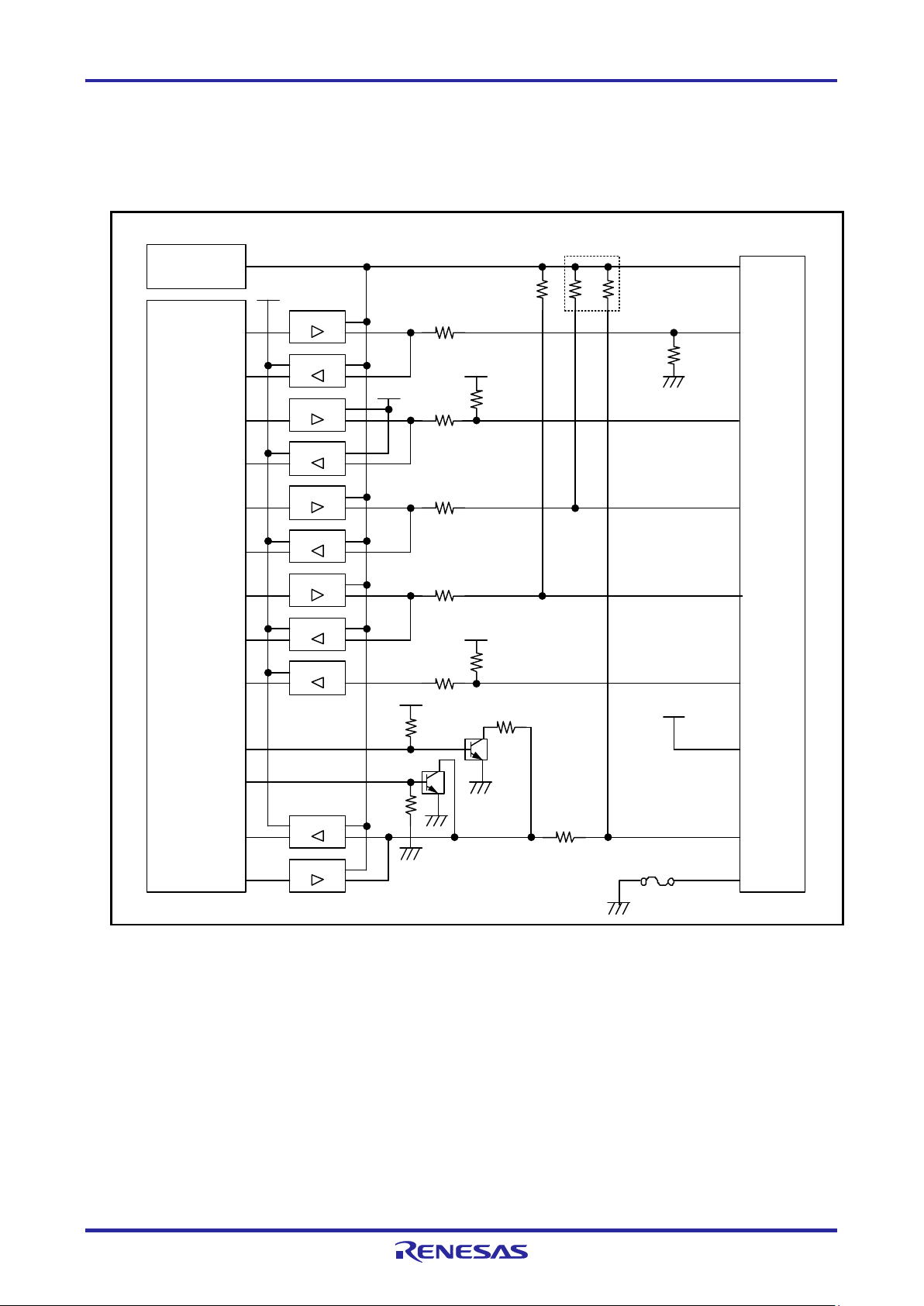
2.6 Internal Circuits of the Emulator
2.6.1 Internal Circuits of the E1 (when the RL78 Family is Connected)
Figure 2-9 shows the internal circuits of the E1 with the RL78 family connected.
Figure 2-9 Internal Circuit of the E1 (when the RL78 Family is Connected)
R20UT2937EJ0301 Rev.3.01 Page 25 of 45
Jul 1, 2020
Page 26
E1/E20/E2/E2 Lite Additional Document 2. Designing the User System
Emulator
control
circuit
100 kΩ
RSTPU
VDD
4
8
22
Ω
74LVC
125
74LVC
8T
245
3.3
V
EMVDD
TOOL0
5
74
LVC
125
EMVDD
74LVC125
74LVC8T245
6
RESET_
IN
74LVC125
74LVC8
T245
22 Ω
10
RESET_OUT
3.3
V
74
LVC125
22 Ω 100 kΩ
GND
14
3.3 V
74LVC8T
245
13
RESET_OUT
22 Ω
470 Ω
2,12
GND
EMVDD
EMVDD
9
22 Ω
22 Ω
74LVC2T245
100 k
Ω
74
LVC
125
100 k
Ω
× 2100
kΩ
Self
-recovering
fuse
User-
side
connector
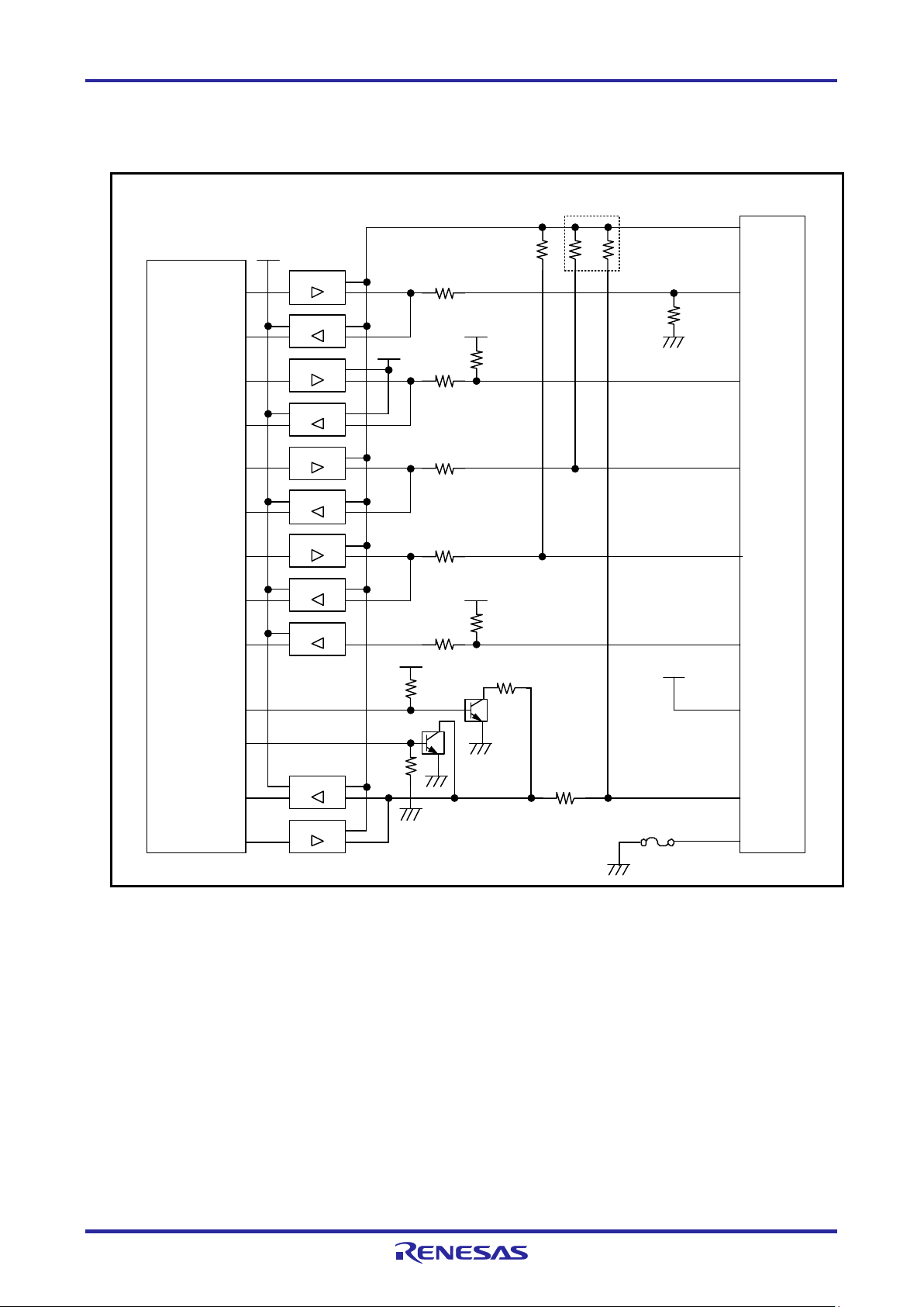
2.6.2 Internal Circuits of the E20 (when the RL78 Family is Connected)
Figure 2-10 shows the internal circuits of the E20 with the RL78 family connected.
Figure 2-10 Internal Circuits of the E20 (RL78 Family)
R20UT2937EJ0301 Rev.3.01 Page 26 of 45
Jul 1, 2020
Page 27

E1/E20/E2/E2 Lite Additional Document 2. Designing the User System
3 MΩ
RSTPU
VDD
4
8
3.3 V
EMVDD
TOOL0
5
EMVDD
6
RESET_IN
10
RESET_OUT
3
.3 V
100 kΩ
GND
14
13
RESET_OUT
2,12
GND
EMVDD
EMVDD
9
1 MΩ
74LVC1T45
74LVC1T45
74LVC1T45
74LVC1T45
74
LVC1T45
0.1 µF
100 kΩ
74
LVC1T45
Emulator
control
circuit
Power-supply circuit
(only for use in the mode to
supply power to the user
system)
User-side
connector
Self-recovering
fuse
47 Ω
47 Ω
47 Ω
47 Ω
47 Ω
1 MΩ × 2
74LVC1T45
74LVC8T245
74
LVC8T245
74LVC8T245
2.6.3 Internal Circuits of the E2 (when the RL78 Family is Connected)
Figure 2-11 shows the internal circuits of the E2 with the RL78 family connected.
Figure 2-11 Internal Circuits of the E2 (RL78 Family)
Set the switch on the 20-pin (1.27-mm pin spacing) to 14-pin (2.54-mm pin spacing) connector
conversion adapter to position “3”.
R20UT2937EJ0301 Rev.3.01 Page 27 of 45
Jul 1, 2020
Page 28

E1/E20/E2/E2 Lite Additional Document 2. Designing the User System
Emulator
control
circuit
RSTPU
VDD
4
8
47 Ω
74LVC125
74LVC8T245
3.3 V
TOOL0
5
74LVC125
74LVC125
74LVC8T245
6
RESET_IN
74LVC125
74LVC8T245
47 Ω
10
RESET_OUT
3.3 V
47 Ω
100 kΩ
GND
14
74LVC8T245
13
RESET_OUT
47 Ω
2,12
GND
Power-supply circuit
(only for use in the mode to
supply power to the user
system)
EMVDD
9
47 Ω
47 Ω
74LVC8T245
74LVC125
100 kΩ × 5
1 MΩ
1,3,7,11
74LVC125
74LVC8T245
47 Ω
User-side
connector
Self-recovering
fuse
2.6.4 Internal Circuits of the E2 Lite (when the RL78 Family is Connected)
Figure 2-12 shows the internal circuits of the E2 Lite with the RL78 family connected.
Figure 2-12 Internal Circuits of the E2 Lite (when the RL78 Family is Connected)
R20UT2937EJ0301 Rev.3.01 Page 28 of 45
Jul 1, 2020
Page 29

E1/E20/E2/E2 Lite Additional Document 2. Designing the User System
2.7 Notes on Designing the User System
2.7.1 Isolator for the E1
For a debugging environment where there is a difference in potential between the GND of the user
system and that of the host PC, use the isolator for the E1 emulator (R0E000010ACB20) which is
separately available from Renesas.
That is, use the isolator for the E1 (R0E000010ACB20) with the E2/E2 Lite in such situations.
2.7.2 Low-Voltage OCD Board
Since the RL78-S1 core device needs 4.5 V to 5.5 V as the voltage for rewriting flash memory, if the
voltage is less than 4.5 V, the debugging functions that require flash memory to be rewritten (e.g.,
program download) cannot be operated. When debugging with a voltage less than 4.5 V, the lowvoltage OCD board (R0E510Y47LVB00 or R0E510Y16LVB00) which is sold separately must be
prepared. For details on the low-voltage OCD board, refer to the user's manual.
When the low-voltage OCD board is in use, none of the extended functions supported by the E2
emulator are available.
The low-voltage OCD board cannot be used for RL78/G1M and RL78/G1N.
R20UT2937EJ0301 Rev.3.01 Page 29 of 45
Jul 1, 2020
Page 30
E1/E20/E2/E2 Lite Additional Document 2. Designing the User System
User-system interface cable for
E1 (R0E000010KCE00),
E2 Lite (RTE0T0002LKCE00000R), or
E2 (RTE0T00020KCE00000R) and
20-pin (1.27-mm pin spacing) to 14-pin (2.54-mm pin spacing)
connector conversion adapter
Small connector conversion adapter for the E1
(R0E000010CKZ11)
14-pin connector on the user system (TFM-107-02-L-D
(SMT) or TFM-107-01-L-D (DIP)): manufactured by
Samtec, Inc.
User systemPin 1 Pin 13
Orientation key
CN2
CN1
2.7.3 Small Connector Conversion Adapter for the E1
A small connector conversion adapter for the E1 (R0E000010CKZ11) is separately available from
Renesas for user system boards which are too small to mount the 14-pin connector that is the standard
connector for the E1, E2 and E2 Lite. By using the adapter, you can reduce the area taken up by the
connector mounted on your system.
However, when you use the small connector conversion adapter for the E1, be aware that the pin
assignments of the connector differ from those of the standard interface connector for the E1, E2 and E2
Lite. The pin assignments on the 14-pin connector when the small connector conversion adapter for the
E1 is used are shown in Table 2-4.
The small connector conversion adapter for the E1 can also be used with the E2 and E2 Lite.
Figure 2-13 Usage of the Small Connector Conversion Adapter for the E1
R20UT2937EJ0301 Rev.3.01 Page 30 of 45
Jul 1, 2020
Page 31
E1/E20/E2/E2 Lite Additional Document 2. Designing the User System
Pin
RL78/G10
Signal *1
Direction *2
1
GND
*3
3
VDD
5
RESET_OUT
*4
Input
This pin is used to output a reset signal to the target device.
7
RESET_OUT
*4
Input
This pin is used to output a reset signal to the target device.
9
R.F.U
*5
11
RSTPU
Input
This pin is used to pull up the reset line.
13
EMVDD
*6
Table 2-4 Connector Pin Assignments when the Small Connector Conversion Adapter for the E1 is
Used
No.
2 R.F.U *5
4 R.F.U *5
6 GND *3
8 R.F.U *5
10 TOOL0 I/O This pin is used to transmit command/data to the target
device.
12 RESET_IN Output This pin is used to input a reset signal from the user system.
14 GND *3
*1 For details on the programming software, refer to the following.
https://www.renesas.com/RFP
*2 “Input” refers to input from the emulator to the user system and
“output” refers to output from the user system to the emulator.
*3 Securely connect pins 1, 6, and 14 of the connector to GND of the user system. These pins are used for
electrical grounding as well as for monitoring of connection with the user system by the E1/E20/E2 Lite.
*4 Securely connect both pin 5 and pin 7.
*5 This pin is reserved. Perform the open processing.
*6 Connect VDD.
Note
R20UT2937EJ0301 Rev.3.01 Page 31 of 45
Jul 1, 2020
Page 32

E1/E20/E2/E2 Lite Additional Document 3. Notes on Usage
3. Notes on Usage
3.1 Turning the Power On/Off
Turn the power of the E1/E20/E2/E2 Lite and the user system following the procedure below.
3.1.1 When a Separate Power Supply is Used for the User System
<When using the emulator>
(1) Check that the power is off.
Check that the user system is turned off. When using the E20, check its power switch is off.
(2) Connect the user system.
Connect the emulator and the user system with a user-system interface cable.
When the external trigger input/output function is to be used with the E2, connect the pins to be
used.
(3) Connect the host machine and turn on the emulator.
Connect the emulator and the host machine with a USB interface cable. The E1/E2/E2 Lite is turned
on by connecting the USB interface cable. When using the E20, turn on its power switch.
(4) Launch the emulator debugger or programming software.
Launch the emulator debugger or programming software.
(5) Turn on the user system.
Turn on the user system.
(6) Launch the emulator debugger or connect the programming software to the emulator.
Connections may vary depending on software.
<When finished using the emulator>
(1) Close the emulator debugger or disconnect the emulator from the programming software.
Disconnections may vary depending on software.
(2) Turn off the user system.
Turn off the user system.
(3) Close the emulator debugger or the programming software.
Close the emulator debugger or the programming software.
(4) Turn off the emulator and disconnect the emulator.
When using the E20, turn off its power switch. Disconnect the USB interface cable from the
E1/E2/E2 Lite. The E1/E2/E2 Lite is turned off by disconnecting from the USB interface cable.
(5) Disconnect the user system.
Disconnect the user system interface cable from the user system.
R20UT2937EJ0301 Rev.3.01 Page 32 of 45
Jul 1, 2020
Page 33

E1/E20/E2/E2 Lite Additional Document 3. Notes on Usage
CAUTION
Notes on the User System Power Supply:
When the external trigger input/output function is to be used with the E2, disconnect the pins that
were in use.
While the power of the user system is on, do not turn off the host machine, unplug the USB interface
cable, or turn off the power switch of the E20.
The user system may be damaged due to leakages current.
R20UT2937EJ0301 Rev.3.01 Page 33 of 45
Jul 1, 2020
Page 34

E1/E20/E2/E2 Lite Additional Document 3. Notes on Usage
3.1.2 When Power is Supplied to the User System from the Emulator (E1/E2/E2 Lite Only)
<When using the emulator>
(1) Connect the user system.
Connect the emulator and the user system with a user-system interface cable.
When the external trigger input/output function is to be used with the E2, connect the pins to be
used.
(2) Connect the host machine and turn on the emulator.
Connect the emulator and the host machine with a USB interface cable, then turn on the emulator.
(3) Launch the emulator debugger or programming software.
Launch the emulator debugger or programming software and select the setting of power supply to
the user system.
(4) Connect the emulator debugger or programming software to the emulator.
Connections may vary depending on software.
<When finished using the emulator>
(1) Disconnect the emulator debugger or programming software from the emulator.
Disconnections may vary depending on software.
(2) Close the emulator debugger or programming software.
Close the emulator debugger or programming software.
(3) Turn off the emulator and disconnect the emulator.
Disconnect the USB interface cable from the emulator, then turn off the emulator.
(4) Disconnect the user system.
Disconnect the user system interface cable from the user system.
When the external trigger input/output function is to be used with the E2, disconnect the pins that
were in use.
R20UT2937EJ0301 Rev.3.01 Page 34 of 45
Jul 1, 2020
Page 35

E1/E20/E2/E2 Lite Additional Document 3. Notes on Usage
3.2 Power Supply Function of the E1/E2/E2 Lite
When using the power supply function of the E1/E2/E2 Lite, check the voltage supplied to the user
system. Particularly when the 5.0-V supply option is selected, the voltage depends on the USB VBUS
power-supply voltage.
E1: The voltage may drop by 0.5 V or more below 5.0 V.
E2: The voltage may drop by 0.3 V or more below 5.0 V.
Note that the E2 Lite supports power supply of 3.3 V only.
For the E2, 1.8 V to 5.0 V can be specified as the supply voltage and 0 V can also be specified during
execution of the user program. However, when an extended function is specified, do not set the voltage
to 0 V during execution of the user program.
When the supply voltage is set to 0 V by the E2 during execution of the user program, continued
debugging may not be possible if the voltage on the TOOL0 pin is unstable during the voltage drop. Also
refer to the notes in section 2.5.2, TOOL0 Pin.
R20UT2937EJ0301 Rev.3.01 Page 35 of 45
Jul 1, 2020
Page 36

E1/E20/E2/E2 Lite Additional Document 3. Notes on Usage
00000h
Security ID area
10 bytes
000C3h
Reset vector area
2 bytes
00002h
Debug monitor area
2 bytes
00004h
On-chip debug
option byte area
1 byte
000C4h
000CEh
Debug monitor area
10 bytes
000D8h
Stack area for debugging
10 bytes
Area for pseudo-RRM/
pseudo-DMM
4 bytes
Internal
ROM end
address
Internal ROM
space
Internal
RAM end
address
Internal RAM
space
3.3 MCU Resources to be Occupied
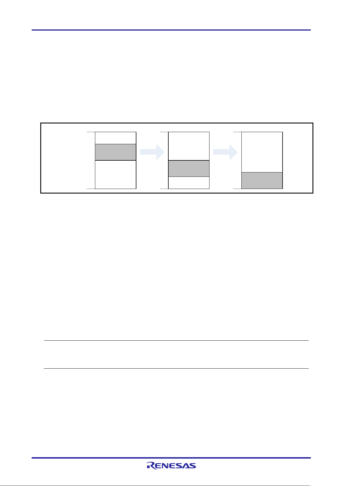
Figure 3-1 shows the areas which are occupied by the E1/E20/E2/E2 Lite for debugging.
These areas (shaded sections) are used for debugging. These areas should not be changed to save the
user program or data. If a change is made, control by the E1/E20/E2/E2 Lite is no longer possible.
However, when "No" is selected in the [Permit flash programming] property of the debugger, the internal
ROM spaces shown in Figure 3-1 are not used (only the internal RAM spaces are used).
When selecting not to permit flash memory rewriting with the debugger's property, also refer to section
3.3.3, Setting an On-Chip Debugging Option Byte.
Figure 3-1 MCU Resources to be Occupied
*1 The reset vector area is used by the program for the E1/E20/E2/E2 Lite when performing debugging
with the E1/E20/E2/E2 Lite. If the contents of the reset vector area are changed, control by the
E1/E20/E2/E2 Lite is no longer possible.
3.3.1 Securing an Area for the Debugging Monitor Program
You may need to secure the area to which the debugging monitor program is to be allocated. The
monitor program initializes the debugger communications interface and handles processing to make the
CPU run or break execution.
The user program or data must not be placed within 23 bytes of the on-chip debugging option byte.
In addition, the reset vector must be changed if it points to an address to which the monitor program is
allocated.
The working RAM for the pseudo-RRM/pseudo-DMM starts at addresses 0x02 and 0x03.
The internal ROM spaces, including the debug monitoring area, are erased when the debugger is
closed.
[Securing the area]
Specifically securing the area for the monitor program is not necessarily required if the user program
does not use the area.
However, to avoid problems that may occur while the debugger is starting up, we recommend securing
this area in advance by using a build tool or some other means.
R20UT2937EJ0301 Rev.3.01 Page 36 of 45
Jul 1, 2020
Page 37
E1/E20/E2/E2 Lite Additional Document 3. Notes on Usage
Stack area for
debugging
10 bytes
Stack area
Available space
in internal RAM
0xFFE60
0xFFEDF
Stack area for
debugging
10 bytes
Stack area
Available space
in internal RAM
0xFFE60
0xFFEDF
Stack area for
debugging
10 bytes
Stack area
0xFFEDF
0xFFE60
*1
If the value of the on-chip debugging option byte set in the device disables on-chip debugging
3.3.2 Securing a Stack Area for Debugging
The debugger requires 10 bytes as a stack area for debugging. Since this area is allocated immediately
after the stack area, the address of this area varies depending on the stack increase and decrease. That
is, 10 extra bytes are consumed for the stack area used.
Make sure the stack area for debugging does not exceed the range of the internal RAM space.
Figure 3-2 shows an example in which the stack area has increased with the start address of the
internal RAM space being 0xFFE60.
Figure 3-2 Variation of Address of Stack Area for Debugging
3.3.3 Setting an On-Chip Debugging Option Byte
This is the area for the security setting to prevent the flash memory from being read by an unauthorized
person.
For settable values, refer to the user's manual for each MCU.
[Setting an on-chip debugging option byte]*1
Set the on-chip debugging option byte in either of the following ways.
(a) Embed the on-chip debugging option byte at address 0xC3 in the user program.
(b) Set the on-chip debugging option byte by the build tool.
For details on the setting method, refer to the user's manual for the build tool.
(OCDENSET = 0), the debugger cannot be started when "No" is selected in the [Permit flash
programming] property of the debugger. If a setting to enable flash programming is made, though the
debugger can be started, the flash memory will be in an erased state when the debugger is started.
R20UT2937EJ0301 Rev.3.01 Page 37 of 45
Jul 1, 2020
Page 38

E1/E20/E2/E2 Lite Additional Document 3. Notes on Usage
Address
Value
0x000C4
0x01
0x000C6
0x45
0x000C8
0x89
0x000CA
0xCD
0x000CC
0x12
Notes:
1
When connecting a debugger to a device for which the security ID has been set, the security ID
2 The setting "0xFFFFFFFFFFFFFFFFFFFF", in which the value at all addresses is "0xFF", is
3.3.4 Setting a Security ID
This setting is required to prevent the memory from being read by an unauthorized person. Embed a
security ID at addresses 0xC4 to 0xCD in the internal flash memory. The debugger starts only when the
security ID that is set during debugger startup and the security ID set at addresses 0xC4 to 0xCD match.
If the ID codes do not match, the debugger manipulates the target device in accordance with the value
set to the on-chip debug option byte area (refer to the hardware manual for each MCU).
If the user has forgotten the security ID to enable debugging, erase the flash memory and set the
security ID again.
Set the security ID in either of the following ways. When both methods (a) and (b) are carried out at the
same time, method (b) has priority.
(a) Embed the security ID at addresses 0xC4 to 0xCD in the user program.
For example if the security ID is embedded as follows, the security ID set by the debugger
is ″0123456789ABCDEF1234″ (not case-sensitive).*
(b) Set the security ID by common options of the build tool.
For details on the setting method, refer to the user's manual for the build tool.
Table 3-1 Example of Security ID Setting
0x000C5 0x23
0x000C7 0x67
0x000C9 0xAB
0x000CB 0xEF
0x000CD 0x34
1, *2
needs to be entered in the debugger. For details on the authentication method, refer to the
user's manual for the debugger in use.
prohibited.
3.3.5 Area for Pseudo-RRM/Pseudo-DMM
To use the pseudo-RRM/pseudo-DMM function in the RL78-S1 core device, a part (4 bytes) of the RAM
area is used for the pseudo-RRM/pseudo-DMM function. Information, such as whether this area can be
allocated by the build tool, can be confirmed in the user's manual for the build tool.
R20UT2937EJ0301 Rev.3.01 Page 38 of 45
Jul 1, 2020
Page 39

E1/E20/E2/E2 Lite Additional Document 3. Notes on Usage
3.4 Reset
3.4.1 Operation after a Reset
After an external pin reset or internal reset, the monitor program performs debug initialization processing.
Consequently, the time from reset occurrence until user program execution differs from that in the actual
device operation. If “No” is selected in Permit flash programming in property of the debug tool, the time
until the user program is executed compared with the time when “Yes” is selected is delayed (max. 100
ms).
3.4.2 SP Value after a Reset
While debugging with the E1/E20/E2/E2 Lite, the SP value after a reset becomes FED0h.
3.5 Flash Memory
3.5.1 Operation for Voltages Not Permitting Flash Memory Rewriting
When a voltage with which rewriting or erasure of flash memory cannot be performed has been selected
or flash programming has been disabled with the debugger's property, the debugger operations that
rewrite flash memory will cause an error in the debugger and the operations will be invalidated.
3.5.2 Notes on Flash Memory Rewriting
In the RL78-S1 core device, a pin reset is always necessary for rewriting of flash memory. For this
reason, a pin reset always occurs at debugger operations (download, rewriting of flash memory from a
memory window, etc.) that accompany rewriting of flash memory.
Since a part of the RAM area (0FFEC6h to 0FFECFh) is used by the E1/E20/E2/E2 Lite at rewriting of
flash memory, the RAM data will be rewritten.
3.6 RESET# Multiplexed Pin
The RESET# pin has multiplexed pin functions. Therefore, if the following conditions are all satisfied,
control by the E1/E20/E2/E2 Lite is no longer possible.
The reset/port multiplexed pin is used as a port (PORTSELB = 0) due to the option byte setting
(C1h).
The option byte setting (C1h) has been rewritten during a break.
"Yes" is selected in the [Mask INTERNAL RESET signal] property of the debugger.
R20UT2937EJ0301 Rev.3.01 Page 39 of 45
Jul 1, 2020
Page 40

E1/E20/E2/E2 Lite Additional Document 3. Notes on Usage
3.7 MCUs that are Used in Debugging
3.7.1 Usage in Mass-Production
MCUs that are connected to the E1/E20/E2/E2 Lite and used in debugging are placed under stress by
repeated programming of flash memory during emulation. Do not use MCUs that were used in
debugging in mass-production for end users.
Also, as the E1/E20/E2/E2 Lite program is written to the MCU while debugging, do not save the
contents of the MCU flash memory which were used for debugging nor use them as the ROM data for
products.
3.7.2 Standalone Operation
After downloading a load module file to the device to for on-chip debugging, do not check the operation
of this device without E1/E20/E2/E2 Lite.
A device after debugging contains the specific program for on-chip debugging, so it is different from
actual operation.
3.8 Final Evaluation of the User Program
Before entering the mass-production phase, be sure to perform a final evaluation of the program which
has been written to the flash ROM by the Renesas Flash Programmer programming software or a flash
programmer, without the emulator connected.
R20UT2937EJ0301 Rev.3.01 Page 40 of 45
Jul 1, 2020
Page 41

E1/E20/E2/E2 Lite Additional Document 3. Notes on Usage
3.9 Debug Functions
3.9.1 Step Execution
(1) Cautions on using step-in (step execution)
The value of some SFRs (special function registers) might remain unchanged while stepping into
code. If the values of the SFRs do not change while stepping into code, operate the microcontroller
by continuously executing the instructions instead of executing them in steps.
Stepping into code: Instructions in the user-created program are executed one by one.
Continuous execution: The user-created program is executed from the current PC value.
3.9.2 [Go to Here]
If [Go to Here] is selected, event breakpoints that have been set so far will be temporarily invalidated.
3.9.3 Debugging in Standby Mode
The break is an interrupt function of the CPU. Standby mode is released by the break generated by
using the following debugging functions.
<1> Forced break
<2> Step execution of the standby instruction (Stops the user program after execution instruction)
<3> Short break generated by the pseudo-RRM function (Break When Readout)
<4> Short break generated by the pseudo-DMM function (Break When Write)
<5> Short break generated by setting a breakpoint while executing the user program
3.9.4 Pseudo-Real-Time RAM Monitor Function or Pseudo-Dynamic Memory Modification Function
Note the following points when using the pseudo-real-time RAM monitor (RRM) function or the pseudoDynamic Memory Modification (DMM) function.
• Standby mode (HALT or STOP) may be cancelled during monitoring.
• The pseudo-RRM function or the pseudo-DMM function does not operate while the CPU operating
clock is stopped.
• When the number of monitoring points is numerous, the response of the debugger becomes slow.
• Influence of the debugger response becomes small by using a watch panel instead of a memory
panel.
• Four bytes of the RAM area are used when the pseudo-RRM and pseudo-DMM functions are used.
The RAM area to be used when using the pseudo-RRM and pseudo-DMM functions should be set by
the build tool.
(For details on setting the area, refer to the user's manual for the build tool.)
If no area is set, the four bytes at the beginning of the RAM area will be used.
R20UT2937EJ0301 Rev.3.01 Page 41 of 45
Jul 1, 2020
Page 42

E1/E20/E2/E2 Lite Additional Document 3. Notes on Usage
3.9.5 Software Break Functions
The RL78-S1 core device does not have the software break function. The hardware break function can
be used alternatively but a break will occur several instructions after the breakpoint because the
hardware break function generates a break after execution of the instruction at the breakpoint. Note that
if a branch occurs between the breakpoint and the point where program execution stops, the break
appears to have not occurred at the breakpoint in some cases.
3.9.6 Extended Functions of the E2
3.9.6.1 Solution for the Tuning of Current Consumption
For notes on the solution for the tuning of current consumption, refer to the application note.
3.9.6.2 External Trigger Input and Output
• Use the value of the high-level voltage which can be input to the external trigger input in accordance
with the value that has been set for the power-supply voltage of the E2 expansion interface.
• The value of the high-level voltage which is output on the external trigger outputs depends on the
value that has been set for the power-supply voltage of the E2 expansion interface.
• When a break is detected and a low or high pulse is output with the external trigger output function,
output of the pulse lags behind stopping of the program by a time between over a hundred
microseconds and hundreds of milliseconds.
The time lag is up to 80 ms when the operating frequency is 1.25 MHz.
R20UT2937EJ0301 Rev.3.01 Page 42 of 45
Jul 1, 2020
Page 43

Description
Page
Summary
All
Information on the E2 emulator was added.
37
Notes on using the RESET# multiplexed pin were added to section 3.6.
38
A note on standalone operation of the device was added to section 3.7.2.
3.01
Jul 1, 2020
All
Information on the RL78/G1M and RL78/G1N were added.
Revision History
Rev. Date
3.00 Jul 1, 2017
Page 44

E1/E20/E2 Emulator, E2 Emulator Lite
Additional Document for User's Manual
(Notes on Connection of RL78)
Publication Date: Jul 1, 2020 Rev.3.01
Published by: Renesas Electronics Corporation
Page 45

E1/E20/E2 Emulator, E2 Emulator Lite
1
Additional Document for User’s Manual
(Notes on Connection of RL78)
R20UT2937EJ030
 Loading...