

Page 1
Emulation Adapter for
E2H
RTE7702012EAB00000J
ser’ s Manual
Rev. 1.10 Nov 2019
User's Manual
All information contained in these materials, including products and product specifications,
website (http://www.renesas.com).
www.renesas.com
Cover
the RH850/E2UH and
Groups
U
represents information on the product at the time of publication and is subject to change by
Renesas Electronics Corp. without notice. Please review the latest information published by
Renesas Electronics Corp. through various means, including the Renesas Electronics Corp.
Page 2

Notice
on of
1. Descriptions of circuits, software and other related information in this document are provided only to illustrate the operati
semiconductor products and application examples. You are fully responsible for the incorporation or any other use of the circuits,
software, and i nformation i n the desi gn of your produc t or syste m. Renesa s Electr onics discla ims any and al l liabilit y for any loss es and
damages incurred by you or third par ties arising from the use of these circuits, software, or information.
2. Renesas Elec tronics hereby expr essly discla ims any warranties against and liability for infringement or any other clai ms involving patents,
copyrights, or other intellectual prop erty rights of third part ies, by or arising from the use of Renesas Electronics pr oducts or technical
information described in this document, including but not limited to, the product data, drawings, charts, programs, algorithms, and
application examples.
3. No license, expr ess, impli ed or otherwi se, is gra nted hereb y under an y patents , copyright s or other intell ectual prop erty rights of Renesas
Electronics or others.
4. You shall not alter , modify, copy, or revers e engineer any Renes as Electr onics product , whether in whole or in part. Renesas Electronics
disclaims any and all liability for any losses or damages incurred by you or third parties arising from such alteration, modification,
copying or reverse engineering.
5. Renesas Electroni cs products are cla ssified accordi ng to the following two qua lity grades: “Sta ndard” and “High Quali ty”. The intended
applications for each Renesas Electronics product depends on the product’s quality grade, as indicated below.
“Standard”: Computers; office equipment; communications equipment; test and measurement equipment; audio and visual equipment;
home electronic appliances; machine tools; personal electronic equipment; industrial robots; etc.
“High Quality”: Transportation equipment (automobiles, trains, ships, etc.); traffic control (traffic lights); large-scale communication
equipment; key financial terminal systems; saf ety control equipment; etc.
Unless expressl y designated a s a high reli abilit y product or a product for ha rsh environ ments in a Renes as Elec tronics data sheet or ot her
Renesas Electr onic s docum ent, Ren esa s El ectr onic s pr oduc ts a re not i ntended or a uthor i z ed for us e in produc t s or systems tha t may pose a
direct threat to huma n life or bodily injury (ar tificial life supp ort devices or systems; s urgical implantations ; etc.), or may cause ser ious
property damage (s pace system; unders ea repeaters ; nuclear power cont rol systems; a ircraft control systems; key pla nt systems; milit ary
equipment; etc. ). Renesa s El ectroni cs dis claims a ny and al l liab ilit y for any damages or los ses i ncurred b y you or any thi rd parties arising
from the use of any Renes as Electronics product that is inconsistent with any Renesa s Electronics data sheet, us er’s manual or other
Renesas Electronics document.
6. When using Renesas Elect roni cs product s, r efer to t he lates t product informa tion ( data sheet s, user ’s manu als, applica tion not es, “Genera l
Notes for Handling a nd Using Semic onductor Devices ” in the relia bility handbook, etc.), and ens ure that usage c onditions are w ithin the
ranges specified by Renesas Electronics with respect to maximum ratings, operating power supply voltage range, heat dissipation
characterist ics, insta llation, etc. Renesa s Electr onics dis claims any and a ll liabi lity for any ma lfunct ions, fa ilure or acc ident aris ing out of
the use of Renesas Electronics products outside of such specified ra nges.
7. Although Renesa s Electroni cs endeavors to imp rove the qual ity and relia bility of Renes as Electroni cs products, semiconductor products
have specific cha racteristics, such as the occurrenc e of failure at a certain rate and malf unctions under certain use conditi ons. Unless
designated as a high reliability product or a product for harsh environments in a Renesas Electronics data sheet or other Renesas
Electronics document, Renesa s Elect ronics produc ts are not s ubject t o radiation res istance des ign. You are r esponsib le for implement ing
safety measures to gua rd aga ins t the pos sibi lity of b odil y injur y, injur y or da mage c aus ed by fir e, a nd/or d anger t o the p ublic in the e vent
of a failure or malf unction of Renesas Elec tronics pr oducts, s uch as safety design for hardware a nd softwar e, including b ut not limit ed to
redundancy, fire control and malfunction prevention, appropriate treatment for aging degradation or any other appropriate measures.
Because the e valuat ion of mic roc omputer s oft ware a lone is very dif fi cult and imp ract ical, you are res pons ibl e for eval uat ing the s afet y of
the final products or systems manufactured by you.
8. Please contact a Renesas El ectronics sa les office f or details as to environmenta l matters such as the en vironmental compatibility of each
Renesas Elec tronic s produc t. Y ou are r esp onsibl e for c aref ully and s uff icient ly inves ti gati ng appl icab le laws and r egulat ions that regula te
the inclusion or use of controlled substances, including without limitation, the EU RoHS Directive, and using Renesas Electronics
products in compl iance with all these applicab le laws and regul ations. Renesa s Electr onics disclai ms any and all liab ility for damages or
losses occurring as a result of your nonc ompliance wi th applicable laws and regulations.
9. Renesas Electr oni cs pr oduc ts and t echnol ogi es s ha ll not be us ed f or or incorp or ated i nt o any pr oduc ts or s ystems whos e manuf act ur e, us e,
or sale is pr ohibited under a ny applica ble domestic or foreign laws or regulati ons. You shall comply with an y applicabl e export contr ol
laws and regulations promulgated and administered by the governments of any countries asserting jurisdiction over the parties or
transactions.
10. It is the respons ibility of the buyer or distribut or of Renesas Electronics product s, or any other party who dis tributes, disposes of, or
otherwise sell s or tr ansf er s the p r oduct to a thi rd pa r ty, t o noti f y such t hir d p ar ty in a dvanc e of the c ont ent s a nd condi t ions s et f orth i n t his
document.
11. This document sha ll not be repr inted, r eproduced or duplicat ed in any form, in whol e or in part, wit hout prior written cons ent of Renesa s
Electronics.
12. Please conta ct a Renesas Electronics sales of fice if you have any questions rega rding the information contained in this document or
Renesas Electronics products .
(Note 1) “Renesas Electr onics” as used in t his document mea ns Renesas Electronics C orporation a nd also includes its direc tly or indirectl y
controlled subsidiaries.
(Note 2) “Renesas Electronics product(s)” means any product developed or manufactured b y or for Renesas Elect ronics.
(Rev.4.0-1 November 2017)
Page 3
Preface
IE850A Emulator RTE0T0850AKCT00000J
E2 Emulator, IE850A Emulator Additional Document for User’s Manual
The emulation adapter is an emulation board which is designed for use with RH850 family MCUs from Renesas
Electronics Corporation.
All components that come with the emulation adapter are listed under “1.1 Package Components”. If you have any
questions about the emulation adapter, contact your local distributor.
This user’s manual is mainly to describe the specifications of the emulation adapter. For the specifications of the
exchange adapters, refer to appendix A, Specifications of the Exchange Adapter, in this document.
For information on emulator debuggers and related products, please see the user’s manuals, additional documents
for user’s manuals, and application notes provided for the individual products. When you use an emulator from
another company for debugging, be sure to read the user’s manual for the given emulator.
Related Documents
Name of Document Document No.
User’s Manual
E2 Emulator RTE0T00020KCE00000R
User’s Manual
(Notes on Connection of RH850/E2x Series)
R20UT4461E
R20UT3538E
R20UT4140E
Note: The contents of the related documents listed above may be changed without prior notice. Be sure to use
the latest versions of the documents, which can be downloaded from “Software and Tools” on the Renesas
Web page.
https://www.renesas.com/
Page 4

Important
Before using this product, be sure to read this user’s manual carefully.
Keep this user’s manual, and refer to it when you have questions about this product.
Purpose of use of this product:
This product is for the support of the development of systems that use RH850-family MCUs from Renesas. It
provides support for system development in both software and hardware.
Be sure to use this product correctly according to said purpose of use. Please avoid using this product other than
for its intended purpose of use.
For those who use this product:
This product can only be used by those who have carefully read the user’s manual and know how to use it.
Use of this product requires basic knowledge of electric circuits, logical circuits, and MCUs.
When using the product:
(1) This product is a development-support unit for use in your program development and evaluation stages. When
a program you have finished developing is to be incorporated in a mass-produced product, the judgment as to
whether it can be put to practical use is entirely your own responsibility, and should be based on evaluation of
the device on which it is installed and other experiments.
(2) In no event shall Renesas Electronics Corp. be liable for any consequence arising from the use of this product.
(3) Renesas Electronics Corp. strives to provide workarounds for and correct trouble with products malfunctions,
with some free and some incurring charges. However, this does not necessarily mean that Renesas Electronics
Corp. guarantees the provision of a workaround or correction under any circumstances.
(4) The product covered by this document has been developed on the assumption that it will be used for program
development and evaluation in la boratories. Therefore, it does not f a ll w ithin the scope of applicability o f the
Electrical Appliance and Material Safety Law and protection against electromagnetic interference when used
in Japan.
(5) Renesas Electronics Corp. cannot predict all possible situations and possible cases of misuse that carry a
potential for danger. Therefore, the warnings in this user's manual and the warning labels attached to the
product do not necessarily cover all such possible situations and cases. The customer is responsible for
correctly and safely using this product.
(6) The product covered by this document has been through the process of checking conformance with the
standards indicated in section 1.3, Regulatory Compliance Notices. This fact must be taken into account when
the product is taken from Japan to another country.
(7) Renesas Electronics Corp. will not assume responsibility for direct or indirect damage caused by an
accidental failure or malfun c tion of this product.
When disposing of the product:
Penalties may be applicable for incorrect disposal of this waste, in accordance with your national legislation.
Page 5

Usage restrictions:
The product has been developed as a means of supporting system development by users. Therefore, do not use it
as an embedded device in other equipment. Also, do not use it to develop systems or equipment for use in the
following fields.
(1) Transportation and vehi cul ar
(2) Medical (equipment that has an involvement in human life)
(3) Aerospace
(4) Nuclear power control
(5) Undersea repeaters
If you are considering the use of the product for one of the above purposes, please be sure to consult your local
distributor.
About product changes:
We are constantly making efforts to improve the design and performance of this product. Therefore, the
specification or design of this product, or this user's manual, may be changed without prior notice.
About rights:
(1) We assume no responsibility for any damage or infringement on patent rights or any other rights arising from
the use of any information, products or circuits presented in this user’s manual.
(2) The information or data in this user’s manual does not implicitly or otherwise grant a license to patent rights
or any other rights belonging to Renesas or to a third party.
(3) This user’s manual and this product are copyrighted, with all rights reserved by Renesas. This user’s manual
may not be copied, duplicated or reproduced, in whole or part, without prior written consent from Renesas.
About diagrams:
Some diagrams in this user’s manual may differ from the objects they represent.
Page 6
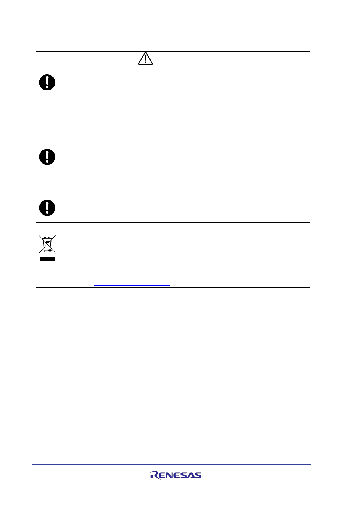
To avoid a possible danger, the following diagrammatic symbols are used to call your attention.
means WARNING or CAUTION.
Example
means PROHIBITION.
Example:
means A FORCIBLE ACTION.
Example:
Precautions for Safety
This chapter describes the precautions which should be taken in order to use this product safely and properly. Be
sure to read and understand this chapter before using this product. Contact your local distributor if you have any
questions about the precautions described here.
WARNING
CAUTION
:
WARNING indicates a potentially dangerous situation that will cause death
or heavy wound unless it is avoided.
CAUTION indicates a potentially dangerous situation that will cause a slight
injury or a medium-degree injury unless it is avoided.
CAUTION AGAINST AN ELECTRIC SHOCK
DISASSEMBLY PROHIBIT ED
UNPLUG THE POWER CABLE FROM THE RECEPTACLE.
R20UT4460EJ0110 Rev. 1.10 Page 6 of 53
Nov. 01, 2019
Page 7
WARNING
Warnings for AC Power Supply:
Do not repair or remodel the emulator product by yourself in order to prevent danger such
Warning for Modification:
Do not modify this produc t. Personal injury due to electric shock may occur if the product
Warning for Installation:
Do not set this product in water or areas of high humidity. Make sure that the product does
Warning for Use Temperature:
This product is to be used in an environment with a maximum ambient temperature of
as an electric shock or fire and for the sake of quality assurance. For after-sale services in
case of a mechanical or electrical fault, please contact your local distributor.
Always switch of f the user system before connecting or disconnecting any connectors or
cables. Neglecting to take this precaution may result in an electric shock or in this product
emitting smoke or catching fire. Also, a us er pr ogram being debugged may be destroyed.
Make sure that the connectors and cables are connected in the correct directions.
Neglect of this precaution will result in getting an electric shock or will result in this product
emitting smoke or catching fire.
is modified. Modifying the product will void your warranty.
not get wet. Spilling water or some other liquid into the product may cause un-repairable
damage.
40°C.
Care should be taken that this temperature is not exceeded.
R20UT4460EJ0110 Rev. 1.10 Page 7 of 53
Nov. 01, 2019
Page 8
CAUTION
Cautions to Be Taken for Handling This Product:
Use caution when handling this product. Be careful not to apply a mechanical shock.
Caution to Be Taken for System Malfunctions:
If this product malfunctions because of interference like external noise, do the following to
Caution to Be Taken for Disposal:
Penalties may be applicable for incorrect disposal of this waste, in accordance with your
European Union Regulatory Notices:
The WEEE (Waste Electrical and Electronic Equipment) regulations put responsibilities on
Do not operate switches before removing static electricity from the operator’s body. Doing
so may lead to the discharge of static electricity and so damage the internal circuits. Also,
do not directly touch connector pins.
When attaching and removing the cable, hold a fixture (such as a connector) to avoid
pulling the cable.
remedy the trouble.
(1) Exit the emulator debugger, and t urn off the emulator and the target system.
(2) After a lapse of 10 seconds, turn on the power of this product again, then launch the
emulator debugger.
national legislation.
producers for the collection and recycling or disposal of electrical and electronic waste.
Return of WEEE under these regulations is applicable in the European Union only. This
equipment (including all accessories) is not intended for household use. After use the
equipment cannot be disposed of as household waste, and the WEEE must be treated,
recycled and disposed of in an environmentally sound manner.
Renesas Electronics Europe GmbH can take back end of life equipment, register for this
service at “
http://www.renesas.eu/weee”.
R20UT4460EJ0110 Rev. 1.10 Page 8 of 53
Nov. 01, 2019
Page 9

Contents
Preface ........................................................................................................................................... 3
Important ....................................................................................................................................... 4
Precautions for Safety ................................................................................................................... 6
Contents ........................................................................................................................................ 9
Terminology ................................................................................................................................ 10
1. Outline ..................................................................................................................................... 11
1.1 Package Components ................................................................................................................................... 11
1.2 Product Specifications.................................................................................................................................. 12
1.3 Regulatory Compliance Notices .................................................................................................................. 13
2. Names and Functions of Hardware ......................................................................................... 15
2.1 Emulation Adapter (RTE7702012EAB00000J) ........................................................................................... 15
2.2 Base Board (RTE7702012EABBB000J) .................................................................................................. 20
2.3 34-Pi n to 14-Pi n Con vers i on A dapt er (RTE0T00020KCA30000J) ............................................................. 25
2.4 Power-Supply Cable .................................................................................................................................... 26
2.5 Demounting Lever ....................................................................................................................................... 27
3. System Configuration and Setup ............................................................................................ 28
3.1 System Configuration as a Simple Evaluation Board .................................................................................. 28
3.2 System Configuration as an Emulation Board ............................................................................................. 33
4. Notes ....................................................................................................................................... 39
4.1 Setting Option Bytes .................................................................................................................................... 39
4.2 Notes on Differences between the Actual Device and the Emulation Adapter ............................................ 39
5. Characteristics of Target Interface .......................................................................................... 41
6. Maintenance and Warranty ..................................................................................................... 42
6.1 Maintenance ................................................................................................................................................. 42
6.2 Warranty ...................................................................................................................................................... 42
6.3 Repair Provisions ......................................................................................................................................... 42
6.4 How to Request Repairs ............................................................................................................................... 43
Appendix A Specifications of the Exchange Adapter ............................................................. 44
Revision History ......................................................................................................................... 50
R20UT4460EJ0110 Rev. 1.10 Page 9 of 53
Nov. 01, 2019
Page 10

Terminology
Some specific words used in this user's manual are defined below.
Target device
This means the device to be emulated or debugged.
Debug chip
This means the device that emulates the operation of the target device and implements debugging facilities such as
tracing.
Aurora tracing
Aurora is a high-speed communications protocol from Xilinx Inc. The debug chip is capable of using Aurora as a
trace interface.
Target system
This means the user-created system whic h is to be debugged. This includes both hardware and software created by
the user.
Emulation adapter
This is a board which emulates the device to be debugged. A debug chip is mounted on the board.
Base board
This board is for operating the emulation adapter as a stand-alone unit.
Exchange adapter
This is a board that exchanges the connections of the emulation adapter to suit the package of the target device.
R20UT4460EJ0110 Rev. 1.10 Page 10 of 53
Nov. 01, 2019
Page 11
Emulation Adapter Outline
1. Outline
This product is an emulation adapter for the RH850/E2UH and E2H groups of MCUs from Renesas Electronics
Corporation. Using this product with the separately sold exchange adapter enables emulation of the target device.
Features:
• This product includes a debug chip (R7F702Z10AADBG) for the RH850/E2UH and E2H groups.
• The combination of the emulation adapter connected to the base board included in the package is usabl e as a
simple evaluation board.
• Using the emulation adapter with the exchange adapter allows connection to the target system and enables
emulation of the target device.
• Connecting an emulator which supports Aurora tracing, such as the IE850A emulator (type name:
RTE0T0850AKCT00000J) from Renesas, enables debugging.
• Using the attached 34-pin to 14-pin conversion connector enables connecting the emulation adapter to on-chip
debugging emulators and flash programmers, such as the E2 emulator (type name: RTE0T00020KCE00000R)
from Renesas.
• The emulation adapter can operate as a stand-alone unit, i.e. without connection t o an emulator.
1.1 Package Components
The package of this product consists of the following items. After you have unpacked the box, check if your
emulation adapter contains all of these items.
Table 1-1 Package Components for the Emulation Adapter
Item Quantity
Emulation adapter: RTE7702012EAB00000J 1
Base board: RTE7702012EABBB000J 1
34-pin to 14-pin conversion adapter: RTE0T00020KCA30000J 1
Power-supply cable 1
Demounting lever 1
Jumper blocks for pin headers 5
R20UT4460EJ0110 Rev. 1.10 Page 11 of 53
Nov. 01, 2019
Page 12
Emulation Adapter Outline
Item
Specification
Device to be emulated
468-pin BGA: RH850/E2UH
External dimension
Emulation adapter: 47 mm x 51 mm
Operating temperature
0 to 40°C (no condensation)
EMC
EU: EN55032 Class A, EN55024
1.2 Product Specifications
Table 1-2 lists the specifications of this product.
Table 1-2 Product Spe cifications
468-pin BGA: RH850/E2H
373-pin BGA: RH850/E2H
Power supply for the emulation adapter 4.5 V min., 5.0 V typ., 5.5 V max.
Base board: 100 mm x 120 mm
Weight Emulation adapter: 22 g
Base board: 79 g
Storage temperature −15 to 60°C (no condensation)
USA: FCC part 15 Class A
R20UT4460EJ0110 Rev. 1.10 Page 12 of 53
Nov. 01, 2019
Page 13

Emulation Adapter Outline
WARNING: This is a Class A product. This equipment can cause radio frequency noise when used
1.3 Regulatory Compliance Notices
• European Union regulatory notices
This product complies with the following EU Directives. (These directives are only valid in the European
Union.)
CE Certifications:
This product complies with the following European EMC standards.
• EMC Directive (2014/30/EU)
EN 55032 Class A
in the residential area. In such cases, the user/operator of the equipment may be
requ ir ed to take a ppropriate countermeasures under his responsibility.
EN 55024
Information for traceability:
• Authorised representative & Manufacturer
Name: Renesas Electronics Corporation
Address:
• Person responsible for placing on the market
Name: Renesas Electronics Europe GmbH
Address: Arcadiastrasse 10, 40472 Dusseldorf, Germany
• Trademark and Type name
Trademark: Renesas
TOYOSU FORESIA, 3-2-24, Toyosu, Koto-ku, Tokyo, 135-0061, Japan
Product name: RH850/E2x-FCC2 Emulation adapter + Bas e board
Type name: RTE7702012EAB00000J
Environmental Compliance and Certifications:
• Waste Electrical and Electronic Equip ment (W EE E) Direc tiv e 201 2/1 9/EU
• United States Regulatory notices on Electromagnetic compatibility
This product complies with the following EMC regulation. (This is only valid in the United States.)
R20UT4460EJ0110 Rev. 1.10 Page 13 of 53
Nov. 01, 2019
Page 14

Emulation Adapter Outline
CAUTION: Changes or modifications not expressly approved by the party responsible for
FCC Certifications:
This equipment has been tested and found to comply with the limits for a Class A digital device,
pursuant to Part 15 of the FCC Rules. These limits are designed to provide reasonable protection
against harmful interference when the equipment is operated in a commercial environment. This
equipment generates, uses, and can radiate radio frequency energy and, if not installed and used in
accordance with the instruction manual, may cause harmful interference to radio communications.
Operation of this equipment in a residential area is likely to cause harmful interference in which case
the user will be required to correct the interference at his own expense.
This device complies with Part 15 of the FCC Rules. Operation is subject to the following two
conditions: (1) this device may not cause harmful interference, and (2) this device must accept any
interference received, including interference that may cause undesired operation.
compliance could void the user's authority to operate the equipment.
R20UT4460EJ0110 Rev. 1.10 Page 14 of 53
Nov. 01, 2019
Page 15
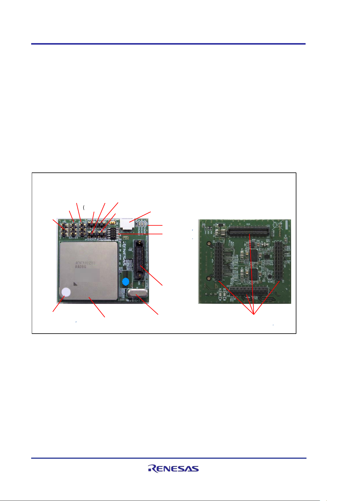
Emulation Adapter Names and Functions of Hardwar e
(7) JP5
(10) LED
(3) CN2
2. Names and Functions of Hardware
This chapter describes the names and functions of each part of the emulation adapter and of the other items
included with it. You can avoid damaging the product and affecting the system by reading this chapter with
reference to the actual hardware.
Chapter 3 shows a list of the settings of hardware according to the system configuration (type of usage).
2.1 Emulation Adapter (RTE7702012EAB00000J)
An emulation adapter is an emulation board on which the debug chip is mounted. Using the emulation adapter
with the exchange adapter allows connection to the target system. The emulation adapter can also be used as a
simple evaluation board in combination with the attached base board.
(9) JP7
(13) Pin 1
Top view
(7) JP4
(8) JP6
Figure 2-1 Names of the Parts of the Emula tion Adapter (RTE7702012EAB00000J)
(6) JP3
(1) IC1
(5) JP1
(5) JP2
(12) JP8
(2) CN1
(4) X1
(11) Interfaces for the exchange
adapter
Bottom view
(1) Debug chi p: IC1
IC1 is the debug chip (R7F702Z10AADBG), which can emulate target devices of the RH850/E2UH and E2H
groups.
R20UT4460EJ0110 Rev. 1.10 Page 15 of 53
Nov. 01, 2019
Page 16
Emulation Adapter Names and Functions of Hardwar e
TODP0
1 2 TVCC (VCC)
GND
5 6 TMS
TODN1
9
10
TDO
TODP2
13
14
MD0
GND
17
18
EVTO
TODN3
21
22
RESET
MSYNZ
25
26
CICREFP
GND
29
30
GND
(BGNT)
33
34
RESOUT
(2) Connector for external tracing: CN1
CN1 is a connector for connection to emulators which support Aurora tracing, such as the IE850A emulator (type
name: RTE0T0850AKCT00000J) f rom Renesas.
CN1 is a 34-pin connector from SAMTEC, the type name of which is ASP-137973-01. The table below lists the
pin assignments.
Read the user's manual for the emulator you will be using and connect the emulator with this connector.
Table 2-1 Pin Assignments of the Connector for External Tracing
Signal Name Pin No. Pin No. Signal Name
TODN0 3 4 TCK
TODP1 7 8 TDI
GND 11 12 TRST
TODN2 15 16 EVTI
TODP3 19 20 MD1
GND 23 24 GND
(WDTDIS) 27 28 CICREFN
(BREQ) 31 32 DRDY
(3) Power-supply connector: CN2
CN2 is connected to the power-supply cable that comes with this product or that come s with the IE850A. When a
base board is connected and emulation RAM (ERAM) or external tracing (Aurora tracing) is used, be sure to
connect the power-supply cable to CN2 and supply +5 V.
When disconnecting the power-supply cable from the emulation adapter, press the tabs on both sides of the CN1
connector of the power-supply cable to unlock the connector.
CAUTION
Applied voltage:
Make sure that the voltage applied to CN2 is within the specified range (4.5 V to 5.5 V).
An applied voltage out of the range may cause the emulation adapter to emit smoke or
catch fire or otherwise be damaged.
R20UT4460EJ0110 Rev. 1.10 Page 16 of 53
Nov. 01, 2019
Page 17

Emulation Adapter Names and Functions of Hardwar e
Unlocking the connector:
Open-circuit
Open-circuit
400-MHz mode
Short-circuit
Open-circuit
Open-circuit
ICE pin = low
CAUTION
Do not press the tabs for unlocking the connector too hard as this may lead to them being
stuck in this position. Take care on this point.
(4) Clock sock et: X1
X1 is the socket for the main oscillator. A 40-MHz oscillator is mounted upon the board as shipped.
Taking the oscillation characteristics into consideration, an oscillator on the target system is not used; the
oscillator in this soc ket is used instead. Change the oscillator in the socket if this is required.
(5) Jumper blocks: JP2 (CLGMD1) and JP1 (CLGMD0)
JP2 (CLGMD1) JP1 (CLGMD0) Specification
(default)
Open-circuit Short-circuit
Short-circuit Short-circuit
(default)
(6) Jumper block: JP3 (ICE)
JP3 (ICE) Specification
(default)
Short-circuit ICE pin = high
Security settings in the debug chip are enabled.
Security settings in the debug chip are partially disabled.
Settings prohibited.
R20UT4460EJ0110 Rev. 1.10 Page 17 of 53
Nov. 01, 2019
Page 18

Emulation Adapter Names and Functions of Hardwar e
JP6 (AURORES)
Specification
1-2 short-circuit
The AURORES pin is operated by the TRST pin.
Open-circuit
Setting prohibited.
2-3 short-circuit
VDD on the target system is supplied as VDD for the debug chip.
JP4 (EMUVCC)
JP5 (EMUVDD)
Specification
Open-circuit
1-2 short-circuit
Setting prohibited.
Short-circuit
Open-circuit
Setting prohibited.
Short-circuit
2-3 short-circuit
Setting prohibited.
(7) Jumper blocks: JP4 (EMUVCC) and JP5 (EMUVDD)
Open-circuit Open-circuit Setting prohibited.
EMUVCC = OFF, EMUVDD = always ON
EMUVCC = OFF, EMUVDD = ON: Operation is with VCC.
Open-circuit 2-3 short-circuit EMUVCC = OFF, EMUVDD = OFF
This setting is enabled when neither ERAM nor external
tracing (Aurora tracing) is to be used.
At the same time, make JP6 (AURORES) open-circuit.
EMUVCC = ON, EMUVDD = always ON
Short-circuit
(default)
1-2 short-circuit
(default)
EMUVCC = ON, EMUVDD = ON: Operation is with VCC.
This setting must be made when ERAM or external tracing
(Aurora tracing) is to be used.
At the same time, make 1-2 on JP6 (AURORES) short-
circuit.
EMUVCC = ON, EMUVDD = OFF
(8) Jumper block: JP6 (AURORES)
Open-circuit AURORES pin = low
This setting is made when external tracing (Aurora tracing) is not to be used.
(default)
2-3 short-circuit Setting prohibited.
Check that the setting is consistent with the form of operatio n selec ted by JP4 and JP5.
When the emulator is connected, the level on the pin changes from low to high.
AURORES pin = high
(9) Jumper block: JP7 (VDD)
JP7 (VDD) Specification
1-2 short-circuit
(default)
The power generated on the emulation adapter is supplied as VDD for the debug
chip.
This setting must be made when the emulation adapter is to be connected to the
base board.
When this setting is to be used, refer to notes in section 4.2.3.
R20UT4460EJ0110 Rev. 1.10 Page 18 of 53
Nov. 01, 2019
Page 19

Emulation Adapter Names and Functions of Hardwar e
POWER
Illuminated: CN2 is supplying power.
EMUVDD
Illuminated: EMUVDD = ON
(10) Status LEDs
Name of LED Specification
Not illuminated: CN2 is not supplying pow er.
EMUVCC Illuminated: EMUVCC = ON
Not illuminated: EMUVCC = OFF
Not illuminated: EMUVDD = OFF
(11) Interfaces for the exchange adapter: CN10, CN11, CN12, and CN13
These connectors are used to connect an exchange adapter or the base board. CN10 has a different shape from the
others to prevent erroneous insertion.
(12) Pin he ader: JP8
JP8 is a pin header for the AUD-R pin.
(13) Sticker for aligning the position of pin 1
This mark indicates the position of pin 1 in the pad pattern for the device to be emulated on the target system.
R20UT4460EJ0110 Rev. 1.10 Page 19 of 53
Nov. 01, 2019
Page 20

Emulation Adapter Names and Functions of Hardwar e
Top view
(2) SW1
(8) Pin 1
(9) CN1 CN2
(9) CN5 CN6
JP12
2.2 Base Board (RTE7702012EABBB000J)
The base board allows use as a simple target system in combination with the emulation adapter.
The signals to or from each pin of the debug chip are brought out on CN1 to CN8 on the board, which enables
simple checking.
(9) CN7 CN8
(9) CN4 CN3
(1) Interfaces
for the
exchange
adapter
(6) JP17
(7) JP18
(3) SW2
(5) JP1 JP2 JP3 JP4 JP5 JP6 JP7 JP8 JP9 JP10 JP11
(4) LED
(5)
JP16
JP15
JP14
JP13
Figure 2-2 Nam es of the Parts of the Base Boa rd (RTE7702012EABBB000J)
(1) Interfaces for the exchange adapter: CN10, CN11, CN12, and CN13
These connectors are used for connection to the emulation adapter. CN10 has a different shape from the others to
prevent erroneous insertion. These connectors are connected to CN10, CN11, CN12, and CN13 of the emulation
adapter.
R20UT4460EJ0110 Rev. 1.10 Page 20 of 53
Nov. 01, 2019
Page 21

Emulation Adapter Names and Functions of Hardwar e
ON
This switch turns on the power supply of the base board.
Operating the switch:
Do not operate a switch before removing static electricity from the operator’s body . Doing
SW2 (RESET SW)
Specification
H
Reset released state.
Reset state.
(2) Switch: SW1 (POWER SW)
SW1 (POWER SW) Specification
(default)
OFF
so may lead to the discharge of static electricity and so damage the internal circuits.
(3) Switch: SW2 (RESET SW)
Turn this switch on after connecting the emulation adapter and starting the
supply of power from CN2 of the emulation adapter.
This switch turns off the power supply of the base board.
CAUTION
(L)
(default)
L
This position starts release from the reset state after the debug chip has been
reset.
The switch returns to the “H” position a moment after it stops being pressed.
The state of the reset pin of the debug chip changes from “L” to “H” (pulled up).
The reset pin of the debug chip is in the “H” (pulled up) state.
The reset pin of the debug chip is in the “L” state.
R20UT4460EJ0110 Rev. 1.10 Page 21 of 53
Nov. 01, 2019
Page 22

Emulation Adapter Names and Functions of Hardwar e
Operating the switch:
Do not operate a switch before removing static electricity from the operator’s body. Doing
LED2 (5 V)
Illuminated: The 5-V power supply on the base board is on.
JP
Target Power-Supply Voltage
JP2
ADSVRFFH
JP4
A1VCC
JP6
A3VCC
JP8
A1VREFFH
JP10
A3VREFFH
JP12
E1VCC
JP14
LVDVCC
JP16
VCC
JP1 to JP11
Specification
CAUTION
so may lead to the discharge of static electricity and so damage the internal circuits.
(4) Status LEDs: LED1 (3.3 V) and LED2 (5 V)
Name of LED Specification
LED1 (3.3 V) Illuminated: The 3.3-V power supply on the base board is on.
Not illuminated: The 3.3-V power supply on the base board is off.
Not illuminated: The 5-V power supply on the base board is off.
(5) Jumper blocks: JP1 to JP16 (selecting each of the power-supply voltages)
The target power-supply voltages for each of these jumper blocks are listed below.
JP1 ADSVCC
JP3 A0VCC
JP5 A2VCC
JP7 A0VREFFH
JP9 A2VREFFH
JP11 E0VCC
JP13 E2VCC
JP15 SYSVCC
Each jumper block has common specifications as shown in the following table.
Open-circuit The target power-supply voltage is off.
1-2 short-circuit
(default)
5 V is supplied as the target power-supply voltage.
R20UT4460EJ0110 Rev. 1.10 Page 22 of 53
Nov. 01, 2019
Page 23

Emulation Adapter Names and Functions of Hardwar e
Open-circuit
The target power-supply voltage is off.
1-2 short-circuit
5 V is supplied as the target power-supply voltage.
JP17 (MD0)
Specification
Open-circuit
MD0 pin = “L” (pulled down)
JP18 (MD1)
Specification
Open-circuit
MD1 pin = “L” (pulled down)
Each jumper block has common specifications as shown in the following table.
JP12 to JP16 Specification
(default)
2-3 short-circuit 3.3 V is supplied as the target power-supply voltage.
(6) Jumper block: JP17 (MD0)
(default)
Short-circuit MD0 pin = “H” (pulled up)
(7) Jumper block: JP18 (MD1)
(default)
Short-circuit MD1 pin = “H” (pulled up)
(8) Silk-screened mark for aligning the position of pin 1
When connecting the emulation adapter, match the position of the sticker for aligning the position of pin 1 on the
emulation adapter with that of the silk-screened mark for aligning the position of pin 1 on the base board.
R20UT4460EJ0110 Rev. 1.10 Page 23 of 53
Nov. 01, 2019
Page 24

Emulation Adapter Names and Functions of Hardwar e
1
2 3 4 5 6 7 8 9 10 11 12 13 14 15 16 17 18 19 20 21 22 23 24 25 26 27 28 29 30
GNDP02_5P02_4P02_1P10
_11
P10
_10
P10_5P10_4P13
_14
P13
_13
P13_8P13_7P13_2P11
_10
P11_9P11_4P11_3P11_0P12_7P12_4P12_1P14
_11
P14_6P14_5P14_0P15_8P15_3P15_0P24
_15
P24
_12
GNDP02_6P02_3P02_0P10
_12
P10_9P10_6P10_3P10_0P13
_12
P13_9P13_6P13_3P13_0P11_8P11_5P11_2P12_9P12_6P12_3P12_0P14
_10
P14_7P14_4P14_1P15_7P15_4P15_1P24
_14
P24
_11
GNDP02_7P02_2P10
_14
P10
_13
P10_8P10_7P10_2P10_1P13
_11
P13
_10
P13_5P13_4P13_1P11_7P11_6P11_1P12_8P12_5P12_2P14
_12
P14_9P14_8P14_3P14_2P15_6P15_5P15_2P24
_13
P24
_10
30 GND
GND
GND GND GND GND 1
29
P02_10
P02_9 P02_8
P20_7 P20_6 P20_5 2
28 P02_11
P01_15 P01_14 P20_2 P20_3 P20_4 3
27 P01_11 P01_12 P01_13
P20_1 P20_0
ERRORO
UT M
4
26 P01_10
P01_9 P01_8 P24_9
RES_IN
RES_OU
5
25 P01_5
P01_6 P01_7
P24_8 P24_7 P24_6 6
24 P00_0 P01_4 P01_3 P24_3 P24_4 P 24_5 7
23 P00_1 P00_2 P00_3
P24_2 P24_1 P24_0 8
22
P00_4
P00_5
P00_6
P21_3 P21_4 P21_5 9
21 P00_7 P00_8
P00_9
P21_2 P22_13 P22_12 10
20 AN373 P00_10 P00_11 P22_9 P22_10 P22_11 11
19 AN372 AN371 AN370
P22_8 P22_7 P22_6 12
18 AN303
AN302
AN301
P22_3 P22_4 P22_5 13
17 AN313 AN312 AN300
P22_2 P22_1 P22_0 14
16 AN323 AN311 AN310
NC NC NMI 15
15 AN322 AN321 AN320 NC GND GND 16
14
AN363
AN362
AN361 P23_5 P23_6 P23_7 17
13 AN353 AN352 AN360 P23_4 P23_3 P23_2 18
12
AN273 AN351 AN350
P25_0 P23_0 P23_1 19
11 AN272 AN271
AN270 P25_1 P25_2 P25_3 20
10 AN263
AN262 AN261 P25_6 P25_5 P25_4 21
9 AN253
AN252 AN260 P25_7 P25_8 P25_9 22
8 AN233 AN251
AN250 P25_12 P25_11 P25_10 23
7 AN232 AN231 AN230 P25_13 P25_14 P25_15 24
6
AN223 AN222
AN221 P26_0 P26_1 P31_15 25
5 AN243
AN242 AN220 P31_12 P31_13 P31_14 26
4 AN203
AN241 AN240 P31_11 P31_10 P31_9 27
3 AN202 AN201 AN200
P31_6 P31_7 P31_8 28
2 AN211 AN212 AN213
P31_5 P31_4 P31_3 29
1 AN210
GND
GND P31_0 P31_1 P31_2 30
GNDAN
031AN030AN010AN000AN021AN020AN040AN051AN050AN060AN120AN111AN110AN100
P34_3P34_4P33_3P33_4P33_9P33
_10
P32_1P32_2P32_6P30_3P30_4P30_9P30
_10
P30
_15
GN
D
GNDAN
032AN012AN011AN001AN022
NC
AN
041AN053AN062AN061AN121AN112AN102AN101
P34_2GNDP33_2P33_5P33_8P33
_11
P32_0P32_3P32_5P30_2P30_5P30_8P30
_11
P30
_14GND
GNDAN
033AN013AN003AN002AN023AN043AN042AN052AN063AN123
AN
122AN113
AN
103
P34_0P34_1P33_0P33_1P33_6P33_7P33
_12
P33
_13
P32_4P30_0P30_1P30_6P30_7P30
_12
P30
_13
GN
D
30 29 28
27 26 25 24 23 22 21 20 19 18 17 16 15 14 13 12 11 10 9 8 7 6 5 4 3 2 1
CN4
CN3
CN2
CN1
CN7
CN8
CN5
CN6
(9) Pin heade rs for controlling a nd monitoring the pins of the debug chip (CN1 to CN8)
Figure 2-3 shows the assignment of pin headers for each pin of the debug chip.
Figure 2-3 Assignment of Pin Headers
R20UT4460EJ0110 Rev. 1.10 Page 24 of 53
Nov. 01, 2019
Page 25

Emulation Adapter Names and Functions of Hardware
Signal Name
Pin No.
Pin No.
Signal Name
TRST
3 4 FPMD0 (MD0)
TDI/LPDIO
7 8 TVDD (VCC)
DRDY/LPDCLKO
11
12
GND
Bottom view
Top view
(2) CN2
(1) CN1
Side view
2.3 34-Pin to 14-Pin Conversion Adapter (RTE0T00020KCA30000J)
The conversion adapter is an adapter board that is used to connect an emulator with a 14-pin connector to the
emulation adapter and is required for debugging in such situations.
Figure 2-4 Names of the Parts of the 34-Pin to 14-Pin Conversion Ada pter (RTE0T00020KCA30000J)
(1) Connector: CN1 (34-pin side)
CN1 can be connected to CN1 for external tracing through the emulation adapter.
(2) Connector: CN2 (14-pin side)
CN2 is a 14-pin connector that is defined as a connector for the RH850 emulators. This connector can be
connected to on-chip debugging emulators such as the E2 emulator (type name: RTE0T00020KCE00000R) from
Renesas and flash programmers that support the 14-pin connector.
The following shows pin assignments of CN2. Read the user's manual for the emulator you will be using and
connect the emulator with this connector.
Table 2-2 Pin Assignments of the 14-Pin Connect or (CN2)
TCK/LPDCLK 1 2 GND
TDO/LPDO 5 6 FPMD1 (MD1)
TMS 9 10 EVTO
RESET 13 14 GND
R20UT4460EJ0110 Rev. 1.10 Page 25 of 53
Nov. 01, 2019
Page 26

Emulation Adapter Names and Functions of Hardwar e
Unlocking the connector:
Do not press the tabs for unlocking the connector too hard as this may lead to them being
(1) CN1
2.4 Power-Supply Cable
The power-supply cable (about 300-mm long) supplies power to the emulation adapter.
(3) J2
(4) Tabs for unlocking the
connector
(2) J1
Figure 2-5 Names of the Parts of the Power-Supply Cable
(1) Connector: CN1
CN1 is a connector (LEAR-02V-S from JST) for connection to CN2 of the emulation adapter.
(2) Power jack: J1 (red)
Supply 5 V from a stabilized power supply.
(3) Power jack: J2 (black)
Connect J2 to GND.
(4) Tabs fo r unlocking the connector
When disconnecting the power-supply cable from the emulation adapter, press the tabs on both sides of the CN1
connector of the power-supply cable to unlock the connector.
CAUTION
stuck in this position. Take care on this point.
R20UT4460EJ0110 Rev. 1.10 Page 26 of 53
Nov. 01, 2019
Page 27

Emulation Adapter Names and Functions of Hardwar e
Side view
Top view
The four positions for applying the demounting lever
2.5 Demounting Lever
The demounting lever which comes with this product is used to remove the emulation adapter from the base board
or exchange adapter.
To remove the emulation adapter from the base board or exchange adapter, insert the demounting lever alternately
below all four corners of the emulation adapter and gradually pull the emulation adapter out.
Point for caution on removing the emulation adapter:
When you remove the emulation adapter from the base board or exchange adapter, take
care not to damage or deform peripheral components.
R20UT4460EJ0110 Rev. 1.10 Page 27 of 53
Nov. 01, 2019
Figure 2-6 De mounting Lever
CAUTION
Page 28

Emulation Adapter System Configurati on and Set up
3. System Configuration and Setup
The system configurations of this emulation adapter are as follows according to your intentions in using it.
• A simple evaluation board (See section 3.1.)
• An emulation board (See section 3.2.)
3.1 System Configuration as a Simple Evaluation Board
Figure 3-1 shows a system configuration when the emulation adapter is connected to the base board for use as a
simple evaluation board. Connection of an emulator is not essential.
Using the pin headers on the base board enables the control and monitoring of each pin of the target device.
Figure 3-1 System Configuration (Simple Evaluation Board)
R20UT4460EJ0110 Rev. 1.10 Page 28 of 53
Nov. 01, 2019
Page 29

Emulation Adapter System Configuration and Setup
Item
Description
Connector for external tracing:
When an emulator is in use: Connect the cable for the emulator or the 34-
Power-supply connector: CN2
Set up a +5-V supply through the attached power-supply cable.
Jumper blocks: JP2 (CLGMD1)
We recommend making JP2 and JP1 open-circuit. Refer to (5) in sec tion
Jumper blocks: JP4 (EMUVCC)
We recommend making JP4 and 1-2 on JP5 short-circuit. Refer to (7) in
Jumper block: JP7 (VDD)
Be sure to make 1-2 on JP7 short-circuit. Refer to (9) in section 2.1.
Interfaces for the exchange
Interfaces for the exchange
Connect these connectors to the emulation adapter.
Switch: SW2 (RESET SW)
Refer to (3) in sect ion 2.2.
Jumper block: JP17 (MD0)
We recommend making JP17 open-circuit. Refer to (6) in section 2.2.
3.1.1 Settings for Use as a Simple Evaluation Board
Table 3-1 and Table 3-2 show lists of the recommended settings for this system configuration.
Table 3-1 Settings for Use as a Simple Evaluation Board (Emulation Ada pter)
Debug chip: IC1 Se t an option byte. Refer to section 4.1.
CN1
Clock socket: X1 An oscillator is mounted (40 MHz at shipment).
and JP1 (CLGMD0)
Jumper block: JP3 (ICE) We recommend making JP3 open-circuit. Refer to (6) in section 2.1.
and JP5 (EMUVDD)
Jumper block: JP6 (AURORES) We recommend making 1-2 on JP6 short-circuit. Refer to (8) in section 2.1.
adapter: CN10, CN11, CN12, and
CN13
pin to 14-pin conversion adapt er.
When an emulator is not in use: Leave the connector open-circuit.
If you are using the IE850A, power can be supplied from the power-supply
cable attached to the IE850A.
When you are evaluating the emulation adapter with a main oscillator that
has a different frequency (e.g. 20 MHz), change the oscillator.
2.1.
section 2.1.
Connect these connectors to the base board.
Table 3-2 Settings for Use as a Simple Evaluation Board (Base Board)
Item Description
adapter: CN10, CN11, CN12, and
CN13
Switch: SW1 (POWER SW) Refer to (2) in sect ion 2.2.
Jumper blocks: JP1 to JP16
(selecting each of the powersupply voltages)
Jumper block: JP18 (MD1) We recommend making JP18 open-circuit. Refer to (7) in section 2.2.
The voltage of each power supply is selected according to the conditions
to be evaluated or the specifications of the target device. Refer to (5) in
section 2.2.
R20UT4460EJ0110 Rev. 1.10 Page 29 of 53
Nov. 01, 2019
Page 30

Emulation Adapter System Configurati on and Set up
3.1.2 Procedure for Setting the Emulation Adapter up as a Simple Evaluation Board
This section describes the procedure for setting the emulation adapter up for use as a simple evaluation board.
(1) Settings on the boards
Make settings for the emulation adapter and base board according to the statements in section 3.1.1. Turn off the
SW1 switch (PO WER SW) on the base board and set the SW2 switch (RESET SW) for the low level.
(2) Connecting the power-supply cable
Connect the power-supply cable which comes with this product to the CN2 power-supply connect or of the
emulation adapter then connect a power-supply unit such as a stabilized power supply. Do not turn the power on.
If you are using an IE850A emulator, power can be supplied by connecting the power-supply cable attached to the
IE850A.
(3) Connecting the emulation ada pter to the base board
Connect the two boards so that the sticker and silk -screened mark for aligning the positions of pin 1 of the
emulation adapter and base board are in the same position.
(4) Connecting the emulator (o nly if you are using an emulator)
Connect the emulator to the CN1 connector for external tracing from the emulation adapter. If you are using an
emulator (e.g. an IE850A) that supports external tracing (Aurora tracing), directly connect the emulator cable. If
you are using an emulator (e.g. an E2) that supports a 14-pin connector, connect the emulator via the 32-pin to 14pin conversion adapter.
CAUTION
Connecting the emulator:
Confirm the directio n with the notch on the connector and con nect the e mulator while taking
care that the direction of insertion is correct.
(5) Turning on the emulator (o nly if you are using an emulator)
Turn on the emulator. For details, refer to the manuals for the emulator you are using.
R20UT4460EJ0110 Rev. 1.10 Page 30 of 53
Nov. 01, 2019
Page 31

Emulation Adapter System Configurati on and Set up
(6) Turning on the emulation adapter and base board and releasing a reset
Output 5 V from the power-supply unit that is connected to the power-supply connector (CN2) of the emulation
adapter and turn the switch (SW1; POWER SW) of the base board on. Then, set SW2 (RESET SW) for the high
level.
Accordingly, if an emulator is not connected, the debug chip will start executing a program.
When the emulator is connected, the debug chip will be kept in the reset state before execution of a program is
started by the debugger after the debugger has been launched, although this depends on the specifications of the
emulator.
CAUTION
Applied voltage:
Make sure that the voltage applied to CN2 is within the specified range (4.5 V to 5.5 V).
An applied voltage out of the range may cause the emulation adapter to emit smoke or
catch fire or otherwise be damaged.
(7) Launching the debugger (only if you are using an emulator)
Launch the debugger to start debugging. The first time this is done, an option byte must be set according to the
target device to be emulated.
R20UT4460EJ0110 Rev. 1.10 Page 31 of 53
Nov. 01, 2019
Page 32

Emulation Adapter System Configurati on and Set up
Unlocking the connector:
Do not press the tabs for unlocking the connector too hard as this may lead to them being
3.1.3 Procedure for Closing a Session of Use as a Simple Evaluation Board
This section describes the procedure for closing a sessio n of using the emulation adapter as a simple evaluation
board.
(1) Closing the debugger (only if you are using an emulator)
Close the debugger.
(2) Turning off and resetting the emulation adapt e r and base board
Set SW2 (RESET SW) of the base board for the low level. Turn the switch (SW1; POWER SW) of the base board
off. Turn off the output from the power-supply unit that is connected to the power-supply connector (CN2) of the
emulation adapter.
(3) Turning off the emulator (only if you are using an emulator)
Turn off the emulator. For details, refer to manuals for the emulator you are using.
Take the steps below as required.
(4) Disconnec ting the emulator (only if you are using an emulator)
Disconnect the emulator from the emulation adapter.
(5) Disconnec ting the emulation adapter from the base board
To disconnect the emulation adapter from the base board, insert the demounting lever which comes with this
product into alternate corners among the four corners between the two boards and gradually p ull the emulation
adapter out. Take care of the positions where you insert the demounting lever so that you do not accidentally tear
off components on the boards. For details, refer to section 2.5.
(6) Disconnecting the power-supply cable
Disconnect the power-supply cable from the CN2 power-supply connector of the emulation adapter. When
disconnecting the power-supply cable from the emulation adapter, press the tabs on both sides of the CN1
connector of the power-supply cable to unlock the connector.
CAUTION
stuck in this position. Take care on this point.
R20UT4460EJ0110 Rev. 1.10 Page 32 of 53
Nov. 01, 2019
Page 33

Emulation Adapter System Configurati on and Set up
3.2 System Configuration as an Emulation Board
Figure 3-2 shows a system configuration when the emulation adapter is to be connected to the exchange adapter
then connected to a target board (the base board is not used). For the specifications of the exchange adapter, refer
to appendix A, Specifications of the Exchange Adapter.
Figure 3-2 System Configuration ( Emulation Board)
R20UT4460EJ0110 Rev. 1.10 Page 33 of 53
Nov. 01, 2019
Page 34

Emulation Adapter System Configurati on and Set up
Package
Exchange Adapter
Target Connector
Space Adapter
Mount Adapter
3.2.1 List of Exchange Adapters and Sockets
Table 3-3 lists the exchange adapters and sockets for the target devices. They are sold separately from this
product. For the BGA packages, the BSSOCKET target connectors, CSSOCKET space adapters, and LSPACK
mounting adapters can be purchased from Tokyo Eletech Corporation. The exchange adapters can be purchased
from Renesas Electronics Corporation. If you particularly require details on the CSSOCKET space adapter,
contact Tokyo Eletech Corporation.
Table 3-3 Exchange Adapt e rs and Sockets
Device
BGA468
RH850/E2UH
RH850/E2H
BGA373
RH850/E2H
RTE7702012CBG468T000J BSSOCKET468A3025RE21N CSSOCKET468A3025RE03
CSSOCKET468A3025RE04
RTE7702011CBG373T000J BSSOCKET373A2521RE21N CSSOCKET373A2521RE03
CSSOCKET373A2521RE04
LSPACK468A3025RE01
LSPACK373A2521RE01
BSSOCKET target connector (required for emulation):
This connector is for mounting on the target system.
Exchange adapter (required for emulation):
This conversion adapter is for connecting the emulation adapter to the target connector.
CSSOCKET space adapter (optional):
This adapter is used to adjust the height. It is an optional product which is available for use if the components
around the target connector would otherwise touch the exchange adapter or emulation adapter.
LSPACK mount adapter (optional):
When the target device is mounted on the target connector, this adapter is required as a cover.
R20UT4460EJ0110 Rev. 1.10 Page 34 of 53
Nov. 01, 2019
Page 35

Emulation Adapter System Configurati on and Set up
Item
Description
Connector for external tracing:
When an emulator is in use: Connect the cable for the emulator or the 34-
Power-supply connector: CN2
Set up a +5-V supply through the attached power-supply cable.
Jumper blocks: JP2 (CLGMD1)
We recommend making JP2 and JP1 open-circuit. Refer to (5) i n sect ion
Jumper blocks: JP4 (EMUVCC)
We recommend making JP4 and 1-2 on JP5 short-circuit. Refer to (7) in
Jumper block: JP7 (VDD)
We recommend making 1-2 on JP7 short-circuit. R efer to (9) in section 2.1.
Interfaces for the exchange
3.2.2 Settings for Use as an Emulation Board
Table 3-4 and Table 3-5 show lists of the recommended settings of the emulation adapter in this system
configuration. For the settings when the power is supplied from CN2, refer to Table 3-4. If the power is not
supplied from CN2, the settings in Table 3-5 are also required. When you select a configuration in which the
power is not supplied from CN2, note that neither ERAM nor external tracing (Aurora tracing) is available.
Table 3-4 Settings for Use as an Emulation Board when the Power is to be Supplied from CN2
Debug chip: IC1 Set an option byte. Refer to section 4.1.
CN1
Clock socket: X1 An oscillator is mounted (40 MHz at shipment).
and JP1 (CLGMD0)
Jumper block: JP3 (ICE) We recommend making JP3 open-circuit. Refer to (6) in section 2.1.
and JP5 (EMUVDD)
Jumper block: JP6 (AURORES) We recommend making 1-2 on JP6 short-circuit. Refer t o (8) in section 2.1.
adapter: CN10, CN11, CN12, and
CN13
pin to 14-pin conversion adapt er.
When an emulator is not in use: Leave the connector open-circuit.
If you are using the IE850A, p ower can be supp lie d from th e power-supply
cable attached to the IE850A.
When you are evaluating the emulation adapter with a main os c il l at o r t h at
has a different frequency (e.g. 20 MHz), change the oscillator.
2.1.
section 2.1.
Connect these connectors to the exchange adapter.
R20UT4460EJ0110 Rev. 1.10 Page 35 of 53
Nov. 01, 2019
Page 36

Emulation Adapter System Configurati on and Set up
Debug chip: IC1
Set an option byte. Refer to sectio n 4.1.
When an emulator is not in use: Leave the connector open-circuit.
Clock socket: X1
An oscillator is mounted (40 MHz at shipment).
Jumper block: JP3 (ICE)
We recommend making JP3 open-circuit. Refer to (6) in section 2.1.
Jumper block: JP6 (AURORES)
Be sure to make JP6 open-circuit. Refer to (8) in section 2.1.
Interfaces for the exchange
Connect these connectors to the exchange adapter.
Table 3-5 Settings for Use as a n Emulation Board when the Power is not to be Supplied f r om CN2
Item Description
Connector for external tracing:
CN1
Power-supply connector: CN2 Leave the connector open-circuit.
Jumper blocks: JP2 (CLGMD1)
and JP1 (CLGMD0)
Jumper blocks: JP4 (EMUVCC)
and JP5 (EMUVDD)
Jumper block: JP7 (VDD) Be sure to make 2-3 on JP7 short-circuit. Refer to (9) in section 2.1.
adapter: CN10, CN11, CN12, and
CN13
When an emulator is in use: Connect the cable for the emulator or the 34pin to 14-pin conversion adapt er.
When you are evaluating the emulation adapter wit h a main oscillator that
has a different frequency (e.g. 20 MHz), change the oscillator.
We recommend making JP2 and JP1 open-circuit. Refer to (5) in sectio n
2.1.
Be sure to make JP4 open-circuit and 2-3 on JP5 short-circuit. Refer to (7)
in section 2.1.
3.2.3 Procedure for Setting the Emulation Adapter up as an Emulation Board
This section describes the procedure for setting the emulation adapter up for use as an emulation board.
(1) Settings on the boards
Make settings for the emulation adapter according to the statements in sec tion 3.2.2.
(2) Connecting the power-supply cable (when the power is supplied from CN 2)
Connect the power-supply cable which comes with this product to the CN2 power-supply connector of the
emulation adapter then connect a power-supply unit such as a stabilized power supply. Do not turn the power on.
If you are using an IE850A emulator, power can be supplied by connecting the power-supply cable attached to the
IE850A.
(3) Connecting the emulation ada pter to the exchang e adapter
Connect the two boards so that the positions of pin 1 of the emulation adapter and of the exchange adapter are in
the same position.
(4) Connecting the exchange adapter to the target system
The target connector (BSSOCKET) must be mounted on the pad pattern for the target device of the target system
in advance.
After that, connect the exchange adapter to the target connecter mounted on the target system.
R20UT4460EJ0110 Rev. 1.10 Page 36 of 53
Nov. 01, 2019
Page 37

Emulation Adapter System Configurati on and Set up
Connecting the exchange adapter:
CAUTION
Connect the exchange adapt er to the target system by aligning the positions of pin 1 of the
target connector and of the exchange adapter and confirming that the contact pins of the
exchange adapter are not bent.
(5) Connecting the emulator (o nly if you are using an emulator)
Connect the emulator to the CN1 connector for external tracing from the emulation adapter. If you are using an
emulator (e.g. an IE850A) that supports external tracing (Aurora tracing), directly connect the emulator cable. If
you are using an emulator (e.g. an E2) that supports a 14-pin connector, connect the emulator via the 32-pin to 14pin conversion adapter.
CAUTION
Connecting the emulator:
Confirm the directio n with the notch on the connector and connect the e mulator while taking
care that the direction of insertion is correct .
(6) Turning on the emulator (o nly if you are using an emulator)
Turn on the emulator. For details, refer to the manuals for the emulator you are using.
(7) Turning on the emulation adapter
Output 5 V from the power-supply unit that is connected to the power-supply connector (CN2) of the emulation
adapter.
CAUTION
Applied voltage:
Make sure that the voltage applied to CN2 is within the specified range (4.5 V to 5.5 V).
An applied voltage out of the range may cause the emulation adapter to emit smoke or
catch fire or otherwise be damaged.
(8) Turning on the target syst em
Turn on the target system.
(9) Launching the debugger (only if you are using an emulator)
Launch the debugger to start debugging. The first time this is done, an option byte must be set according to the
target device to be emulated.
R20UT4460EJ0110 Rev. 1.10 Page 37 of 53
Nov. 01, 2019
Page 38

Emulation Adapter System Configurati on and Set up
3.2.4 Procedure for Closing a Session of Use as an Emulation Board
This section describes the procedure for closing a session of using the emulation adapter as an emulation board.
(1) Closing the debugger (only if you are using an emulator)
Close the debugger.
(2) Turning off the target system
Turn off the target system.
(3) Turning off the emulation adapter
Stop the 5-V output from the power-supply unit that is connected to the power-supply connector (CN2) of the
emulation adapter.
(4) Turning off the emulator (only if you are using an emulator)
Turn off the emulator. For details, refer to manuals for the emulator you are using.
Take the steps below as required.
(5) Disconnec ting the emulator (only if you are using an emulator)
Disconnect the emulator from the emulation adapter.
(6) Disconnec ting the emulation adapter from the exchange adapter
To disconnect the emulation adapter from the exchange adapter, insert the demounting lever which comes with
this product into alternate corners among the four corners between the two boards and gradually pull the
emulation adapter out. Take care of the positions where you insert the demounting lever so that you do not
accidentally tear off components on the boards. For details, refer to section 2.5.
(7) Disconnecting the exchange adapter from the target system
Disconnect the exchange adapter from the target system.
For details, refer to appendix A, Specification of the Exchange Adapter.
(8) Disconnecting the power-supply cable (when the power is supplied from CN2)
Disconnect the power-supply cable from the CN2 power-supply connector of the emulation adapter. When
disconnecting the power-supply cable from the emulation adapter, press the tabs on both sides of the CN1
connector of the power-supply cable to unlock the connector.
CAUTION
Unlocking the connector:
Do not press the tabs for unlocking the connector too hard as this may lead to them being
stuck in this position. Take care on this point.
R20UT4460EJ0110 Rev. 1.10 Page 38 of 53
Nov. 01, 2019
Page 39

Emulation Adapter Notes
4.Notes
4.1 Setting Option Bytes
Although the specifications of the option bytes of the debug chip which is mounted on the emulation adapter are
the same as those of the target device, the actual settings at the time of shipment may differ.
Specify appropriate values for the option bytes of the debug chip according to the user’s manual for the target
device.
In particular, the values of the following option bytes must be specified to suit the device to be emulated.
4.1.1 OPBT9
OPBT9 is an option byte which only requires setting in the case of the debug chip. Set OPBT9 according to the
device to be emulated before starting debugging.
Option byte OPBT9:
Address: FF32 00A4H
Default value: FFFF FFFAH (for emulation of the E2UH)
Setting value: FFFF FFF8H (for emulation of the E2H)
4.1.2 OPBT3
OPBT3 defines the CPUs which are to be enabled. Since the debug chip emulates the E2UH, which ha s si x CPUs,
disable the unnecessary CPUs (set the PEx_DISABLE to 1) through the setting of OPBT3.
4.2 Notes on Differences between the Actual Device and the Emulation
Adapter
4.2.1 Current Drawn
When the emulation adapter is in use, current drawn may differ from that for the actual device. Thus, the customer
should use the actual device in a final evaluation before mass production and judge the suitability of adopting the
product on that basis.
4.2.2 Oscillator
The emulation adapter does not support clock input from an oscillator on the target system. The main clock
oscillator on the emulation adapter is used as the main clock. The emulation adapter only supports the main OSC
crystal resonator but not external clock input.
Proceed with final evaluation to confirm operation of the target system after mounting the actual device and while
using the oscillator on the target system.
R20UT4460EJ0110 Rev. 1.10 Page 39 of 53
Nov. 01, 2019
Page 40

Emulation Adapter Notes
4.2.3 Power-Supply Voltages
The debug chip mounted on the emulation adapter basically operates with the power supplied from the target
system. However, note that there are differences in the following power-supply voltages .
• EMUVDD and EMUVCC are generated on the emulation adapter.
• Whether the power-supply voltage generated on the emulation adapter or that for the target system is used for
VDD is selectable by the setting of JP7 on the emulation adapter.
When you use the power supply from the target system, note that transient drops in the power-supply voltage
may occur.
4.2.4 VSS Pins for Each Power-Supply Voltage
AxVSS, ADSVSS, and V SS are connected to a common GND in the emulation adapter.
4.2.5 RAMSVCL and ADSVCL Pins
Stabilizing capacitors are connected to the stabilizing capacitor connection pins (RAMSVCL and ADSVCL) on
the emulation adapter. These pins are not connected on the target system.
4.2.6 A/D Converter
Results from the A/D converter may differ from those on the actual device because of the exchange adaptor etc.
between the debug chip and the target system.
4.2.7 Double-Mapping Mode
The emulation adapter is not capable of emulating the double-mapping mode for the target device.
R20UT4460EJ0110 Rev. 1.10 Page 40 of 53
Nov. 01, 2019
Page 41

Emulation Adapter Characteristics of Target Interface
Emulation adapterinterface (CN10-CN13)
Pxx_xx/ANxxx
AxVCC, ADSVCC, AxVREFH
ADSVREFH, ADS V REF L
SYSVCC, ExV CC, L V DV CC
NMI, ERRO ROUT_M
VDD
VCC
GND
TCK
, TMS, TDI, TDO, TRS T
EVTO, EVTI, DRDY , MD0/ 1
RES_IN, RES_OUT
Pow er
generation
circuit
VDD
EMUVDD
EMUVCC
VDD_POK
EMUVDD_POK
Debug chip (IC1)
P ower control
circuit
VDD_EN
EMUVDD_EN
JP4
JP5
Pxx_xx/ANxxx
AxVCC, ADSVCC, AxVREFH
ADSVREFH, ADS V REF HL
SYSVCC, ExV CC, L V DV CC
NMI, ERRO ROUT_M
VDD
EMUVDD
EMUVCC
VCC
XTAL/EXTAL
RAMSV CL
ADSVCL
AUDCK, A UDSY NC
AUDRST
, AUDATA0-3
CLGMD0/CLGMD1
ICE
AxVSS, ADSVSS, VSS
TCK, TMS, TDI, TDO, TRS T
EVTO, EVTI, DRDY , MD0/ 1
RES_IN, RES_OUT
AURORES
CICREFP/N, MSY NZ
TODP/N0, TODP/N1
TODP/N2, TODP/N3
JP7
Status LED
X1 (Xtal socket)
Capacitor
Pin header for AUD-R (JP8)
Mode setting (JP1
, J P2 , J P3 )
TRST
JP6
TCK, TMS , TDI, TDO , DRDY
EVTO, EVTI, TRST, MD0/1
RES_IN, RES_OUT
VCC
CICREFP/N, MSY NZ
TODP/N0, TODP/N1
TODP/N2, TODP/N3
Debug interface
R
Aurora interface(CN1)
VCC
5. Characteristics of Target Interface
The target interface behaves as if the actual device is connected in terms of functionality. However, in terms of
characteristics, the behavior of the target interface sometimes differs from the behavior when the actual device is
connected. Figure 5-1 shows an equivalent circuit of this product.
R20UT4460EJ0110 Rev. 1.10 Page 41 of 53
Nov. 01, 2019
Figure 5-1 Equivalent Circuit of the Emulation Adapter
Page 42

Emulation Adapter Maintenance and Warranty
6. Maintenance and Warranty
This chapter covers basic maintenance, warranty information, provisions for repair and the procedures for
requesting a repair. For information on the exchange adapter and socket products, refer to appendix A,
Specifications of the Exchange Adapter.
6.1 Maintenance
(1) If dust or dirt collects on this product, wipe it off with a dry soft cloth. Do not use thinner or other solvents
because these chemicals can cause the surface coating to separate.
(2) When you do not use this product for a long period, disconnect it from the power supply, host machine, and
target system.
6.2 Warranty
(1) This product comes with a one-year warranty after purchase.
Should the product break down or be damaged while you’re using it under normal conditions in accord with its
user’s manual, it will be repaired or replaced free of cost.
(2) However, if the following types of failure or damage to the product occur during the term of the warranty,
repairing or replacing the product will incur a cost.
a) Failure or damage attributable to the misuse or abuse of the product or its use under other abnormal
conditions.
b) Failure or damage attributable to improper handling of the product after purchase, such as dropping the
product while it is being transported or otherwise moved.
c) Failure or damage to the product caused by other pieces of equipment connected to it.
d) Failure or damage attributable to fire, earthquakes, thunderbolts, floods, or other natural disasters, or to
abnormal voltages, etc.
e) Failure or damage attribu table to modifications, repairs, a djustments, or other acts in relation to the
product by parties other than Renesas Electronics Corp.
(3) Consumables (e.g., sockets and adaptors) are beyond the scope of repair and replacement.
In the above cases, contact your local distributor. If you are renting the product, consult the company you are
renting it from or the owner.
6.3 Repair Provisions
(1) Repairs not covered by warranty
Problems arising in products for which more than one year has elapsed since purchase are not covered by
warranty.
(2) Replacement not covered by warranty
If your product's fault falls into any of the following categories, the fault will be corrected by replacing the
entire product instead of repairing it, or you will be advised to purchase a new product, depending on the
severity of the fault.
Faulty or broken mechanical portions
Flaws, separation, or rust in coated or plated portions
Flaws or cracks in plastic portions
Faults or breakage caused by improper use or unauthorized repair or modification
Heavily damaged electric circuits due to overvoltage, overcurrent or shorting of power supply
R20UT4460EJ0110 Rev. 1.10 Page 42 of 53
Nov. 01, 2019
Page 43

Emulation Adapter Maintenance and Warranty
Cracks in the printed circuit board or burnt-down patterns
A wide range of faults that make replacement less expensive than repair
Faults that are n ot locatable or identifiable
(3) Expiration of the repair period
We accept requests for repairs up to three years after production of a given model has ceased.
Repairing a given model may become impossible even during the above period if the parts required for
the repairs are no longer available.
(4) Carriage fees for sending your product to be repaired
Carriage fees for sending your product to us for repair are at your own expense.
6.4 How to Request Repairs
If your product is found faulty, fill in a Repair Request Sheet downloadable from the following URL and email
the sheet and send the product to your local distributor.
http://www.renesas.com/repair
Note on Transporting the Product:
When sending your product for repair, use the packing box and cushioning material supplied with
the MCU unit when it was delivered to you and specify caution in handling (handling as precision
equipment). If packing of your product is not complete, it may be damaged during transportation.
When you pack your product in a bag, make sure to use the conductive plastic bag supplied with
the MCU unit (usually a blue bag). If you use a different bag, it may lead to further trouble with
your product due to static electricity.
CAUTION
R20UT4460EJ0110 Rev. 1.10 Page 43 of 53
Nov. 01, 2019
Page 44

Emulation Adapter Appendix A Specifications of the Exchange Adapter
Package
Exchange Adapter
Target Connector
Space Adapter
Mount Adapter
Appendix A Specifications of the Exchange Adapter
(1) Overview
An exchange adapter is an adapter board that connects the emulation adapter to the pad pattern for the target
device.
The following describes the specifications of the RTE7702012CBG468T000J exchange adapter for the 468-pin
BGA package and the RTE7702011CBG373T000J exchange adapter for the 373-pin BGA package.
(2) List of Packages and Sockets
Table A-1 lists the exchange adapters and type names of sockets for the packages of the target devices. The
BSSOCKET target connector, CSSOCKET space adapter, and LSPACK mount adapter can be purchased from
Tokyo Eletech Corporation. If you particularly require details on the CSSOCKET space adapter, contact Tokyo
Eletech Corporation.
Table A-1 Exchange Adapters and Sockets for the Packages of the Target Devices
FBGA-468
0.8-mm ball
pitch
FBGA-373
0.8-mm ball
pitch
RTE7702012CBG468T000J BSSOCKET468A3025RE21N CSSOCKET468A3025RE03
CSSOCKET468A3025RE04
RTE7702011CBG373T000J BSSOCKET373A2521RE21N CSSOCKET373A2521RE03
CSSOCKET373A2521RE04
LSPACK468A3025RE01
LSPACK373A2521RE01
(3) Number of insertions and removals of the connector
The connector is guaranteed for correct insertion and removal 100 times.
(4) How to use the emulation adapte r
The emulation adapter can be connected to the target system via the exchange adapter through the following
procedure. Align the positions of pin 1 as shown in Figure A-1.
1. Mount the target connector (BSSOCKET) on the target system.
2. Connect the exchange adapter to the emulation adapter.
3. Connect the exchange adapter to the target connector (BSSOCKET).
If adjustment of the height is required, use the space adapter (CSSOCKET).
Confirm that the contact pins are not bent.
R20UT4460EJ0110 Rev. 1.10 Page 44 of 53
Nov. 01, 2019
Page 45

Emulation Adapter Appendix A Specifications of the Exchange Adapter
Figure A-1 Connecting the Emulation Adapter
R20UT4460EJ0110 Rev. 1.10 Page 45 of 53
Nov. 01, 2019
Page 46

Emulation Adapter Appendix A Specifications of the Exchange Adapter
(5) Dimensions
Figure A-2 Dimensions of the RTE7702012CBG468T000J (468 pins)
Figure A-3 Dimensions of the RTE7702011CBG373T000J (373 pins)
R20UT4460EJ0110 Rev. 1.10 Page 46 of 53
Nov. 01, 2019
Page 47

Emulation Adapter Appendix A Specifications of the Exchange Adapter
Unit: mm
Unit: mm
(6) Drawing of the assembly
Figure A-4 Drawing of the Assembly for the RTE7702012CBG468T000J (468 pins)
Figure A-5 Drawing of the Assembly for the RTE7702011CBG373T000J (373 pins)
R20UT4460EJ0110 Rev. 1.10 Page 47 of 53
Nov. 01, 2019
Page 48

Emulation Adapter Appendix A Specifications of the Exchange Adapter
(7) Characteristics of the target interface
Figure A-6 Equivalent Circuit
R20UT4460EJ0110 Rev. 1.10 Page 48 of 53
Nov. 01, 2019
Page 49

Emulation Adapter Appendix A Specifications of the Exchange Adapter
If the requirements shown in the "CAUTION" sentences are ignored, the equipment may
CAUTION
Cautions to be Taken for This Product:
IMPORTANT
Note on This Product:
The exchange adapter is not reparable.
The WEEE (Waste Electrical and Electronic Equipment) regulations put responsibilities on producers for the
use. After use the equipment cannot be disposed of as household waste, and the WEEE must be treated,
nics Europe GmbH can take back end of life equipment, register for this service at
“http://www.renesas.eu/weee”.
(8) Precautions and WEEE directive
cause personal injury or damage to the products.
Inquiries regarding CSSOCKET us ed for adjust i ng the height of the assembly, please send an email to the
address below.
Tokyo Eletech Corporation http://www.tetc.co.jp/e_index.htm
Inquiries regarding the purchase of BSSOCKET, CSSOCKET, and LSPACK, please send an email to the
address below.
Tokyo Eletech Corporation http://www.tetc.co.jp/e_index.htm
Disposal Instruction (This is only valid in the European Union.):
collection and recycling or disposal of electrical and el ectronic waste. Return of WEEE under these regulations
is applicable in the European Union only. This equipment (including all accessories) is not intended for household
recycled and disposed of in an environmentally sound manner.
Renesas Electro
All trademarks and registered trademarks are the property of their respective owners.
R20UT4460EJ0110 Rev. 1.10 Page 49 of 53
Nov. 01, 2019
Page 50

Rev.
Date
Description
1.00
Dec 01, 2018
First Edition issued
1.10
Nov 01, 2019
11,15
The type name of debug chip was changed from R7F702Z10ADBG to
Revision History
Revision History
Emulation Adapter for the RH850/E2UH and E2H Groups
User’s Manual
Page Summary
R7F702Z10AADBG.
Page 51

Published by: Renesas Electronics Corporation
Colophon
Emulation Adapter for the RH850/E2UH and E2H Groups
User’s Manual
Publication Date: Rev.1.00 Dec 01, 2 018
Rev.1.10 Nov 01, 2019
Page 52

SALES OFFICES
Refer to "http://www.renesas.com/" for the latest and detailed information.
Renesas Electronics Corporation
TOYOSU FORESIA, 3-2-24 Toyosu, Koto-ku, Tokyo 135-0061, Japan
Renesas Electronics America Inc.
1001 Murphy Ranch Road, Milpitas, CA 95035, U.S.A.
Tel: +1-408-432-8888, Fax: +1-408-434-5351
Renesas Electronics Canada Limited
9251 Yonge Street, Suite 8309 Richmond Hill, Ontario Canada L4C 9T3
Tel: +1-905-237-2004
Renesas Electronics Europe Limited
Dukes Meadow, Millboard Road, Bourne End, Buckinghamshire, SL8 5FH, U.K
Tel: +44-1628-651-700
Renesas Electronics Europe GmbH
Arcadiastrasse 10, 40472 Düsseldorf, Germany
Tel: +49-211-6503-0, Fax: +49-211-6503-1327
Renesas Electronics (China) Co., Ltd.
Room 1709 Quantum Plaza, No.27 ZhichunLu, Haidian District, Beijing, 100191 P. R. China
Tel: +86-10-8235-1155, Fax: +86-10-8235-7679
Renesas Electronics (Shanghai) Co., Ltd.
Unit 301, Tower A, Central Towers, 555 Langao Road, Putuo District, Shanghai, 200333 P. R. China
Tel: +86-21-2226-0888, Fax: +86-21-2226-0999
Renesas Electronics Hong Kong Limited
Unit 1601-1611, 16/F., Tower 2, Grand Century Place, 193 Prince Edward Road West, Mongkok, Kowloon, Hong Kong
Tel: +852-2265-6688, Fax: +852 2886-9022
Renesas Electronics Taiwan Co., Ltd.
13F, No. 363, Fu Shing North Road, Taipei 10543, Taiwan
Tel: +886-2-8175-9600, Fax: +886 2-8175-9670
Renesas Electronics Singapore Pte. Ltd.
80 Bendemeer Road, Unit #06-02 Hyflux Innovation Centre, Singapore 339949
Tel: +65-6213-0200, Fax: +65-6213-0300
Renesas Electronics Malaysia Sdn.Bhd.
Unit 1207, Block B, Menara Amcorp, Amcorp Trade Centre, No. 18, Jln Persiaran Barat, 46050 Petaling Jaya, Selangor Darul Ehsan, Malaysia
Tel: +60-3-7955-9390, Fax: +60-3-7955-9510
Renesas Electronics India Pvt. Ltd.
No.777C, 100 Feet Road, HAL 2nd Stage, Indiranagar, Bangalore 560 038, India
Tel: +91-80-67208700, Fax: +91-80-67208777
Renesas Electronics Korea Co., Ltd.
17F, KAMCO Yangjae Tower, 262, Gangnam-daero, Gangnam-gu, Seoul, 06265 Korea
Tel: +82-2-558-3737, Fax: +82-2-558-5338
© 2019 Renesas Electronics Corporation. All rights reserved.
http://www.renesas.com
Colophon 5.2
Page 53

s
RTE7702012EAB00000J
User’s Manual
Back Cover
Emulation Adapter for the RH850/E2UH and E2H Group
R20UT4460EJ0110
 Loading...