

Application Note
RE01 1500KB Group, 256KB Group
Flexible Software Package Rev1.00
Introduction
This document explains how to use Flexible Software Package (FSP) for RE01 1500 KB Group, RE01 256
KB Group and its restrictions.
2
FSP is a configurator package of driver software that runs in e
can be used to shorten development time and increase development efficiency.
Caution
The driver API specifications included in RE FSP are different from the driver packages included in the
FSP for RA family. The usage of this system is the same.
Target devices
RE Family RE01 1500KB Group
studio1. In this package, driver software
RE Family RE01 256KB Group
Contents
Watch the video below to learn how to use the RE family, including launching development tools and using
CMSIS packages. https://academy.renesas.com/?eid=1625
2
Table of Contents
1. How to install and use FSP ....................................................................................................... 2
1.1 Reference documents ............................................................................................................................. 2
2. Operating Environment .............................................................................................................. 3
2.1 Device ...................................................................................................................................................... 3
2.2 Development Environment ...................................................................................................................... 3
3. Improvements from Older Version ............................................................................................. 3
4. Restrictions ................................................................................................................................ 3
4.1 Restriction List ......................................................................................................................................... 3
1
The e² studio is an Eclipse-based integrated development environment (IDE) for Renesas MCUs.
2
This is an example of using the included driver without using the FSP configurator.
R01AN5646EJ0100 Rev.1.00 Page 1 of 5
Jan.21.21
RE01 1500KB Group, 256KB Group Flexible Software Package Rev1.00
No
Document name
Summary
Document number
1
Getting Started Guide to Development
Introduction of how to use
to implement user code.
R01AN4660
1. How to install and use FSP
For information on how to install and use the FSP package, refer to the following documents.
Document tile: Renesas e2 studio 2021-01 or higher User’s Manual: Getting Started Guide RENESAS
MCU RE Family
Document number: R20UT4936
1.1 Reference documents
If customer does not use the FSP configurator of e2 studio, customer find out how to use the driver in the
following documents.
Table 1.1 Reference documents
Using CMSIS Package
CMSIS PACKAGE and how
R01AN5646EJ0100 Rev.1.00 Page 2 of 5
Jan.21.21
RE01 1500KB Group, 256KB Group Flexible Software Package Rev1.00
IDE
Compiler
Debugger
Renesas e2 studio V.2021-01 or
GCC V.6 GNU 6-2017-q2-update
(Optimize -O2)
No
Category
Contents
Countermeasures
1
Compile
Some compiler settings differ from the
Refer to Chapter 4 Build Option
and set manually.
2
Pin settings
If customer select a terminal on the
The settings will be reflected on all the
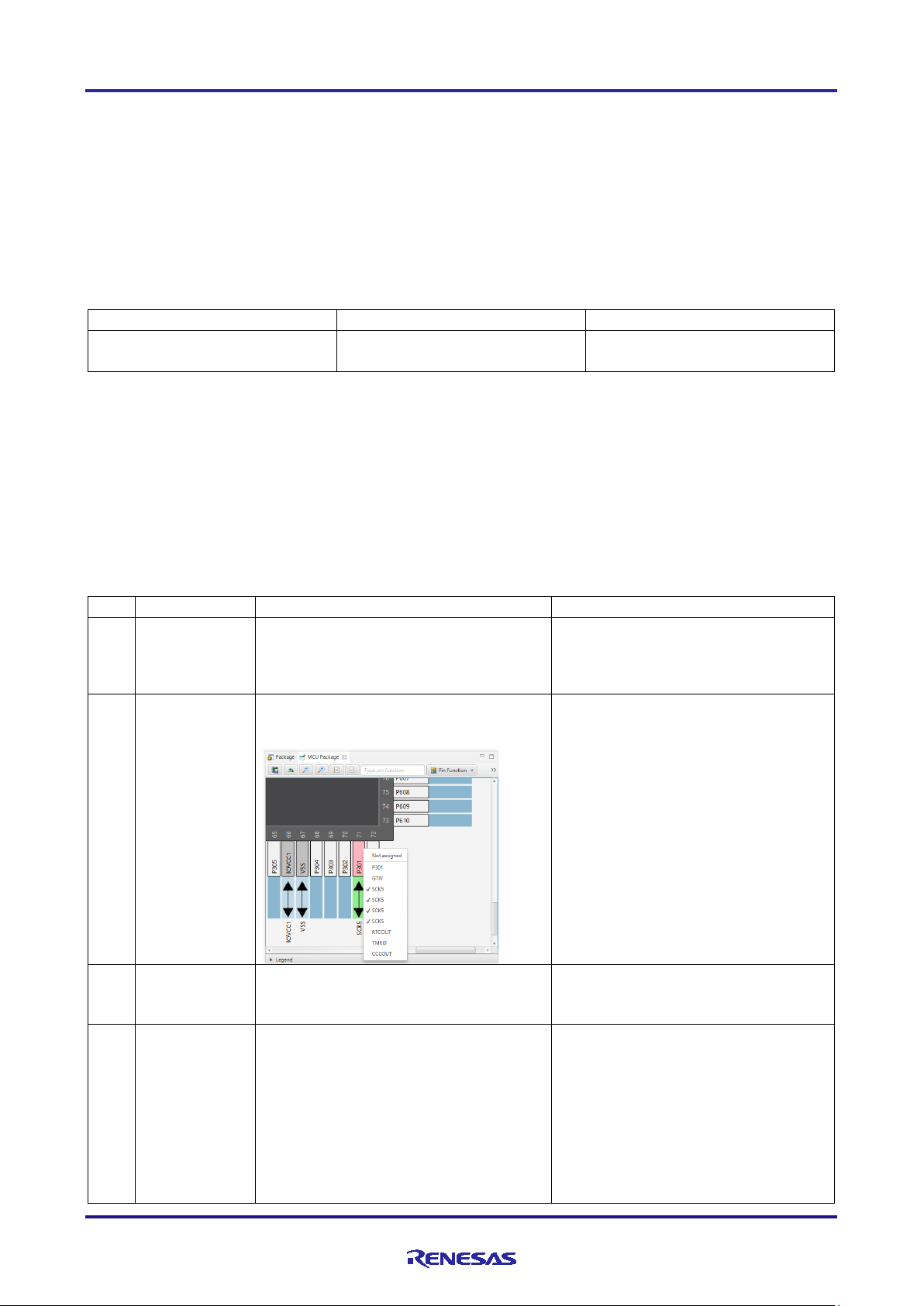
3
Pin settings
Group]
If SCK5 is selected, the terminal group
Even if you are using SCK5, customer
4
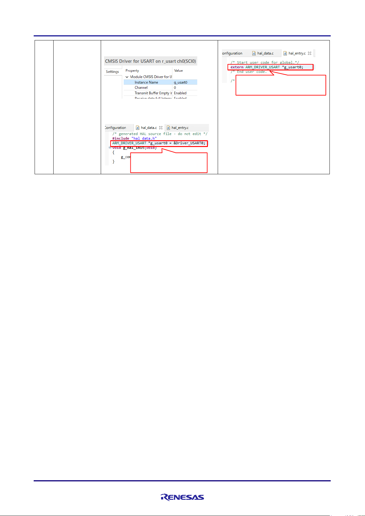
Driver
The instance created by the configurator
Describe the external reference
2. Operating Environment
2.1 Device
RE Family RE01 1500KB Group
RE Family RE01 256KB Group
2.2 Development Environment
It is recommended to use CMSIS package with the development environment listed below:
Table 2.1 Development Environment (Recommended)
later
Segger J-Link(OB)
3. Improvements from Older Version
There are no improvements. Because this is first release version.
4. Restrictions
4.1 Restriction List
For the latest complete list of restrictions, please see the tool news of this package on our website.
Table 4.1 Restriction List
option settings
evaluation criteria when starting a RE
FSP project.
MCU package screen, the terminal
name may be displayed in duplicate.
Settings in the introductory material
(R20UT4936) introduced in Chapter 1
overlapping terminals, so set one of
them.
[RE01 1500KB
R01AN5646EJ0100 Rev.1.00 Page 3 of 5
Jan.21.21
instance
is "SCK5_B" and "_ C" cannot be
selected.
cannot be used in the user program
because it has not been declared as an
external reference.
can use it regardless of the suffix
group.
declaration of the instance in the user
program.
RE01 1500KB Group, 256KB Group Flexible Software Package Rev1.00
Example: For USART driver
•
•
The instance has not been
declared an external reference.
Example: For USART driver
Describe the external reference
declaration of the instance in the user
program.
Configurator settings
Generated instance
(hal_data.c)
R01AN5646EJ0100 Rev.1.00 Page 4 of 5
Jan.21.21

RE01 1500KB Group, 256KB Group Flexible Software Package Rev1.00
Rev.
Date
Description
Page
Summary
1.00
Jan.21.21
First edition issued
Revision History
R01AN5646EJ0100 Rev.1.00 Page 5 of 5
Jan.21.21

General Precautions in the Handling of Microprocessing Unit and Microcontroller
Unit Products
The following usage notes are applicable to all Microprocessing unit and Microcontroller unit products from Renesas. For detailed usage notes on the
products covered by this document, refer to the relevant sections of the document as well as any technical updates that have been issued for the products.
1. Precaution against Electrostatic Discharge (ESD)
A strong electrical field, when exposed to a CMOS device, can cause destruction of the gate oxide and ultimately degrade the device operation. Steps
must be taken to stop the generation of static electricity as much as possible, and quickly dissipate it when it occurs. Environmental control must be
adequate. When it is dry, a humidifier should be used. This is recommended to avoid using insulators that can easily build up static electricity.
Semiconductor devices must be stored and transported in an anti-static container, static shielding bag or conductive material. All test and
measurement tools including work benches and floors must be grounded. The operator must also be grounded using a wrist strap. Semiconductor
devices must not be touched with bare hands. Similar precautions must be taken for printed circuit boards with mounted semiconductor devices.
2. Processing at power-on
The state of the product is undefined at the time when power is supplied. The states of internal circuits in the LSI are indeterminate and the states of
register settings and pins are undefined at the time when power is supplied. In a finished product where the reset signal is applied to the external reset
pin, the states of pins are not guaranteed from the time when power is supplied until the reset process is completed. In a similar way, the states of pins
in a product that is reset by an on-chip power-on reset function are not guaranteed from the time when power is supplied until the power reaches the
level at which resetting is specified.
3. Input of signal during power-off state
Do not input signals or an I/O pull-up power supply while the device is powered off. The current injection that results from input of such a signal or I/O
pull-up power supply may cause malfunction and the abnormal current that passes in the device at this time may cause degradation of internal
elements. Follow the guideline for input signal during power-off state as described in your product documentation.
4. Handling of unused pins
Handle unused pins in accordance with the directions given under handling of unused pins in the manual. The input pins of CMOS products are
generally in the high-impedance state. In operation with an unused pin in the open-circuit state, extra electromagnetic noise is induced in the vicinity of
the LSI, an associated shoot-through current flows internally, and malfunctions occur due to the false recognition of the pin state as an input signal
become possible.
5. Clock signals
After applying a reset, only release the reset line after the operating clock signal becomes stable. When switching the clock signal during program
execution, wait until the target clock signal is stabilized. When the clock signal is generated with an external resonator or from an external oscillator
during a reset, ensure that the reset line is only released after full stabilization of the clock signal. Additionally, when switching to a clock signal
produced with an external resonator or by an external oscillator while program execution is in progress, wait until the target clock signal is stable.
6. Voltage application waveform at input pin
Waveform distortion due to input noise or a reflected wave may cause malfunction. If the input of the CMOS device stays in the area between V
(Max.) and V
input level is fixed, and also in the transition period when the input level passes through the area between V
7. Prohibition of access to reserved addresses
Access to reserved addresses is prohibited. The reserved addresses are provided for possible future expansion of functions. Do not access these
addresses as the correct operation of the LSI is not guaranteed.
8. Differences between products
Before changing from one product to another, for example to a product with a different part number, confirm that the change will not lead to problems.
The characteristics of a microprocessing unit or microcontroller unit products in the same group but having a different part number might differ in terms
of internal memory capacity, layout pattern, and other factors, which can affect the ranges of electrical characteristics, such as characteristic values,
operating margins, immunity to noise, and amount of radiated noise. When changing to a product with a different part number, implement a system-
evaluation test for the given product.
(Min.) due to noise, for example, the device may malfunction. Take care to prevent chattering noise from entering the device when the
IH
(Max.) and VIH (Min.).
IL
IL

Corporate Headquarters
Contact information
www.renesas.com
Trademarks
of their respective owners.
Notice
1. Descriptions of circuits, software and other related information in this document are provided only to illustrate the operation of semiconductor products
and application examples. You are fully responsible for the incorporation or any other use of the circuits, software, and information in the design of your
product or system. Renesas Electronics disclaims any and all liability for any losses and damages incurred by you or third parties arising from the use
of these circuits, software, or information.
2. Renesas Electronics hereby expressly disclaims any warranties against and liability for infringement or any other claims involving patents, copyrights,
or other intellectual property rights of third parties, by or arising from the use of Renesas Electronics products or technical information described in this
document, including but not limited to, the product data, drawings, charts, programs, algorithms, and application examples.
3. No license, express, implied or otherwise, is granted hereby under any patents, copyrights or other intellectual property rights of Renesas Electronics
or others.
4. You shall be responsible for determining what licenses are required from any third parties, and obtaining such licenses for the lawful import, export,
manufacture, sales, utilization, distribution or other disposal of any products incorporating Renesas Electronics products, if required.
5. You shall not alter, modify, copy, or reverse engineer any Renesas Electronics product, whether in whole or in part. Renesas Electronics disclaims any
and all liability for any losses or damages incurred by you or third parties arising from such alteration, modification, copying or reverse engineering.
6. Renesas Electronics products are classified according to the following two quality grades: “Standard” and “High Quality”. The intended applications for
each Renesas Electronics product depends on the product’s quality grade, as indicated below.
"Standard": Computers; office equipment; communications equipment; test and measurement equipment; audio and visual equipment; home
"High Quality": Transportation equipment (automobiles, trains, ships, etc.); traffic control (traffic lights); large-scale communication equipment; key
Unless expressly designated as a high reliability product or a product for harsh environments in a Renesas Electronics data sheet or other Renesas
Electronics document, Renesas Electronics products are not intended or authorized for use in products or systems that may pose a direct threat to
human life or bodily injury (artificial life support devices or systems; surgical implantations; etc.), or may cause serious property damage (space
system; undersea repeaters; nuclear power control systems; aircraft control systems; key plant systems; military equipment; etc.). Renesas Electronics
disclaims any and all liability for any damages or losses incurred by you or any third parties arising from the use of any Renesas Electronics product
that is inconsistent with any Renesas Electronics data sheet, user’s manual or other Renesas Electronics document.
7. No semiconductor product is absolutely secure. Notwithstanding any security measures or features that may be implemented in Renesas Electronics
hardware or software products, Renesas Electronics shall have absolutely no liability arising out of any vulnerability or security breach, including but
not limited to any unauthorized access to or use of a Renesas Electronics product or a system that uses a Renesas Electronics product. RENESAS
ELECTRONICS DOES NOT WARRANT OR GUARANTEE THAT RENESAS ELECTRONICS PRODUCTS, OR ANY SYSTEMS CREATED USING
RENESAS ELECTRONICS PRODUCTS WILL BE INVULNERABLE OR FREE FROM CORRUPTION, ATTACK, VIRUSES, INTERFERENCE,
HACKING, DATA LOSS OR THEFT, OR OTHER SECURITY INTRUSION (“Vulnerability Issues”). RENESAS ELECTRONICS DISCLAIMS ANY AND
ALL RESPONSIBILITY OR LIABILITY ARISING FROM OR RELATED TO ANY VULNERABILITY ISSUES. FURTHERMORE, TO THE EXTENT
PERMITTED BY APPLICABLE LAW, RENESAS ELECTRONICS DISCLAIMS ANY AND ALL WARRANTIES, EXPRESS OR IMPLIED, WITH
RESPECT TO THIS DOCUMENT AND ANY RELATED OR ACCOMPANYING SOFTWARE OR HARDWARE, INCLUDING BUT NOT LIMITED TO
THE IMPLIED WARRANTIES OF MERCHANTABILITY, OR FITNESS FOR A PARTICULAR PURPOSE.
8. When using Renesas Electronics products, refer to the latest product information (data sheets, user’s manuals, application notes, “General Notes for
Handling and Using Semiconductor Devices” in the reliability handbook, etc.), and ensure that usage conditions are within the ranges specified by
Renesas Electronics with respect to maximum ratings, operating power supply voltage range, heat dissipation characteristics, installation, etc. Renesas
Electronics disclaims any and all liability for any malfunctions, failure or accident arising out of the use of Renesas Electronics products outside of such
specified ranges.
9. Although Renesas Electronics endeavors to improve the quality and reliability of Renesas Electronics products, semiconductor products have specific
characteristics, such as the occurrence of failure at a certain rate and malfunctions under certain use conditions. Unless designated as a high reliability
product or a product for harsh environments in a Renesas Electronics data sheet or other Renesas Electronics document, Renesas Electronics
products are not subject to radiation resistance design. You are responsible for implementing safety measures to guard against the possibility of bodily
injury, injury or damage caused by fire, and/or danger to the public in the event of a failure or malfunction of Renesas Electronics products, such as
safety design for hardware and software, including but not limited to redundancy, fire control and malfunction prevention, appropriate treatment for
aging degradation or any other appropriate measures. Because the evaluation of microcomputer software alone is very difficult and impractical, you are
responsible for evaluating the safety of the final products or systems manufactured by you.
10. Please contact a Renesas Electronics sales office for details as to environmental matters such as the environmental compatibility of each Renesas
Electronics product. You are responsible for carefully and sufficiently investigating applicable laws and regulations that regulate the inclusion or use of
controlled substances, including without limitation, the EU RoHS Directive, and using Renesas Electronics products in compliance with all these
applicable laws and regulations. Renesas Electronics disclaims any and all liability for damages or losses occurring as a result of your noncompliance
with applicable laws and regulations.
11. Renesas Electronics products and technologies shall not be used for or incorporated into any products or systems whose manufacture, use, or sale is
prohibited under any applicable domestic or foreign laws or regulations. You shall comply with any applicable export control laws and regulations
promulgated and administered by the governments of any countries asserting jurisdiction over the parties or transactions.
12. It is the responsibility of the buyer or distributor of Renesas Electronics products, or any other party who distributes, disposes of, or otherwise sells or
transfers the product to a third party, to notify such third party in advance of the contents and conditions set forth in this document.
13. This document shall not be reprinted, reproduced or duplicated in any form, in whole or in part, without prior written consent of Renesas Electronics.
14. Please contact a Renesas Electronics sales office if you have any questions regarding the information contained in this document or Renesas
Electronics products.
(Note1) “Renesas Electronics” as used in this document means Renesas Electronics Corporation and also includes its directly or indirectly controlled
(Note2) “Renesas Electronics product(s)” means any product developed or manufactured by or for Renesas Electronics.
subsidiaries.
electronic appliances; machine tools; personal electronic equipment; industrial robots; etc.
financial terminal systems; safety control equipment; etc.
(Rev.5.0-1 October 2020)
TOYOSU FORESIA, 3-2-24 Toyosu,
Koto-ku, Tokyo 135-0061, Japan
Renesas and the Renesas logo are trademarks of Renesas Electronics
Corporation. All trademarks and registered trademarks are the property
For further information on a product, technology, the most up-to-date
version of a document, or your nearest sales office, please visit:
www.renesas.com/contact/
.
© 2021 Renesas Electronics Corporation. All rights reserved.
 Loading...