

Page 1

16
Rev.1.02 2021.4
R
32
RE01 Group
)
ual
User's Manual
Evaluation Kit RE01 256KB (EK-RE01 256KB
User’s Man
E Family/RE0 Series
All information contained in these materials, including products and product specifications,
represents information on the product at the time of publication and is subject to change by
Renesas Electronics Corporation without notice. Please review the latest information published by
Renesas Electronics Corporation through various means, including the Renesas Electronics
Corporation website (http://www.renesas.com).
Page 2

Notice
Corporate Headquarters
Contact information
Trademarks
1. Descriptions of circuits, software and other related information in this document are provided only to illustrate the operation of semiconductor products
and application examples. You are fully responsible for the incorporation or any other use of the circuits, software, and information in the design of your
product or system. Renesas Electronics disclaims any and all liability for any losses and damages incurred by you or third parties arising from the use of
these circuits, software, or information.
2. Renesas Electronics hereby expressly disclaims any warranties against and liability for infringement or any other claims involving patents, copyrights, or
other intellectual property rights of third parties, by or arising from the use of Renesas Electronics products or technical information described in this
document, including but not limited to, the product data, drawings, charts, programs, algorithms, and application examples.
3. No license, express, implied or otherwise, is granted hereby under any patents, copyrights or other intellectual property rights of Renesas Electronics or
others.
4. You shall be responsible for determining what licenses are required from any third parties, and obtaining such licenses for the lawful import, export,
manufacture, sales, utilization, distribution or other disposal of any products incorporating Renesas Electronics products, if required.
5. You shall not alter, modify, copy, or reverse engineer any Renesas Electronics product, whether in whole or in part. Renesas Electronics disclaims any
and all liability for any losses or dam ages incurred by you or third parties arising from such alteration, modification, copying or reverse engineering.
6. Renesas Electronics products are classified according to the following two quality grades: “Standard” and “High Quality”. The intended applications for
each Renesas Electronics product depends on the product’s quality grade, as indicated below.
"Standard": Computers; office equipment; communications equipment; test and measurement equipment; audio and visual equipment; home
"High Quality": Transportation equipment (automobiles, trains, ships, etc.); traffic control (traffic lights); large-scale communication equipment; key
Unless expressly designated as a high reliability product or a product for harsh environments in a Renesas Electronics data sheet or other Renesas
Electronics document, Renesas Electronics products are not intended or authorized for use in products or systems that may pose a direct threat to
human life or bodily injury (artificial life support devices or systems; surgical implantations; etc.), or may cause serious property damage (space system;
undersea repeaters; nuclear power control systems; aircraft control systems; key plant systems; military equipment; etc.). Renesas Electronics disclaims
any and all liability for any damages or losses incurred by you or any third parties arising from the use of any Renesas Electronics product that is
inconsistent with any Renesas Electronics data sheet, user’s manual or other Renesas Electronics document.
7. No semiconductor product is absolutely secure. Notwithstanding any security measures or features that may be implemented in Renesas Electronics
hardware or software products, Renesas Electronics shall have absolutely no liability arising out of any vulnerability or security breach, including but not
limited to any unauthorized access to or use of a Renesas Electronics product or a system that uses a Renesas Electronics product. RENESAS
ELECTRONICS DOES NOT WARRANT OR GUARANTEE THAT RENESAS ELECTRONICS PRODUCTS, OR ANY SYSTEMS CREATED USING
RENESAS ELECTRONICS PRODUCTS WILL BE INVULNERABLE OR FREE FROM CORRUPTION, ATTACK, VIRUSES, INTERFERENCE,
HACKING, DATA LOSS OR THEFT, OR OTHER SECURITY INTRUSION (“Vulnerability Issues”). RENESAS ELECTRONICS DISCLAIMS ANY AND
ALL RESPONSIBILITY OR LIABILITY ARISING FROM OR RELATED TO ANY VULNERABILITY ISSUES. FURTHERMORE, TO THE EXTENT
PERMITTED BY APPLICABLE LAW, RENESAS ELECTRONICS DISCLAIMS ANY AND ALL WARRANTIES, EXPRESS OR IMPLIED, WITH
RESPECT TO THIS DOCUMENT AND ANY RELATED OR ACCOMPANYING SOFTWARE OR HARDWARE, INCLUDING BUT NOT LIMITED TO THE
IMPLIED WARRANTIES OF MERCHANTABILITY, OR FITNESS FOR A PARTICULAR PURPOSE.
8. When using Renesas Electronics products, refer to the latest product information (data sheets, user’s manuals, application notes, “General Notes for
Handling and Using Semiconductor Devices” in the reliability handbook, etc.), and ensure that usage conditions are within the ranges specified by
Renesas Electronics with respect to maximum ratings, operating power supply voltage range, heat dissipation characteristics, installation, etc. Renesas
Electronics disclaims any and all liability for any malfunctions, failure or accident arising out of the use of Renesas Electronics products outside of such
specified ranges.
9. Although Renesas Electronics endeavors to improve the quality and reliability of Renesas Electronics products, semiconductor products have specific
characteristics, such as the occurrence of failure at a certain rate and malfunctions under certain use conditions. Unless designated as a high reliability
product or a product for harsh environments in a Renesas Electronics data sheet or other Renesas Electronics document, Renesas Electronics products
are not subject to radiation resistance design. You are responsible for implementing safety measures to guard against the possibility of bodily injury,
injury or damage caused by fire, and/or danger to the public in the event of a failure or malfunction of Renesas Electronics products, such as safety
design for hardware and software, including but not limited to redundancy, fire control and malfunction prevention, appropriate treatment for aging
degradation or any other appropriate measures. Because the evaluation of microcomputer software alone is very difficult and impractical, you are
responsible for evaluating the safety of the final products or systems manufactured by you.
10. Please contact a Renesas Electronics sales office for details as to environmental matters such as the environmental compatibility of each Renesas
Electronics product. You are responsible for carefully and sufficiently investigating applicable laws and regulations that regulate the inclusion or use of
controlled substances, including without limitation, the EU RoHS Directive, and using Renesas Electronics products in compliance with all these
applicable laws and regulations. Renesas Electronics disclaims any and all liability for damages or losses occurring as a result of your noncompliance
with applicable law s and regulations.
11. Renesas Electronics products and technologies shall not be used for or incorporated into any products or systems whose manufacture, use, or sale is
prohibited under any applicable domestic or foreign laws or regulations. You shall comply with any applicable export control laws and regulations
promulgated and administered by the governments of any countries asserting jurisdiction over the parties or transactions.
12. It is the responsibility of the buyer or distributor of Renesas Electronics products, or any other party who distributes, disposes of, or otherwise sells or
transfers the product to a third party, to notify such third party in advance of the contents and conditions set forth in this document.
13. This document shall not be reprinted, reproduced or duplicated in any form, i n whole or in part, without prior written consent of Renesas Electronics.
14. Please contact a Renesas Electronics sales office if you have any questions regarding the information contained in this document or Renesas
Electronics products.
(Note1) “Renesas Electronics” as used in this document means Renesas Electronics Corporation and also includes its directly or indirectly controlled subsidiaries.
(Note2) “Renesas Electronics product(s)” means any product developed or manufactured by or for Renesas Electronics.
electronic appliances; machine tools; personal electronic equipment; industrial robots; etc.
financial terminal systems; safety control equipment; etc.
(Rev.5.0-1 October 2020)
TOYOSU FORESIA, 3-2-24 Toyosu,
Koto-ku, Tokyo 135-0061, Japan
www.renesas.com
Renesas and the Renesas logo are trademarks of Renesas
Electronics Corporation. All trademarks and registered trademarks
are the property of their respective owners.
For further information on a product, technology, the most up-to-date
version of a document, or your nearest sales office, please visit:
www.renesas.com/contact/.
Page 3

General Precautions in the Handling of Microprocessing Unit and Microcontroller
Unit Products
The following usage notes are applicable to all Microprocessing unit and Microcontroller unit products from Renesas. For detailed usage notes on the
products covered by this document, refer to the relevant sections of the document as well as any technical updates that have been issued for the products.
1. Precaution against Electrostatic Discharge (ESD)
A strong electrical field, when exposed to a CMOS device, can cause destruction of the gate oxide and ultimately degrade the device operation. Steps
must be taken to stop the generation of static electricity as much as possible, and quickly dissipate it when it occurs. Environmental control must be
adequate. When it is dry, a humidifier should be used. This is recommended to avoid using insulators that can easily build up static electricity.
Semiconductor devi ces must be stored and transported in an anti-static container, static shielding bag or conductive material. All test and measurement
tools including work benches and floors must be grounded. The operator must also be grounded using a wrist strap. Semiconductor devices must not be
touched with bare hands. Similar precautions must be taken for printed circuit boards with mounted semiconductor devices.
2. Processing at power-on
The state of the product is undefined at the time when power is supplied. The states of internal circuits in the LSI are indeterminate and the states of
register settings and pins are undefined at the time when power is supplied. In a finished product where the reset signal is applied to the external reset
pin, the states of pins are not guaranteed from the time when power is supplied until the reset process is completed. In a similar way, the states of pins in
a product that is reset by an on-chip power-on reset function are not guaranteed from the time when power is supplied until the power reaches the level
at which resetting is specified.
3. Input of signal during power-off state
Do not input signals or an I/O pull-up power supply while the device is powered off. The current injection that results from input of such a signal or I/O
pull-up power supply may cause malfunction and the abnormal current that passes in the device at this time may cause degradation of internal elements.
Follow the guideline for input signal during power-off state as described in your product documentation.
4. Handling of unused pins
Handle unused pins in accordance with the directions given under handling of unused pins in the manual. The input pins of CMOS products are
generally in the high-impedance state. In operation with an unused pin in the open-circuit state, extra electromagnetic noise is induced in the vicinity of
the LSI, an associated shoot-through current flows internally, and malfunctions occur due to the false recognition of the pin state as an input signal
become possible.
5. Clock signals
After applying a reset, only release the reset line after the operating clock signal becomes stable. When switchi ng the clock signal during program
execution, wait until the target clock signal is stabilized. When the clock signal is generated with an external resonator or from an external oscillator
during a reset, ensure that the reset line is only released after full stabilization of the clock signal. Additionally, when switching to a clock signal produced
with an external resonator or by an external oscillator while program execution is in progress, wait until the target clock signal is stable.
6. Voltage application waveform at input pin
Waveform distortion due to input noise or a reflected wave may cause malfunction. If the input of the CMOS device stays in the area between V
and V
(Min.) due to noise, for example, the device may malfunction. Take care to prevent chattering noise from entering the device when the input level
IH
is fixed, and also in the transition period when the input level passes through the area between V
7. Prohibition of access to reserved addresses
Access to reserved addresses is prohibited. The reserved addresses are provided for possible future expansion of functions. Do not access these
addresses as the correct operation of the LSI is not guaranteed.
8. Differences between products
Before changing from one product to another, for example to a product with a different part number, confirm that the change will not lead to problems.
The characteristics of a microprocessing unit or microcontroller unit products in the same group but having a different part number might differ in terms of
internal memory capacity, layout pattern, and other factors, which can affect the ranges of electrical characteristics, such as characteristic values,
operating margins, immunity to noise, and amount of radiated noise. When changing to a product with a different part number, implement a system-
evaluation test for the given product.
(Max.) and VIH (Min.).
IL
(Max.)
IL
Page 4

Disclaimer
The Evaluation Kit is not guaranteed to be error free, and the entire risk as to the results and performance of the
By using this Evaluation Kit, the user accepts the following terms:
Evaluation Kit is assumed by the User. The Evaluation Kit is provided by Renesas on an “as is” basis without
warranty of any kind whether express or implied, including but not limited to the implied warranties of satisfactory
quality, fitness for a particular purpose, title and non-infringement of intellectual property rights with regard to the
Evaluation Kit. Renesas expressly disclaims all such warranties. Renesas or its affiliates shall in no event be liable
for any loss of profit, loss of data, loss of contract, loss of business, damage to reputation or goodwill, any economic
loss, any reprogramming or recall costs (whether the foregoing losses are direct or indirect) nor shall Renesas or its
affiliates be liable for any other direct or indirect special, incidental or consequential damages arising out of or in
relation to the use of this Evaluation Kit, even if Renesas or its affiliates have been advised of the possibility of such
damages.
Precautions
The following precautions should be observed when operating any Evaluation Kit product:
This Evaluation Kit is only intended for use in a laboratory environment under ambient temperature and humidity
conditions. A safe separation distance should be used between this and any sensitive equipment. Its use outside the
laboratory, classroom, study area or similar such area invalidates conformity with the protection requirements of the
Electromagnetic Compatibility Directive and could lead to prosecution.
The product generates, uses, and can radiate radio frequency energy and may cause harmful interference to radio
communications. However, there is no guarantee that interference will not occur in a particular installation. If this
equipment causes harmful interference to radio or television reception, which can be determined by turning the
equipment off or on, you are encouraged to try to correct the interference by one or more of the following measures;
• ensure attached cables do not lie across the equipment
• reorient the receiving antenna
• increase the distance between the equipment and the receiver
• connect the equipment into an outlet on a circuit different from that which the receiver is connected
• power down the equipment when not in use
• consult the dealer or an experienced radio/TV technician for help NOTE: It is recommended that wherever
possible shielded interface cables are used.
The product is potentially susceptible to certain EMC phenomena. To mitigate against them it is recommended that
the following measures be undertaken;
• The user is advised that mobile phones should not be used within 10m of the product when in use.
• The user is advised to take ESD precautions when handling the equipment.
The Evaluation Kit does not represent an ideal reference design for an end product and does not fulfil the regulatory
standards for an end product.
Page 5
How to Use This Manual
Document Type
Description
Document Title
Document No.
f the
Evaluation Kit hardware.
User’s Manual
(This manual)
p
and run the first sample.
schematics of the
Evaluation Kit Main Board.
main board schematics
il circuit schematics of the
MIP-LCD Expansion Board.
schematics
User’s Manual: Hardware RE01
1.Objective and Target Users
This manual is designed to provide the user with an understanding of the Evaluation Kit Evaluation Board
hardware functionality, and electrical characteristics. It is intended for users designing sample code on the
Evaluation Kit Evaluation Board platform, using the many different incorporated peripheral devices.
The manual comprises of an overview of the capabilities of the Evaluation Kit product, but does not intend to
be a guide to embedded programming or hardware design.
Particular attention should be paid to the precautionary notes when using the manual. These notes occur within the body
of the text, at the end of each section, and in the Usage Notes section.
The revision history summarizes the locations of revisions and additions. It does not list all revisions. Refer to the text of
the manual for details.
The following documents apply to Evaluation Kit for RE01 256KB. Make sure to refer to the latest versions of
these documents. The newest versions of the documents listed may be obtained from the Renesas
Electronics Web site.
User’s Manual Describes the technical details o
Quick Start Guide Provides simple instructions setu
the Evaluation Kit for RE01 256KB
Schematics Full detail circuit
Schematics Full deta
Hardware Manual Provides technical details of the
RE01 device.
Evaluation Kit RE01 256KB
Evaluation Kit RE01 256KB
Quick Start Guide
Evaluation Kit RE01 256KB
MIP-LCD expansion board
RE01 Group Products with
256-Kbyte Flash Memory
R20UT4801EJ
R20UT4808EJ
R20UT4802EJ
R20UT4564EJ
R01UH0894JJ
Page 6

List of Abbreviations and Acronyms
Abbreviation
Full Form
BLE
Bluetooth Low Energy
DNF
Do Not Fit
E2
Renesas On-chip Debugging Emulator
EH
Energy Harvesting
EHC
Energy Harvesting Control Circuit
EMC
Electromagnetic Compatibility
ESD
Electrostatic Discharge
IRQ
Interrupt Request
LDO
Low Dropout
LED
Light Emitting Diode
MIP-LCD
Memory In Pixel - Liquid Crystal Display
MLCD
Memory In Pixel - Liquid Crystal Display
PC
Personal Computer
RAM
Random Access Memory
RFP
Renesas Flash Programmer
SCI
Serial Communications Interface
SPI
Serial Peripheral Interface
USB
Universal Serial Bus
All trademarks and registered trademarks are the property of their respective owners.
2.
FPC Flexible Printed Circuits
I-jetTM IAR System® JTAG Emulator
J-LinkTM SEGGER debug probe
J-LinkTM OB SEGGER On-board debug probe
n/c (NC) Not Connected
Pmod™
This is a Digilent Pmod™ Compatible connector. Pmod™ is registered to Digilent Inc.
Digilent-Pmod_Interface_Specification
Page 7

Table of Contents
1. Overview ........................................................................................................................................................... 9
1.1 Purpose ...................................................................................................................................................... 9
1.2 Kit Contents ............................................................................................................................................... 9
1.3 Board Specifications ................................................................................................................................ 10
1.4 Board Exterior .......................................................................................................................................... 12
2. Board Layout .................................................................................................................................................. 14
2.1 Component Layout ................................................................................................................................... 14
2.2 Board Dimensions .................................................................................................................................... 15
2.3 Component Placement ............................................................................................................................ 17
2.4 Board Initial Settings ................................................................................................................................ 20
3. Internal Board Connections ............................................................................................................................ 21
4. Power Supply .................................................................................................................................................. 24
4.1 Power Supply System .............................................................................................................................. 24
4.2 Power Supply Source .............................................................................................................................. 25
4.3 External Power Supply ............................................................................................................................. 26
5. Operation/Start-up Mode ................................................................................................................................ 32
5.1 Normal Operation ..................................................................................................................................... 32
5.2 EHC Operation ......................................................................................................................................... 33
5.3 RE01 Start-up Mode ................................................................................................................................ 42
6. Debug ............................................................................................................................................................. 43
6.1 J-LinkTM OB .............................................................................................................................................. 43
6.2 I-jetTM, J-LinkTM ......................................................................................................................................... 46
6.3 E2 ............................................................................................................................................................. 49
6.4 Flash Programmer -Renesas Flash Programmer- .................................................................................. 52
6.5 Flash Programmer -SEGGER J-Flash Lite- ............................................................................................. 57
6.6 Emulator connection in EHC mode .......................................................................................................... 58
7. Current Measurement Circuit ......................................................................................................................... 60
7.1 Current measurement when using the on-board regulator 3.3V ............................................................. 60
7.2 Current measurement when not using on-board regulator 3.3V ............................................................. 62
7.3 Current measurement during EHC operation .......................................................................................... 63
8. User Circuitry .................................................................................................................................................. 66
8.1 Reset Circuit ............................................................................................................................................ 66
8.2 Clock Circuit ............................................................................................................................................. 67
8.3 Switches ................................................................................................................................................... 68
8.4 LED .......................................................................................................................................................... 69
8.5 Pmod™ Interface ..................................................................................................................................... 70
8.6 USB Serial Conversion ............................................................................................................................ 75
8.7 MLCD (Memory In Pixel Liquid Crystal Display) Interface ....................................................................... 77
8.8 Flash Memory .......................................................................................................................................... 78
8.9 Arduino UNO Interface ............................................................................................................................. 79
8.10 External DC/DC Circuit ............................................................................................................................ 82
9. Headers .......................................................................................................................................................... 84
9.1 RE01 Headers ......................................................................................................................................... 84
10. Code Development ....................................................................................................................................... 88
10.1 Overview .................................................................................................................................................. 88
10.2 Mode Support .......................................................................................................................................... 88
10.3 Address Space ......................................................................................................................................... 88
Page 8

11. Additional Information ................................................................................................................................... 89
Page 9
No
Kit Contents
1
Main board
Part No.: RTK70E0118C00001BJ
2
MIP-LCD Expansion board
Part No.: RTK70E015DB00000BJ
3
Solar panel
Part No.: AM-1815CA (Panasonic)
4
USB cable
Type-A male to micro-B male
5
IC clip
Red, Black
Evaluation Kit RE01 256KB R20UT4801EJ0102
Rev.1.02
Apr 16, 2021
1. Overview
1.1 Purpose
This Evaluation Kit is an evaluation tool for Renesas RE01 device. This manual describes the technical
details of the Evaluation Kit hardware.
1.2 Kit Contents
Kit contents included in the Evaluation Kit are shown in Table 1-1.
Table 1-1: Kit Contents
R20UT4801EJ0102 Rev.1.02 Page 9 of 95
Apr 16, 2021
Page 10
Evaluation Kit RE01 256KB 1.Overview
Item
Specifications
Part No.: R7F0E01182CFP
Package: 100-pin LFQFP
On-chip memory: ROM 256KB, RAM 128KB
On-Board Memory
SPI Serial Flash: 64Mbit
RE01 Main: 32MHz
RE01 Sub: 32.768kHz
Debugger: 5V Input
Power Supply IC: 5V Input, 3.3V Output
Power Supply IC: 2.6V Input, 3.3V Output (For peripheral circuit power supply when
using energy harvesting function)
Power Supply IC: 2.6V or 3.3V Input, 1.25V Output (external DC/DC)
Power Supply IC: 2.6V or 3.3V Input, 0.85V Output (external DC/DC)
I-jetTM / J-Link
TM
/ E2 20-pin box header
USB Connector for J-LinkTM OB
Operation Mode Configuration: double-pole, double-throw x 4
Start-up Mode Configuration: single-pole, double-throw x 2
Internal LDO Configuration: double-pole, single-throw x 2
Reset Switch x 1
User Switch x 2
Discharge Switch x 2
Power Indicator: (Green) x 1
For users: (Orange) x 1, (Red) x 1
J-LinkTM OB Power Indicator: (Green) x 1
FPC Connector: 0.3mm pitch,19 pin x 1
MIP-LCD*5: TN0104ANVAANN-GN00(KYOCERA)
Connector: USB-MicroB
Driver: USB Interface IC (Part No. FT230XQ)
MIP-LCD Expansion Board
Interface
Pmod™
PMOD1 *2: Angle type、12-pin connector
External Battery Interface
3.5mm pitch: 2 pin x 1*3
Solar Panel Interface
2.54mm pitch: 2 pin x 1
Arduino UNO Interface
2.54mm pitch: 10 pin x 1 (J6),8 pin x 2 (J10, J18),6 pin x 1 (J19)
RE01 Header*4
2.54mm pitch: 50 pin x 2 (J7, J8, J9, J21)
1.3 Board Specifications
Board specifications are shown in Table 1-2
Table 1-2: Board Specifications
Target Device
Input Clock
Power Supply
、Table 1-3.
Debug Interface*
Slide Switch
Push Switch
1
LED
MLCD
USB Serial Converter Interface
*2
*1
: Use each debugger exclusively. When using J-Link OB, do not connect to other emulators. When using
2.54mm pitch: 12 pin x 1(PMOD1)
another emulator, do not connect to J-Link OB.
*2
: PMOD1 is used both for MIP-LCD Expansion Board and PmodTM.
*3
: The external battery is not included in this product.
*4
: The connector is not included in this product.
*5
: The MIP-LCD is not included in this product.
R20UT4801EJ0102 Rev.1.02 Page 10 of 95
Apr 16, 2021
Page 11

Evaluation Kit RE01 256KB 1.Overview
Item
Specification
Part No.: TN0181ANVNANN-AN00*1 (KYOCERA)
Size: 1.81 inch
Resolution: 200dpi (256(H) x 256(V))
Main Board Interface
2.54mm pitch: 12 pin x 1(PMOD1)
Table 1-3: MIP-LCD Expansion Board Specification
MIP-LCD
*1
: Please contact KYOCERA.
R20UT4801EJ0102 Rev.1.02 Page 11 of 95
Apr 16, 2021
Page 12
Evaluation Kit RE01 256KB 1.Overview
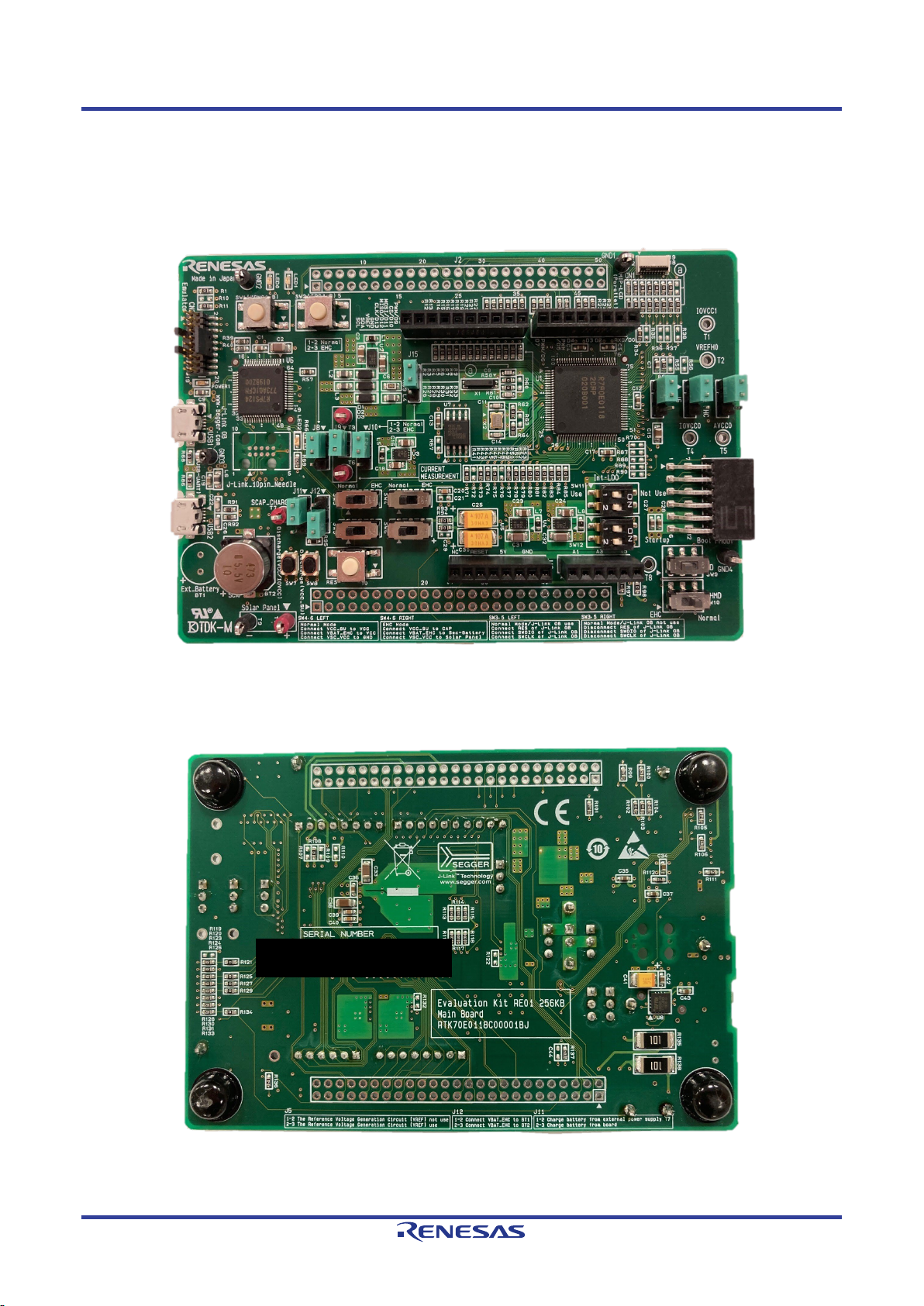
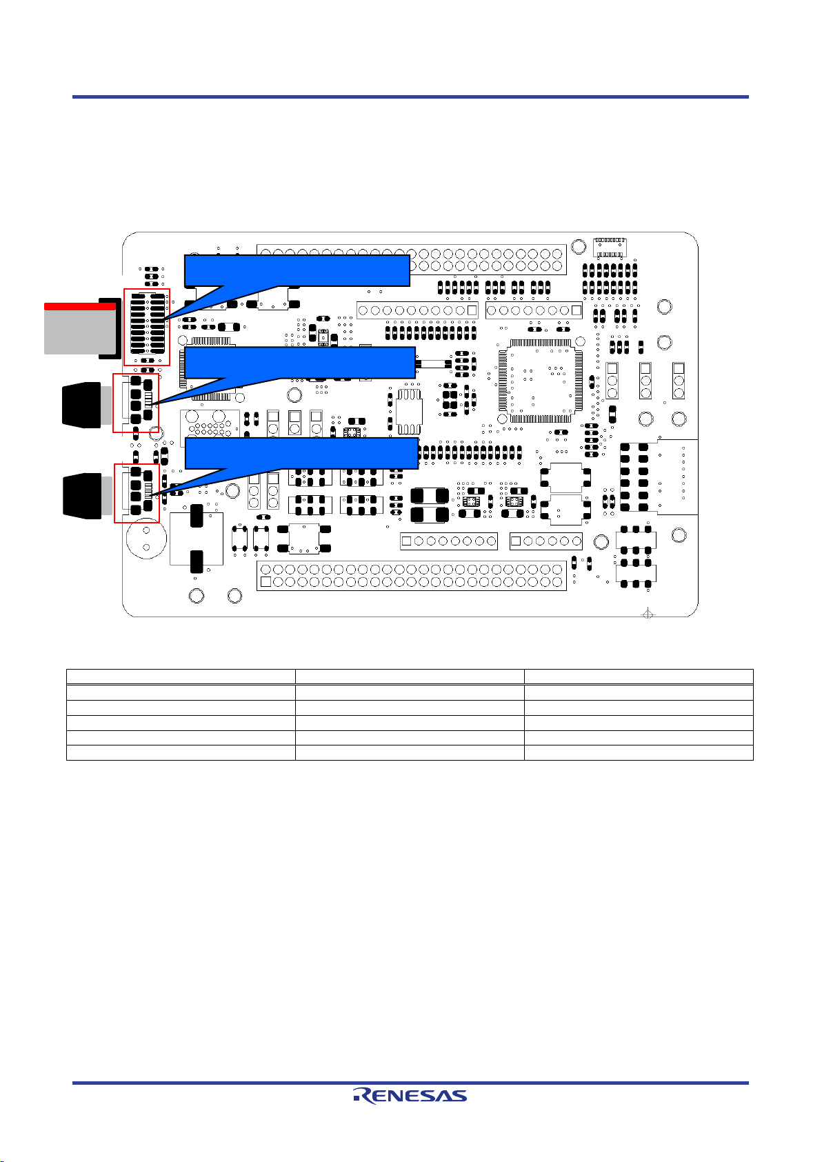
1.4 Board Exterior
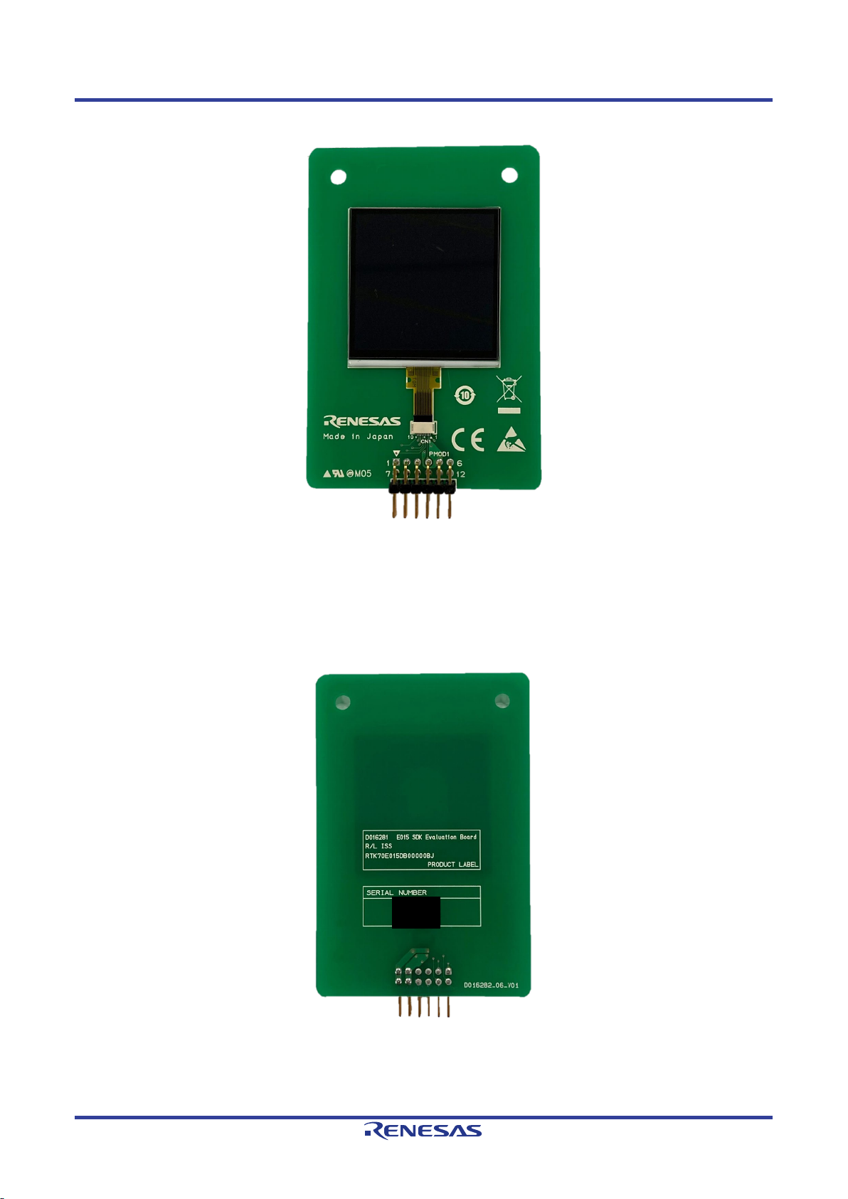
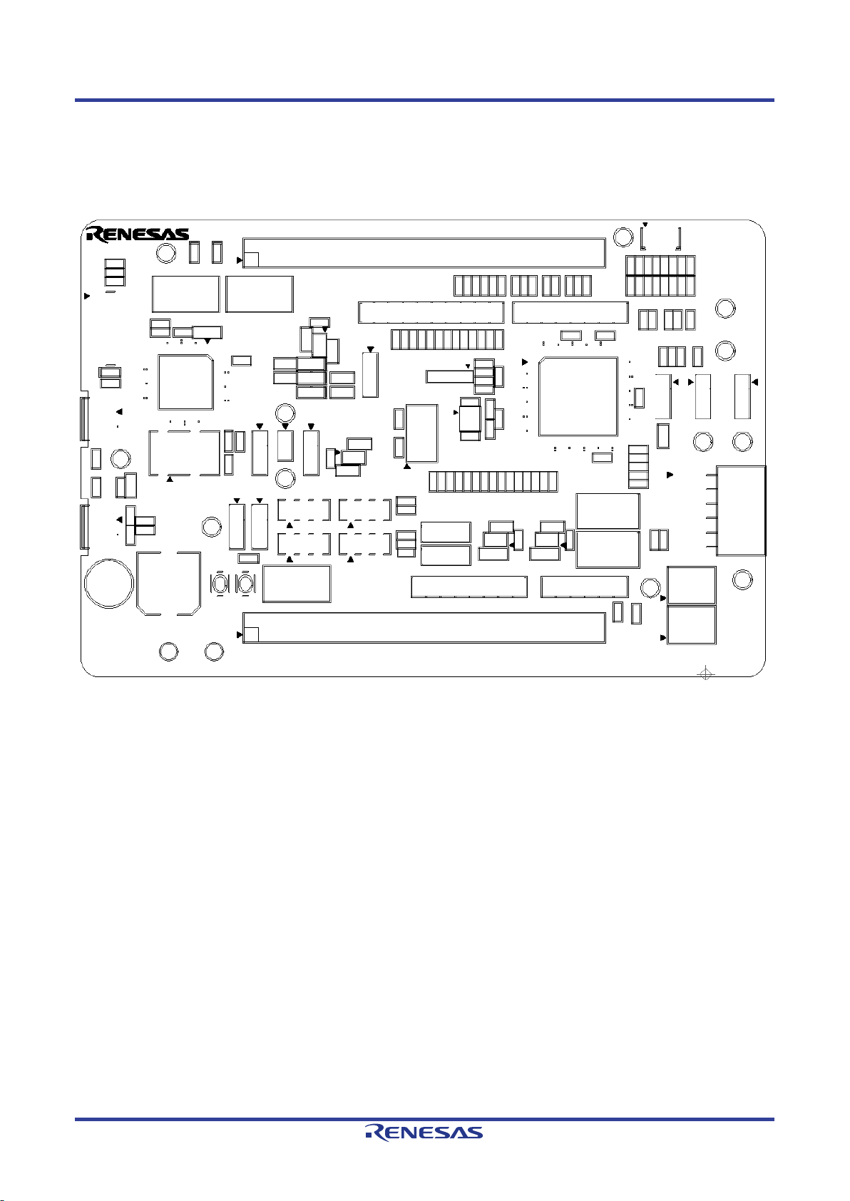
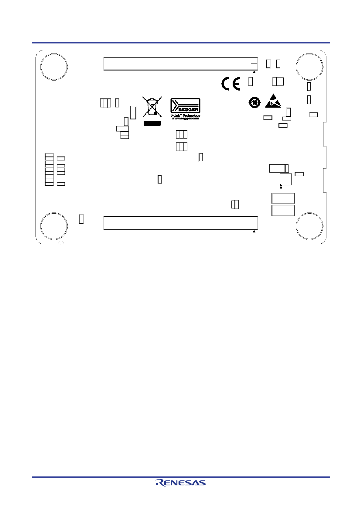
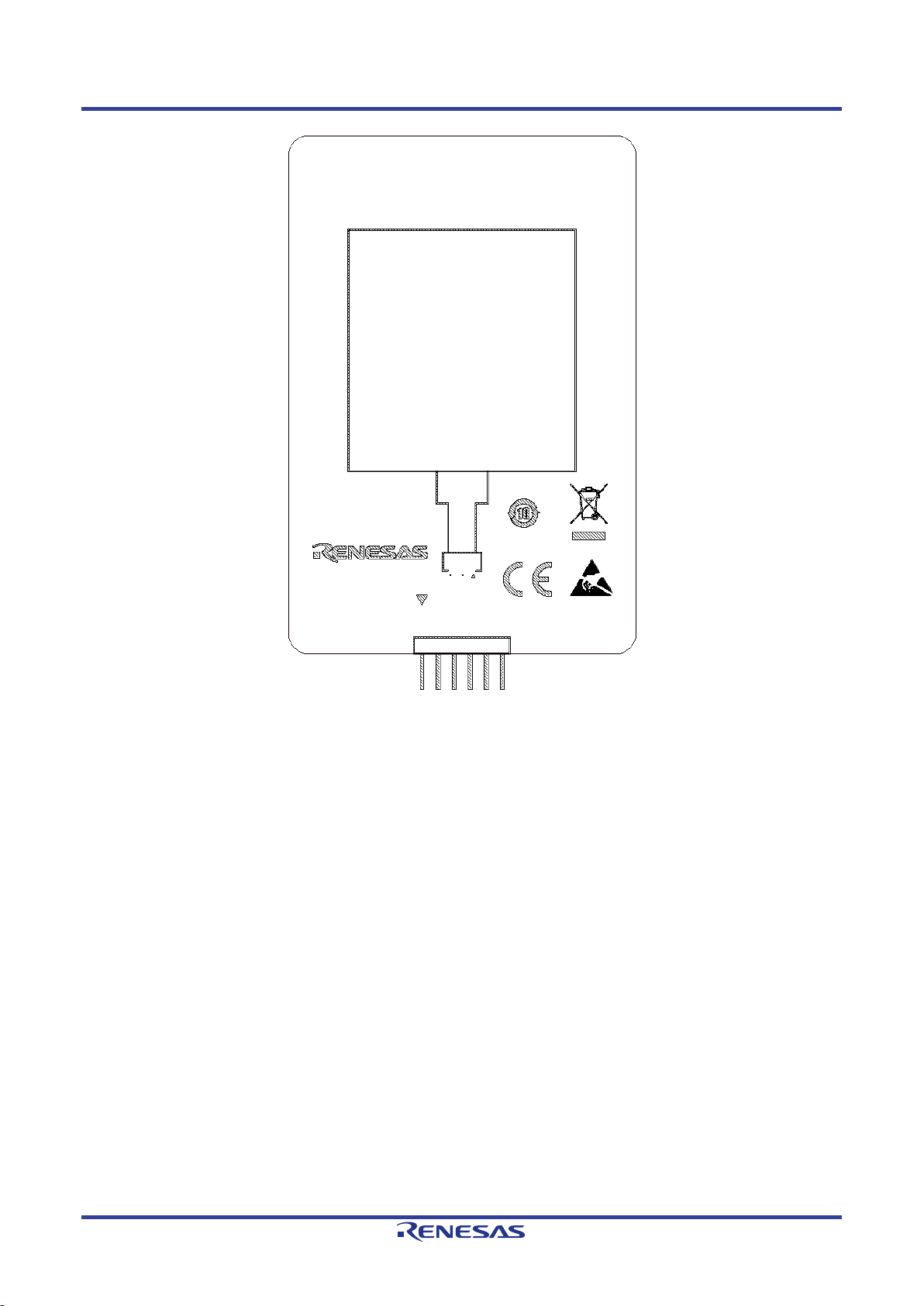
The exterior of Evaluation Kit RE01 256KB is shown in this chapter. Figure 1-1 and Figure 1-2 show the
exterior of the main board. Figure 1-3 and Figure 1-4 show the exterior of MIP-LCD expansion board.
Figure 1-1: Main Board (Top)
Figure 1-2: Main Board (Bottom)
R20UT4801EJ0102 Rev.1.02 Page 12 of 95
Apr 16, 2021
Page 13
Evaluation Kit RE01 256KB 1.Overview
Figure 1-3: MIP-LCD Expansion Board (Top)
Figure 1-4: MIP-LCD Expansion Board (Bottom)
R20UT4801EJ0102 Rev.1.02 Page 13 of 95
Apr 16, 2021
Page 14
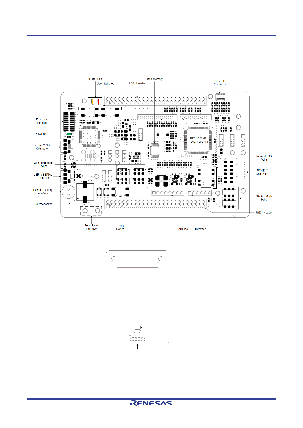
Evaluation Kit RE01 256KB 2.Board Layout
MIP-LCD Panel
FPC Connect or
PMOD1
Main Board
Interf ace
2. Board Layout
2.1 Component Layout
The component layout of Evaluation Kit are shown in Figure 2-1 and Figure 2-2.
Figure 2-1: Main Board Layout
Figure 2-2: MIP-LCD Expansion Board Layout
R20UT4801EJ0102 Rev.1.02 Page 14 of 95
Apr 16, 2021
Page 15
Evaluation Kit RE01 256KB 2.Board Layout
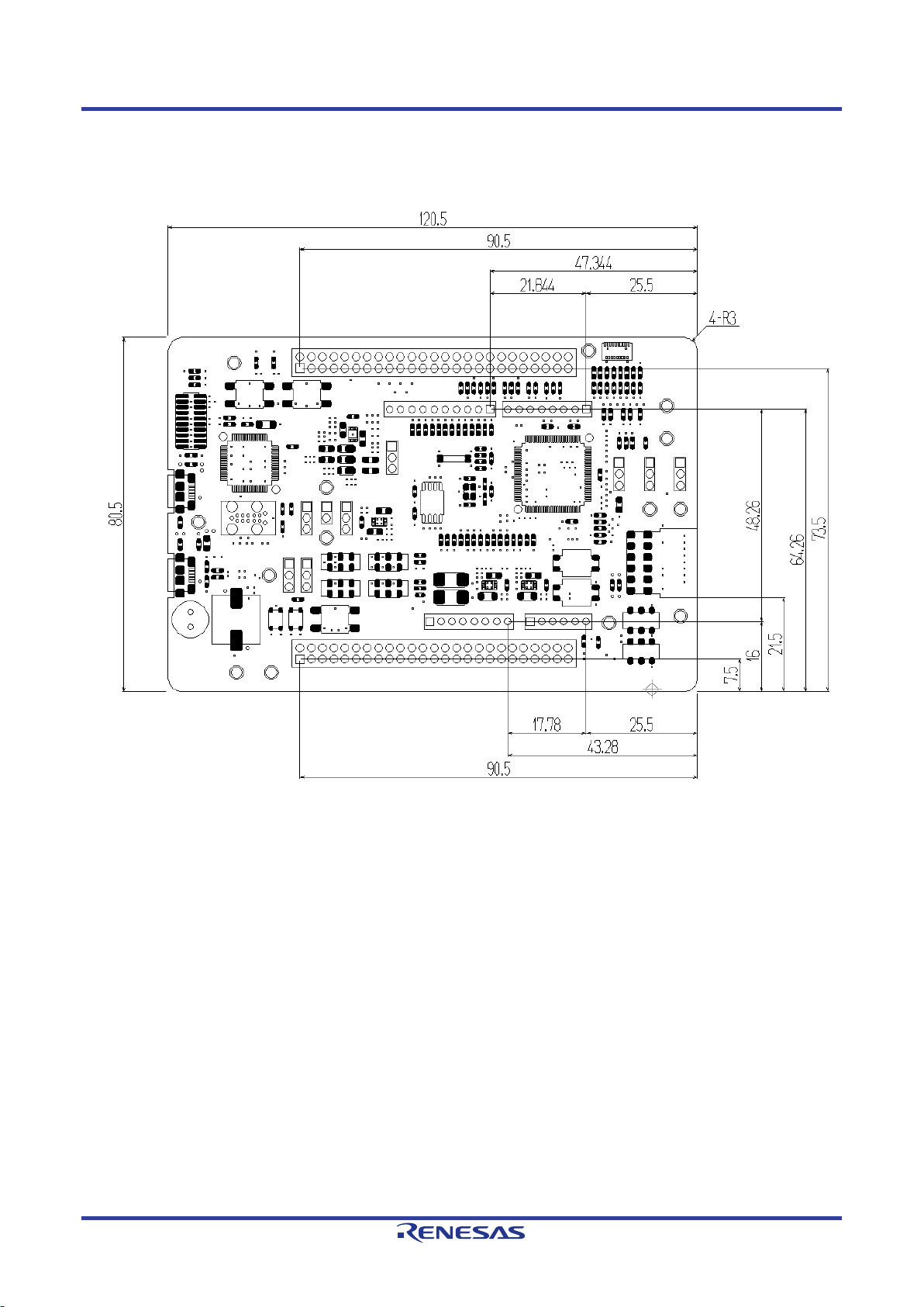
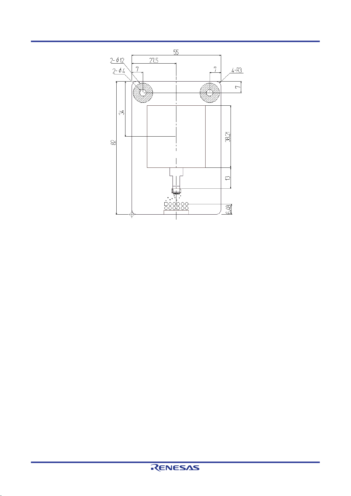
2.2 Board Dimensions
Figure 2-3 and Figure 2-4 below show the board dimensions and connector positions. All the through-hole
connectors are on a common 2.54 mm pitch grid for easy interfacing.
Figure 2-3: Main Board Dimensions (Unit: mm)
R20UT4801EJ0102 Rev.1.02 Page 15 of 95
Apr 16, 2021
Page 16
Evaluation Kit RE01 256KB 2.Board Layout
Figure 2-4: MIP-LCD Expansion Board Dimension (Unit: mm)
R20UT4801EJ0102 Rev.1.02 Page 16 of 95
Apr 16, 2021
Page 17
Evaluation Kit RE01 256KB 2.Board Layout
R1
R10
R11
GND2
LED 0
LED 1
J2
GND1
CN1
R2
R3
R4
R5
R6
R7
R8
R9
SW1 SW2
R12
R13
R14
R15
R16
R17
R18
R19
R20
R21
R22
R23
R24
R25
R26
R27
R28
R29
R30
R31
R32
R33
R39
R40 C1
C2
C3
L1
J3
J4
R34
R35
R36
R37
R38
T1
U2
C6
R41
R42
R43
R44
R45
R46
R48
R49
R50
R51
R52
R53
R47
C4 C5
CN2
POW ER1
C9
U6
R57
L2
L3
D1
D2
D3
R59
L4
X1
C8
R58
R61
C10
R60
U1
C7
R54
R55
R56
T2
C12
J5
J6
J7
C15
T4
T5
USB1
J-Link_
10pin_Needle
R68 R86
GND3
C19
L6
LED 2 R69
R66
J8
J9
J10
T3
T6
L5
U3
C16
C18
C13
R67
U7
C11
X2
C14
R62
R63
R64
C17
R71
R72
R73
R74
R75
R76
R77
R78
R79
R80
R81
R82
R83
R84
R85
R70
R87
R88
R89
R90
PMOD1
USB2
C22
C26
R91
R92
T7
J11
J12
SW3 SW4
SW5 SW6
C20
C21
R93
R94
C29
C25
C30
C23
C31
U5
L7
C24
U4
L8
C32
C27
C28
BT1
BT2
R95
SW7 S W8
RES
J13 J14
T8
GND4
J1
T9
T10
R98
R97
SW9
SW10
SW11
SW12
J15
2.3 Component Placement
Figure 2-5, Figure 2-6, and Figure 2-7 show placement of individual components of Evaluation Kit
Component types and values are shown on the board schematics.
.
Figure 2-5: Main Board Component Placement (Top-Side View)
R20UT4801EJ0102 Rev.1.02 Page 17 of 95
Apr 16, 2021
Page 18
Evaluation Kit RE01 256KB 2.Board Layout
J2
R99
R10 0
R10 5 R106
R10 4
R10 3
R10 2
R10 1
C33
R11 0
R10 9
R10 8
R10 7
C35
R11 2
C34
C37
R11 1
C36
C38
C39
C40
R11 3
R11 4
R11 5
R11 6
R11 7
R11 8
R12 2
R11 9
R12 0
R12 3
R12 4
R12 6
R12 8
R13 0
R13 1
R13 3
R13 4
R12 9
R12 7
R12 5
R12 1
R13 2
C41
C42
C43
U8
R135
R138
R13 7
C44
R13 6
J1
Figure 2-6: Main Board Component Placement (Bottom-Side View)
R20UT4801EJ0102 Rev.1.02 Page 18 of 95
Apr 16, 2021
Page 19
Evaluation Kit RE01 256KB 2.Board Layout
CN1
PMOD1
Figure 2-7: MIP-LCD Component Placement (Top-Side View)
R20UT4801EJ0102 Rev.1.02 Page 19 of 95
Apr 16, 2021
Page 20
Evaluation Kit RE01 256KB 2.Board Layout
Item
Function
Setting
SW3, SW5
Operation mode setting
(Emulator setting)
1-2, 5-6: short
Normal mode (using J-LinkTM OB)
SW4, SW6
Operation mode setting
1-2, 5-6: short
Normal mode
SW9
Start-up mode setting
1-2: short
Normal start-up
SW10
2-3: short
SW11,
SW12
Internal LDO setting
1-4: OFF
2-3: OFF
Internal LDO use
J5
Reference voltage generation
circuit setting
1-2: short
Reference voltage generation circuit not
used
J6
IOVCC0 power supply setting
1-2: short
Use output voltage from DCDC converter
J7
IOVCC1 power supply setting
1-2: short
Use output voltage from DCDC converter
J8
Operation mode setting
1-2: short
Normal operation
J9
Current measurement setting
1-2: short
Current measurement not performed
J10
Operation mode setting
1-2: short
Normal start-up
J11
Supercapacitor charging
method selection
1-2: short
Charge from external power supply
J12
Secondary battery selection
2-3: short
Supercapacitor
J15
Operation mode setting
1-2: short
Normal start-up
J8: 1-2 short
J9: 1-2 short
J10: 1-2 short
J11: 1-2 short
J12: 2-3 short
J15: 1-2 short
J7: 1-2 short
J6: 1-2 short
J5: 1-2 short
SW11: 1-4 OFF
2-3 OFF
SW12: 1-4 OFF
2-3 OFF
SW9: 1-2 short
SW10: 2-3 short
SW3: 1-2, 5-6 short
SW5: 1-2, 5-6 short
SW4: 1-2, 5-6 short
SW6: 1-2, 5-6 short
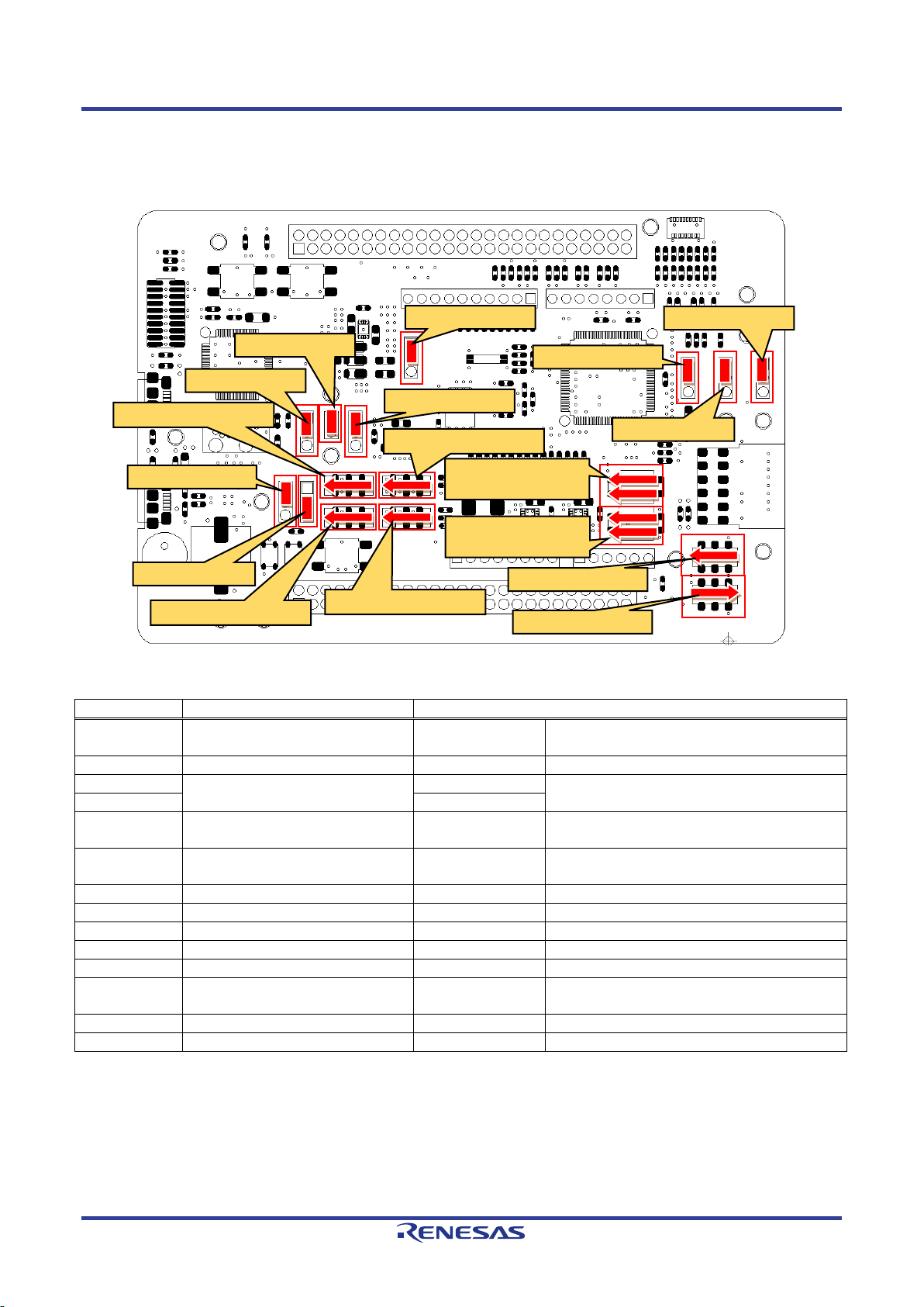
2.4 Board Initial Settings
The switch settings of the default kit configuration are as follows. The component layout is shown in Figure
2-8 and the detailed settings are shown in Table 2-1.
Figure 2-8: Component Layout and Settings
Table 2-1: Board Initial Settings
R20UT4801EJ0102 Rev.1.02 Page 20 of 95
Apr 16, 2021
Page 21
Evaluation Kit RE01 256KB 3.Internal Board Connections
Arduin o UNO Header
(J3,J4,J13,J14)
RE01-25 6KB
IOVCC IOVC C0 IOV CC1 AVCC0 V REFH0
J-LinkTM OB
Emula tor Con nector(CN2 )
Micro -B Connector
(US B2)
USB-UART Circuit
USB-UART IC
(U8)
Flash Memory (U7)
MIP-LCD E xpansi on Boar d Inte rface ( PMOD1)
MIP-LCD(P arallel ) Interf ace (CN 1)
VCC/ IOVCC to VCLH
Voltag e Regulator
VCC/ IOVCC to VCL
Voltag e Regulator
: Signal Line
R
: Resisto r
R
: Resistor(Do no fit)
SSW
: Slide switch
VCC/IOVCC to 3.3V
Voltag e Regulator
SW3, SW5
R
R
R
R
SPI0/1
SWD, RESn
DCDC_Ext_EN
DCDC_EHC_EN
R
QSPI
SC I0
R
User LE DS (LED0, LED 1)
R
IO
Analog IO
IO
MLCD
IIC0/1
IIC0/1
IIC0/1
Analog VREF
R
IO
IO
P000
P001
P002
P003
P004
P005
IO(IOVCC):
Analog IO:
SDA P012
SCL P 013
IIC0/1
(IOVCC0):
CLK P 011
SSL P015
MOSI P 010
MISO P815
SPI0/1:
(IOVCC0):
P409
IO(IOVCC1):
P204
P205
P302
P314
P315
P602
P603
P604
SWCL K P411, SWDIO P207
TXD P7 02, RXD P702, C TS P704, RTS P202
IO: P210,P410
SPCLK P011, SS L P015, MOSI P010, MISO P815
QSPC LK P812, QSS L P807, QIO P80[ 8:11]
IO: P508,P509
SCLK P111, VCOM P113, ENBS P1 09,
XRST P1 12, DATA P10 [0:7],
DEN P110, ENBG P108
P204 P 205 P302 P314 P3 15 P602 P60 3 P604
P000 P 001 P002 P003 P0 04 P005
P409
VR EF
(VREFH0)
VR EFH0
VR EFH0
SDA P012
SCL P 013
P208
P209
User Switches (SW1,SW2)
Contr ol MCU
(U6)
Micro -B Connector
(US B1)
SSW
R
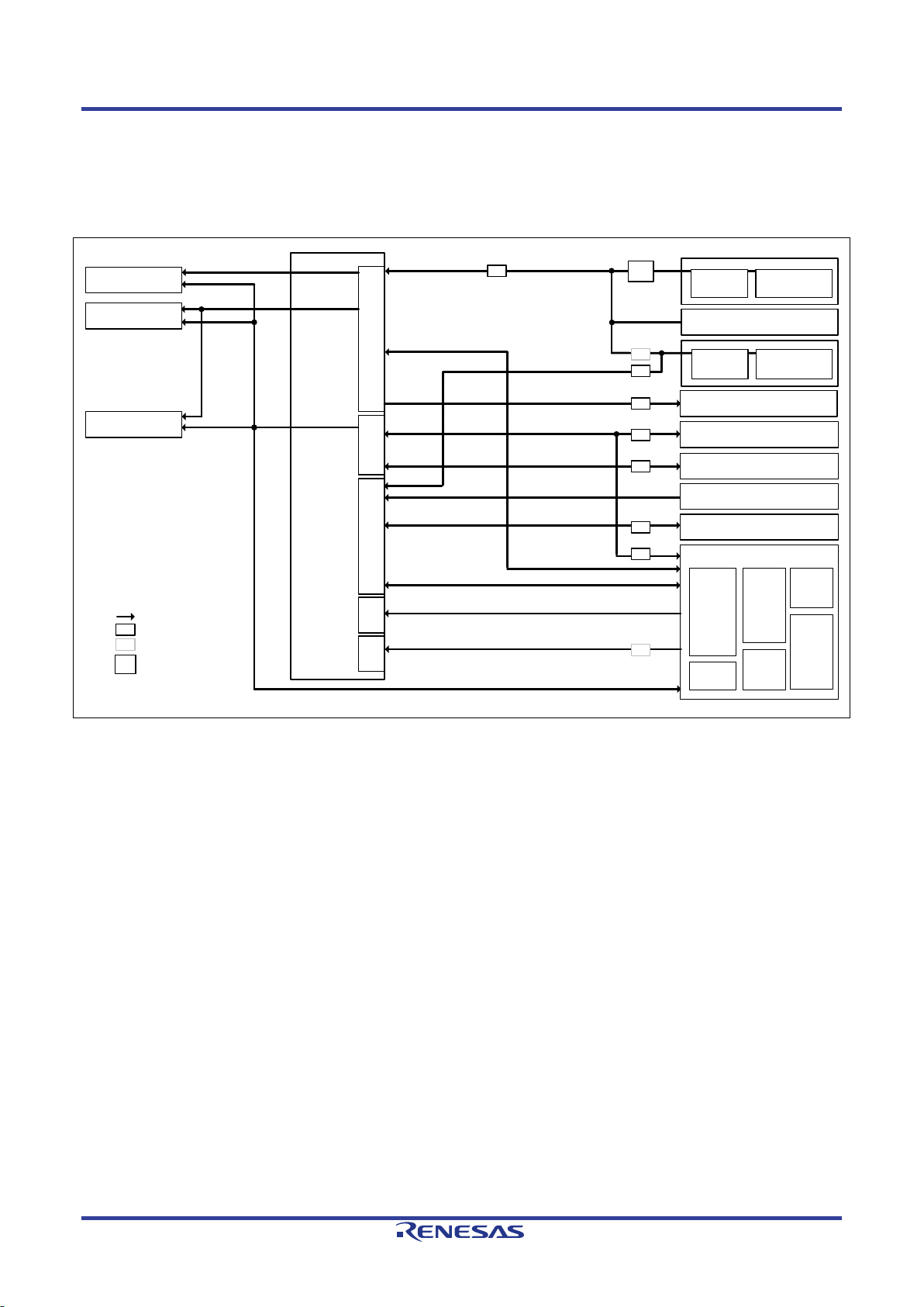
3.Internal Board Connections
Figure 3-1 shows the connectivity between Evaluation Kit and RE01. The pin connections are listed in Table
3-1 and Table 3-2.
Figure 3-1: Internal Board Block Diagram
R20UT4801EJ0102 Rev.1.02 Page 21 of 95
Apr 16, 2021
Page 22
Evaluation Kit RE01 256KB 3.Internal Board Connections
RE01
Main board
XTAL - 12
-
IOVCC
XCOUT - 9
-
IOVCC
SW1
P509
74
J2-24
IOVCC1
LED
LED0
P210
32
J1-32
IOVCC
PMOD*
PMOD_SSLA1_B_P015
P015
92
J2-42
IOVCC0
PMOD_MISOA_B_CTS4_C
P815
98
J2-48
IOVCC0
PMOD_INT_AGTWOA1_B_P814
P814
99
J2-49
IOVCC0
PMOD_IO0_P014
P014
93
J2-43
IOVCC0
USB-Serial
USB_SCI_TXD
P703
40
J1-40
IOVCC
USB_SCI_CTS
P704
39
J1-39
IOVCC1
MIP-LCD
MLCD_VCOM
P113
56
J2-6
IOVCC1
MLCD_XRST
P112
57
J2-7
IOVCC1
MLCD_SI6
P101
70
J2-20
IOVCC1
MLCD_SI4
P103
68
J2-18
IOVCC1
MLCD_SI2
P105
66
J2-16
IOVCC1
MLCD_SI0
P107
64
J2-64
IOVCC1
MLCD_SCLK
P111
58
J2-8
IOVCC1
Table 3-1: List of RE01 functions, pin number and header connections(1/2)
Category Function Port
Clock EXTAL - 13 - IOVCC
XCIN - 10 - IOVCC
Switch RES RES# 23 J1-23 IOVCC
SW2 P508 75 J2-25 IOVCC1
LED1 P410 17 J1-17 IOVCC
PMOD_MOSIA_B_P010 P010 97 J2-47 IOVCC0
PMOD_RSPCKA_B_P011 P011 96 J2-46 IOVCC0
PMOD_RESET_RXD4_C P813 100 J2-50 IOVCC0
PMOD_IO1 P806 7 J1-7 IOVCC0
Pin No.
Pin header
Power Domain
USB_SCI_RXD P702 41 J1-41 IOVCC
USB_SCI_RTS P202 38 J1-38 IOVCC1
MLCD_ENBS P109 60 J2-10 IOVCC1
MLCD_SI7 P100 71 J2-21 IOVCC1
MLCD_SI5 P102 69 J2-19 IOVCC1
MLCD_SI3 P104 67 J2-17 IOVCC1
MLCD_SI1 P106 65 J2-15 IOVCC1
MLCD_DEN P110 59 J2-9 IOVCC1
MLCD_ENBG P108 61 J2-11 IOVCC1
*: Please refer to Section 8.5 Pmod™ Interface for the relationship with the pin number of the PMOD connector.
R20UT4801EJ0102 Rev.1.02 Page 22 of 95
Apr 16, 2021
Page 23
Evaluation Kit RE01 256KB 3.Internal Board Connections
RE01
Main board
QSPI_QIO1_A
P810 3 J1-3
IOVCC0
QSPI_QIO0_A
P811 2 J1-2
IOVCC0
QSPI_QIO3_A
P808 5 J1-5
IOVCC0
ARDUINO_IO9_GTIOC2A_B
P302
48
J1-48/J3-2
IOVCC1
ARDUINO_MOSIA_B
P010
97
J2-47/J3-4
IOVCC0
ARDUINO_RSPCKA_B
P011
96
J2-46/J3-6
IOVCC0
ARDUINO_SDA0*
P012
95
J2-45/J3-9
IOVCC0
Arduino
ARDUINO_IO0_RXD5_B
P314
45
J1-45/J4-1
IOVCC1
ARDUINO_IO2_IRQ7_B
P204
36
J1-36/J4-3
IOVCC1
ARDUINO_IO4
P602
53
J2-3/J4-5
IOVCC1
ARDUINO_IO6_GTIOC5B_B
P604
51
J2-1/J4-7
IOVCC1
Arduino
IOVCC0/IOVCC1/
RESn
RES#
23
J1-23/ J13-3
IOVCC
Board_5V
- - J13-5
-
Arduino
ARDUINO_AN000
P000
89
J2-49/J14-1
AVCC0
ARDUINO_AN002
P002
87
J2-37/J14-3
AVCC0
ARDUINO_AN004
P004
85
J2-35/J14-5
AVCC0
Table 3-2: List of RE01 functions, pin number and header connections (2/2)
Category Function Port
Flash
Memory
Arduino
UNO (J3)
UNO (J4)
QSPI_QSSL_A P807 6 J1-6 IOVCC0
QSPI_QIO2_A P809 4 J1-4 IOVCC0
QSPI_QSPCLK_A P812 1 J1-1 IOVCC0
ARDUINO_IO8 P409 18 J1-18/J3-1 IOVCC
ARDUINO_SSLA1_B P015 92 J2-42/J3-3 IOVCC0
ARDUINO_MISOA_B P815 98 J2-48/J3-5 IOVCC0
ARDUINO_VREF** - 84 J3-8 VREFH0
ARDUINO_SCL0* P013 94 J2-44/J3-10 IOVCC0
ARDUINO_IO1_TXD5_B P315 44 J1-44/J4-2 IOVCC1
Pin No.
Pin header
Power Domain
ARDUINO_IO3_IRQ8_C P205 35 J1-35/J4-4 IOVCC1
ARDUINO_IO5_GTIOC5A_B P603 52 J2-2/J4-6 IOVCC1
ARDUINO_IO7 P300 50 J1-50J4-8 IOVCC1
UNO (J13)
UNO (J14)
*: The default kit configuration uses a transfer rate of 50kbps or less. To increase the transfer rate, change the resistor
values (R21, R22).
**: Not connected by default. Please change the resistor based on your application.
IOVCC0**/IOVCC1/AVCC0** - 91/46/78 J13-1
LP_3V3 - - J13-2 -
LP_3V3 - - J13-4 -
VCC_MCU - 14 J1-14/J13-8 IOVCC
ARDUINO_AN001 P001 88 J2-48/J14-2 AVCC0
ARDUINO_AN003 P003 86 J2-36/J14-4 AVCC0
ARDUINO_AN005 P005 82 J2-32/J14-6 AVCC0
AVCC0
R20UT4801EJ0102 Rev.1.02 Page 23 of 95
Apr 16, 2021
Page 24
Evaluation Kit RE01 256KB 4.Power Supply
RE01-25 6KB
IOVCC
5.0V to 3. 3V
Voltag e Regulator
EHC
VCC/ IOVCC
IOVC C0
IOVC C1 AVCC0 V REF H0
R
R
R
CC
Contr ol MCU
(U6)
Micro -B Connector
(US B1)
J-LinkTM OB
Emula to r Connect or
(CN2 )
Micro -B Connector
(US B2)
USB-UART Circuit
USB-UART IC
(U8)
Flash Memory
(U7)
USER S witches
(SW1, SW2)
MIP-LCD E xpans ion Boar d Inte rface
(PMO D1)
MIP-LCD(P arallel) Int erface
(CN1)
IOVC C0
IOVC C1
Arduin o UNO Header
(J3,J4,J13,J14)
5.0V
R
R
R
R
MCU
VCC/ IOVCC to VCLH
Voltag e Regulator
VCC/ IOVCC to VCL
Voltag e Regulator
R
R
UC_ VCC
VCC_ MCU
VCC_ MCU
UC_ VCC
VR EFH0
5.0V
J8
J10
J6
J7
J5
SSW
SSW
VCC/IOVCC to 3.3V
Voltag e Regulator
J15
SW11
SW12
R
J9
: Power Line
R
: Resisto r
R : Resistor(Do no fit)
C
: Cap acitor
: Jum per sw itch
: T hrough ho le
SSW
: Slide swit ch
LP_P RODUCT_3V3
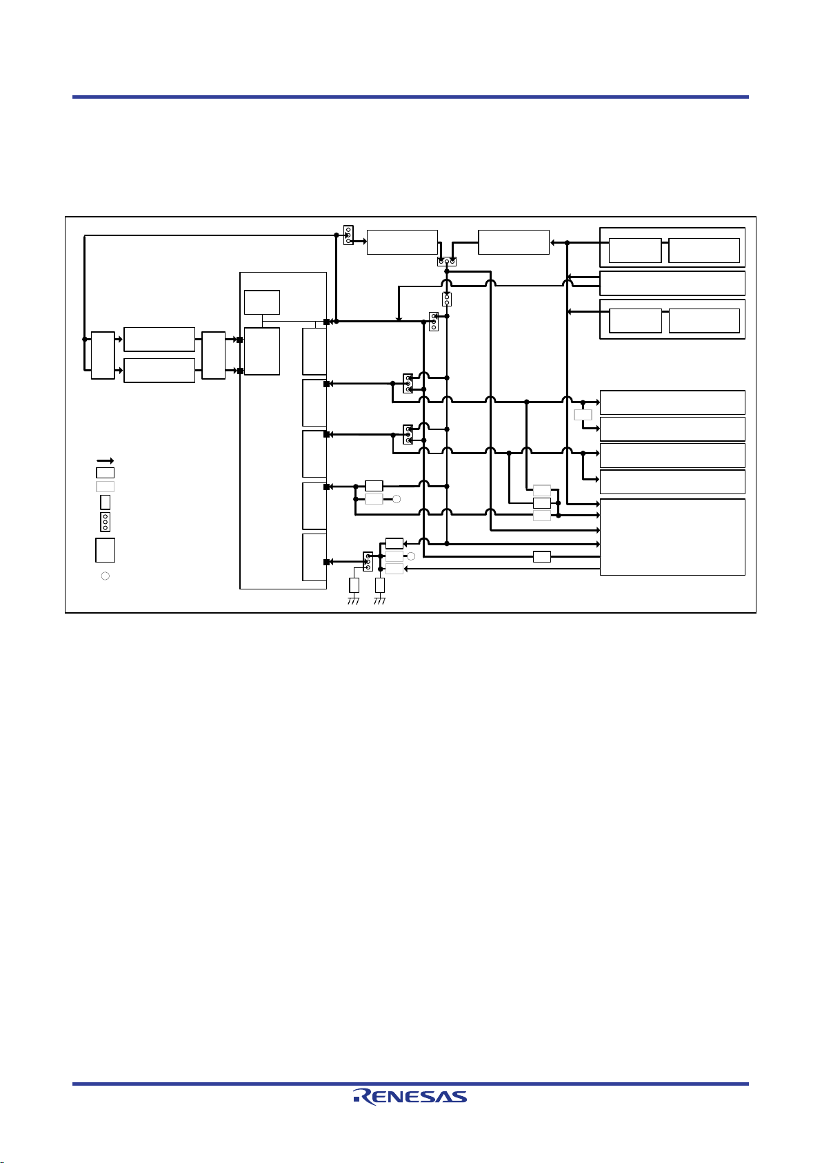
4. Power Supply
4.1 Power Supply System
Figure 4-1 shows power supply system diagram of Evaluation kit.
Figure 4-1: Power Supply System Diagram
R20UT4801EJ0102 Rev.1.02 Page 24 of 95
Apr 16, 2021
Page 25
Evaluation Kit RE01 256KB 4.Power Supply
Source
Supply voltage
Supply current
I-jetTM (CN2)
5V
Maximum 420mA
J-LinkTM OB (USB1)
5V
Maximum 500mA
J-LinkTM (CN2)
5V
Maximum 300mA
E2 (CN2)
3.3V
Maximum 200mA
USB serial (USB2)
5V
Maximum 500mA
Emulator
Emulator connector (CN2)
J-LinkTM OB connector (USB1)
USB cable
USB serial connector (USB2)
USB cable
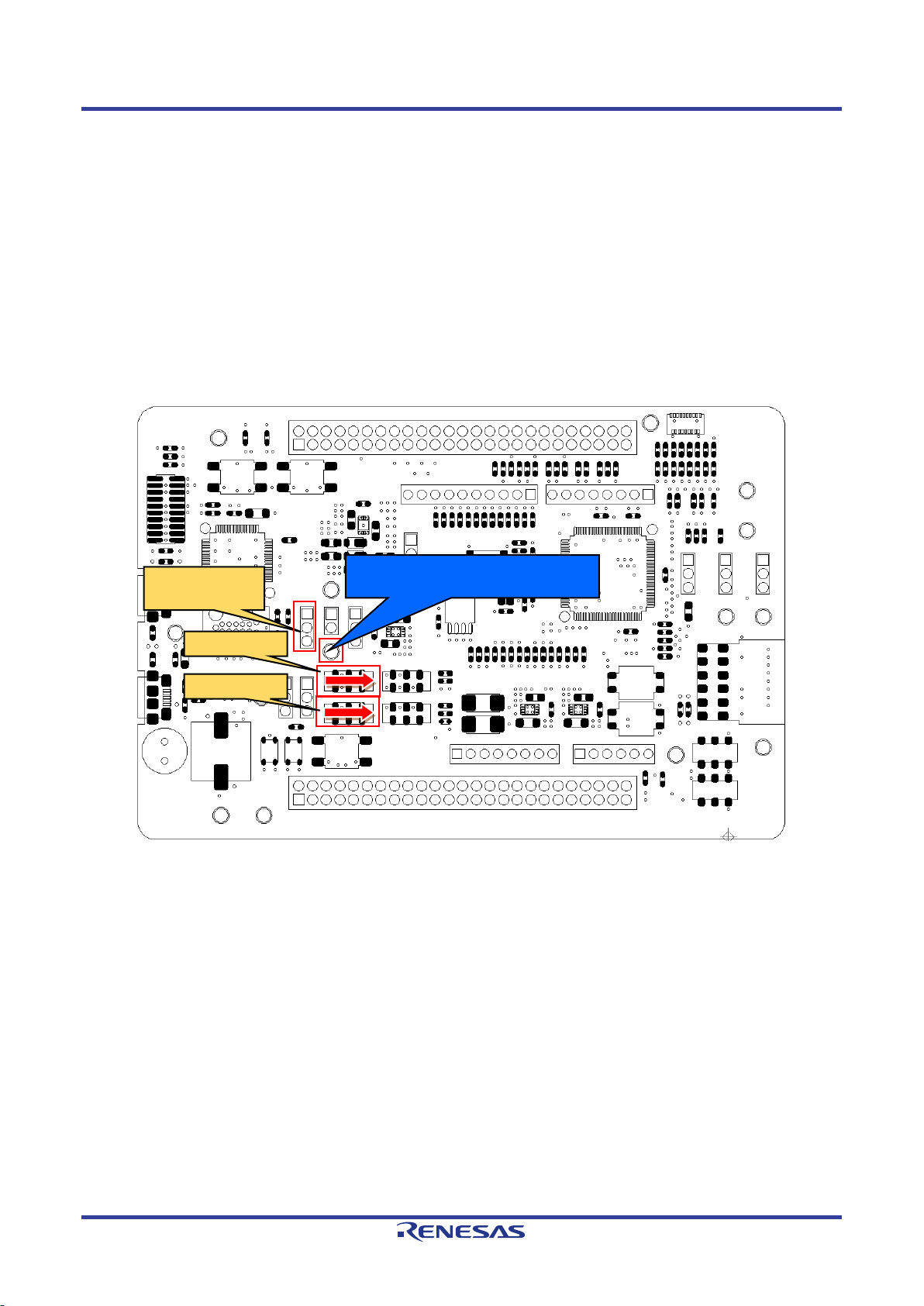
4.2 Power Supply Source
Evaluation Kit is supplied by emulator through USB cable. The details of power supply components are
shown in Figure 4-2 and Table 4-1. When the Evaluation Kit is connected to another system then that system
should supply power to the Evaluation Kit.
When operating in stand-alone mode, connect a USB cable to USB1 or USB2 and supply the voltage
through VBUS. At that time, do not use J-Link
TM
OB or USB serial function.
Figure 4-2: Components Layout (power supply)
Table 4-1: Power Supply Specifications
R20UT4801EJ0102 Rev.1.02 Page 25 of 95
Apr 16, 2021
Page 26
Evaluation Kit RE01 256KB 4.Power Supply
J8: 1-2 open
Current Measurement Point
SW3: EHC
SW5: EHC
4.3 External Power Supply
It is possible to supply voltage to RE01 power terminal by using external power supply. This allows the entire
or individual power domain to operate at any voltage (1.62 – 3.6V). Normally, the emulator supplies voltage
equivalent to 3.3V, which is the voltage value after reduction by the regulator. (excluding device which can
supply 3.3V)
4.3.1 All power pins
Figure 4-3 shows the component layout. Follow the steps below when supplying voltage from external p
supply to all RE01 power pins:
1. Set SW3 and SW5 to EHC.
2. Open J8 jumper pin 1-2 and 2-3.
3. Supply voltage (1.62V-3.6V) from pin 2 of J8 or T6 using an external power supply.
ower
2-3 open
Figure 4-3: Component Layout and Setting (External Power Supply)
Keep the following in mind when using this feature:
• Debugging using J-Link OB is not possible. Please use another emulator. For details on the other
emulators, refer to chapter 6 Debug.
• When using the E2 emulator, do not supply power from the emulator.
(T6)
R20UT4801EJ0102 Rev.1.02 Page 26 of 95
Apr 16, 2021
Page 27
Evaluation Kit RE01 256KB 4.Power Supply
IOVCC0(T4)
J6: 1-2 open
2-3 open
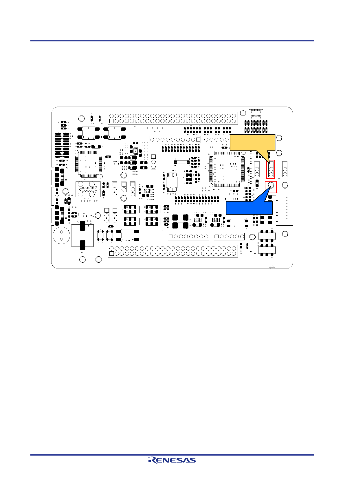
4.3.2 IOVCC0
Figure 4-4 shows the component layout. Follow the steps below when supplying voltage from external power
supply to IOVCC0 pin:
1. Open J6 jumper pin 1-2 and 2-3.
2. Supply voltage (1.62V – 3.6V) to any power supply pins other than IOVCC0 pin.
3. Supply voltage to T4.
Figure 4-4: Component Layout and setting (External Power Supply)
R20UT4801EJ0102 Rev.1.02 Page 27 of 95
Apr 16, 2021
Page 28
Evaluation Kit RE01 256KB 4.Power Supply
IOVCC1(T1)
J7: 1-2 open
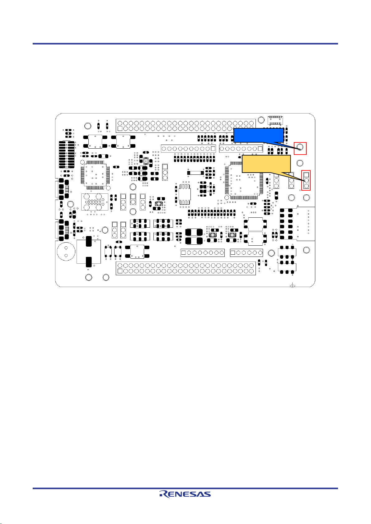
4.3.3 IOVCC1
Figure 4-5 shows the component layout. Follow the steps below when supplying voltage from external power
supply to IOVCC1 pin:
1. Open J7 jumper pin 1-2 and 2-3.
2. Supply voltage (1.62V – 3.6V) to any power supply pins other than IOVCC1 pin.
3. Supply voltage to T1.
2-3 open
Figure 4-5: Component Layout and Setting (External Power Supply)
R20UT4801EJ0102 Rev.1.02 Page 28 of 95
Apr 16, 2021
Page 29

Evaluation Kit RE01 256KB 4.Power Supply
AVCC0(T5)
4.3.4 AVCC0
The component layout are shown in Figure 4-6 and Figure 4-7. Follow the steps below when supplying
voltage from external power supply to AVCC0 pin:
1. Remove R108.
2. Fit R107.
3. Supply voltage (1.62V – 3.6V) to any power supply pins other than AVCC0 pin.
4. Supply voltage to T5.
Figure 4-6: Component Layout (External Power Supply (Top))
R20UT4801EJ0102 Rev.1.02 Page 29 of 95
Apr 16, 2021
Page 30

Evaluation Kit RE01 256KB 4.Power Supply
R108: removed
R107: fitted
Figure 4-7: Component Layout (External Power Supply (Bottom))
R20UT4801EJ0102 Rev.1.02 Page 30 of 95
Apr 16, 2021
Page 31

Evaluation Kit RE01 256KB 4.Power Supply
VREFH0(T2)
J5: 1-2 short
R54: removed
R55: removed
R56: fitted
4.3.5 VREFH0
The component layout and settings are shown in Figure 4-8. Follow the steps below when supplying voltage
from external power supply to VREF0 pin:
1. Remove R54 and R55
2. Fit R56.
3. Short J5 jumper pin 1-2.
4. Supply voltage (1.62V – AVCC0) to any power supply pins other than VREF0 pin.
5. Supply voltage to T2.
Figure 4-8: Component Layout and Settings (External Power Supply)
R20UT4801EJ0102 Rev.1.02 Page 31 of 95
Apr 16, 2021
Page 32

Evaluation Kit RE01 256KB 5.Operation/Start-up Mode
Component Name
Setting
SW3, SW5*1
1-2, 5-6
Normal Operation
*2
SW4, SW6
1-2, 5-6
Normal Operation
*2
SW3: Normal
SW5: Normal
SW4: Normal
SW6: Normal
5. Operation/Start-up Mode
Evaluation Kit for RE01 supports 2 operation and start-up modes: normal and energy harvesting (hereinafter,
EHC).
5.1 Normal Operation
In normal operation, power is supplied from emulator or external power supply. To use normal operation
mode, several switch settings must be made. The layout and details of the switch setting are shown in Figure
5-1 and Table 5-1.
Other settings will be as per the default kit configuration, as supplied.
Figure 5-1: Component Layout and Settings (Normal Operation)
Table 5-1: Configuration Details (Normal Operation)
*1
: Also depends on debug function used. For more information, refer to Section 6. Debug.
*2
: The settings are supported in default configuration, as supplied.
R20UT4801EJ0102 Rev.1.02 Page 32 of 95
Apr 16, 2021
Page 33

Evaluation Kit RE01 256KB 5.Operation/Start-up Mode
Component Name
Setting
J8
2-3
short
J10
1-2, 2-3
open
J15
2-3
short
SW3–SW6
2-3, 6-7
EHC
SW9
1-2
Startup*1
SW10
1-2
EHC
Component Name
Settings
J6
1-2
Supply voltage generated by DC/DC converter to IOVCC0 pin of RE01
2-3
Supply voltage generated by VCC/IOVCC pin of RE01 to IOVCC0 pin of
RE01
J7
1-2
Supply voltage generated by DC/DC converter to IOVCC1 pin of RE01
2-3
Supply voltage generated by VCC/IOVCC pin of RE01 to IOVCC1 pin of
RE01
IOVCC0 power selection
J8: 2-3 short
J10: 1-2 open
IOVCC1 power selection
SW3: EHC
SW5: EHC
SW4: EHC
SW6: EHC
SW10: EHC
SW9: Startup
J15: 2-3 short
5.2 EHC Operation
RE01 supports energy harvesting function. In EHC operation, the power is supplied from the included solar
panel. User circuit can start operating when voltage is supplied to VSC_VCC pin of RE01.
Switch settings are required to operate the energy harvesting function. The related component layout and
setting details are shown in Figure 5-2, Table 5-2, and Table 5-3. For more information of energy
control circuit for RE01 specifications, refer to RE01 Group User’s Manual’s Hardware.
switch (J7)
2-3 open
switch (J6)
harvesting
Other settings will be as per the default kit configuration, as supplied.
Figure 5-2: Component Layout and Settings (EHC Operation)
Table 5-2: Configuration Details (EHC Operation)
*1
: The setting is supported in default configuration, as supplied.
Table 5-3: Switch Details (J6, J7)
R20UT4801EJ0102 Rev.1.02 Page 33 of 95
Apr 16, 2021
Page 34

Evaluation Kit RE01 256KB 5.Operation/Start-up Mode
RE01-25 6KB
IOVCC IOVC C0 I OVCC1
J-LinkTM OB
Emula tor Con nector(CN2 )
Micro -B Connector
(US B2)
USB-UART Circuit
USB-UART IC
(U8)
: Signal Line
R
: Resisto r
R : Resistor(Do no fit)
SSW
: Slide switch
VCC/IOVCC to 3.3V
Voltag e Regulator
SW3, SW5
EHC
(Ope n)
R
R
SWD, RESn
DCDC_EHC_EN
SC I0
IIC0/1
SWCL K P411, SWDIO P207
SDA P012
SCL P 013
P209
Contr ol MCU
(U6)
Micro -B Connector
(US B1)
R
Boot
Startu p (Single chip)
Norm al
EHC
MD
EHMD
SW9
SW10
RE01-25 6KB
IOVCC
5.0V to 3. 3V
Voltag e Regulator
EHC
VCC/ IOVCC
IOVC C0 IOV CC1 AVCC0 VR EFH0
R
R
R
CC
Flash Memory
(U7)
USER S witches
(SW1, SW2)
MIP-LCD E xpansi on Boar d Inte rface
(PMO D1)
MIP-LCD(P arallel) Int erface
(CN1)
IOVC C0
IOVC C1
Arduin o UNO Header
(J3,J4,J13,J14)
5.0V
R
R
R
R
MCU
R
R
UC_ VCC
VCC_ MCU
VCC_ MCU
UC_ VCC
VR EFH0
J8 2-3 sho rt
J10
Open
J6
1-2 sho rt
VCC/IOVCC to 3.3V
Voltag e Regulator
J15
2-3 sho rt
R
J9
short
: Power Line
R
: Resisto r
R : Resistor(Do no fit)
C
: Cap acitor
: Jum per sw itch
: Thro ugh ho le
SSW
: Slide swit ch
LP_P RODUCT_3V3
Ext_DCDC
Emula tor or
USB
VSC_VCC
VBAT_EHC
SW4 EHC
SW6 EHC
VC C_SU
UC_ VCC
T10
BT1 o r
BT2
J7
1-2 sho rt
J5
1-2 sho rt
Figure 5-3: Block diagram of Signal line (EHC Operation)
Figure 5-4: Block diagram of Power line (EHC Operation)
R20UT4801EJ0102 Rev.1.02 Page 34 of 95
Apr 16, 2021
Page 35

Evaluation Kit RE01 256KB 5.Operation/Start-up Mode
Solar Panel Interface (T9, T10)
RE01
RE01
Port
Pin
Port
Pin
T9
GROUND
-
-
T10
-
VSC_VCC
29
Solar panel interface
Solar panel interface
Solar panel
5.2.1 Solar Panel
This product is equipped with solar panel interface (T9, T10). The component layout and details are
displayed in Figure 5-5 and Table 5-4. Connect the included solar panel to T9 and T10 using the attached IC
clip.
(T9)
(T10)
Figure 5-5: Component Layout (EHC Operation)
Table 5-4: Solar Panel Interface
Pin
Name
Pin Name
R20UT4801EJ0102 Rev.1.02 Page 35 of 95
Apr 16, 2021
Page 36

Evaluation Kit RE01 256KB 5.Operation/Start-up Mode
Component Name
Setting
J12
1-2
External battery
2-3
Supercapacitor
Component Name
Setting
J11
1-2
Charging from external power supply
2-3
Charge by using board voltage
Supercapacitor (BT2)
Interface for external
battery(BT1)
Charging method selection switch
Battery selection switch (J12)
Charging Terminal (T7)
5.2.2 Supercapacitor / External Battery
Supercapacitor / external battery can be connected to VBAT_EHC pin in RE01. Switch settings are required
in order to use supercapacitor / external battery. Component layout and configuration details are shown in
Figure 5-6 and Table 5-5.
(J11)
Figure 5-6: Component Layout (EHC Operation)
Table 5-5: Switch Configuration(J12)
When using supercapacitor, the supercapacitor itself may need to be charged because it may have been
discharged. There are 2 charging methods that can be selected through switch setting. The related
component layout and settings are shown in Figure 5-6 and Table 5-6.
When charging, use J12 in the open setting.
• Charging from external power supply
Connect a stabilized power supply to the charging
terminal (T7).
• Charging from the voltage converted on board supplied by an emulator
Connect an emulator to CN2 port or a USB cable to USB1/USB2 port.
Set the charging voltage (2.6V or 3.0V) to the value specified in Secondary Battery (VBAT) Charging Voltage
Select Bit (VBATSEL) in Option Function Select Register 1 (OFS1).
Table 5-6: Switch Configuration(J11)
Set J11 to 1-2 after charging is completed.
R20UT4801EJ0102 Rev.1.02 Page 36 of 95
Apr 16, 2021
Page 37

Evaluation Kit RE01 256KB 5.Operation/Start-up Mode
External Battery (BT2)
RE01
RE01
Port
Pin
Port
Pin
1 - VBAT_EHC
28
2
GROUND
-
-
Storage Capacitor (C29)*
Storage Capacitor (C25)
Storage Capacitor (C30)
Make sure that the external battery is already installed before selecting the external battery. The component
layout and setting are described in Figure 5-6 and Table 5-7.
1
The recommended external battery is SLB Series (Nichicon). Because the included solar panel*
generates
42µA, it might take time to charge the recommended external battery, depending on the operation setting of
RE01. Depending on your evaluation
1
: Panasonic AM-1815CA operating voltage 3.0 V, operating current 42.0µA (white fluorescent lamp-
*
200lx(25
o
C))
content, consider charging before mounting.
Table 5-7: External Battery (BT2)
Pin
Signal Name
Pin Signal Name
5.2.3 Storage Capacitor
RE01 has a 200uF capacitor connected to the VCC_SU pin. Depending on your board environment, it may
be necessary to change the capacitor’s capacitance connected to VCC_SU pin. If necessary, mount a
capacitor on C29 (size: 1608). Component layout is shown in Figure 5-7. For more information about storage
capacitor specifications, refer to RE01 Group User’s Manual’s Hardware.
*
: DNF
5.2.4 DC/DC Converter Control
DC/DC converter must be enabled to supply the voltage to the user circuit when using energy harvesting
function. To enable DC/DC converter, output a high level from P209 and make sure that there is enough
charging voltage in external battery/supercapacitor. This voltage equals to the value of VBATSEL setting
(2.6V or 3.
0V).
R20UT4801EJ0102 Rev.1.02 Page 37 of 95
Apr 16, 2021
Figure 5-7: Component Layout (EHC Operation)
Page 38

Evaluation Kit RE01 256KB 5.Operation/Start-up Mode
Component Name
Setting
J6, J7
1-2
short
J12
2-3
short
J6: 1-2 short
J7: 1-2 short
J12: 2-3 short
Solar Panel Interface
Solar Panel Interface
5.2.5 How to Use
5.2.5.1 When Operating Peripheral Circuits after Steady Operation Period
Follow the steps below to operate peripheral circuits after EHC steady operation period. The settings below
are intended for the case where supercapacitor (charged) is used. The program has to be downloaded to
RE01 internal flash memory in advance.
Sample code is also available on Renesas website, entitled “Maintenance free power management by RE
energy harvesting controller (R01AN4837)”.
1. Follow the setting shown in Figure 5-2 and Table 5-2.
2. Follow the setting shown in Figure 5-8 and Table 5-8.
3. Connect the solar panel to the solar panel interface (T9 and T10).
(T9)
(T10)
Figure 5-8: Component Layout and Settings (EHC Operation)
Table 5-8: Configuration Details (EHC Operation)
The settings in the table above are supported in default configuration, as supplied.
R20UT4801EJ0102 Rev.1.02 Page 38 of 95
Apr 16, 2021
Page 39

Evaluation Kit RE01 256KB 5.Operation/Start-up Mode
Component Name
Setting
J6
2-3
short
J7
1-2
short*1
J12
2-3
short*1
J6: 2-3 short
J7: 1-2 short
PMOD Connector
(
J12: 2-3 short
Solar Panel Interface
Solar Panel Interface
5.2.5.2 When using the MIP-LCD Expansion Board During Secondary Battery Charging Period
Follow the steps below to operate MIP LCD expansion board during secondary battery charging period. The
setting below are intended for the case where supercapacitor (charged) is used. The program has to be
downloaded to RE01 internal flash memory in advance.
Sample code is also available on Renesas website, entitled “Energy harvesting launch operation and quick
start SMIP display
demo using Evaluation Kit RE01 256KB (R01AN5406)”.
1. Follow the settings shown in Figure 5-2 and Table 5-2.
2. Follow the settings shown in Figure 5-9 and Table 5-9.
3. Connect MIP-LCD expansion board to the PMOD connector (PMOD1). (Refer to Section 8.5.1 MIP-LCD
Expansion Board for more details).
4. Connect the solar panel to solar panel interface (T9, T10).
(T9)
(T10)
Figure 5-9: Component Layout and Settings (EHC Operation)
Table 5-9: Configuration Details (EHC Operation)
*1
: The settings are supported in default configuration, as supplied.
PMOD1)
R20UT4801EJ0102 Rev.1.02 Page 39 of 95
Apr 16, 2021
Page 40

Evaluation Kit RE01 256KB 5.Operation/Start-up Mode
Component Name
Setting
J6
1-2
short*1
J7
2-3
short
J12
2-3
short*1
J6: 1-2 short
J7: 2-3 short
MIP-LCD Connector(CN1)
J12: 2-3 short
Solar Panel Interface
Solar Panel Interface
5.2.5.3 When using Parallel MIP-LCD during Secondary Battery Charging Period
Follow the steps below to operate parallel MIP LCD during secondary battery charging period. The setting
below are intended for the case where supercapacitor (charged) is used. The program has to be downloaded
to RE01 internal flash memory in advance.
1. Follow the settings shown in Figure 5-2 and Table 5-2.
2. Follow the settin
gs shown in Figure 5-10 and Table 5-10.
3. Connect parallel MIP-LCD to the MIP-LCD connector (CN1). (Refer to Section 8.7 MLCD (Memory In
Pixel Liquid Crystal Display) Interface for more details).
4. Connect the solar panel to solar panel interface (T9, T10).
(T9)
(T10)
Figure 5-10: Component Layout and Settings (EHC Operation)
Table 5-10: Configuration Details (EHC Operation)
*1
: The settings are supported in default configuration, as supplied.
R20UT4801EJ0102 Rev.1.02 Page 40 of 95
Apr 16, 2021
Page 41

Evaluation Kit RE01 256KB 5.Operation/Start-up Mode
Discharge Switch (SW7)
Discharge Switch (SW8)
5.2.5.4 Discharge Switch (SW7, SW8)
Discharge switches are included in the main board. SW7 is used to discharge RE01 VCC/IOVCC power
supply line. SW8 is used to discharge storage capacitors (C25, C29, and C30). This discharge switches
must be used when the user uses energy harvesting function, operate the main board, then restart the
energy harvesting function again from the beginning. Press the discharge switches before using energy
harvesting function every time the energy harvesting function is started up from the beginning. The
discharge
switches are shown in Figure 5-11.
Figure 5-11: Component Layout (EHC Operation)
R20UT4801EJ0102 Rev.1.02 Page 41 of 95
Apr 16, 2021
Page 42

Evaluation Kit RE01 256KB 5.Operation/Start-up Mode
Switch Setting
Start-up Mode
MD (SW9)
EHMD (SW10)
1-2: short
1-2: short
Energy Harvest Start-up Mode
1-2: short
2-3: short
Normal Start-up Mode
*1
2-3: short
-*2
SCI/USB Boot Mode
Start-up Mode Switch (SW9)
Start-up Mode Switch (SW10)
1-2: short
2-3: short
5.3 RE01 Start-up Mode
RE01 supports 3 start-up modes. Switch settings are necessary to select the start-up mode. Component
layout and settings related to start-up modes are explained in Figure 5-12 and Table 5-11. For more details of
start-up modes for RE01, refer to RE01 Group User’s Manual’s Hardware.
Figure 5-12: Component Layout (RE01 Start-up Mode)
Table 5-11: Configuration Details (RE01 Start-up Mode)
*1
: The setting is supported in default configuration, as supplied.
*2
: Don't care
R20UT4801EJ0102 Rev.1.02 Page 42 of 95
Apr 16, 2021
Page 43

Evaluation Kit RE01 256KB 6.Debug
Supported Emulator
Chapter Reference
J-LinkTM OB
6.1, 6.5
J-LinkTM
6.2, 6.5
I-JetTM
6.2
E2
6.3, 6.4
J-LinkTM OB Connector (USB1)
J8: 1-2 short
J9: short
SW3: Normal
SW5: Normal
USB Cable
R71: Fitted
R72: Removed
R74: Fitted
R76: Removed
J10: 1-2 short
6. Debug
This board supports emulators as listed in Table 6-1.
Table 6-1: Supported Emulators
6.1 J-Link
This main board is equipped with Segger J-Link
included USB cable to this board and host PC.
6.1.1 Component Layout and Settings when using J-Link
When using J-Link
the component layout and detailed settings for using J-Link
configuration, as supplied.
Figure 6-2 and Figure 6-3 show the connection relationship between the power supply and signals in this
setting change.
TM
OB
TM
OB, several switch and resistor settings must be set. Figure 6-1 and Table 6-2 shows
TM
OB. RE01 debugging is possible by connecting the
TM
OB
TM
OB. This function is supported in the default
Other settings will be as per the default kit configuration, as supplied.
R20UT4801EJ0102 Rev.1.02 Page 43 of 95
Apr 16, 2021
Figure 6-1: Component Layout and Settings (J-Link
TM
OB)
Page 44

Evaluation Kit RE01 256KB 6.Debug
Component
Setting
SW3, SW5
1-2, 5-6
Normal
J8
1-2
short
J9 - short
J10
1-2
short
R71, R74
Fitted
R72, R76
Removed
Arduin o UNO Header
(J3,J4,J13,J14)
RE01-25 6KB
IOVCC IOVC C0 IOV CC1 AVCC0 V REFH0
J-LinkTM OB
Emula tor Con nector(CN2 )
Micro -B Connector
(US B2)
USB-UART Circuit
USB-UART IC
(U8)
Flash Memory (U7)
MIP-LCD E xpansi on Boar d Inte rface ( PMOD1)
MIP-LCD(P arallel ) Interf ace (CN 1)
VCC/ IOVCC to VCLH
Voltag e Regulator
VCC/ IOVCC to VCL
Voltag e Regulator
: Signal Line
R
: Resisto r
R : Resistor(Do no fit)
SSW
: Slide switch
VCC/IOVCC to 3.3V
Voltag e Regulator
SW3, SW5
Norm al setting
R
R
R
R
SPI0/1
SWD, RESn
DCDC_Ext_EN
DCDC_EHC_EN
R
QSPI
SC I0
R
User LE DS (LED0, LED 1)R
IO
Analog IO
IO
MLCD
IIC0/1
IIC0/1
IIC0/1
Analog VREF
R
IO
IO
P000
P001
P002
P003
P004
P005
IO(IOVCC):
Analog IO:
SDA P012
SCL P 013
IIC0/1
(IOVCC0):
CLK P 011
SSL P015
MOSI P 010
MISO P815
SPI0/1:
(IOVCC0):
P409
IO(IOVCC1):
P204
P205
P302
P314
P315
P602
P603
P604
SWCL K P411, SWDIO P207
TXD P7 02, RXD P702, C TS P704, RTS P202
IO: P210,P410
SPCLK P011, SS L P015, MOSI P010, MISO P815
QSPC LK P812, QSS L P807, QIO P80[ 8:11]
IO: P508,P509
SCLK P111, VCOM P113, ENBS P1 09,
XRST P1 12, DATA P10 [0:7],
DEN P110, ENBG P108
P204 P 205 P302 P314 P3 15 P602 P60 3 P604
P000 P 001 P002 P003 P0 04 P005
P409
VR EF
(VREFH0)
VR EFH0
VR EFH0
SDA P012
SCL P 013
P208
P209
User Switches (SW1,SW2)
Contr ol MCU
(U6)
Micro -B Connector
(US B1)
SSW
R
R71, R7 4 fitted
R72, R7 6
not fitted
TM
Table 6-2: Configuration Details (J-Link
OB)
The settings in the table above are supported in the default configuration, as supplied.
For details on the connection terminals, please refer to Chapter 3 or Chapter 8 Tables.
R20UT4801EJ0102 Rev.1.02 Page 44 of 95
Apr 16, 2021
Figure 6-2: Block diagram of Signal line (J-LinkTM OB)
Page 45

Evaluation Kit RE01 256KB 6.Debug
RE01-25 6KB
IOVCC
5.0V to 3. 3V
Voltag e Regulator
EHC
VCC/ IOVCC
IOVC C0 I OVCC1
AVCC0
VR EFH0
R
R
R
C
C
Contr ol MCU
(U6)
Micro -B Connector
(US B1)
J-LinkTM OB
Emula to r Connect or
(CN2 )
Micro -B Connector
(US B2)
USB-UART Circuit
USB-UART IC
(U8)
Flash Memory
(U7)
USER S witches
(SW1, SW2)
MIP-LCD E xpans ion Boar d Inte rface
(PMO D1)
MIP-LCD(P arallel) Int erface
(CN1)
IOVC C0
IOVC C1
Arduin o UNO Header
(J3,J4,J13,J14)
5.0V
R
R
R
R
MCU
VCC/ IOVCC to VCLH
Voltag e Regulator
VCC/ IOVCC to VCL
Voltag e Regulator
R
R
UC_ VCC
VCC_ MCU
VCC_ MCU
UC_ VCC
VR EFH0
5.0V
J8 1-2s hort
J10
1-2sho rt
J6
J7
J5
SSWSSW
VCC/IOVCC to 3.3V
Voltag e Regulator
J15
SW11
SW12
R
J9 Sho rt
: Power Line
R
: Resisto r
R : Resistor(Do no fit)
C
: Cap acitor
: Jum per sw itch
: T hrough ho le
SSW
: Slide swit ch
LP_P RODUCT_3V3
HOST PC
USB cable
Main Board
Figure 6-3: Block diagram of Power line (J-LinkTM OB)
6.1.2 Debugger Connections
Figure 6-4 shows the connections between main board (J-Link OB) and host PC. When using J-Link OB, do
not connect to other emulators.
TM
OB)
Figure 6-4: Debugger Connection Diagram (J-Link
R20UT4801EJ0102 Rev.1.02 Page 45 of 95
Apr 16, 2021
Page 46

Evaluation Kit RE01 256KB 6.Debug
Component
Setting
SW3, SW5
2-3, 6-7
EHC (J-Link OB not used)
J8
1-2
short*1
J9 - short*1
J10
1-2
short*1
R71, R74
Fitted*1
R72, R76
Removed*1
Emulator Connector (CN2)
Emulator
J8: 1-2 short
J9: short
SW3: EHC (J-Link OB not used)
SW5: EHC (J-Link OB not used)
R71: Fitted
R72: Removed
R74: Fitted
R76: Removed
J10: 1-2 short
6.2 I-jet
This main board can connect to IAR I-jet emulator or Segger J-Link
TM
, J-LinkTM
TM
emulator. RE01 can be debugged by
using these emulators.
TM
6.2.1 Component Layout and Settings when using I-jet
, J-LinkTM
When using the emulator, several switch and resistor settings must be set. Figure 6-5 and Table 6-3 shows
the component layout and detailed settings. This function is not supported in the default configuration, as
supplied.
Figure 6-6 and Figure 6-7 show the connection relationship between the power supply and signals in this
setting change.
Other settings will be as per the default kit configuration, as supplied.
TM
Figure 6-5: Component Layout and Settings (I-jet
Table 6-3: Configuration Details (I-jet
*1
: The settings are supported in default configuration, as supplied.
TM
, J-LinkTM)
, J-LinkTM)
R20UT4801EJ0102 Rev.1.02 Page 46 of 95
Apr 16, 2021
Page 47

Evaluation Kit RE01 256KB 6.Debug
Arduin o UNO Header
(J3,J4,J13,J14)
RE01-25 6KB
IOVCC IOVC C0 IOV CC1 AVCC0 V REFH0
J-LinkTM OB
Emula tor Con nector(CN2 )
Micro -B Connector
(US B2)
USB-UART Circuit
USB-UART IC
(U8)
Flash Memory (U7)
MIP-LCD E xpansi on Boar d Inte rface ( PMOD1)
MIP-LCD(P arallel ) Interf ace (CN 1)
VCC/ IOVCC to VCLH
Voltag e Regulator
VCC/ IOVCC to VCL
Voltag e Regulator
: Signal Line
R
: Resisto r
R : Resistor(Do no fit)
SSW
: Slide switch
VCC/IOVCC to 3.3V
Voltag e Regulator
SW3, SW5
EHC s etting (J-Link OB not used)
R
R
R
R
SPI0/1
SWD, RESn
DCDC_Ext_EN
DCDC_EHC_EN
R
QSPI
SC I0
R
User LE DS (LED0, LED 1)
R
IO
Analog IO
IO
MLCD
IIC0/1
IIC0/1
IIC0/1
Analog VREF
R
IO
IO
P000
P001
P002
P003
P004
P005
IO(IOVCC):
Analog IO:
SDA P012
SCL P 013
IIC0/1
(IOVCC0):
CLK P 011
SSL P015
MOSI P 010
MISO P815
SPI0/1:
(IOVCC0):
P409
IO(IOVCC1):
P204
P205
P302
P314
P315
P602
P603
P604
SWCL K P411, SWDIO P207
TXD P7 02, RXD P702, C TS P704, RTS P202
IO: P210,P410
SPCLK P011, SS L P015, MOSI P010, MISO P815
QSPC LK P812, QSS L P807, QIO P80[ 8:11]
IO: P508,P509
SCLK P111, VCOM P113, ENBS P1 09,
XRST P1 12, DATA P10 [0:7],
DEN P110, ENBG P108
P204 P 205 P302 P314 P3 15 P602 P60 3 P604
P000 P 001 P002 P003 P0 04 P005
P409
VR EF
(VREFH0)
VR EFH0
VR EFH0
SDA P012
SCL P 013
P208
P209
User Switches (SW1,SW2)
Contr ol MCU
(U6)
Micro -B Connector
(US B1)
SSW
R
R71, R7 4 fitted
R72, R7 6
not fitted
RE01-25 6KB
IOVCC
5.0V to 3. 3V
Voltag e Regulator
EHC
VCC/ IOVCC
IOVC C0 I OVCC1 AVCC0 VR EFH0
R
R
R
CC
J-LinkTM OB
Emula to r Connect or
(CN2 )
Micro -B Connector
(US B2)
USB-UART Circuit
USB-UART IC
(U8)
Flash Memory
(U7)
USER S witches
(SW1, SW2)
MIP-LCD E xpans ion Boar d Inte rface
(PMO D1)
MIP-LCD(P arallel) Int erface
(CN1)
IOVC C0
IOVC C1
Arduin o UNO Header
(J3,J4,J13,J14)
5.0V
R
R
R
R
MCU
VCC/ IOVCC to VCLH
Voltag e Regulator
VCC/ IOVCC to VCL
Voltag e Regulator
R
R
UC_ VCC
VCC_ MCU
VCC_ MCU
UC_ VCC
VR EFH0
5.0V
J8 1-2s hort
J10
1-2sho rt
J6
J7
J5
SSWSSW
VCC/IOVCC to 3.3V
Voltag e Regulator
J15
SW11
SW12
R
J9 Sho rt
: Power Line
R
: Resisto r
R : Resistor(Do no fit)
C
: Cap acitor
: Jum per sw itch
: T hrough ho le
SSW
: Slide swit ch
LP_P RODUCT_3V3
Contr ol MCU
(U6)
Micro -B Connector
(US B1)
For details on the connection terminals, please refer to Chapter 3 or Chapter 8 Tables.
Figure 6-6: Block diagram of Signal line (I-jetTM, J-LinkTM)
R20UT4801EJ0102 Rev.1.02 Page 47 of 95
Apr 16, 2021
Figure 6-7: Block diagram of Power line (I-jetTM, J-LinkTM)
Page 48

Evaluation Kit RE01 256KB 6.Debug
HOST PC
Emulator
Main Board
User Interface cable
USB cable
6.2.2 Debugger Connections
Figure 6-8 shows the connections between main board, emulator, and host PC.
Figure 6-8: Debugger Connection Diagram (Excluding J-Link
TM
OB)
R20UT4801EJ0102 Rev.1.02 Page 48 of 95
Apr 16, 2021
Page 49

Evaluation Kit RE01 256KB 6.Debug
Component
Setting
SW3, SW5
2-3, 6-7
EHC (J-Link OB not used)
J8
1-2, 2-3
open
J9 - short*1
J10
1-2-
short*1
R71, R74
Fitted*1
R72, R76
Removed*1
Emulator Connector (CN2)
E2 Emulator
J8: 1-2 open
J9: short
SW3: EHC (J-Link OB not used)
SW5: EHC (J-Link OB not used)
R74: Fitted
R76: Removed
R71: Fitted
R72: Removed
J10: 1-2 short
6.3 E2
This main board can connect to Renesas E2
6.3.1 Component Layout and Settings when using E2
When using the emulator, several switch and resistor settings must be set. Figure 6-9 and Table 6-4 shows
the component layout and detailed settings. This function is not supported in the default configuration, as
supplied.
Figure 6-10 and Figure 6-11 show the connection relationship between the power supply and signals in this
setting change.
2-3 open
emulator. RE01 can be debugged by using this emulator.
Other settings will be as per the default kit configuration, as supplied.
Figure 6-9: Component Layout and Settings (E2)
Table 6-4: Configuration Details (E2)
*1
: The setting is supported in default configuration, as supplied.
R20UT4801EJ0102 Rev.1.02 Page 49 of 95
Apr 16, 2021
Page 50

Evaluation Kit RE01 256KB 6.Debug
Arduin o UNO Header
(J3,J4,J13,J14)
RE01-25 6KB
IOVCC IOVC C0 IOV CC1 AVCC0 V REFH0
J-LinkTM OB
Emula tor Con nector(CN2 )
Micro -B Connector
(US B2)
USB-UART Circuit
USB-UART IC
(U8)
Flash Memory (U7)
MIP-LCD E xpansi on Boar d Inte rface ( PMOD1)
MIP-LCD(P arallel ) Interf ace (CN 1)
VCC/ IOVCC to VCLH
Voltag e Regulator
VCC/ IOVCC to VCL
Voltag e Regulator
: Signal Line
R
: Resisto r
R : Resistor(Do no fit)
SSW
: Slide switch
VCC/IOVCC to 3.3V
Voltag e Regulator
SW3, SW5
EHC s etting (J-Link OB not used)
R
R
R
R
SPI0/1
SWD, RESn
DCDC_Ext_EN
DCDC_EHC_EN
R
QSPI
SC I0
R
User LE DS (LED0, LED 1)
R
IO
Analog IO
IO
MLCD
IIC0/1
IIC0/1
IIC0/1
Analog VREF
R
IO
IO
P000
P001
P002
P003
P004
P005
IO(IOVCC):
Analog IO:
SDA P012
SCL P 013
IIC0/1
(IOVCC0):
CLK P 011
SSL P015
MOSI P 010
MISO P815
SPI0/1:
(IOVCC0):
P409
IO(IOVCC1):
P204
P205
P302
P314
P315
P602
P603
P604
SWCL K P411, SWDIO P207
TXD P7 02, RXD P702, C TS P704, RTS P202
IO: P210,P410
SPCLK P011, SS L P015, MOSI P010, MISO P815
QSPC LK P812, QSS L P807, QIO P80[ 8:11]
IO: P508,P509
SCLK P111, VCOM P113, ENBS P1 09,
XRST P1 12, DATA P10 [0:7],
DEN P110, ENBG P108
P204 P 205 P302 P314 P3 15 P602 P60 3 P604
P000 P 001 P002 P003 P0 04 P005
P409
VR EF
(VREFH0)
VR EFH0
VR EFH0
SDA P012
SCL P 013
P208
P209
User Switches (SW1,SW2)
Contr ol MCU
(U6)
Micro -B Connector
(US B1)
SSW
R
R71, R7 4 fitted
R72, R7 6
not fitted
RE01-25 6KB
IOVCC
5.0V to 3. 3V
Voltag e Regulator
EHC
VCC/ IOVCC
IOVC C0 I OVCC1 AVCC0 VR EFH0
R
R
R
CC
J-LinkTM OB
Emula to r Connect or
(CN2 )
Micro -B Connector
(US B2)
USB-UART Circuit
USB-UART IC
(U8)
Flash Memory
(U7)
USER S witches
(SW1, SW2)
MIP-LCD E xpans ion Boar d Inte rface
(PMO D1)
MIP-LCD(P arallel) Int erface
(CN1)
IOVC C0
IOVC C1
Arduin o UNO Header
(J3,J4,J13,J14)
5.0V
R
R
R
R
MCU
VCC/ IOVCC to VCLH
Voltag e Regulator
VCC/ IOVCC to VCL
Voltag e Regulator
R
R
UC_ VCC
VCC_ MCU
VCC_ MCU
UC_ VCC
VR EFH0
5.0V
J8 Op en
J10
1-2sho rt
J6
J7
J5
SSWSSW
VCC/IOVCC to 3.3V
Voltag e Regulator
J15
SW11
SW12
R
J9 Sho rt
: Power Line
R
: Resisto r
R : Resistor(Do no fit)
C
: Cap acitor
: Jum per sw itch
: T hrough ho le
SSW
: Slide swit ch
LP_P RODUCT_3V3
Contr ol MCU
(U6)
Micro -B Connector
(US B1)
For details on the connection terminals, please refer to Chapter 3 or Chapter 8 Tables.
Figure 6-10: Block diagram of Signal line (E2)
R20UT4801EJ0102 Rev.1.02 Page 50 of 95
Apr 16, 2021
Figure 6-11: Block diagram of Power line (E2)
Page 51

Evaluation Kit RE01 256KB 6.Debug
6.3.2 Debugger Connections
The connection between the main board, emulator, and host PC is the same as in Figure 6-8.
R20UT4801EJ0102 Rev.1.02 Page 51 of 95
Apr 16, 2021
Page 52

Evaluation Kit RE01 256KB 6.Debug
Component
Setting
SW3, SW5
2-3, 6-7
EHC (J-Link OB not used)
SW9
2-3
Boot
J8
1-2, 2-3
open
J9 - short*1
J10
1-2
short*1
R71, R74
Fitted*1
R72, R76
Removed*1
Emulator Connector (CN2)
E2 Emulator
J9: short
SW3: EHC (J-Link OB not used)
SW5: EHC (J-Link OB not used)
J8: 1-2 open
R74: Fitted
R76: Removed
R71: Fitted
R72: Removed
SW9: Boot
J10: 1-2 short
6.4 Flash Programmer -Renesas Flash Programmer-
This main board supports Renesas Flash Programmer (RFP) for writing programs to RE01’s internal flash
memory. Writing can be performed by using E2 emulator and an USB cable.
6.4.1 When using E2 Emulator
A program can be written from host PC to RE01’s internal flash memory via E2 emulator. To use RFP, switch
and resistor settings must be set. Component la
Table 6-5. This function is not supported in the default configuration, as supplied.
Figure 6-13 and Figure 6-14 show the connection relationship between the power supply and signals in this
setting change.
2-3 open
yout and detailed settings are shown in Figure 6-12 and
Other settings will be as per the default kit configuration, as supplied.
Figure 6-12: Component Layout and Settings (RFP with E2)
Table 6-5: Configuration Details (RFP with E2)
*1
: The settings are supported in default configuration, as supplied.
R20UT4801EJ0102 Rev.1.02 Page 52 of 95
Apr 16, 2021
Page 53

Evaluation Kit RE01 256KB 6.Debug
Arduin o UNO Header
(J3,J4,J13,J14)
RE01-25 6KB
IOVCC IOVC C0 IOV CC1 AVCC0 V REFH0
J-LinkTM OB
Emula tor Con nector(CN2 )
Micro -B Connector
(US B2)
USB-UART Circuit
USB-UART IC
(U8)
Flash Memory (U7)
MIP-LCD E xpansi on Boar d Inte rface ( PMOD1)
MIP-LCD(P arallel ) Interf ace (CN 1)
VCC/ IOVCC to VCLH
Voltag e Regulator
VCC/ IOVCC to VCL
Voltag e Regulator
: Signal Line
R
: Resisto r
R : Resistor(Do no fit)
SSW
: Slide switch
VCC/IOVCC to 3.3V
Voltag e Regulator
SW3, SW5
EHC s etting (J-Link OB not used)
R
R
R
R
SPI0/1
SWD, RESn
DCDC_Ext_EN
DCDC_EHC_EN
R
QSPI
SC I0
R
User LE DS (LED0, LED 1)
R
IO
Analog IO
IO
MLCD
IIC0/1
IIC0/1
IIC0/1
Analog VREF
R
IO
IO
P000
P001
P002
P003
P004
P005
IO(IOVCC):
Analog IO:
SDA P012
SCL P 013
IIC0/1
(IOVCC0):
CLK P 011
SSL P015
MOSI P 010
MISO P815
SPI0/1:
(IOVCC0):
P409
IO(IOVCC1):
P204
P205
P302
P314
P315
P602
P603
P604
SWCL K P411, SWDIO P207
TXD P7 02, RXD P702, C TS P704, RTS P202
IO: P210,P410
SPCLK P011, SS L P015, MOSI P010, MISO P815
QSPC LK P812, QSS L P807, QIO P80[ 8:11]
IO: P508,P509
SCLK P111, VCOM P113, ENBS P1 09,
XRST P1 12, DATA P10 [0:7],
DEN P110, ENBG P108
P204 P 205 P302 P314 P3 15 P602 P60 3 P604
P000 P 001 P002 P003 P0 04 P005
P409
VR EF
(VREFH0)
VR EFH0
VR EFH0
SDA P012
SCL P 013
P208
P209
User Switches (SW1,SW2)
Contr ol MCU
(U6)
Micro -B Connector
(US B1)
SSW
R
R71, R7 4 fitted
R72, R7 6
not fitted
RE01-25 6KB
IOVCC
5.0V to 3. 3V
Voltag e Regulator
EHC
VCC/ IOVCC
IOVC C0 I OVCC1 AVCC0 VR EFH0
R
R
R
CC
J-LinkTM OB
Emula to r Connect or
(CN2 )
Micro -B Connector
(US B2)
USB-UART Circuit
USB-UART IC
(U8)
Flash Memory
(U7)
USER S witches
(SW1, SW2)
MIP-LCD E xpans ion Boar d Inte rface
(PMO D1)
MIP-LCD(P arallel) Int erface
(CN1)
IOVC C0
IOVC C1
Arduin o UNO Header
(J3,J4,J13,J14)
5.0V
R
R
R
R
MCU
VCC/ IOVCC to VCLH
Voltag e Regulator
VCC/ IOVCC to VCL
Voltag e Regulator
R
R
UC_ VCC
VCC_ MCU
VCC_ MCU
UC_ VCC
VR EFH0
5.0V
J8 1-2s hort
J10
1-2sho rt
J6
J7
J5
SSWSSW
VCC/IOVCC to 3.3V
Voltag e Regulator
J15
SW11
SW12
R
J9 Sho rt
: Power Line
R
: Resisto r
R : Resistor(Do no fit)
C
: Cap acitor
: Jum per sw itch
: T hrough ho le
SSW
: Slide swit ch
LP_P RODUCT_3V3
Contr ol MCU
(U6)
Micro -B Connector
(US B1)
For details on the connection terminals, please refer to Chapter 3 or Chapter 8 Tables.
Figure 6-13: Block diagram of Signal line (RFP with E2)
R20UT4801EJ0102 Rev.1.02 Page 53 of 95
Apr 16, 2021
Figure 6-14: Block diagram of Power line (RFP with E2)
Page 54

Evaluation Kit RE01 256KB 6.Debug
Component
Setting
SW9
2-3
Boot
J8
1-2
short*1
J9 - short*1
J10
1-2
short*1
R71, R74
Removed
R72, R76
Fitted
R83, R84
Removed
J9: short
J8: 1-2 short
USB Serial
Connector(USB2)
USB Cable
R74: Removed
R76: Fitted
R71: Removed
R72: Fitted
R84: Removed
R83: Removed
SW9: Boot
J10: 1-2 short
6.4.2 When using USB Cable (USB Serial)
A program can be written from host PC to RE01’s internal flash memory by using an USB cable. To use RFP,
specific switch and resistor settings must be set. Component layout and detailed settings are shown in Figure
6-15 and Table 6-6. This function is not supported in the default configuration, as supplied.
Figure 6-16 and Figure 6-17 show the connection relationship between the power supply and signals in this
setting change.
Other settings will be as per the default kit configuration, as supplied.
Figure 6-15: Component Layout and Settings (RFP with USB-Serial )
Table 6-6: Configuration Details (RFP with USB-Serial )
*1
: The settings are supported in default configuration, as supplied.
R20UT4801EJ0102 Rev.1.02 Page 54 of 95
Apr 16, 2021
Page 55

Evaluation Kit RE01 256KB 6.Debug
Arduin o UNO Header
(J3,J4,J13,J14)
RE01-25 6KB
IOVCC IOVC C0 IOV CC1 AVCC0 V REFH0
J-LinkTM OB
Emula tor Con nector(CN2 )
Micro -B Connector
(US B2)
USB-UART Circuit
USB-UART IC
(U8)
Flash Memory (U7)
MIP-LCD E xpansi on Boar d Inte rface ( PMOD1)
MIP-LCD(P arallel ) Interf ace (CN 1)
VCC/ IOVCC to VCLH
Voltag e Regulator
VCC/ IOVCC to VCL
Voltag e Regulator
: Signal Line
R
: Resisto r
R : Resistor(Do no fit)
SSW
: Slide switch
VCC/IOVCC to 3.3V
Voltag e Regulator
SW3, SW5
EHC s etting (J-Link OB not used)
R
R
R
SPI0/1
SWD, RESn
DCDC_Ext_EN
DCDC_EHC_EN
R
QSPI
SC I0
R
User LE DS (LED0, LED 1)
R
IO
Analog IO
IO
MLCD
IIC0/1
IIC0/1
IIC0/1
Analog VREF
R
IO
IO
P000
P001
P002
P003
P004
P005
IO(IOVCC):
Analog IO:
SDA P012
SCL P 013
IIC0/1
(IOVCC0):
CLK P 011
SSL P015
MOSI P 010
MISO P815
SPI0/1:
(IOVCC0):
P409
IO(IOVCC1):
P204
P205
P302
P314
P315
P602
P603
P604
SWCL K P411, SWDIO P207
TXD P7 02, RXD P702, C TS P704, RTS P202
IO: P210,P410
SPCLK P011, SS L P015, MOSI P010, MISO P815
QSPC LK P812, QSS L P807, QIO P80[ 8:11]
IO: P508,P509
SCLK P111, VCOM P113, ENBS P1 09,
XRST P1 12, DATA P10 [0:7],
DEN P110, ENBG P108
P204 P 205 P302 P314 P3 15 P602 P60 3 P604
P000 P 001 P002 P003 P0 04 P005
P409
VR EF
(VREFH0)
VR EFH0
VR EFH0
SDA P012
SCL P 013
P208
P209
User Switches (SW1,SW2)
Contr ol MCU
(U6)
Micro -B Connector
(US B1)
SSW
R
R71, R7 4
not fitted
R72, R7 6 fitted
R83, R8 4 not fitted
R
RE01-25 6KB
IOVCC
5.0V to 3. 3V
Voltag e Regulator
EHC
VCC/ IOVCC
IOVC C0 I OVCC1 AVCC0 VR EFH0
R
R
R
CC
J-LinkTM OB
Emula to r Connect or
(CN2 )
Micro -B Connector
(US B2)
USB-UART Circuit
USB-UART IC
(U8)
Flash Memory
(U7)
USER S witches
(SW1, SW2)
MIP-LCD E xpans ion Boar d Inte rface
(PMO D1)
MIP-LCD(P arallel) Int erface
(CN1)
IOVC C0
IOVC C1
Arduin o UNO Header
(J3,J4,J13,J14)
5.0V
R
R
R
R
MCU
VCC/ IOVCC to VCLH
Voltag e Regulator
VCC/ IOVCC to VCL
Voltag e Regulator
R
R
UC_ VCC
VCC_ MCU
VCC_ MCU
UC_ VCC
VR EFH0
5.0V
J8 1-2s hort
J10
1-2sho rt
J6
J7
J5
SSWSSW
VCC/IOVCC to 3.3V
Voltag e Regulator
J15
SW11
SW12
R
J9 Sho rt
: Power Line
R
: Resisto r
R : Resistor(Do no fit)
C
: Cap acitor
: Jum per sw itch
: T hrough ho le
SSW
: Slide swit ch
LP_P RODUCT_3V3
Contr ol MCU
(U6)
Micro -B Connector
(US B1)
For details on the connection terminals, please refer to Chapter 3 or Chapter 8 Tables.
Figure 6-16: Block diagram of Signal line (RFP with USB-Serial)
R20UT4801EJ0102 Rev.1.02 Page 55 of 95
Apr 16, 2021
Figure 6-17: Block diagram of Power line (RFP with USB-Serial)
Page 56

Evaluation Kit RE01 256KB 6.Debug
HOST PC
USB cable
Main Board
E2 Emulator
User Interface cable
USB cable
6.4.3 Debugger Connections
Figure 6-18 shows the connection between the main board, emulator, and host PC. When using flash
programmer, do not connect emulators for purposes other than flash programming.
Figure 6-18: Debugger Connection Diagram (RFP)
6.4.4 How to Use
6.4.4.1 When using E2 Emulator
Follow the procedures below to supply power from E2 emulator.
1. Set the switches and resistors on the main board as shown in Table 6-5.
2. Connect the emulator connector (CN2) to host PC via E2 emulator.
3. Start RFP on host PC.
4. On RFP, choose File->New Project.
Insert new project name, and choose 3.3V under
5. Click the “Connect” button on the RFP.
6. When the connection is established, “Operation Completed” will be displayed on the screen.
7. Select the program to write.
8. Click the “Start” button on the RFP.
9. After writing is completed, “Operation Completed” will be displayed on the RFP.
6.4.4.2 When using USB Cable (USB Serial)
Follow the procedures below to supply power
1. Set the switches and resistors as shown in Table 6-6.
2. Connect the USB serial connector (USB2) to host PC via USB cable.
3. Start RFP on host PC.
4. On RFP, choose File->New Project.
Insert new project name, and choose “USB Serial Port” in Tool Details.
5. Click the “Connect” button on the RFP.
6. When the connection is established, “Operation Completed” will be displa
7. Select the program to write.
8. Click the “Start” button on the RFP.
9. After writing is completed, “Operation Completed” will be displayed on the RFP.
from a USB cable (USB Serial).
Power Supply in Tool Details.
yed on the screen.
R20UT4801EJ0102 Rev.1.02 Page 56 of 95
Apr 16, 2021
Page 57

Evaluation Kit RE01 256KB 6.Debug
6.5 Flash Programmer -SEGGER J-Flash Lite-
This main board supports SEGGER J-Flash Lite for writing programs to RE01’s internal flash memory.
Writing can be performed by using either the J-Link
TM
OB or J-LinkTM emulator.
6.5.1 Connection and Settings
TM
When using J-Link
When use J-Link
OB, please refer to section 6.1.1.
TM
emulator, please refer to section 6.2.1.
6.5.2 How to use
Follow the procedures below
1. Set the switches and resistors on the main board according to the previous section.
2. Connect to the host PC with a USB cable. (When using the J-LinkTM emulator, connect via the emulator)
3. Start J-Flash Lite on the host PC.
4. Select the Device you are using on the J-Flash Lite.
5. Make sure that Interface is selected as SWD, and press the "OK" button.
6. Select the file you want to write from the Data File.
7. Press the "Program Device" button.
8. When the writing is completed, "Downloading.... Done" will be displayed at the end of the log.
R20UT4801EJ0102 Rev.1.02 Page 57 of 95
Apr 16, 2021
Page 58

Evaluation Kit RE01 256KB 6.Debug
Charging terminal (T7)
GROUND (GND3)
Solar panel interface (T9)
Solar panel interface (T10)
Connect according to the next section 6.6.2.
Emulator connector (CN2)
6.6 Emulator connection in EHC mode
When the RE01 is connected to an emulator, the internal debugging circuitry runs which increases the
power consumption of the RE01 . Therefore, when debugging in EHC mode, it is necessary to keep supplying
enough power to run the device.
The following shows how to debug in EHC mode using a voltage source.
Note 1: This procedure assumes that a program to transition to the steady operation period in Chapter 13
EHC of the UM (the RE01 Group User’s Manual: Hardware) has been constructed. Please write the
program to transition to the steady operation in advance.
Note 2: The power supply from the emulator should be disabled.
6.6.1 Connection and Settings
After setting the board to EHC mode, connect the voltage source and the emulator as shown in Figure 6-19.
For setting the EHC mode, refer to Section 5.2 EHC Operation.
Figure 6-19 shows the case where the on-board super capacitor (BT2) is used as the secondary battery. If
an external secondary battery or super capacitor is used (BT1), connect a voltage source to J12 1pin.
エミュレータ
V
○
Figure 6-19: Connection for connecting an emulator in EHC mode
R20UT4801EJ0102 Rev.1.02 Page 58 of 95
Apr 16, 2021
Page 59

Evaluation Kit RE01 256KB 6.Debug
RE01-25 6KB
EHC
VC C/IOV CC
MCU
: Power Line
: Jumper sw itch
Sola r
PG
Sup er c ap
(BT2 )
V
V
: Voltage source
Do no t
conn ect yet
Ex t_ B at te ry
(BT1, DNF)
Boa rd_3V 3
T7
T9,T10
J11
1-2 sho rt
J12 2-3 sho rt
R
Figure 6-20: Schematic diagram of the connection
6.6.2 Debugging Procedure
Follow the steps below to debug.
1. Supply power from VSC_VCC (T10) to start RE01.
2. In order to transition from the secondary battery charging period to the steady operation period, apply a
voltage higher than the software threshold voltage. (There is no problem if the voltage is applied before
starting RE01.)
3. Operate the IDE to debug.
If the QUICKMODE bit of RE01 is changed from 1 to 0 after the transition to the steady state, the EHC circuit
will be initialized and the power of RE01 will be turned off. If you wish to debug again, please follow the above
procedure again.
R20UT4801EJ0102 Rev.1.02 Page 59 of 95
Apr 16, 2021
Page 60

Evaluation Kit RE01 256KB 7.Current Measurement Circuit
RE01-25 6KB
IOVCC
5.0V to 3. 3V
Voltag e Regulator
EHC
VCC/ IOVCC
IOVC C0 I OVCC1 AVCC0 VR EFH0
R
R
CC
Contr ol MCU
(U6)
Micro -B Connector
(US B1)
J-LinkTM OB
Emula to r Connect or
(CN2 )
Micro -B Connector
(US B2)
USB-UART Circuit
USB-UART IC
(U8)
Flash Memory
(U7)
USER S witches
(SW1, SW2)
MIP-LCD E xpans ion Boar d Inte rface
(PMO D1)
MIP-LCD(P arallel) Int erface
(CN1)
IOVC C0
IOVC C1
Arduin o UNO Header
(J3,J4,J13,J14)
5.0V
R
R
R
R
MCU
VCC/ IOVCC to VCLH
Voltag e Regulator
VCC/ IOVCC to VCL
Voltag e Regulator
R
R
UC_ VCC
VCC_ MCU
VCC_ MCU
UC_ VCC
VR EFH0
5.0V
J8
J10
J6
J7
J5
SSWSSW
VCC/IOVCC to 3.3V
Voltag e Regulator
J15
SW11
SW12
R
J9
: Power Line
R
: Resisto r
R : Resistor(Do no fit)
C
: Cap acitor
: Jum per sw itch
: T hrough ho le
SSW
: Slide swit ch
LP_P RODUCT_3V3
: M easured C urrent
: So urce Cur rent
A
T6
T3
R
7.Current Measurement Circuit
This main board allows the user to measure the current consumption of the RE01. Figure 7-1 shows the
current flow that can be measured with the default settings. Sample code is also available on Renesas
website, entitled “RE01 256KB Group Low Power Mode Transition Example” (R01AN5337).
7.1 Current measurement when using the on-board regulator 3.3V
This section shows how to measure the current consumption in normal startup mode at 3.3V using the
regulator mounted on the board. The current flow to be measured is shown in Figure 7-1.
Figure 7-1: Current flow when using on-board regulator 3.3V
R20UT4801EJ0102 Rev.1.02 Page 60 of 95
Apr 16, 2021
Page 61

Evaluation Kit RE01 256KB 7.Current Measurement Circuit
Component
Setting
J9 - open
SW3, SW5
2-3, 6-7
EHC (J-Link OB not used)
J9: open
Ammeter
Current Measurement Point
(T6)
Current Measurement Point
(T3)
SW3: EHC
(J-Link OB disconnected)
SW5: EHC
(J-Link OB disconnected)
7.1.1 Settings for current measurement Switch settings are required to measure the current. Details are shown in Figure 7-2 and Table 7-1.
Ⓐ
Other settings will be as per the default kit configuration, as supplied.
Figure 7-2: Component Layout and Setting
(Current Measurement, using on-board regulator 3.3V)
Table 7-1: Configuration Details (Current Measurement, using on-board regulator 3.3V)
7.1.2 How to Use
Follow the steps shown below. Program must be downloaded into the internal flash memory of RE01 in
advance.
1. Open J9.
2. Connect an ammeter to current measurement points (T3 and T6).
3. Supply the board by using stand-alone power supply.
R20UT4801EJ0102 Rev.1.02 Page 61 of 95
Apr 16, 2021
Page 62

Evaluation Kit RE01 256KB 7.Current Measurement Circuit
RE01-25 6KB
IOVCC
5.0V to 3. 3V
Voltag e Regulator
EHC
VCC/ IOVCC
IOVC C0
IOVC C1 AVCC0 V REF H0
R
R
C
C
Contr ol MCU
(U6)
Micro -B Connector
(US B1)
J-LinkTM OB
Emula to r Connect or
(CN2 )
Micro -B Connector
(US B2)
USB-UART Circuit
USB-UART IC
(U8)
Flash Memory
(U7)
USER S witches
(SW1, SW2)
MIP-LCD E xpans ion Boar d Inte rface
(PMO D1)
MIP-LCD(P arallel) Int erface
(CN1)
IOVC C0
IOVC C1
Arduin o UNO Header
(J3,J4,J13,J14)
5.0V
R
R
R
R
MCU
VCC/ IOVCC to VCLH
Voltag e Regulator
VCC/ IOVCC to VCL
Voltag e Regulator
R
R
UC_ VCC
VCC_ MCU
VCC_ MCU
UC_ VCC
VR EFH0
5.0V
J8
J10
J6
J7
J5
SSW
SSW
VCC/IOVCC to 3.3V
Voltag e Regulator
J15
SW11
SW12
R
J9
: Power Line
R
: Resisto r
R : Resistor(Do no fit)
C
: Cap acitor
: Jum per sw itch
: T hrough ho le
SSW
: Slide swit ch
LP_P RODUCT_3V3
: M easured C urrent
: So urce Cur rent
A
T6
T3
R
V
7.2 Current measurement when not using on-board 3.3V regulator
In this section, the method to measure the current during normal startup without using the on-board regulator
is described. The current flow to be measured is shown in Figure 7-3.
Figure 7-3: Current flow when on-board regulator 3.3V is not used
7.2.1 Settings for current measurement
Set up the board as shown in Figure 7-4, and connect the voltage source and the ammeter. If you want to
supply voltage to the Arduino UNO interface, please supply voltage from T6 or J8 pin 2 separately.
R20UT4801EJ0102 Rev.1.02 Page 62 of 95
Apr 16, 2021
Page 63

Evaluation Kit RE01 256KB 7.Current Measurement Circuit
Component
Setting
J9 - open
SW3, SW5
2-3, 6-7
EHC (J-Link OB not used)
J9: open
Current Measurement Point
V
SW3: EHC
(J-Link OB disconnected)
SW5: EHC
(J-Link OB disconnected)
(T3)
Ⓐ
Other settings will be as per the default kit configuration, as supplied.
Figure 7-4: Component Layout and Settings (Current Measurement, on-board regulator 3.3V not used)
Table 7-2: Configuration Details (Current Measurement, on-board regulator 3.3V not used)
7.2.2 How to use
Follow the steps shown below. Program must be downloaded into the internal flash memory of RE01 in
advance.
1. Open J9.
2. Connect an ammeter to current measurement points (T3 and T6).
3. Supply the board by using stand-alone power supply.
7.3 Current measurement during EHC operation
This board can measure the current of the entire system even in EHC mode. This section describes how to
measure the current in EHC mode.
7.3.1 Settings for current measurement
Configure the board according to Figure 7-5, and connect the voltage source and ammeter according to
Figure 7-6.
R20UT4801EJ0102 Rev.1.02 Page 63 of 95
Apr 16, 2021
Page 64

Evaluation Kit RE01 256KB 7.Current Measurement Circuit
J8: 2-3 short
J10: 1-2 open
SW3: EHC
SW5: EHC
SW4: EHC
SW6: EHC
SW10: EHC
SW9: Startup
J15: 2-3 short
J9: short
J11: 1-2 short
J12: 2-3 short
Charging terminal (T7)
GROUND (GND3)
Solar panel interface (T9)
Solar panel interface (T10)
Connect according to the next section 7.3.2.
2-3 open
V
○
Other settings will be as per the default kit configuration, as supplied.
Figure 7-5: Component Layout and Settings (Current Measurement, EHC mode)
Figure 7-6: Connection for current measurement in EHC mode
R20UT4801EJ0102 Rev.1.02 Page 64 of 95
Apr 16, 2021
Page 65

Evaluation Kit RE01 256KB 7.Current Measurement Circuit
RE01-256KB
EHC
VC C/I OVCC
MCU
: Power Line
: Jumper swit ch
Sola r
PG
Sup er c ap
(BT2 )
V
V
: Voltage source
Do no t
conn ect yet
A
Ex t_ Batte ry
(BT1, DNF)
Boa rd_3V3
T7
T9,T10
J11
1-2 sho rt
J12
1: Am meter +
2:Ammeter -
R
+
-
Figure 7-7: Block diagram of the connection current measurement in EHC mode
(when using the super capacitor mounted on the board)
7.3.2 How to use
After setting up and connecting the voltage source and ammeter according to the previous section, measure
the current according to the following procedure.
1. Apply a voltage to VBAT from a voltage power source that is higher than the threshold voltage for
transition to steady state.
2. Supply power from VSC_VCC and allow the system to transition to steady state.
3. Turn off the supply of VSC_VCC so that the system can operate only with power from VBAT.
4. Measure the current consumption of the entire system with the connected ammeter.
When using an external rechargeable battery or super capacitor with BT1, connect the voltage source to J12
pin 3 and the ammeter to J12 pin 2 ( - ) and pin 3 ( + ).
R20UT4801EJ0102 Rev.1.02 Page 65 of 95
Apr 16, 2021
Page 66

Evaluation Kit RE01 256KB 8.User Circuitry
RES Switch (RES)
8. User Circuitry
8.1 Reset Circuit
This main board has built-in power-on reset circuit and a reset circuit that is triggered by a switch press.
When power is supplied, RE01 is reset by the built-in power-on reset circuit. Pressing RES switch also resets
RE01.
Figure 8-1: Component Layout (Reset Circuit)
R20UT4801EJ0102 Rev.1.02 Page 66 of 95
Apr 16, 2021
Page 67

Evaluation Kit RE01 256KB 8.User Circuitry
Crystal
Function
Default Setting
Frequency
Device Package
X1
Sub Clock
Fitted
32.768kHz
Encapsulated, SMT
X2
Main Clock
Fitted
32MHz
Encapsulated, SMT
Main Clock (X2)
Sub Clock (X1)
8.2 Clock Circuit
The main board has clock circuit to supply clock to RE01. For details on the RE01 clock, refer to RE01 Group
User’s Manual Hardware. For details on the main board clock circuit, refer to the main board circuit diagram.
Figure 8-2 and Table 8-1 shows the component layout and details.
Figure 8-2: Component Layout (Clock Circuit)
Table 8-1: Crystal
R20UT4801EJ0102 Rev.1.02 Page 67 of 95
Apr 16, 2021
Page 68

Evaluation Kit RE01 256KB 8.User Circuitry
RE01
Port
Pin
RES
Resets the main board.
RES#
23
SW1
Connects to KRM01_B for user controls.
P509
74
SW2
Connects to IRQ4_C for user controls.
P508
75
P411
(SWCLK)
P207
(SWDIO)
RES#
23
VCC_SU
27
VBAT_EHC
28
VSC_VCC
29
Discharge VCC_SU storage capacitor (C25, C29, C30).
SW9
MD
24
SW10
EHMD
19
SW11
NC
NC
VCLH
8
VCL
15
RES Switch (RES)
User Switch (SW1)
User Switch (SW2)
Operation Mode Switch (SW3)
Operation Mode Switch (SW5)
Operation Mode Switch (SW4)
Operation Mode
Start-up Mode Switch (SW9)
Discharge Switch (SW7)
Discharge Switch (SW8)
Internal LDO Switch (SW11)
Start-up Mode Switch (SW10)
Internal LDO Switch (SW12)
8.3 Switches
This main board has a total of 13 switches. Figure 8-3 and Table 8-2 show the layout and function of each
switch.
Switch (SW6)
Figure 8-3: Component Layout (Switches)
Switch Function
SW3,5
SW4,6
SW7
SW8
SW12
Selects normal mode or EHC mode.
Selects to use/not to use J-Link
Selects normal mode or EHC mode.
Discharge C36 capacitor.
Selects RE01 start-up mode.
Selects internal LDO or external DC/DC.
Table 8-2: Switches
TM
OB.
16
22
VCC/IOVCC 14
VCC_SU 27
R20UT4801EJ0102 Rev.1.02 Page 68 of 95
Apr 16, 2021
Page 69

Evaluation Kit RE01 256KB 8.User Circuitry
RE01
Port
Pin
POWER1
Green
Board_5V power line indicator
NC
NC
P210
(IOVCC)
P410
(IOVCC)
LED2
Green
J-LinkTM OB Indicator
NC
NC
POWER1
LED0
LED1
LED2
8.4 LED
There are 4 LEDs in this main board. Figure 8-4 shows the component layout of the LEDs. Table 8-3 shows
the details of the LEDs.
Figure 8-4: Component Layout (LED)
Table 8-3: LED
LED Color Function
LED0 Orange User LED
LED1 Red User LED
32
17
R20UT4801EJ0102 Rev.1.02 Page 69 of 95
Apr 16, 2021
Page 70

Evaluation Kit RE01 256KB 8.User Circuitry
Compatible Boards
Reference Chapter
MIP-LCD Expansion Board
7.5.1
RL78/G1D BLE Module Expansion Board
(RTKYRLG1D0B00000BJ)
7.5.2
Digilent Pmod™ Compatible Connector
7.5.3
6 5 4 3 2 1
12 11 10 9 8 7
8.5 Pmod™ Interface
This main board has the connector for Pmod
and Figure 8-5 shows the pin assignment.
Table 8-4: Compatible Connection Boards
Figure 8-5: Pin Assignment
TM
interface. Table 8-4 shows compatible connection boards
R20UT4801EJ0102 Rev.1.02 Page 70 of 95
Apr 16, 2021
Page 71

Evaluation Kit RE01 256KB 8.User Circuitry
PMOD Connector
(PMOD1)
R70: Removed
R87: Removed
R88: Removed
R89: Removed
R90: Removed
8.5.1 MIP-LCD Expansion Board
This main board has a connector for MIP-LCD expansion board interface. Connect the included MIP-LCD
expansion board to the PMOD connector.
*1
Connection with the MIP-LCD (TN0181ANVNANN-AN00 made by Kyocera
) that is mounted on MIP-LCD
expansion board are done via RE01 built-in serial peripheral interface (SPI). Figure 8-6 and Figure 8-7 shows
the component layout, while Table 8-6 shows the
details of PMOD connector.
This function is supported in default configuration, as supplied. To return to this setting from other settings,
set the resistors as shown in Figure 8-6, Figure 8-7, and Table 8-5.
Sample code related to this expansion board is available on the Renesas website entitled “R_GDT Driver
Sample Code (Using CMSIS Driver Package)” (R01AN4755).
*1
: Please contact Kyocera.
Other settings will be as per the default kit configuration, as supplied.
Figure 8-6: Component Layout and Settings (MIP-LCD Expansion Board (Top))
R20UT4801EJ0102 Rev.1.02 Page 71 of 95
Apr 16, 2021
Page 72

Evaluation Kit RE01 256KB 8.User Circuitry
Component
Setting
R70, R87-R90
Removed
R121, R125, R127, R129, R134
Fitted
PMOD Connector (PMOD1)
RE01
RE01
Port
Pin
Port
Pin
PMOD_INT_AGTWOA1_B_
P814
2
PMOD_MOSIA_B_P010
P010
97
8
PMOD_RESET_RXD4_C
P813
100
3
PMOD_MISOA_B_CTS4_C
P815
98
9
PMOD_IO0_P014
P014
93 4 PMOD_RSPCKA_B_P011
P011
96
10
PMOD_IO1
P806
7 5 GROUND
- - 11
GROUND
-
- 6 IOVCC0
- - 12
IOVCC0
-
-
R125: Fitted
R121: Fitted
R127: Fitted
R129: Fitted
R134: Fitted
Other settings will be as per the default kit configuration, as supplied.
Figure 8-7: Component Layout and Settings (MIP-LCD Expansion Board (Bottom))
Table 8-5: Configuration Details (MIP-LCD Expansion Board)
The settings in the table above are supported in default configuration, as supplied.
Table 8-6: PMOD Connector (MIP-LCD Expansion Board)
Pin
1
Signal Name
PMOD_SSLA1_B_P015 P015 92 7
Pin Signal Name
P814 99
R20UT4801EJ0102 Rev.1.02 Page 72 of 95
Apr 16, 2021
Page 73

Evaluation Kit RE01 256KB 8.User Circuitry
PMOD Connector
(PMOD1)
R70: Fitted
R87: Fitted
R88: Fitted
R89: Fitted
R90: Fitted
8.5.2 RL78/G1D BLE Module Expansion Board
This main board has a connector for the RL78/G1D BLE Module Expansion Board (BLE Evaluation Board).
Connect the Renesas BLE Evaluation Board (sold separately) to the PMOD connector.
Connection with the RL78/G1D module that is mounted on BLE evaluation board are done via RE01 built-in
serial communication interface (SCI). Figure 8-8 and Figure 8-9 show the component
layout, while Table 8-8
shows the details of PMOD connector.
This function is not supported in default configuration, as supplied. Set the resistors as shown in Figure 8-8,
Figure 8-9, and Table 8-7.
®
Sample code related to this expansion board is available on the Renesas website entitled “Bluetooth
Low
Energy Protocol Stack Evaluation Kit RE01 256KB Host Sample” (R01AN5472).
Other settings will be as per the default kit configuration, as supplied.
Figure 8-8: Component Layout and Settings (RL78/G1D BLE Module Expansion Board (Top))
R20UT4801EJ0102 Rev.1.02 Page 73 of 95
Apr 16, 2021
Page 74

Evaluation Kit RE01 256KB 8.User Circuitry
Component
Setting
R70, R87-R90
Fitted
R121, R125, R127, R129, R134
Removed
PMOD Connector (PMOD1)
RE01
RE01
Port
Pin
Port
Pin
PMOD_INT_AGTWOA1_B_
P814
2
PMOD_TXD4_C
P812
1
8
PMOD_MOSIA_B_P010
P010
97
3
PMOD_RESET_RXD4_C
P813
100
9
PMOD_IO0_P014
P014
93 4 PMOD_RSPCKA_B_P011
P011
96
10
PMOD_SSLA1_B_P015
P015
92 5 GROUND
- - 11
GROUND
-
- 6 IOVCC0
- - 12
IOVCC0
-
-
R125: Removed
R121: Removed
R127: Removed
R129: Removed
R134: Removed
Other settings will be as per the default kit configuration, as supplied.
Figure 8-9: Component Layout and Settings (RL78/G1D BLE Module Expansion Board (Bottom))
Table 8-7: Configuration Details (RL78/G1D BLE Module Expansion Board)
Table 8-8: PMOD Connector (RL78/G1D BLE Module Expansion Board)
Pin
1
Signal Name
PMOD_MISOA_B_CTS4_C P815 98 7
Pin Signal Name
P814 99
8.5.3 Pmod™
This main board has a connector for Digilent Pmod™ interface. Connect a commercially available Digilent
Pmod™ module (or other compatible module) to PMOD connector. Connection with the Digilent Pmod™
module is done via RE01 built-in SPI interface (RSPI).
Figure 8-6 and Figure 8-7 shows component layout, while Table 8-6 shows details of PMOD connector.
This function is not supported in default configuration, as supplied. To return to this setting from other
settings, set the resisto
rs as shown in Figure 8-6, Figure 8-7, and Table 8-5.
Not that Digilent Pmod™ pinouts are different from normal pinouts. Refer to the Digilent Pmod™ interface
specifications for more details.
R20UT4801EJ0102 Rev.1.02 Page 74 of 95
Apr 16, 2021
Page 75

Evaluation Kit RE01 256KB 8.User Circuitry
Component
Setting
R72, R76
Removed
R83, R84
Fitted
RE01
Port
Pin
USB_SCI_TXD
SCI0 Transmit Signal
P703
40
USB_SCI_RXD
SCI0 Receive Signal
P702
41
Input signal for controlling the start of transmission and
reception
Output signal for controlling the start of transmission
and reception
USB Serial Connector
USB Cable
R84: Fitted
R83: Fitted
R76: Removed
R72: Removed
8.6 USB Serial Conversion
This main board has USB serial conversion circuit, which can be used as a virtual COM port by connecting to
the host PC. Connect host PC to USB serial conversion connector (USB2) by using the included USB cable.
Connection with the host PC is done via RE01 built-in serial communication interface (SCI).
The component layout and details of USB serial connection are shown in Figure
This function is not supported in default configuration, as supplied. To return to this setting from other
settings, set the resistors as shown in Figure 8-10 and Table 8-9.
The related sample code is available on Renesas Website, entitled “USART Asynchronous Communication
Sample Code (Using CMSIS Driver Package) ” (R01AN4699).
8-10 and Table 8-10.
(USB2)
Other settings will be as per the default kit configuration, as supplied.
Figure 8-10: Component Layout and Settings (USB Serial Conversion)
Table 8-9: Configuration Details (USB Serial Conversion)
The settings in the table above are supported in default configuration, as supplied.
Table 8-10: USB Serial
Signal Name Function
USB_SCI_CTS
USB_SCI_RTS
R20UT4801EJ0102 Rev.1.02 Page 75 of 95
Apr 16, 2021
P704 39
P202 38
Page 76

Evaluation Kit RE01 256KB 8.User Circuitry
Prepare the driver provided by FTDI chip before using this function. The necessary driver is listed below.
• VIRTUAL CON PORT(VCP) Drivers
Please download the driver installer from the following URL.
http://www.ftdichip.com/Products/ICs/FT230X.html
R20UT4801EJ0102 Rev.1.02 Page 76 of 95
Apr 16, 2021
Page 77

Evaluation Kit RE01 256KB 8.User Circuitry
MIP-LCD Connector (CN1)
RE01
RE01
Port
Pin
Port
Pin
1
MLCD_VCOM
P113
56
11
MLCD_SI2
P105
66
2
IOVCC1
-
-
12
MLCD_SI1
P106
65
3
GROUND
-
-
13
MLCD_SI0
P107
64
4
MLCD_ENBS
P109
60
14
MLCD_DEN
P110
59
5
MLCD_XRST
P112
57
15
MLCD_SCLK
P111
58
6
MLCD_SI7
P100
71
16
MLCD_ENBG
P108
61
7
MLCD_SI6
P101
70
17
GROUND
-
-
8
MLCD_SI5
P102
69
18
IOVCC1
-
-
9
MLCD_SI4
P103
68
19
MLCD_VCOM
P113
56
10
MLCD_SI3
P104
67
- - -
-
MIP-LCD Connector (CN1)
8.7 MLCD (Memory In Pixel Liquid Crystal Display) Interface
This main board has FPC connector (CN1), which can be connected to MIP-LCD (Kyocera
TN0104ANVAANN-GN00
(MLCD).
Component layout is shown in Figure 8-11, while MIP-LCD connection details is shown in Table 8-11. This
function is supported in default configuration, as supplied.
Related sample code is available in Renesas Website, entitled “MLCD Transfer Sample Code (Using CMSIS
Driver Package)”
(R01AN4883).
*1
: Please contact Kyocera.
*1
). Connection to MIP-LCD is done through RE01 built-in MIP LCD Controller
Other settings will be as per the default kit configuration, as supplied.
Figure 8-11: Component Layout and Setting (MLCD)
Table 8-11: MIP-LCD Connector
Pin
Signal Name
Pin Signal Name
R20UT4801EJ0102 Rev.1.02 Page 77 of 95
Apr 16, 2021
Page 78

Evaluation Kit RE01 256KB 8.User Circuitry
Component
Setting
R67
Fitted
Flash Memory (U7)
RE01
RE01
Port
Pin
Port
Pin
1
QSPI_QSSL_A
P807
6
5
QSPI_QIO0_A
P811
2 2 QSPI_QIO1_A
P810
3
6
QSPI_QSPCLK_A
P812
1 3 QSPI_QIO2_A
P809
4
7
QSPI_QIO3_A
P808
5 4 GROUND
-
-
8
IOVCC0
-
-
Flash Memory (U7)
R67: Fitted
8.8 Flash Memory
This main board has a 64Mb flash memory made by Macronix (MX25R6435FM2IL0). Connection to the flash
memory is done through RE01 built-in quad serial peripheral interface (QSPI).
Component layout is shown in Figure 8-12, while the details of flash memory connection is shown in Table
8-13.
This function is not supported in default configuration, as supplied. set the resistors as shown in Figure 8-12
and Table 8-12.
Other settings will be as per the default kit configuration, as supplied.
Figure 8-12: Component Layout and Setting (Flash Memory)
Table 8-12: Configuration Details (Flash Memory)
Table 8-13: Flash Memory
Pin
Signal Name
Pin Signal Name
R20UT4801EJ0102 Rev.1.02 Page 78 of 95
Apr 16, 2021
Page 79

Evaluation Kit RE01 256KB 8.User Circuitry
Arduino UNO Interface
Arduino UNO Interface
Arduino UNO Interface
Arduino UNO Interface
R98: Fitted
8.9 Arduino UNO Interface
This main board has Arduino UNO interface and can be connected to various shields. Component layout and
configuration details are shown in Figure 8-13, Figure 8-14, and Table 8-14. Details of Arduino UNO
connections are shown in Table 8-15, Table 8-16, Table 8-17, and Table 8-18.
Voltage can be supplied to J13-1 pin from IOVCC0/IOVCC1/AVCC0. Select the power supply voltage by
shorting any of R110, R98, or R109. To supply from IOVCC0
only R98. To supply from AVCC0, short only R109. Figure 8-13 and Figure 8-14 shows the board’s default
resistor setting (supply from IOVCC1).
, short only R110. To supply from IOVCC1, short
(J3)
(J13)
Other settings will be as per the default kit configuration, as supplied.
Figure 8-13: Component Layout and Setting (Arduino UNO Interface (Top))
(J4)
(J14)
R20UT4801EJ0102 Rev.1.02 Page 79 of 95
Apr 16, 2021
Page 80

Evaluation Kit RE01 256KB 8.User Circuitry
Component
Setting
R98
Fitted
R109, R110
Removed
Arduino UNO Interface (J3)
RE01
RE01
Port
Pin
Port
Pin
P409
(IOVCC)
P011
(IOVCC0)
P302
(IOVCC1)
(IOVCC0)
P010
(IOVCC0)
P012
(IOVCC0)
P815
(IOVCC0)
P013
(IOVCC0)
R110: Removed
R109: Removed
Other settings will be as per the default kit configuration, as supplied.
Figure 8-14: Component Layout and Settings (Arduino UNO Interface (Bottom))
Table 8-14: Configuration Details (Arduino UNO Interface)
The settings in the table above are supported in default configuration, as supplied.
Table 8-15: Arduino UNO Interface (1)
Pin
1
2
3
4
5
*
: The default kit configuration uses a transfer rate of 50kbps or less. To increase the transfer rate, change the
ARDUINO_IO8
ARDUINO_IO9_GTIOC2A_B
ARDUINO_SSLA1_B
ARDUINO_MOSIA_B
ARDUINO_MISOA_B
Signal Name
P015
18
48
92
97
98
Pin Signal Name
6
7 GROUND
8
9
10
ARDUINO_RSPCKA_B
ARDUINO_VREF - -
ARDUINO_SDA0
ARDUINO_SCL0
- -
*
*
resistor values (R21, R22).
96
95
94
R20UT4801EJ0102 Rev.1.02 Page 80 of 95
Apr 16, 2021
Page 81

Evaluation Kit RE01 256KB 8.User Circuitry
Arduino UNO Interface (J4)
RE01
RE01
Port
Pin
Port
Pin
P314
(IOVCC1)
P602
(IOVCC1)
P315
(IOVCC1)
ARDUINO_IO5_
GTIOC5A_B
P603
(IOVCC1)
P204
(IOVCC1)
ARDUINO_IO6_
GTIOC5B_B
P604
(IOVCC1)
P205
(IOVCC1)
P300
(IOVCC1)
Arduino UNO Interface (J13)
RE01
RE01
Port
Pin
Port
Pin
1
IOVCC0*/IOVCC1/AVCC0*
-
-
5
Board_5V
-
-
2
LP_3V3
-
-
6
GROUND
-
-
RES#
(IOVCC)
4
LP_3V3
-
- 8 VCC_MCU
-
-
Arduino UNO Interface (J14)
RE01
RE01
Port
Pin
Port
Pin
P000
(AVCC0)
P003
(AVCC0)
P001
(AVCC0)
P004
(AVCC0)
P002
(AVCC0)
P005
(AVCC0)
Table 8-16: Arduino UNO Interface (2)
Pin
1
2
3
4
Signal Name
ARDUINO_IO0_RXD5_B
ARDUINO_IO1_TXD5_B
ARDUINO_IO2_IRQ7_B
ARDUINO_IO3_IRQ8_C
45
44
36
35
Pin Signal Name
5 ARDUINO_IO4
6
7
8
ARDUINO_IO7
Table 8-17: Arduino UNO Interface (3)
Pin
3
*
: Not connected by default. Please change the resistor based on your application.
RESn
Signal Name
23
Pin Signal Name
7
GROUND - -
Table 8-18: Arduino UNO Interface (4)
53
52
51
50
Pin
1
2
3
Signal Name
ARDUINO_AN000
ARDUINO_AN001
ARDUINO_AN002
89
88
87
Pin Signal Name
4 ARDUINO_AN003
5
6
ARDUINO_AN004
ARDUINO
_AN005
86
85
82
R20UT4801EJ0102 Rev.1.02 Page 81 of 95
Apr 16, 2021
Page 82

Evaluation Kit RE01 256KB 8.User Circuitry
EK-RE01 256KB
main board
RE01
LDO LDO
DCDC
DCDC
Ext-
Power
0.79V
logic
IO
1.25V
logic
VCC
VCL
VCLH
1.62V to 3.3V
0.85V
1.25V
AWO
・CCC
・LVD
・32kHz
oscillatio
n etc.
High Efficiency
Renesas
ISL9123
3.3V
High Efficiency
Renesas
ISL9123
EK-RE01 256KB
main board
RE01
LDO LDO
DCDC DCDC
Ext-
Power
0.79V
logic
IO
1.25V
logic
VCC
VCL
VCLH
1.62V to 3.3V
0.85V
1.25V
AWO
・CCC
・LVD
・32kHz
oscillatio
n etc.
High Efficiency
Renesas
ISL9123
3.3V
High Efficiency
Renesas
ISL9123
8.10 External DC/DC Circuit
Normally, the internal power supply of RE01 uses a built-in regulator (LDO). However, RE01 can enable an
even lower power consumption by supplying power to the internal power supply from an external DC/DC
converter instead of the internal LDO. Figure 8-15 shows an overview of operation when using a built-in
regulator, and Figure 8-16 shows an overview of operation when using an external DC / DC converter.
For external DC / DC, Renesas ISL9123 is mounted on the board and can be evaluated immediately.
R20UT4801EJ0102 Rev.1.02 Page 82 of 95
Apr 16, 2021
Figure 8-15: overview of operation when using a built-in regulator
Figure 8-16: overview of operation when using an external DC/DC converter
Page 83

Evaluation Kit RE01 256KB 8.User Circuitry
Component
Setting
SW11, SW12
1-4, 2-3
External DC/DC use (Internal DC/DC not use)
SW11: External DC/DC use
SW12: External DC/DC use
Component layout is shown in Figure 8-17, while details are shown in Figure 8-17 and Table 8-19.
For details on the usage and benefits of external DC / DC, refer to the application note " RE01 256KB Group
How to reduce power consumption by using the external DC/DC converter " (R01AN5424).
2
C bus interface is used to change the voltage of external DC/DC. The default kit configuration uses a
The I
transfer rate of 50kbps or less. To increase the transfer rate, change the resistor values (R21, R22).
(Internal DC/DC not use )
(Internal DC/DC not use )
Figure 8-17: Component Layout and Settings (External DC/DC Circuit)
Table 8-19: Configuration Details (External DC/DC Circuit)
R20UT4801EJ0102 Rev.1.02 Page 83 of 95
Apr 16, 2021
Page 84

Evaluation Kit RE01 256KB 9.Headers
RE01 Header J1
Function (General IO
Port/Power)
Function (General IO
Port/Power)
Circuit Net Name
Circuit Net Name
P812
P811
J1_P812
J1_P811
P810
P809
J1_P810
J1_P809
P808
P807
J1_P808
J1_P807
P806
Reserve
PMOD_IO1
NC
Reserve
Reserve
NC
NC
GND
Reserve
GROUND
NC
Reserve
VCC/IOVCC
NC
VCC_MCU
Reserve
P411
NC
J1_P411
P410
P409
LED1
ARDUINO_IO8
EHMD
Reserve
EHMD
NC
Reserve
P207
NC
J1_P207
RES#
MD
RESn
MD
9. Headers
9.1 RE01 Headers
This main board has RE01 headers, which can be used to observe general I/O port. Table 9-1 and Table 9-2
shows the connections of RE01 header J1. Table 9-3 and Table 9-4 shows the connections of RE01 header
J2.
Table 9-1: RE01 Header J1 Connections (1)
Pin
1
3
5
7
9
11
13
15
17
19
21
RE01 Pin Pin
1 2
3 4
5 6
7 8
NC 10
- 12
NC 14
NC 16
17 18
19 20
NC 22
RE01 Pin
2
4
6
NC
NC
NC
14
16
18
NC
22
23
23 24
24
R20UT4801EJ0102 Rev.1.02 Page 84 of 95
Apr 16, 2021
Page 85

Evaluation Kit RE01 256KB 9.Headers
RE01 Header J1
Function (General IO
Port/Power)
Function (General IO
Port/Power)
Circuit Net Name
Circuit Net Name
P200
GND
J1_P200
GROUND
VCC_SU
VBAT_EHC
VCC_SU
VBAT_EHC
VSC_VCC
GND
VSC_VCC
GROUND
Reserve
P210
NC
LED0
P209
P208
DCDC_EHC_EN
DCDC_Ext_EN
P205
P204
ARDUINO_IO3_IRQ8_C
ARDUINO_IO2_IRQ7_B
P203
P202
J1_P203
J1_P202
P704
P703
J1_P704
J1_P703
P702
P701
J1_P702
J1_P701
P700
P315
J1_P700
ARDUINO_IO1_TXD5_B
P314
IOVCC1
ARDUINO_IO0_RXD5_B
IOVCC1
GND
P302
GROUND
ARDUINO_IO9_GTIOC2A_B
P301
P300
J1_P301
ARDUINO_IO7
Table 9-2: RE01 Header J1(2)
Pin
25
27
29
31
33
35
37
39
41
43
45
RE01 Pin Pin
25 26
27 28
29 30
NC 32
33 34
35 36
37 38
39 40
41 42
43 44
45 46
RE01 Pin
-
28
-
32
34
36
38
40
42
44
46
47
49
- 48
49 50
48
50
R20UT4801EJ0102 Rev.1.02 Page 85 of 95
Apr 16, 2021
Page 86

Evaluation Kit RE01 256KB 9.Headers
RE01 Header J2
Function (General IO
Port/Power)
Function (General IO
Port/Power)
Circuit Net Name
Circuit Net Name
P604
P603
ARDUINO_IO6_GTIOC5B_B
ARDUINO_IO5_GTIOC5A_B
P602
P601
ARDUINO_IO4
J2_P601
P600
P113
J2_P600
MLCD_VCOM
P112
P111
MLCD_XRST
MLCD_SCLK
P110
P109
MLCD_DEN
MLCD_ENBS
P108
IOVCC1
MLCD_ENBG
IOVCC1
GND
P107
GROUND
MLCD_SI0
P106
P105
MLCD_SI1
MLCD_SI2
P104
P103
MLCD_SI3
MLCD_SI4
P102
P101
MLCD_SI5
MLCD_SI6
P100
P511
MLCD_SI7
J2_P511
P510
P509
J2_P510
SW1
Table 9-3: RE01 Header J2(1)
Pin
1
3
5
7
9
11
13
15
17
19
21
RE01 Pin Pin
51 2
53 4
55 6
57 8
59 10
61 12
- 14
65 16
67 18
69 20
71 22
RE01 Pin
52
54
56
58
60
62
64
66
68
70
72
23
73 24
74
R20UT4801EJ0102 Rev.1.02 Page 86 of 95
Apr 16, 2021
Page 87

Evaluation Kit RE01 256KB 9.Headers
RE01 Header J2
Function (General IO
Port/Power)
Function (General IO
Port/Power)
Circuit Net Name
Circuit Net Name
P508
P501
SW2
J2_P501
P500
AVCC0
J2_P500
AVCC0
GND
P007
GROUND
J2_P007
P006
P005
J2_P006
ARDUINO_AN005
GND
VREFH0
GROUND
VREFH0
P004
P003
ARDUINO_AN004
ARDUINO_AN003
P002
P001
ARDUINO_AN002
ARDUINO_AN001
P000
GND
ARDUINO_AN000
GROUND
IOVCC0
P015
IOVCC0
J2_P015
P014
P013
PMOD_IO0_P014
J2_P013
P012
P011
J2_P012
J2_P011
P010
P815
J2_P010
J2_P815
P814
P813
PMOD_INT_AGTWOA1_B_P814
PMOD_RESET_RXD4_C
Table 9-4: RE01 Header J2(2)
Pin
25
27
29
31
33
35
37
39
41
43
45
RE01 Pin Pin
75 26
77 28
- 30
81 32
- 34
85 36
87 38
89 40
91 42
93 44
95 46
RE01 Pin
76
78
80
82
84
86
88
-
92
94
96
47
49
97 48
99 50
98
100
R20UT4801EJ0102 Rev.1.02 Page 87 of 95
Apr 16, 2021
Page 88

Evaluation Kit RE01 256KB 10.Code Development
Only change the RE01 operating mode when the Evaluation Kit is in reset or turned off. Otherwise, the RE01 may be
damaged.
10. Code Development
10.1 Overview
There are several ways to debug the code for this device:
• Connect Main Board to PC through IAR System
• Connect Main Board to PC through Segger development tool J-Link
• Connect Main Board to PC through Segger development tool J-Link
• Connect Main Board to PC through Renesas development tool E2
Refer to the manufacturer’s website for more details about each emulator.
10.2 Mode Support
This Evaluation Kit supports several operation modes and start-up modes. The settings related to modes
change are described in Section 5. Operation/Start-up Mode. Refer to RE01 Group User’s Manual: Hardware
for detailed information about RE01 start-up mode and registers.
10.3 Address Space
For the RE01 address space details, refer to the ’Address Space’ section of RE01 Group User’s Manual:
Hardware.
®
development tool I-jetTM emulator.
TM
OB that is mounted on Main Board.
TM
emulator.
emulator.
R20UT4801EJ0102 Rev.1.02 Page 88 of 95
Apr 16, 2021
Page 89

Evaluation Kit RE01 256KB 11.Additional Information
11. Additional Information
Technical Support
For information about the RE01 refer to the RE01 Group User’s Manual: Hardware. (R01UH0894)
Trademarks
All brand or product names used in this manual are trademarks or registered trademarks of their respective
companies or organizations.
Copyright
This document may be, wholly or partially, subject to change without notice. All rights reserved. Duplication
of this document, either in whole or part is prohibited without the written permission of Renesas Electronics
Corporation.
© 2021 Renesas Electronics Corporation. All rights reserved.
R20UT4801EJ0102 Rev.1.02 Page 89 of 95
Apr 16, 2021
Page 90

RE01Group
Evaluation Kit RE01 256KB User’s Manual
Description
Page
Summary
1.00
Jul 07, 2020
First Edition issued.
8
Add chapter 1.2 Kit Contents.
9
Change table 1-2.
19
Add figure 2-8.
21
Change figure 4-1.
23
Add chapter 4.3.1 All power pins.
Change figure titles.
Add the voltage range that can be supplied.
36
Change the connector name.
Add figure 7-1.
Change sentence.
52
Add power domains to table 8-3.
63, 64
Add power domains from table 8-15 to table 8-18.
connection terminals.
Supply System Diagram.
26
Add SW3 and SW5 to Figure 4-3 Setting.
22, 23
Add details of connection terminals in Table 3-1 and 3-2.
lines.
43 – 50
Add connection diagrams for signal lines and power lines for each setting.
57
Add the J-Flash Lite program writing method.
58, 59
Add Section 6.6 Emulator connection in EHC mode
not used and in EHC mode.
revise the text.
Revision History
Rev. Date
-
1.01 Oct 02, 2020
24-28
47
1.02 Apr 16, 2021 21 Update the connection relationship on the board in Figure 3-1 to show the
24 Correct numbering in the section 4.3.2. Add UC_VCC line to Figure 4-1 Power
34 Add Figure 5-3, 5-4 the connection relationship between signal lines and power
60 – 65 Add the method of measuring the current when the on-board regulator 3.3V is
82 Add Figure 8-15 and Figure 8-16 External DCDC circuit schematic diagram and
C - 1
Page 91

Published by: Renesas Electronics Corporation
RE01 Group
Evaluation Kit RE01 256KB User’s Manual
Publication Date: Rev. 1.02 Apr 16, 2021
Page 92

R20UT4801EJ0102
RE01 Group
 Loading...