

Page 1
Date: Mar. 30, 2021
RENESAS TECHNICAL UPDATE
TOYOSU FORESIA, 3-2-24, Toyosu, Koto-ku, Tokyo 135-0061, Japan
Renesas Electronics Corporation
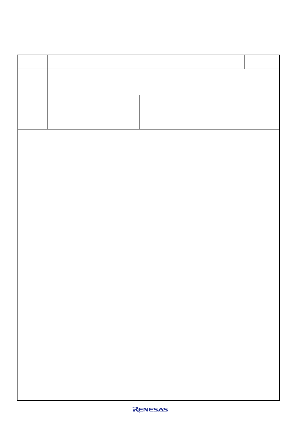
Product
Category
Resolver-to-digital converter ICs
Document
No.
Rev.
1.00
Title
Correction of errors and addition of a control
register
Information
Category
Technical Notification
Applicable
Product
RAA3064002GFP
RAA3064003GFP
Lot No.
Reference
Document
Resolver-to-Digital Converters
User’s Manual: Hardware Rev.1.10
(r03uz0002ej0110)
All
TN-RDC-A0002A/E
This document is to notify you of the correction of errors and addition of a control register in the user’s manual of the
applicable products. The corrections were made in section 3.2.7, ALARM# Output Setting Register (ALMOUT) and section
3.2.12, Correction Circuit Gain Selection Register (CCGSL). Additions were made to table 3.1, List of Registers, and to section
3, Control Registers, as section 3.2.14, Over-Temperature Detection Circuit Control Register (FOPER).
(c) 2021. Renesas Electronics Corporation. All rights reserved. Page 1 of 6
Page 2
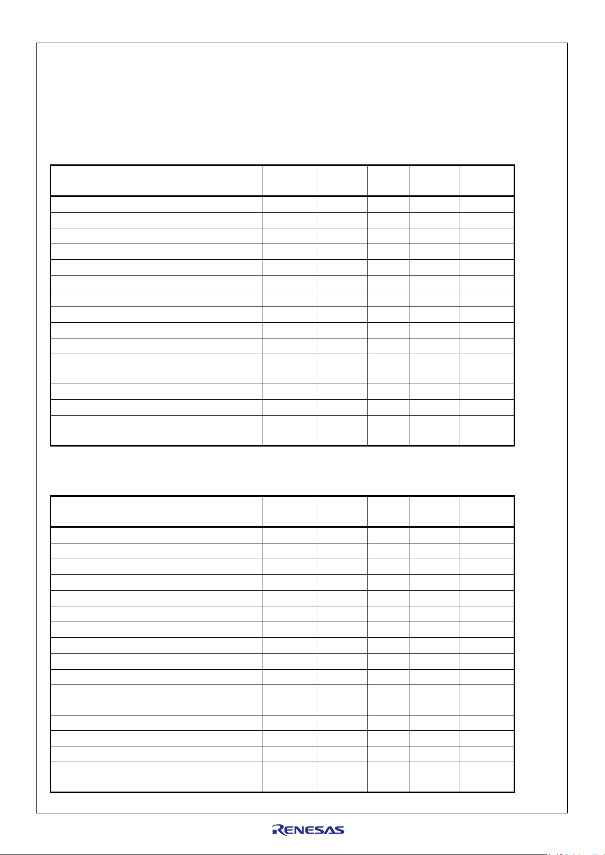
RENESAS TECHNICAL UPDATE TN-RDC-A0002A/E Date: Mar, 30, 2021
Register Name
Symbol
Number of
Bits
R/W
Address
Value After
a Reset
Power-saving control register 1
PS1 8 R/W
02H
00H
Power-saving control register 2
PS2 8 R/W
04H
00H
Power-saving control register 3
PS3 8 R/W
0AH
00H
Software reset register
SWRST
8
R/W
06H
00H
Differential amplifier input range monitoring register
DDMNT 8 R
0EH
00H
Alarm state register
ALMST
8
R/W
12H
FFH
ALARM# output setting register
ALMOUT
8
R/W
16H
00H
Monitor output selection register
MNTSL
8
R/W
20H
00H
Monitor output mode selection register
MDCACSEL
8
R/W
28H
00H
Differential amplification circuit gain selection register
GCGSL
8
R/W
2EH
00H
Phase adjustment circuit gain adjustment value
selection register
DLCGSL
8
R/W
30H
00H
Correction circuit gain selection register
CCGSL
8
R/W
36H
00H
Shunt current amplification circuit control register
CSACTL
8
R/W
42H
00H
Differential amplifier input level detection resetting
register
INITERR
8
R/W
54H
00H
Register Name
Symbol
Number of
Bits
R/W
Address
Value After
a Reset
Power-saving control register 1
PS1 8 R/W
02H
00H
Power-saving control register 2
PS2 8 R/W
04H
00H
Power-saving control register 3
PS3 8 R/W
0AH
00H
Software reset register
SWRST
8
R/W
06H
00H
Differential amplifier input range monitoring register
DDMNT 8 R
0EH
00H
Alarm state register
ALMST
8
R/W
12H
FFH
ALARM# output setting register
ALMOUT
8
R/W
16H
00H
Monitor output selection register
MNTSL
8
R/W
20H
00H
Monitor output mode selection register
MDCACSEL
8
R/W
28H
00H
Differential amplification circuit gain selection register
GCGSL
8
R/W
2EH
00H
Phase adjustment circuit gain adjustment value
selection register
DLCGSL
8
R/W
30H
00H
Correction circuit gain selection register
CCGSL
8
R/W
36H
00H
Shunt current amplification circuit control register
CSACTL
8
R/W
42H
00H
Over-temperature detection circuit control register
FOPER
8
R/W
48H
00H
Differential amplifier input level detection resetting
register
INITERR
8
R/W
54H
00H
Page 18 of 52
A control register was added to table 3.1, List of Registers, as follows.
[Before Addition]
3.1 List of Registers
Table 3.1 List of Registers
[After Addition]
Table 3.1 List of Registers
Page 2 of 6
Page 3
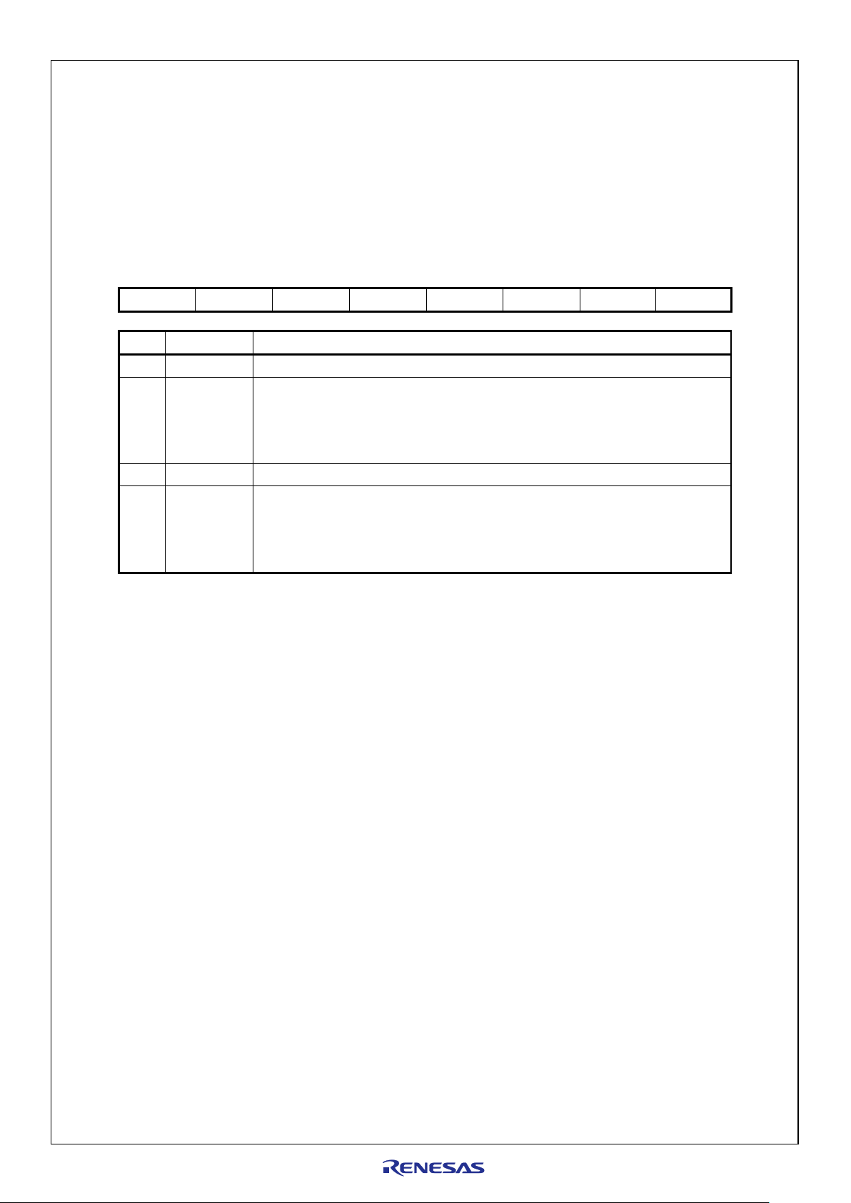
Address: 16H Value after a reset: 00H R/W: R/W
7 6 5 4 3 2 1
0
0 0 0
DDAN 0 0 0 TSDAN
Bit
Bit Name
Function
7 to 5
⎯
Reserved
4
DDAN
0: The active level of the ALAMR# signal is not output on detection of the input signals to a
differential amplifier being out of the V
INX
range.
1: The active level of the ALAMR# signal is output on detection of the input signals to a
differential amplifier being within the V
INX
range.
3 to 1
⎯
Reserved
0
TSDAN
0: The active level of the ALARM# signal is not output on detection of an excessive
temperature (125°C or above).
1: The active level of the ALARM# signal is output on detection of an excessive temperature
(125°C or above).
RENESAS TECHNICAL UPDATE TN-RDC-A0002A/E Date: Mar, 30, 2021
Page 24 of 52
Section 3.2.7, ALARM# Output Setting Register (ALMOUT), was corrected as follows.
[Before Correction]
3.2.7 ALARM# Output Setting Register (ALMOUT)
The ALMOUT register is used to specify the source of the ALARM# output.
Remark Bits 7 to 5 and 3 to 1 are read as 0. The write value should also be 0.
When the DDAN and TSDAN bits are set to 1, the reason for the output of the active level of ALARM# can be checked by
reading the ALMST register (see Differential Amplifier Input Range Monitoring Register (DDMNT)).
Page 3 of 6
Page 4

Address: 16H Value after a reset: 00H R/W: R/W
7 6 5 4 3 2 1
0
0 0 0
DDAN 0 0 0 TSDAN
Bit
Bit Name
Function
7 to 5
⎯
Reserved
4
DDAN
0: The active level of the ALAMR# signal is not output on detection of the input signals to a
differential amplifier being out of the V
INX
range.
1: The active level of the ALAMR# signal is output on detection of the input signals to a
differential amplifier being within the V
INX
range.
3 to 1
⎯
Reserved
0
TSDAN
0: The active level of the ALARM# signal is not output on detection of an excessive
temperature (125°C or above).
1: The active level of the ALARM# signal is output on detection of an excessive temperature
(125°C or above).
RENESAS TECHNICAL UPDATE TN-RDC-A0002A/E Date: Mar, 30, 2021
[After Correction]
3.2.7 ALARM# Output Setting Register (ALMOUT)
The ALMOUT register is used to specify the source of the ALARM# output.
Remark Bits 7 to 5 and 3 to 1 are read as 0. The write value should also be 0.
To enable over-temperature detection, write 1 to the TSDAN bit in this register and to the TSDEN bit in the FOPER register.
When the DDAN and TSDAN bits are set to 1, the reason for the output of the active level of ALARM# can be checked by
reading the ALMST register (see Differential Amplifier Input Range Monitoring Register (DDMNT)).
Page 4 of 6
Page 5
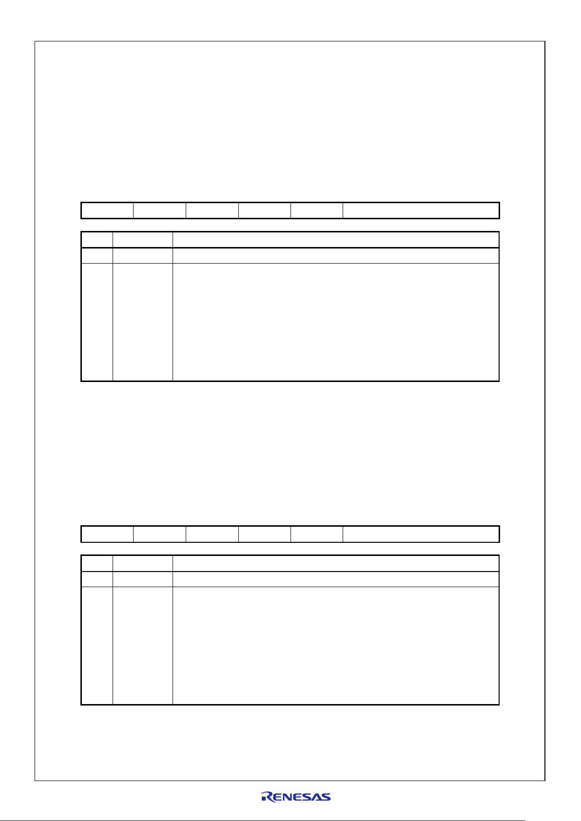
Address: 36H Value after a reset: 00H R/W: R/W
7 6 5 4 3 2 1
0
0 0 0 0 0
CCG[2:0]
Bit
Bit Name
Function
7 to 3
⎯
Reserved
2 to 0
CCG[2:0]
Select the gain of the correction circuit
000: 2/25
001: 4/25
010: 8/25
011: 1/100
100: 2/100
101: 4/100
Others: Setting prohibited
Address: 36H Value after a reset: 00H R/W: R/W
7 6 5 4 3 2 1
0
0 0 0 0 0
CCG[2:0]
Bit
Bit Name
Function
7 to 3
⎯
Reserved
2 to 0
CCG[2:0]
Select the gain of the correction circuit
000: 1/100
001: 2/100
010: 4/100
011: 2/25
100: 4/25
101: 8/25
Others: Setting prohibited
RENESAS TECHNICAL UPDATE TN-RDC-A0002A/E Date: Mar, 30, 2021
Page 27 of 52
Section 3.2.12, Correction Circuit Gain Selection Register (CCGSL), was corrected as follows.
[Begore Correction]
3.2.12 Correction Circuit Gain Selection Register (CCGSL)
The CCGSL register is used to select the gain of the correction circuit.
Remark Bits 7 to 3 are read as 0. The write value should also be 0.
[After Correction]
3.2.12 Correction Circuit Gain Selection Register (CCGSL)
The CCGSL register is used to select the gain of the correction circuit.
Remark Bits 7 to 3 are read as 0. The write value should also be 0.
Page 5 of 6
Page 6

Address: 48H Value after a reset: 00H R/W: R/W
7 6 5 4 3 2 1
0
0 0 0 0 0 0 0
TSDEN
Bit
Bit Name
Function
7 to 1
⎯
Reserved
0
TSDEN
Control of the thermal comparator circuit
0: Stops operation.
1: Starts operation.
RENESAS TECHNICAL UPDATE TN-RDC-A0002A/E Date: Mar, 30, 2021
Page 29 of 52
Section 3.2.14, Over-Temperature Detection Circuit Control Register (FOPER), was added.
[Addition]
3.2.14 Over-Temperature Detection Circuit Control Register (FOPER)
The FOPER register is used to control of the thermal comparator circuit.
Remark Bits 7 to 1 are read as 0. The write value should also be 0.
To enable over-temperature detection, write 1 to the TSDAN bit in the ALMOUT register and to the TSDEN bit in this register.
End of document
Page 6 of 6
 Loading...