

Page 1
Rev. 1.10 January 2021
Renesas RA Family
RA6 Series
RA6T1 Group
Motor Control Evaluation System for RA Family
- RA6T1 Group
User’s Manual
User’ s Manua
l
All information contained in these materials, including products and product specifications,
represents information on the product at the time of publication and is subject to change by
Renesas Electronics Corp. without notice. Please review the latest information published by
Renesas Electronics Corp. through various means, including the Renesas Electronics Corp.
website (http://www.renesas.com).
www.renesas.com
Page 2

© 2020 Renesas Electronics Corporation. All rights reserved.
Notice
1. Descriptions of circuits, software and other related information in this document are provided only to illustrate the operation of semiconductor products
and application examples. You are fully responsible for the incorporation or any other use of the circuits, software, and information in the design of your
product or system. Renesas Electronics disclaims any and all liability for any losses and damages incurred by you or third parties arising from the use of
these circuits, software, or information.
2. Renesas Electronics hereby expressly disclaims any warranties against and liability for infringement or any other claims involving patents, copyrights, or
other intellectual property rights of third parties, by or arising from the use of Renesas Electronics products or technical information described in this
document, including but not limited to, the product data, drawings, charts, programs, algorithms, and application examples.
3. No license, express, implied or otherwise, is granted hereby under any patents, copyrights or other intellectual property rights of Renesas Electronics or
others.
4. You shall not alter, modify, copy, or reverse engineer any Renesas Electronics product, whether in whole or in part. Renesas Electronics disclaims any
and all liability for any losses or damages incurred by you or third parties arising from such alteration, modification, copying or reverse engineering.
5. Renesas Electronics products are classified according to the following two quality grades: “Standard” and “High Quality”. The intended applications for
each Renesas Electronics product depends on the product’s quality grade, as indicated below.
"Standard": Computers; office equipment; communications equipment; test and measurement equipment; audio and visual equipment; home
electronic appliances; machine tools; personal electronic equipment; industrial robots; etc.
"High Quality": Transportation equipment (automobiles, trains, ships, etc.); traffic control (traffic lights); large-scale communication equipment; key
financial terminal systems; safety control equipment; etc.
Unless expressly designated as a high reliability product or a product for harsh environments in a Renesas Electronics data sheet or other Renesas
Electronics document, Renesas Electronics products are not intended or authorized for use in products or systems that may pose a direct threat to
human life or bodily injury (artificial life support devices or systems; surgical implantations; etc.), or may cause serious property damage (space system;
undersea repeaters; nuclear power control systems; aircraft control systems; key plant systems; military equipment; etc.). Renesas Electronics disclaims
any and all liability for any damages or losses incurred by you or any third parties arising from the use of any Renesas Electronics product that is
inconsistent with any Renesas Electronics data sheet, user’s manual or other Renesas Electronics document.
6. When using Renesas Electronics products, refer to the latest product information (data sheets, user’s manuals, application notes, “General Notes for
Handling and Using Semiconductor Devices” in the reliability handbook, etc.), and ensure that usage conditions are within the ranges specified by
Renesas Electronics with respect to maximum ratings, operating power supply voltage range, heat dissipation characteristics, installation, etc. Renesas
Electronics disclaims any and all liability for any malfunctions, failure or accident arising out of the use of Renesas Electronics products outside of such
specified ranges.
7. Although Renesas Electronics endeavors to improve the quality and reliability of Renesas Electronics products, semiconductor products have specific
characteristics, such as the occurrence of failure at a certain rate and malfunctions under certain use conditions. Unless designated as a high reliability
product or a product for harsh environments in a Renesas Electronics data sheet or other Renesas Electronics document, Renesas Electronics products
are not subject to radiation resistance design. You are responsible for implementing safety measures to guard against the possibility of bodily injury,
injury or damage caused by fire, and/or danger to the public in the event of a failure or malfunction of Renesas Electronics products, such as safety
design for hardware and software, including but not limited to redundancy, fire control and malfunction prevention, appropriate treatment for aging
degradation or any other appropriate measures. Because the evaluation of microcomputer software alone is very difficult and impractical, you are
responsible for evaluating the safety of the final products or systems manufactured by you.
8. Please contact a Renesas Electronics sales office for details as to environmental matters such as the environmental compatibility of each Renesas
Electronics product. You are responsible for carefully and sufficiently investigating applicable laws and regulations that regulate the inclusion or use of
controlled substances, including without limitation, the EU RoHS Directive, and using Renesas Electronics products in compliance with all these
applicable laws and regulations. Renesas Electronics disclaims any and all liability for damages or losses occurring as a result of your noncompliance
with applicable laws and regulations.
9. Renesas Electronics products and technologies shall not be used for or incorporated into any products or systems whose manufacture, use, or sale is
prohibited under any applicable domestic or foreign laws or regulations. You shall comply with any applicable export control laws and regulations
promulgated and administered by the governments of any countries asserting jurisdiction over the parties or transactions.
10. It is the responsibility of the buyer or distributor of Renesas Electronics products, or any other party who distributes, disposes of, or otherwise sells or
transfers the product to a third party, to notify such third party in advance of the contents and conditions set forth in this document.
11. This document shall not be reprinted, reproduced or duplicated in any form, in whole or in part, without prior written consent of Renesas Electronics.
12. Please contact a Renesas Electronics sales office if you have any questions regarding the information contained in this document or Renesas
Electronics products.
(Note1) “Renesas Electronics” as used in this document means Renesas Electronics Corporation and also includes its directly or indirectly controlled
subsidiaries.
(Note2) “Renesas Electronics product(s)” means any product developed or manufactured by or for Renesas Electronics.
(Rev.4.0-1 November 2017)
Corporate Headquarters
Contact information
TOYOSU FORESIA, 3-2-24 Toyosu,
Koto-ku, Tokyo 135-0061, Japan
www.renesas.com
For further information on a product, technology, the most up-to-date
version of a document, or your nearest sales office, please visit:
www.renesas.com/contact/.
Trademarks
Renesas and the Renesas logo are trademarks of Renesas Electronics
Corporation. All trademarks and registered trademarks are the property
of their respective owners.
Page 3

© 2019 Renesas Electronics Corporation. All rights reserved.
General Precautions in the Handling of Microprocessing Unit and Microcontroller
Unit Products
The following usage notes are applicable to all Microprocessing unit and Microcontroller unit products from Renesas. For detailed usage notes on the products
covered by this document, refer to the relevant sections of the document as well as any technical updates that have been issued for the products.
1. Precaution against Electrostatic Discharge (ESD)
A strong electrical field, when exposed to a CMOS device, can cause destruction of the gate oxide and ultimately degrade the device operation. Steps
must be taken to stop the generation of static electricity as much as possible, and quickly dissipate it when it occurs. Environmental control must be
adequate. When it is dry, a humidifier should be used. This is recommended to avoid using insulators that can easily build up static electricity.
Semiconductor devices must be stored and transported in an anti-static container, static shielding bag or conductive material. All test and
measurement tools including work benches and floors must be grounded. The operator must also be grounded using a wrist strap. Semiconductor
devices must not be touched with bare hands. Similar precautions must be taken for printed circuit boards with mounted semiconductor devices.
2. Processing at power-on
The state of the product is undefined at the time when power is supplied. The states of internal circuits in the LSI are indeterminate and the states of
register settings and pins are undefined at the time when power is supplied. In a finished product where the reset signal is applied to the external reset
pin, the states of pins are not guaranteed from the time when power is supplied until the reset process is completed. In a similar way, the states of pins
in a product that is reset by an on-chip power-on reset function are not guaranteed from the time when power is supplied until the power reaches the
level at which resetting is specified.
3. Input of signal during power-off state
Do not input signals or an I/O pull-up power supply while the device is powered off. The current injection that results from input of such a signal or I/O
pull-up power supply may cause malfunction and the abnormal current that passes in the device at this time may cause degradation of internal
elements. Follow the guideline for input signal during power-off state as described in your product documentation.
4. Handling of unused pins
Handle unused pins in accordance with the directions given under handling of unused pins in the manual. The input pins of CMOS products are
generally in the high-impedance state. In operation with an unused pin in the open-circuit state, extra electromagnetic noise is induced in the vicinity of
the LSI, an associated shoot-through current flows internally, and malfunctions occur due to the false recognition of the pin state as an input signal
become possible.
5. Clock signals
After applying a reset, only release the reset line after the operating clock signal becomes stable. When switching the clock signal during program
execution, wait until the target clock signal is stabilized. When the clock signal is generated with an external resonator or from an external oscillator
during a reset, ensure that the reset line is only released after full stabilization of the clock signal. Additionally, when switching to a clock signal
produced with an external resonator or by an external oscillator while program execution is in progress, wait until the target clock signal is stable.
6. Voltage application waveform at input pin
Waveform distortion due to input noise or a reflected wave may cause malfunction. If the input of the CMOS device stays in the area between VIL
(Max.) and VIH (Min.) due to noise, for example, the device may malfunction. Take care to prevent chattering noise from entering the device when the
input level is fixed, and also in the transition period when the input level passes through the area between VIL (Max.) and VIH (Min.).
7. Prohibition of access to reserved addresses
Access to reserved addresses is prohibited. The reserved addresses are provided for possible future expansion of functions. Do not access these
addresses as the correct operation of the LSI is not guaranteed.
8. Differences between products
Before changing from one product to another, for example to a product with a different part number, confirm that the change will not lead to problems.
The characteristics of a microprocessing unit or microcontroller unit products in the same group but having a different part number might differ in terms
of internal memory capacity, layout pattern, and other factors, which can affect the ranges of electrical characteristics, such as characteristic values,
operating margins, immunity to noise, and amount of radiated noise. When changing to a product with a different part number, implement a systemevaluation test for the given product.
Page 4

User’s Manual
R12UZ0078EJ0110 Rev 1.10 Page 1 of 30
January 28, 2021
Renesas RA Family
Motor Control Evaluation System for RA Family - RA6T1
Group User’s Manual
Contents
1. Overview ................................................................................................................................. 4
1.1 Presupposition and precautions of this document .................................................................................. 6
2. Product Contents ..................................................................................................................... 7
3. Product Order Information ....................................................................................................... 7
4. Hardware Configuration and Default Setting ............................................................................ 8
4.1 Hardware configuration ........................................................................................................................... 8
4.2 Block diagram ........................................................................................................................................ 11
4.3 Jumper pin setting ................................................................................................................................. 12
5. Inverter Board Specification ................................................................................................... 13
5.1 Overview ................................................................................................................................................ 13
5.2 Functions ............................................................................................................................................... 13
5.2.1 Inverter control circuit block ................................................................................................................. 13
5.2.2 Current detection circuit ...................................................................................................................... 14
5.2.3 Overcurrent detection circuit ............................................................................................................... 15
5.2.4 Output voltage detection circuit ........................................................................................................... 16
5.2.5 Voltage generation circuit .................................................................................................................... 16
5.2.6 LED ...................................................................................................................................................... 17
5.2.7 Toggle switch and push switch ............................................................................................................ 17
5.2.8 Variable resistor................................................................................................................................... 17
5.3 Pin assignment ...................................................................................................................................... 18
5.3.1 Connector pin function assignment ..................................................................................................... 18
6. RA6T1 CPU Card Specification ............................................................................................. 20
6.1 Overview ................................................................................................................................................ 20
6.2 Functions ............................................................................................................................................... 20
6.2.1 Power supply ....................................................................................................................................... 20
6.2.2 Onboard emulator ............................................................................................................................... 20
6.2.3 Inverter board connector ..................................................................................................................... 21
6.2.4 Serial communication connector ......................................................................................................... 22
6.2.5 Hall sensor signal input ....................................................................................................................... 22
6.2.6 Encoder signal input ............................................................................................................................ 22
6.2.7 Unused pins ......................................................................................................................................... 23
Page 5

Renesas RA Family Motor Control Evaluation System for RA Family - RA6T1 Group
User's Manual
R12UZ0078EJ0110 Rev 1.10 Page 2 of 30
January 28, 2021
6.2.8 Reset circuit ......................................................................................................................................... 23
6.2.9 LED ...................................................................................................................................................... 23
6.2.10 CAN Communication ........................................................................................................................... 23
6.2.11 SPI communication ............................................................................................................................. 24
6.2.12 2nd inverter board connection ............................................................................................................. 24
6.2.13 RA6T1 pin function list ........................................................................................................................ 25
7. Certification ........................................................................................................................... 28
7.1 European Union regulatory notices ....................................................................................................... 28
8. Design and Manufacture Information ..................................................................................... 29
9. Website and Support ............................................................................................................. 29
Figure of contents
Figure 1-1 Main board (top view) ...................................................................................................................... 5
Figure 1-2 Main board (bottom view) ................................................................................................................. 5
Figure 2-1 Product contents .............................................................................................................................. 7
Figure 4-1 Motor Control Evaluation System for RA Family - RA6T1 Group .................................................. 11
Figure 4-2 Jumper pin setting .......................................................................................................................... 12
Figure 5-1 Illustration of inverter control circuit block ...................................................................................... 13
Figure 5-2 Current detection circuit ................................................................................................................. 14
Figure 5-3 Overcurrent detection circuit .......................................................................................................... 15
Figure 5-4 Output voltage detection circuit ...................................................................................................... 16
Page 6

Renesas RA Family Motor Control Evaluation System for RA Family - RA6T1 Group
User's Manual
R12UZ0078EJ0110 Rev 1.10 Page 3 of 30
January 28, 2021
Table of contents
Table 4-1 Motor Control Evaluation System for RA Family - RA6T1 Group specification (1/3) ........................ 8
Table 4-2 Motor Control Evaluation System for RA Family - RA6T1 Group specification (2/3) ........................ 9
Table 4-3 Motor Control Evaluation System for RA Family - RA6T1 Group specification (3/3) ...................... 10
Table 4-4 Jumper pin setting ........................................................................................................................... 12
Table 5-1 Relation between Iin and Vout ........................................................................................................ 14
Table 5-2 Voltage generation circuit ................................................................................................................ 16
Table 5-3 LED .................................................................................................................................................. 17
Table 5-4 Toggle switch and push switch........................................................................................................ 17
Table 5-5 Variable resistance specification ..................................................................................................... 17
Table 5-6 Board-to Board connector (CNA) .................................................................................................... 18
Table 5-7 Board-to Board connector (CNB) .................................................................................................... 19
Table 5-8 Board-to-Board connector (CN10) .................................................................................................. 19
Table 6-1 Inverter board connector (CNA) pin assignment ............................................................................. 21
Table 6-2 Inverter board connector (CNB) pin assignment ............................................................................. 21
Table 6-3 Serial communication connector (CN10) pin assignment ............................................................... 22
Table 6-4 Pin for hall sensor signal input (CN5) pin assignment .................................................................... 22
Table 6-5 Through holes for encoder signal input (CN7) pin assignment ....................................................... 22
Table 6-6 Through hole for unused pin (CN9) pin assignment ....................................................................... 23
Table 6-7 LED pin assignment ........................................................................................................................ 23
Table 6-8 CAN communication pin assignment .............................................................................................. 23
Table 6-9 SPI communication pin assignment ................................................................................................ 24
Table 6-10 2nd inverter board connector (CNC) pin assignment .................................................................... 24
Table 6-11 RA6T1 pin function list .................................................................................................................. 25
Page 7

Renesas RA Family Motor Control Evaluation System for RA Family - RA6T1 Group
User's Manual
R12UZ0078EJ0110 Rev 1.10 Page 4 of 30
January 28, 2021
1. Overview
Motor Control Evaluation System for RA Family - RA6T1 Group is a motor control evaluation kit. By using
this product, motor control can be performed easily.
Motor Control Evaluation System for RA Family - RA6T1 Group has characteristics shown below.
(1) Supports permanent magnet synchronous motor.
(2) Supports 3-shunt current detection.
(3) Equipped with USB mini B for Motor Control Development Support Tool communication.
(4) Provides overcurrent protection function using overcurrent detection circuit.
Motor Control Evaluation System for RA Family - RA6T1 Group consists of 2 boards, which are the inverter
board and the RA6T1 CPU Card. Main functions are listed below.
① Inverter board
・ Operating input voltage : DC24~48V
⁻ DC jack (J1)
⁻ Power supply connector (CN1)
・ Switch
⁻ Toggle switch (SW1)
⁻ Push switch (SW2)
・ LED
⁻ LED1, LED2, LED3
⁻ LED for power source for inverter control circuit block
・ Connector
⁻ Board to board connector (CNA, CNB)
⁻ USB minB connector
⁻ Motor connector (CN2)
・ Variable resistor (VR1)
② RA6T1 CPU Card
・ R7FA6T1AD3CFP MCU (hereinafter called “RA MCU”)
・ Connector
⁻ Board to board connector (CNA, CNB)
⁻ USB connector for J-Link OB
⁻ SCI connector for Renesas Motor Workbench communication
⁻ Through hole for CAN communication
⁻ Through hole for SPI communication
⁻ Connector for hall sensor signal input
⁻ Connector for encoder signal input
⁻ 10/20 pin through hole for Arm debugger
⁻ Through hole for 2nd inverter
⁻ Connection pattern for J-Link 6pin Needle Adapter
・ LED
LED for user control x2
・ Switch
Switch for MCU external reset
Page 8
Renesas RA Family Motor Control Evaluation System for RA Family - RA6T1 Group
User's Manual
R12UZ0078EJ0110 Rev 1.10 Page 5 of 30
January 28, 2021
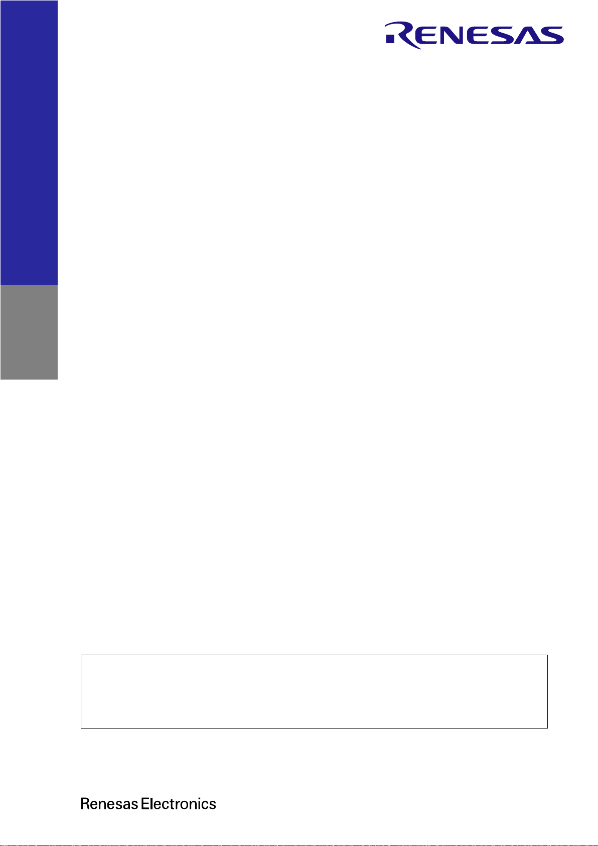
Through hole for
CAN communication
SCI connector
for RMW
communication
Hall signal
input connector
USB connector for
J-Link OB
Through hole for
2nd inverter
Through hole for
SPI communication
Encoder signal
Input connector
Motor connector
DC jack
Power supply
terminal block
switch
LED
Renesas Motor
Workbench
Communication
circuit connector
Variable resistor
Figure 1-1 Main board (top view)
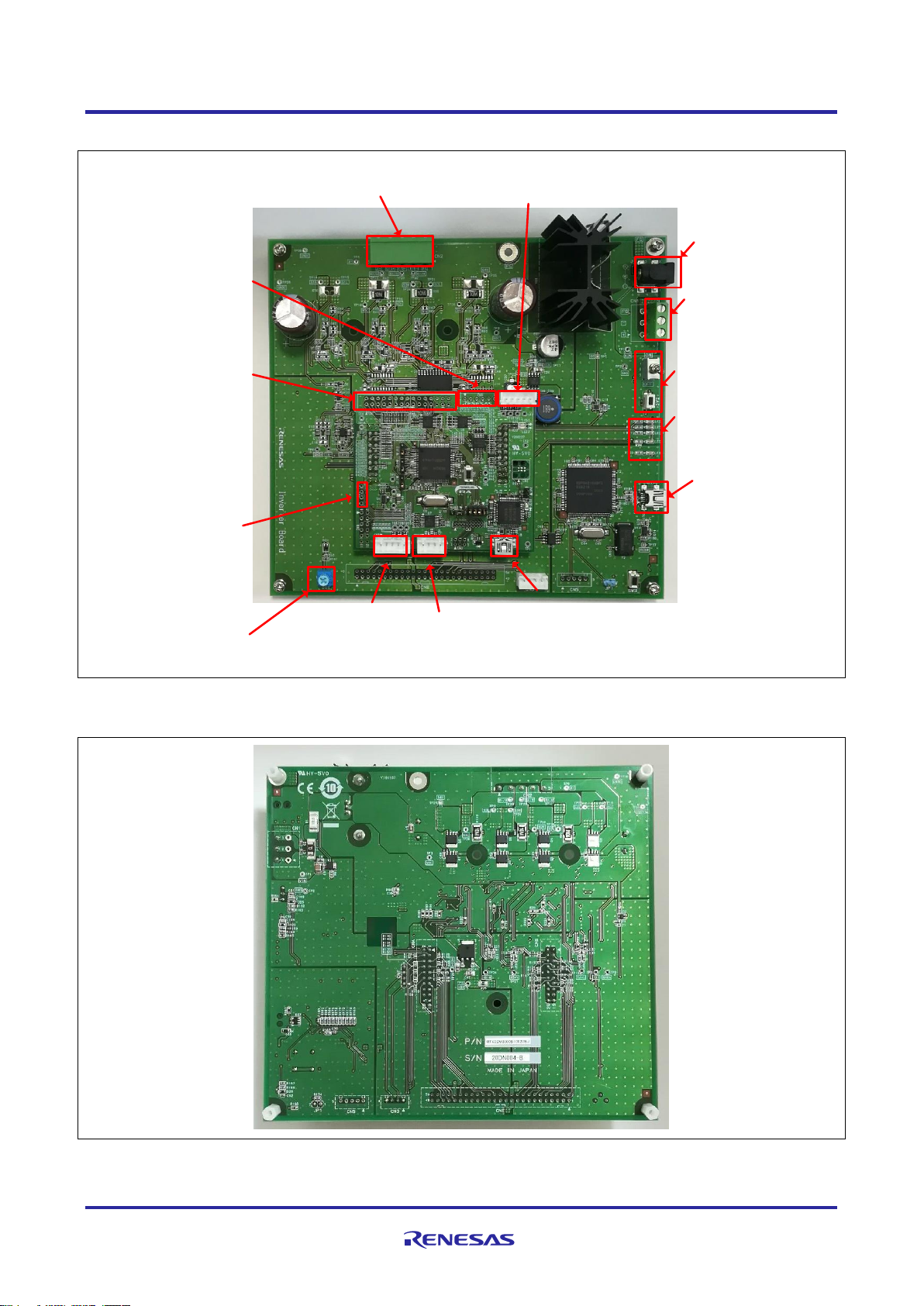
Figure 1-2 Main board (bottom view)
Page 9

Renesas RA Family Motor Control Evaluation System for RA Family - RA6T1 Group
User's Manual
R12UZ0078EJ0110 Rev 1.10 Page 6 of 30
January 28, 2021
1.1 Presupposition and precautions of this document
1. Experience of using tools: This document assumes that the user has used terminal emulation program of
Integrated Development Environment (IDE) such as e2 studio before.
2. Knowledge about the development subject: This document assumes that the user has a basic knowledge
to modify the sample project regarding MCU and embedded system.
3. Before using this product, wear an antistatic wrist strap. If you touch this product with static charge on
your body, a device failure may occur or operation may become unstable
4. To use this product prepare the following items, too.
・Stabilized power supply : Output voltage of DC24 V or higher, the upper limit of the output current
can be set at 1A
・Power supply cable (x2) :Cables which enable to apply the current of 1A or higher.
(To connect the stabilized power supply and the inverter board)
5. All screen shots provided in this document is for reference. Actual screen displays may differ depending
on the software and development tool version which you use.
Page 10
Renesas RA Family Motor Control Evaluation System for RA Family - RA6T1 Group
User's Manual
R12UZ0078EJ0110 Rev 1.10 Page 7 of 30
January 28, 2021
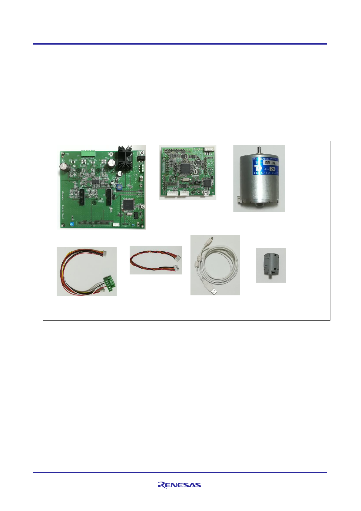
2. Product Contents
This kit consists of the following parts.
1. Inverter Board (RTK0EM0000B10020BJ)
2. RA6T1 CPU Card (RTK0EMA170C00000BJ)
3. Brushless DC Mortor (TG-55L-KA 24V)
4. Motor Cable
5. Communication Cable
6. USB Cable
7. Ferrite Core
(1)Inverter board
(2)RA6T1 CPU card
(3)Brushless DC motor
(4)Motor cable
(5)communication cable
(6)USB cable
(7)Ferrite core
Figure 2-1 Product contents
3. Product Order Information
Product model name to order Motor Control Evaluation System for RA Family - RA6T1 Group:
RTK0EMA170S00020BJ
Page 11
Renesas RA Family Motor Control Evaluation System for RA Family - RA6T1 Group
User's Manual
R12UZ0078EJ0110 Rev 1.10 Page 8 of 30
January 28, 2021
4. Hardware Configuration and Default Setting
4.1 Hardware configuration
Motor Control Evaluation System for RA Family - RA6T1 Group consists of the inverter board and the RA6T1
CPU Card. Specifications as a kit and for the relevant boards are listed below.
Table 4-1 Motor Control Evaluation System for RA Family - RA6T1 Group specification (1/3)
Item
Specification
Product name
Motor Control Evaluation System for RA Family - RA6T1 Group
Kit model name
RTK0EMA170S00020BJ
Kit configuration
Inverter board
RTK0EM0000B10020BJ
RA6T1 CPU Card
RTK0EMA170C00000BJ
Permanent Magnet Synchronous Motor
TG-55L-KA (Tsukasa Electric Co.,LTD)
Rated voltage:24[V]
Rated current:0.42[A]
Inverter circuit‐
CPU card
Non-isolated
External view
Note: The actual product may differ from this photo.
Board size
Inverter board:175 mm (width) x 160 mm (length)
RAT1 CPU Card :78 mm (width) x 70 mm (length)
Operating temperature
Room temperature
Operating humidity
No condensation allowed
EMC Directive
Europe:EN61326-1 : 2013 Class A
Page 12

Renesas RA Family Motor Control Evaluation System for RA Family - RA6T1 Group
User's Manual
R12UZ0078EJ0110 Rev 1.10 Page 9 of 30
January 28, 2021
Table 4-2 Motor Control Evaluation System for RA Family - RA6T1 Group specification (2/3)
Item
Specification
Product name
Inverter board
Board model name
RTK0EM0000B10020BJ
External view
Note: The actual product may differ from this photo.
Operating input voltage
DC 24~48 V (±5%)
Select one from the below
Power supply connector
Center-positive DC jack
Maximum input power
250 W
Rated output capacity
250 VA
Rated output current
AC 5 A (RMS value)
Switching frequency
2 kHz ~ 20 kHz (Reference value)
Current detection method
3-shunt method
Shunt resistor
10 mohm
PWM logic
Lower arm: Positive logic Upper arm: Negative logic
DC bus voltage detection
(bus voltage detection)
Detection by resistance division (5 V ~ 48 V)
3-phase output voltage
detection
Detection by resistance division (0 V ~ 48 V)
3-phase output current
detection
MOSFET Detection using shunt resistor under the source (-10 A ~ +10 A)
Overcurrent detection
function
10 A
Communication interface
USB mini B
*Communicating with PC requires Motor Control Development Support Tool by
Renesas Electronics.
Connector
・ CPU card connector x2
・ USB mini B connector
・ Power input connector
・ Motor connector
Switch
・ Toggle switch x1
・ Push switch x1
LED
・ LED x3
・ LED for power source for inverter control circuit block
Page 13

Renesas RA Family Motor Control Evaluation System for RA Family - RA6T1 Group
User's Manual
R12UZ0078EJ0110 Rev 1.10 Page 10 of 30
January 28, 2021
Table 4-3 Motor Control Evaluation System for RA Family - RA6T1 Group specification (3/3)
item
Specification
Product name
RA6T1 CPU Card
Board model name
RTK0EMA170C00000BJ
Compatible inverter board / product
name
Inverter board supplied with Evaluation System for BLDC Motor /
RTK0EM0000B10020BJ
External view
Note: The actual product may differ from this photo.
Mounted MCU
Product group
RA6T1 group
Product name
R7FA6T1AD3CFP
CPU maximum
operating frequency
120MHz
Bit number
32 bit
Package / Pin number
LFQFP / 100 pin
RAM
512K byte
MCU input clock
10MHz (Generate with external crystal oscillator)
Input power supply voltage
DC 5V (±5%)
Select one from the below
Power is supplied from compatible inverter board
Power is supplied from USB connector
Compatible sensor
Hall sensor、Encoder
Compatible emulator
J-Link-OB (Onboard emulator circuit)
Connector
Inverter board connector x2
USB connector for J-Link OB
SCI connector for Renesas Motor Workbench communication
Through hole for CAN communication
Through hole for SPI communication
Connector for hall sensor signal input
Connector for encoder signal input
10/20 pin through hole for Arm debugger
Through hole for 2nd inverter
Connection pattern for J-Link 6pin Needle Adapter
Switch
Switch for MCU external reset
LED
LED for user control x2
Operating temperature
Room temperature
Operating humid
No condensation allowed
Page 14

Renesas RA Family Motor Control Evaluation System for RA Family - RA6T1 Group
User's Manual
R12UZ0078EJ0110 Rev 1.10 Page 11 of 30
January 28, 2021
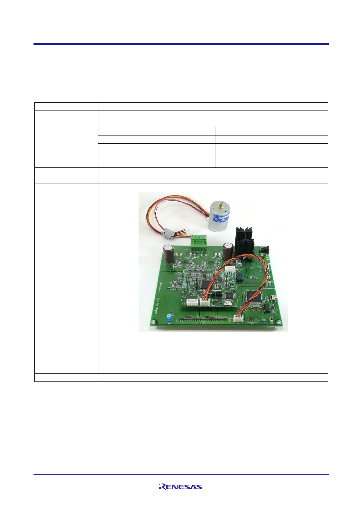
4.2 Block diagram
Power
Supply
Connector
Volume
Toggle Switch
/Push Switch
12V Voltage
Generation
Function
Overcurrent
detection
5V Voltage
Generation
Function
Inverter Circuit
Gate Driver
Motor
Connector
Board to
board
connector
24-48V
12V
Overcurrent detection
3 phase complementary PWM
5V
MCU
RA6T1
Through hole for 2nd
inverter
USB
Connector
Crystal
Oscillator
Reset
switch
LED * 3
Output Voltage
Division
J-Link On
Board
Motor development support tool
Renesas Motor Workbench Communication circuit
USB
Connector
Digital
Isolator
Current
Detection
Amplifier
LED * 2
Inverter Board
Hall Sensor
Connector
Encoder Connector
CAN Communication
Connector
SPI Communication
Connector
CPU Card
Shunt Resistor
MOSFETs
BLDC motor
SCI
Connector
SCI
Connector
Level
Shifter
Level
Shifter
Level
Shifter
Figure 4-1 Motor Control Evaluation System for RA Family - RA6T1 Group
Page 15
Renesas RA Family Motor Control Evaluation System for RA Family - RA6T1 Group
User's Manual
R12UZ0078EJ0110 Rev 1.10 Page 12 of 30
January 28, 2021
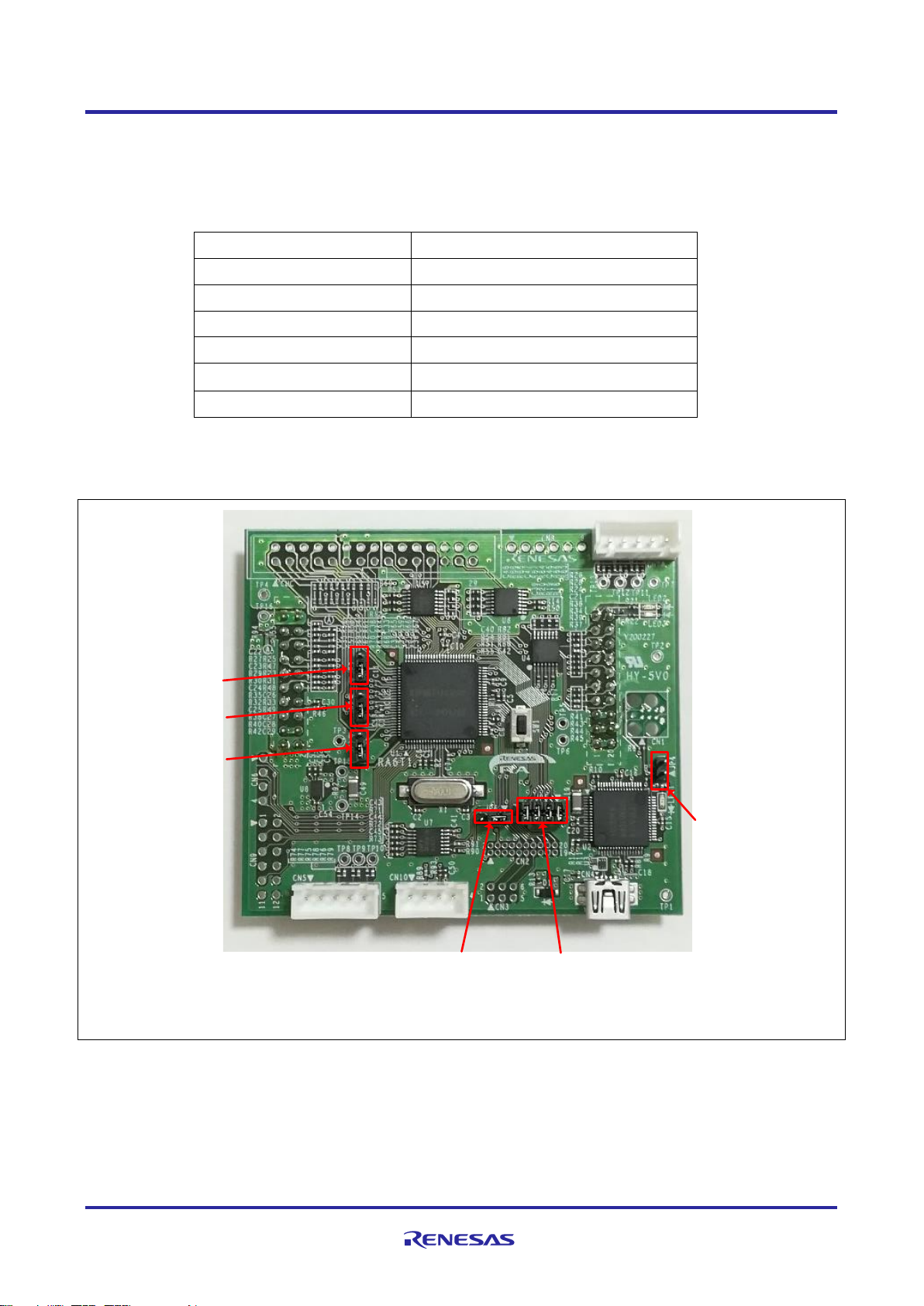
4.3 Jumper pin setting
Check that the jumper pins (JP1~JP6) are set as shown in the below table.
Table 4-4 Jumper pin setting
Jumper Pin
State
JP1
2-3pin short
JP2
2-3pin short
JP3
1-2pin short
JP4
1-2pin open
JP5
1-2pin, 3-4pin, 5-6pin, 7-8pin short
JP6
1-2pin short
A/D pins are via voltage dividers and offsets and so on. Refer to the circuit diagram for details.
JP3
1-2pin Short
JP2
2-3pin Short
JP1
2-3pin Short
JP4
1-2pin Open
JP5
1-2pin,3-4pin
5-6pin,7-8pin
Short
JP6
1-2pin Short
Figure 4-2 Jumper pin setting
Page 16
Renesas RA Family Motor Control Evaluation System for RA Family - RA6T1 Group
User's Manual
R12UZ0078EJ0110 Rev 1.10 Page 13 of 30
January 28, 2021
5. Inverter Board Specification
This section describes inverter board specification.
5.1 Overview
By connecting the inverter board with the CPU card by Renesas Electronics, motor can be operated.
5.2 Functions
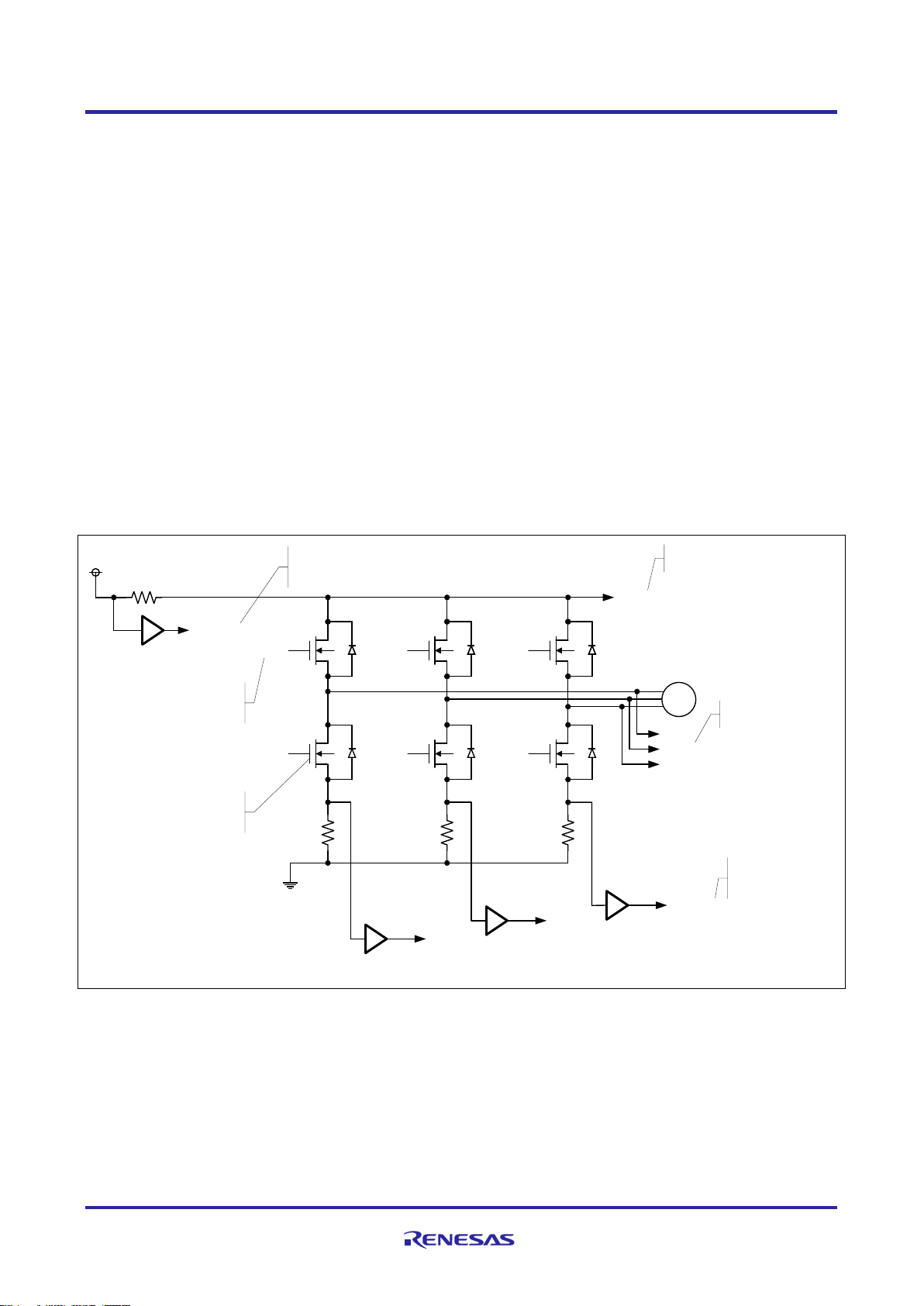
5.2.1 Inverter control circuit block
The INV-BRD has the inverter control circuit block which controls the motor with 6 POWER MOS-FETs.
POWER MOS-FET controls with 6-phase timer output by the microcontroller.
The inverter control circuit block outputs DC bus voltage, U, V and W phase voltage and shunt current to the
connectors (CNA, CNB). By entering these output values in A/D of the microcomputer of the CPU card,
analog values of the voltage and the shunt current of each phase can be measured. Refer to 5.2.2 and 5.2.4
for the current detection and the voltage detection, respectively. Also function to detect overcurrent from the
input current is available. Refer to 5.2.3 for details.
An illustration of the inverter control circuit block is shown in Figure 5-1. In the actual circuit, some inputs on
the A/D pins are via voltage dividers and offsets and so on. Refer to the circuit diagram for details.
Motor
UP
UN
VP
VN
WP
WN
V
BUS
CSA_U
CSA_V
CSA_W
AD_U
AD_V
AD_W
OP-Amp
OP-Amp
OP-Amp
HISIDE_OC
Motor Control
PWM Input
DC Bus Voltage
Phase Voltages
Shunt Current
(via Amplifier)
POWER
MOS- FET
Overcurrent
Detection
Figure 5-1 Illustration of inverter control circuit block
Page 17

Renesas RA Family Motor Control Evaluation System for RA Family - RA6T1 Group
User's Manual
R12UZ0078EJ0110 Rev 1.10 Page 14 of 30
January 28, 2021
5.2.2 Current detection circuit
The UNV-BRD has the current detection circuit to measure the current at the U, V and W phase. The current
detection circuit uses shunt resistance at each phase. Voltage drop caused by the current flowing through
the shunt resistor is amplified by the current detection amplifier to output. The relation between Iin which is
the current flowing through the shunt resistor and Vout which is the voltage output from the current detection
circuit is described by the below equation (1).
Vout[V] = Iin[A] × Rs[Ω] × 20 + 2.5 (1)
-
+
Iin
Vout
CSA_U
Rs
Rs : Shunt Resistor(0.01Ω)
Iin : Current Flow through Shunt Resistor
Vout : Voltage Applied to Connection Pin of CPU Card
CSA_V
CSA_W
-IN
+IN
+5V_A
VS
GND
AD8418A
Gain 20x
Figure 5-2 Current detection circuit
Table 5-1 Relation between Iin and Vout
Iin [A]
Vout[V]
10
4.5 2 2.9
0
2.5
-2
2.1
-10
0.5
Page 18

Renesas RA Family Motor Control Evaluation System for RA Family - RA6T1 Group
User's Manual
R12UZ0078EJ0110 Rev 1.10 Page 15 of 30
January 28, 2021
5.2.3 Overcurrent detection circuit
Detect the overcurrent from the input current, using the overcurrent detection circuit illustrated in Figure 5-3.
If the current value is within the range of threshold, detected overcurrent will be Low, although HISIDE_OC is
High. Therefore, by monitoring the OC pin and forcing the timer output pin into the Hi-Z state when OC is
low, you can protect the board and motor.
The overcurrent detection circuit does not directly protect the board and motor. Protect them by performing
appropriate processing with equipment such as microcontroller.
-
+
+IN
-IN
-
+
+5V_D
VIN
HISIDE_OC
Current Detection Signal
Comparator
Differential amplifier
Figure 5-3 Overcurrent detection circuit
Page 19

Renesas RA Family Motor Control Evaluation System for RA Family - RA6T1 Group
User's Manual
R12UZ0078EJ0110 Rev 1.10 Page 16 of 30
January 28, 2021
5.2.4 Output voltage detection circuit
The INV-BRD has the circuit that inputs bus voltage and three-phase output voltage (U, V and W phase) into
the AD pin of the microcontroller through resistive voltage divider. Relation between the three-phase output
voltage, the bus voltage and the detection voltage is described by the below equation (2).
Vout[𝑉]=
470
10 × 103+ 470
× 𝑉𝑖𝑛[𝑉
]
(2)
10k W
470 W
0.1mF
V
U
Vin Vout
V
V
V
W
V
BUS
Figure 5-4 Output voltage detection circuit
5.2.5 Voltage generation circuit
The INV- BRD generates voltage of 12V and 5V from the main power supply (24~48V)
Table 5-2 Voltage generation circuit
Item
Input voltage
[V]
Output voltage
(TYP.)[V]
Output current
(Max)[A]
Application
12Vgeneration
24~48
12
0.6
⚫ 5V generation
⚫ Gate driver IC
5Vgeneration
12 5 0.5
⚫ MCU power supply
Page 20

Renesas RA Family Motor Control Evaluation System for RA Family - RA6T1 Group
User's Manual
R12UZ0078EJ0110 Rev 1.10 Page 17 of 30
January 28, 2021
5.2.6 LED
The INV-BRD has three LEDs which the user can control. The user can control them from the RA6T1 CPU
Card.
Table 5-3 LED
Pins Compatible with CPU Card
Connector
LED1
LED2
LED3
CNA-1
Hi
Off ‐ ‐
Low
On
‐
‐
CNA-2
Hi
‐
Off ‐ Low
‐
On
‐
CNA-3
Hi
‐ ‐ Off
Low
‐
‐
On
5.2.7 Toggle switch and push switch
The INV-BRD has toggle switch (SW1) and push switch (SW2). The user can use them at his or her
discretion
Table 5-4 Toggle switch and push switch
Pins Compatible with CPU Card
Connector
SW1
SW2
CNA-13
Hi
OFF
‐
Low
ON
‐
CNA-14
Hi
‐
RELEASE
Low
‐
PUSH
5.2.8 Variable resistor
The INV-BRD has a variable resistor (VR1). The user can use the resistor at his or her discretion. If turning
the variable resistor clockwise, terminal voltage of the variable resistor (CNB-15) becomes low. If turning it
counterclockwise, the voltage becomes high
Table 5-5 Variable resistance specification
Item
Specification
Input voltage range
0~+5V_A
Variable resistor range
0~10k W
Page 21

Renesas RA Family Motor Control Evaluation System for RA Family - RA6T1 Group
User's Manual
R12UZ0078EJ0110 Rev 1.10 Page 18 of 30
January 28, 2021
5.3 Pin assignment
5.3.1 Connector pin function assignment
Table 5-6 Board-to Board connector (CNA)
Pin No.
Output
direction
Signal
Connection destination
(Inverter board)
Connection destination
(CPU card)
1
To INV
LED1#
LED1
U1.24 P408
2
To INV
LED2#
LED2
U1.25 P407
3
To INV
LED3#
LED3
U1.30 P207
4
To INV
VRL
-
Buffer output U4.6
5
To CPU
Overcurrent
detection
Comparator output U2.1
Buffer input U4.9
6
-
-
7
To INV
PWM phase WN
Gate driver U6.11 CLI
U1.55 P112/GTIOC3B
8
To INV
PWM phase VN
Gate driver U6.4 ALI
U1.57 P114/GTIOC2B
9
To INV
PWM phase UN
Gate driver U6.3 BLI
U1.18 P414/GTIOC0B
10
To INV
PWM phase WP
Gate driver U6 12 CHI
U1.54 P111/GTIOC3A
11
To INV
PWM phase VP
Gate driver U6.5 AHI
U1.56 P113/GTIOC2A
12
To INV
PWM phase UP
Gate driver U6.2 BHI
U1.17 P415/GTIOC0A
13
To CPU
SW1
SW1
U1.48 P302
14
To CPU
SW2
SW2
U1.49 P301
15
To CPU
Digital 5V
+5V_D
+5V_D
16
To CPU
Digital 5V
+5V_D
+5V_D
17
To CPU
Digital GND
GND_D
GND_D
18
To CPU
Digital GND
GND_D
GND_D
19 - - - -
20 - - - -
Page 22

Renesas RA Family Motor Control Evaluation System for RA Family - RA6T1 Group
User's Manual
R12UZ0078EJ0110 Rev 1.10 Page 19 of 30
January 28, 2021
Table 5-7 Board-to Board connector (CNB)
Pin No
Output
direction
Signal
Connection destination
(Inverter board)
Connection
destination
(CPU card)
1
To CPU
Analog 5V
+5V_A
+5V_A
2
To CPU
Analog 5V
+5V_A
+5V_A
3
To CPU
-
GND_A
-
4
To CPU
Differential input
current detection
R97,R76,C52
U1.97
P003/PGAVSS000
5
To CPU
Phase U current
detection
Current detection amplifier
U5.5
U1.100 P000AN000
6
To CPU
Phase V current
detection
Current detection amplifier
U9.5
U1.99 P001/AN001
7
To CPU
Phase W current
detection
Current detection amplifier
U11.5
U1.98 P002/AN002
8
To CPU
Supply voltage divider
R2, R4
U1.85. P014/AN005
9
- - -
-
10
To CPU
Phase U voltage
divider
R32, R40
U1.80 P504/AN018
11
To CPU
Phase V voltage
divider
R72, R77
U1.81 P508/AN020
12
To CPU
Phase W voltage
divider
R105, R108
U1.84 P015/AN006
13 - - - -
14 - - -
15
To CPU
Volume
VR1
U1.78 P502/AN017
16 - - - -
17
To CPU
Digital 5V
+5V_D
+5V_D
18
To CPU
Digital 5V
+5V_D
+5V_D
19
To CPU
Analog ground
GND_A
GND_A
20
To CPU
Analog ground
GND_A
GND_A
Table 5-8 Board-to-Board connector (CN10)
Pin No
Output
direction
Signal
Connection destination
(Inverter board)
Connection
destination
(CPU card)
1
To INV
RMW communication
transmission
U13.3 A2
U2.22 PD3/TXD1
2 - Digital ground
GND_D
GND_D
3
To CPU
RMW communication
reception
U13.2 A1
U2.20 PD5/RXD1
4 - Digital ground
GND_D
GND_D
Page 23

Renesas RA Family Motor Control Evaluation System for RA Family - RA6T1 Group
User's Manual
R12UZ0078EJ0110 Rev 1.10 Page 20 of 30
January 28, 2021
6. RA6T1 CPU Card Specification
This section describes the specification of the RA6T1 CPU Card.
6.1 Overview
RA6T1 CPU Card is the option board for the Evaluation System for BLDC Motor. This product operates the
motor by connecting to the Evaluation System for BLDC Motor.
6.2 Functions
6.2.1 Power supply
This product does not have a connector dedicated for power supply. If you do not connect it to the inverter
board, the power needs to be supplied from the USB connector. However, if you connect it to the inverter
board, the power is supplied from the inverter board, accordingly, in this case, you are not allowed to supply
power from the USB connector.
6.2.2 Onboard emulator
This product has the onboard emulator circuit, J-Link On-Board (hereinafter called “J-Link-OB”). The program
of RA6T1 is rewritten by J-Link-OB, which can be done by connecting the USB connector of this product and
USB of the PC. J-Link-OB operates as emulator equivalent to J-Link with SWD I/F. When connecting from
Integrated Development Environment (e.g. e2studio) or flash programming tool (e.g. J-Flash Lite by
SEGGER), set the type of emulator (tool) to “J-Link” and SWD I/F, power supply to “not supply power” at the
time of setting. In addition, since J-Link-OB is operated in the onboard debug mode, set JP4 to “open”, JP6,
“1-2pin short”.
Page 24

Renesas RA Family Motor Control Evaluation System for RA Family - RA6T1 Group
User's Manual
R12UZ0078EJ0110 Rev 1.10 Page 21 of 30
January 28, 2021
6.2.3 Inverter board connector
This product can be connected to the inverter board via the inverter board connectors (CNA, CNB). Pin
assignment for the inverter board connectors is listed in the Table 6-1 and Table 6-2.
Table 6-1 Inverter board connector (CNA) pin assignment
Pin No
Pin Function
RA6T1 Connection
Pin
Pin No
Pin Function
RA6T1 Connection
Pin
1
LED1#
P408
2
LED2#
P407
3
LED3#
P207
4
VRL
P201
5
FO#
P503/GTETRGC
6
INVRES
-
7
WN
P112/GTIOC3B
8
VN
P114/GTIOC2B
9
UN
P414/GTIOC0B
10
WP
P111/GTIOC3A
11
VP
P113/GTIOC2A
12
UP
P415/GTIOC0A
13
SW1#
P302
14
SW2#
P301
15
+5VA
- (+5VA)
16
+5VA
- (+5VA)
17
GND
GND
18
GND
GND
19
VCC33_A
VCC
20
VCC33_A
VCC
Table 6-2 Inverter board connector (CNB) pin assignment
Pin No
Pin Function
RA6T1 Connection
Pin
Pin No
Pin Function
RA6T1 Connection
Pin
1
AVCC
- (AVCC)
2
AVCC
- (AVCC)
3
- - 4
PGAVSS1
P003/PGAVSS000(*1)
5
IU
P000/AN000
6
IV
P001/AN001
7
IW
P002/AN002
8
VPN
P014/AN005
9
TEMP - 10
VU
P504/AN018
11
VV
P508/AN020
12
VW
P015/AN006
13
VAC - 14
IPFC - 15
VR
P502/AN017(*2)
16
RSVIN - 17
VCC
- (UVCC)
18
VCC
- (UVCC)
19
GND
GND
20
GND
GND
*1 Default is connecting to “4pin” on CNB. Can connect to GND by jumper switch.
*2 Default is connecting to “15pin” on CNB. Decide which pin to connect, “15pin” on CNB or “9pin” on CNC,
depending on jumper.
Page 25

Renesas RA Family Motor Control Evaluation System for RA Family - RA6T1 Group
User's Manual
R12UZ0078EJ0110 Rev 1.10 Page 22 of 30
January 28, 2021
6.2.4 Serial communication connector
Since this product communicates using Renesas Motor Workbench, it has pins for serial communication
connection. Pin assignment for the serial communication connector is listed in Table 6-3.
Table 6-3 Serial communication connector (CN10) pin assignment
Pin No.
Pin Function
RA6T1 Connection Pin
1
VCC
- (UVCC)
2
MCU transmitter side
P205/TXD4
3
MCU receiver side
P206/RXD4
4
GND
VSS
6.2.5 Hall sensor signal input
This product has pins for hall sensor signal input. Hall sensor signal can be entered directly into this product
from the motor supplied with Motor RSSK. If signal is entered into this product, the signal is entered into
RA6T1 via pull-up resistor, RC filter and level shifter. Pin assignment for pins for hall sensor signal input is
listed in Table 6-4.
Table 6-4 Pin for hall sensor signal input (CN5) pin assignment
Pin No.
Pin Function
RA6T1 Connection Pin
1
VCC
- (UVCC)
2
GND
GND
3
HALL_U
P411/IRQ4
4
HALL_V
P410/IRQ5
5
HALL_W
P409/IRQ6
6.2.6 Encoder signal input
This product has pins for encoder signal input. Encoder signal can be entered into RA6T1. If signal is
entered into this product, the signal is entered into RA6T1 via pull-up resistor, RC filter and level shifter. Pin
assignment for pins for encoder signal input is listed in Table 6-5
Table 6-5 Through holes for encoder signal input (CN7) pin assignment
Pin No.
Pin function
RA6T1 pin
1
VCC
- (UVCC)
2
GND
GND
3
ENC_A
P107/GTIOC8A
4
ENC_B
P106/GTIOC8B
5
ENC_Z
P105/GTETRGA
Page 26

Renesas RA Family Motor Control Evaluation System for RA Family - RA6T1 Group
User's Manual
R12UZ0078EJ0110 Rev 1.10 Page 23 of 30
January 28, 2021
6.2.7 Unused pins
For general-purpose use, this product leads out unused pins of RA6T1 into the through holes for unused
pins on the board. Pin assignment for the through holes for unused pins is listed in Table 6-6.
Table 6-6 Through hole for unused pin (CN9) pin assignment
Pin No
RA6T1 pin
Pin No
RA6T1 pin
1
P400
2
P403
3
P404
4
P405
5
P406
6
P708
7
P413
8
P412
9
P200
10
GND
11
VDD33_D
12
GND
6.2.8 Reset circuit
This product has a reset circuit to enable power-on reset or external reset on MCU. Press the tact switch
(SW1) to externally reset MCU.
6.2.9 LED
This product has two ports and LEDs, so that they can be used for program debug and the system. LED
switches on when output from the corresponding port is “Low”, and switches off when output is “High”. Pin
assignment for corresponding LEDs is listed in Table 6-7.
Table 6-7 LED pin assignment
RA6T1 pin (port)
LED2
LED3
P408
High output
Off
-
Low output
On
-
P407
High output
-
Off
Low output
-
On
6.2.10 CAN Communication
This product has through holes for CAN communication. Pin assignment for CAN communication connector
is listed in Table 6-8.
Table 6-8 CAN communication pin assignment
Pin No
RA6T1 pin
1
P401/CTX0
2
P402/CRX0
3
VCC (VCC33_D)
4
GND
Page 27

Renesas RA Family Motor Control Evaluation System for RA Family - RA6T1 Group
User's Manual
R12UZ0078EJ0110 Rev 1.10 Page 24 of 30
January 28, 2021
6.2.11 SPI communication
This product has through holes for SPI communication. Pin Assignment for SPI communication connector is
listed in Table 6-9.
Table 6-9 SPI communication pin assignment
Pin No
RA6T1 pin
1
P103/SS0
2
P101/MOSI0
3
P100/MISO0
4
P102/SCK0
5
VCC (VCC33_D)
6
GND
6.2.12 2nd inverter board connection
This product has the connector for the second inverter board (CNC) on the surface of the RA6T1 CPU Card.
The connector consists of the through holes of 30 pins (2 rows of 15 pins). The connector has not been
installed yet. Pin function necessary to rotate the 2nd motor is assigned to the pins corresponding to MCU.
Pin assignment for the connector and corresponding pin are listed on Table 6-10. In addition, regarding
SW1#_2, SW2#_2, LED1#_2, LED2#_2, LED3#_2, FO#_2, VRL2, IO voltage for inverter board side is 5V.
Therefore, MCU and connector is connected via open drain buffer.
Table 6-10 2nd inverter board connector (CNC) pin assignment
Pin No
Pin function
RA6T1 pin
Pin No
Pin function
RA6T1 pin
1
PGAVSS_2
P007/PGAVSS100(*1)
2
VPN_2
P008/AN003
3
IU_2
P004/AN100
4
IV_2
P005/AN101
5
IW_2
P006/AN102
6
TEMP_2
-
7
VU_2
P500/AN016
8
VV_2
P501/AN116
9
VW_2
P502/AN017(*2)
10
VR_2
-
11
GND
VSS
12
GND
AVSS
13
LED1#_2
P305
14
LED2#_2
P304
15
LED3#_2
P303
16
FO#_2
P104/GTETRGB
17
WN_2
P600/GTIOC6B
18
VN_2
P610/GTIOC5B
19
UN_2
P608/GTIOC4B
20
WP_2
P601/GTIOC6A
21
VP_2
P609/GTIOC5A
22
UP_2
P115/GTIOC4A
23
SW1#_2
P307
24
SW2#_2
P306
25
GND
VSS
26
GND
VSS
27
VRL2
P602
28
-
-
29
- - 30
-
-
*1 Default is connecting to 1pin on CNC. Can connect to GND by jumper switch.
*2 Default is connecting to 15pin on CNB. Decide which pin to connect, 15pin on CNB or 9pin on CNC
depending on jumper
Page 28

Renesas RA Family Motor Control Evaluation System for RA Family - RA6T1 Group
User's Manual
R12UZ0078EJ0110 Rev 1.10 Page 25 of 30
January 28, 2021
6.2.13 RA6T1 pin function list
Table 6-11 RA6T1 pin function list
Pin
Number
RA6T1 pin function
CPU Card
connection
Function
1
IRQ0/P400/AGTIO1/GTIOC6A/SCK4/SCL0_A/ADTRG1
2
IRQ5-DS/P401/GTETRGA/GTIOC6B/CTX0/CTS4_RTS4/SS4/
SDA0_A
CAN
3
CACREF/IRQ4-DS/P402/AGTIO0/AGTIO1/CRX0
CAN
4
P403/AGTIO0/AGTIO1/GTIOC3A
5
P404/GTIOC3B
6
P405/GTIOC1A
7
P406/GTIOC1B
8
VBATT
9
VCL0
10
XCIN
11
XCOUT
12
VSS
VSS
13
XTAL/IRQ2/P213/GTETRGC/GTIOC0A/TXD1/MOSI1/SDA1/
ADTRG1
Crystal
Oscillator
14
EXTAL/IRQ3/P212/AGTEE1/GTETRGD/GTIOC0B/RXD1/
MISO1/SCL1
Crystal
Oscillator
15
VCC
VCC 16
CACREF/IRQ11/P708/RXD1/MISO1/SCL1/SSLA3_B
17
IRQ8/P415/GTIOC0A/SSLA2_B
U Phase Upper Arm for
the 1st INV board
18
IRQ9/P414/GTIOC0B/SSLA1_B/
U Phase Lower Arm for
the 1st INV board
19
P413/GTOUUP/CTS0_RTS0/SS0/SSLA0_B
20
P412/AGTEE1/GTOULO/SCK0/RSPCKA_B
21
IRQ4/P411/AGTOA1/GTOVUP/GTIOC9A/TXD0/MOSI0/SDA0/
CTS3_RTS3/SS3/MOSIA_B
Hall Sensor U Phase
22
IRQ5/P410/AGTOB1/GTOVLO/GTIOC9B/RXD0/MISO0/SCL0/
SCK3/MISOA_B
Hall Sensor V Phase
23
IRQ6/P409/GTOWUP/GTIOC10A/TXD3/MOSI3/SDA3
Hall Sensor W Phase
24
IRQ7/P408/GTOWLO/GTIOC10B/RXD3/MISO3/SCL3/SCL0_B
LED1 for the 1st INV
board
25
P407/AGTIO0/CTS4_RTS4/SS4/SDA0_B/ADTRG0
LED2 for the 1st INV
board
26
VSS_USB
VSS 27
NC -
28
NC -
29
VCC_USB
VCC
30
P207
LED3 for the 1st INV
board
31
IRQ0-DS/P206/GTIU/RXD4/MISO4/SCL4/SDA1_A
RMW Communication
TXD
32
CLKOUT/IRQ1-DS/P205/AGTO1/GTIV/GTIOC4A/TXD4/
MOSI4/SDA4/CTS9_RTS9/SS9/SCL1_A
RMW Communication
RXD
33
TRCLK/P214/GTIU
Debugger
34
TRDATA0/P211/GTIV/
Debugger
35
TRDATA1/P210/GTIW/
Debugger
36
TRDATA2/P209/GTOVUP/
Debugger
37
TRDATA3/P208/GTOVLO/
Debugger
38
RES
Debugger
39
MD/P201
Relay Operation for the
1st INV board (Not used)
40
NMI/P200/
Page 29
Renesas RA Family Motor Control Evaluation System for RA Family - RA6T1 Group
User's Manual
R12UZ0078EJ0110 Rev 1.10 Page 26 of 30
January 28, 2021
41
P307/GTOUUP
External Switch1 for the
2nd INV board
42
P306/GTOULO
External Switch2 for the
2nd INV board
43
IRQ8/P305/GTOWUP
LED1 for the 2nd INV
board
44
IRQ9/P304/GTOWLO/GTIOC7A
LED2 for the 2nd INV
board
45
VSS
VSS 46
VCC
VCC
47
P303/GTIOC7B
LED3 for the 2nd INV
board
48
IRQ5/P302/GTOUUP/GTIOC4A/TXD2/MOSI2/SDA2/SSLB3_B
External Switch1 for the
1st INV board
49
IRQ6/P301/AGTIO0/GTOULO/GTIOC4B/RXD2/MISO2/SCL2/
CTS9_RTS9/SS9/SSLB2_B
External Switch2 for the
1st INV board
50
TCK/SWCLK/P300/GTOUUP/GTIOC0A_A/SSLB1_B
Debugger
51
TMS/SWDIO/P108/GTOULO/GTIOC0B_A/CTS9_RTS9/SS9/
SSLB0_B
Debugger
52
CLKOUT/TDO/SWO/P109/GTOVUP/GTIOC1A_A/TXD9/
MOSI9/SDA9/MOSIB_B
Debugger
53
TDI/IRQ3/P110/GTOVLO/GTIOC1B_A/CRX1/CTS2_RTS2/
SS2/RXD9/MIS O9/SCL9/MISOB_B/VCOUT
Debugger
54
IRQ4/P111/GTIOC3A_A/SCK2/SCK9/RSPCKB_B
W Phase Upper Arm for
the 1st INV board
55
P112/GTIOC3B_A/TXD2/MOSI2/SDA2/SCK1/SSLB0_ B
W Phase Lower Arm for
the 1st INV board
56
P113/GTIOC2A/RXD2/MISO2/SCL2/
V Phase Upper Arm for the
1st INV board
57
P114/GTIOC2B
V Phase Under Arm for the
1st INV board
58
P115/GTIOC4A/
U Phase Upper Arm for the
2nd INV board
59
P608/GTIOC4B
U Phase Under Arm for the
2nd INV board
60
P609/GTIOC5A
V Phase Upper Arm for the
2nd INV board
61
P610/GTIOC5B
V Phase Under Arm for the
2nd INV board
62
VCC
VCC 63
VSS
VSS 64
VCL
65
P602/GTIOC7B/TXD9
Relay Operation for the
2nd INV board (Not Used)
66
P601/GTIOC6A/RXD9
W Phase Upper Arm for
the 2nd INV board
67
CLKOUT/CACREF/P600/GTIOC6B/SCK9/
W Phase Under Arm for
the 2nd INV board
68
KR07/P107/AGTOA0/GTIOC8A/CTS8_RTS8/SS8/
Encoder A Phase
69
KR06/P106/AGTOB0/GTIOC8B/SCK8/SSLA3_A/QIO2
Encoder B Phase
70
IRQ0/KR05/P105/GTETRGA/GTIOC1A/TXD8/MOSI8/SDA8/
SSLA2_A/QIO1
Encoder Z Phase
71
IRQ1/KR04/P104/GTETRGB/GTIOC1B/RXD8/MISO8/SCL8/
SSLA1_A/QIO0/
Overcurrent for the 2nd
INV board
72
KR03/P103/GTOWUP/GTIOC2A_A/CTX0/CTS0_RTS0/SS0/
SSLA0_ A
SPI
73
KR02/P102/AGTO0/GTOWLO/GTIOC2B_A/CRX0/SCK0/
RSPCKA_A/ADTRG0
SPI
74
IRQ1/KR01/P101/AGTEE0/GTETRGB/GTIOC5A/TXD0/MOSI0
/SDA0/CTS1_RTS1/SS1/SDA1_B/MOSIA_A
SPI
Page 30

Renesas RA Family Motor Control Evaluation System for RA Family - RA6T1 Group
User's Manual
R12UZ0078EJ0110 Rev 1.10 Page 27 of 30
January 28, 2021
75
IRQ2/KR00/P100/AGTIO0/GTETRGA/GTIOC5B/RXD0/MISO0/
SCL0/SCK1/SCL1_B/MISOA_A
SPI
76
P500/AGTOA0/GTIU/GTIOC11A/AN016/IVREF0
U Phase Voltage for the
2nd INV board
77
IRQ11/P501/AGTOB0/GTIV/GTIOC11B/AN116/IVREF1
V Phase Voltage for the
2nd INV board
78
IRQ12/P502/GTIW/GTIOC12A/AN017/IVCMP0
Variable Resistance
Voltage for the 1st INV
board/W Phase Voltage
for the 2nd INV board
79
P503/GTETRGC/GTIOC12B/AN117
Overcurrent for the 1st INV
board
80
P504/GTETRGD/AN018
U Phase Voltage for the
1st INV board
81
P508/AN020
V Phase Voltage for the
1st INV board
82
VCC
VCC 83
VSS
VSS
84
IRQ13/P015/AN006/AN106/DA1/IVCMP1
W Phase Voltage for the
1st INV board
85
P014/AN005/AN105/DA0/IVREF3
Bus Voltage for the 1st INV
board
86
VREFL
VREFL 87
VREFH
VREFH 88
AVCC0
AVCC 89
AVSS0
AVSS 90
VREFL0
VREFL0 91
VREFH0
VREFH0
92
IRQ12-DS/P008/AN003
Bus Voltage for the 2nd
INV board
93
P007/PGAVSS100/AN107
GND for PGA for the 2nd
INV board
94
IRQ11-DS/P006/AN102/IVCMP2
W Phase Current for the
2nd INV board
95
IRQ10-DS/P005/AN101/IVCMP2
V Phase Current for the
2nd INV board
96
IRQ9-DS/P004/AN100/IVCMP2
U Phase Current for the
2nd INV board
97
P003/PGAVSS000/AN007
GND for PGA for the 1st
INV board
98
IRQ8-DS/P002/AN002/IVCMP2
W Phase Current for the
1st INV board
99
IRQ7-DS/P001/AN001/IVCMP2
V Phase Current for the
1st INV board
100
IRQ6-DS/P000/AN000/IVCMP2
U Phase Current for the
1st INV board
Page 31

Renesas RA Family Motor Control Evaluation System for RA Family - RA6T1 Group
User's Manual
R12UZ0078EJ0110 Rev 1.10 Page 28 of 30
January 28, 2021
7. Certification
Motor Control Evaluation System for RA Family - RA6T1 Group conforms to the below certification and
standard. As for exemption items and precautions, refer to page 6 of this user’s manual.
7.1 European Union regulatory notices
This product complies with the following EU Directives. (These directives are only valid in the European
Union.)
CE Certifications:
・Electromagnetic Compatibility (EMC) Directive 2014/30/EU
EN61326-1 : 2013 Class A
WARNING: This is a Class A product. This equipment can cause radio frequency noise when used in the
residential area. In such cases, the user/operator of the equipment may be required to take
appropriate countermeasures under his responsibility.
・Information for traceability
・Authorised representative
Name: Renesas Electronics Corporation
Address: Toyosu Foresia, 3-2-24, Toyosu, Koto-ku, Tokyo 135-0061, Japan
・Manufacturer
Name: Renesas Electronics Corporation
Address: Toyosu Foresia, 3-2-24, Toyosu, Koto-ku, Tokyo 135-0061, Japan
・Person responsible for placing on the market
Name: Renesas Electronics Europe GmbH
Address: Arcadiastrasse 10, 40472 Dusseldorf, Germany
・Trademark and Type name
Trademark: Renesas
Product name: Motor Control Evaluation System for RA Family - RA6T1 Group
Type name: RTK0EMA170S00020BJ
Environmental Compliance and Certifications:
・Waste Electrical and Electronic Equipment (WEEE) Directive 2012/19/EU
Page 32

Renesas RA Family Motor Control Evaluation System for RA Family - RA6T1 Group
User's Manual
R12UZ0078EJ0110 Rev 1.10 Page 29 of 30
January 28, 2021
8. Design and Manufacture Information
You can obtain information on the design and manufacture of Motor Control Evaluation System for RA
Family - RA6T1 Group from renesas.com/rssk/motor.
9. Website and Support
In order to learn, download tools and documents, apply technical support for RA family MCU and its kit, visit
the below Web site.
• RA Product Information renesas.com/ra
• RA Product Support Forum renesas.com/ra/forum
• Renesas Support renesas.com/support
Page 33

Renesas RA Family Motor Control Evaluation System for RA Family - RA6T1 Group
User's Manual
R12UZ0078EJ0110 Rev 1.10 Page 30 of 30
January 28, 2021
Revision History
Motor Control Evaluation System for RA Family - RA6T1 Group
User's Manual
Rev.
Date
Description
Page
Summary
1.00
May 8, 2020
-
First Edition
1.10
Jan. 28, 2021
20
Modify description of onboard emulator
Page 34

Motor Control Evaluation System for RA Family - RA6T1 Group
User’s Manual
Publication Date: Rev.1.10 January 28, 2021
Published by: Renesas Electronics Corporation
Page 35

R12UZ0078EJ0110
Motor Control Evaluation System for RA
Family - RA6T1 Group
User's Manual
 Loading...