

Page 1

Application Note
R12AN0106EJ0100 Rev.1.00 Page 1 of 25
Apr.30.2020
RA6M3 Group
RA6M3 HMI Expansion Board
Introduction
This application note explains the hardware specifications of RTK0EG001BB00001BJ, which is an
expansion board of RA6M3 MCU Group evaluation kit, EK-RA6M3G.
Target Device
RA6M3 Group
Related Document
1. EK-RA6M3G v1 – User's Manual (R20UT4629EU0101)
Page 2

RA6M3 Group RA6M3 HMI Expansion Board
R12AN0106EJ0100 Rev.1.00 Page 2 of 25
Apr.30.2020
Contents
1. Outline .................................................................................................................................... 3
2. Product External Appearance .................................................................................................. 4
3. Hardware Specifications .......................................................................................................... 5
4. Block Diagram ......................................................................................................................... 6
5. Settings and Connection to the board ...................................................................................... 7
5.1 Connects EK-RA6M3 board .................................................................................................................... 7
5.2 Microphone .............................................................................................................................................. 8
5.2.1 Inside microphone ................................................................................................................................. 8
5.2.2 External Expansion microphone ............................................................................................................ 9
5.2.2.1 External Analog MEMS microphone ................................................................................................. 10
5.2.2.2 External electret condenser microphone........................................................................................... 11
5.3 Speaker ................................................................................................................................................. 12
5.4 Sensor expansion connector(optional) .................................................................................................. 12
5.5 Serial expansion connector(optional) .................................................................................................... 12
6. Circuit diagram ...................................................................................................................... 13
7. Board Layout Diagram ........................................................................................................... 16
8. BOM (parts list) ...................................................................................................................... 23
Revision History ............................................................................................................................ 25
Page 3
RA6M3 Group RA6M3 HMI Expansion Board
R12AN0106EJ0100 Rev.1.00 Page 3 of 25
Apr.30.2020
1. Outline
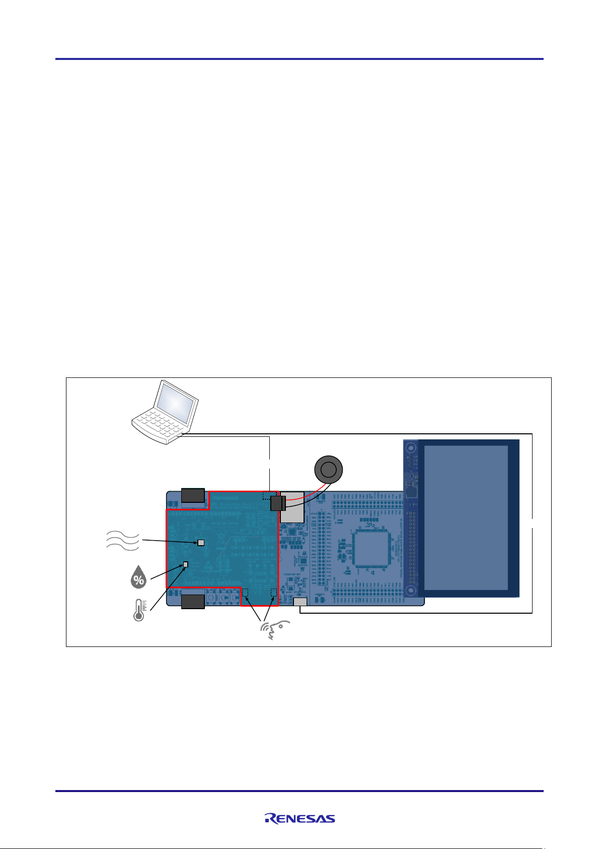
This product provides below features and system configuration.
(1) Voice Recognition by analog output MEMS microphone circuit
Direction forming technology (Beamforming) for voice
(2) Sound playback by D-Amp Driver® circuit(*)
(3) Built-in Temperature and Humidity sensor
(4) Built-in Gas sensor for indoor environment gas detection
• Measurement of Total Volatile Organic Compounds(TVOC)
• Measurement of equivalent CO2(eCO2)
• Measurement of Indoor Air Quality(IAQ)
• Measurement of Odor
(5) Built-in 64Mbit Serial Flash
(6) Expansion connectors (optional)
• External Analog microphone connection
• External I2C Interface device connection
• External UART Interface device connection
(*) D-Amp Driver® is a registered trademark of CRI Middleware Co., Ltd.
RA6M3 HDMI
expansion board
J-Link OB USB
Temperature
measurement
Humidity
measurement
Gas measurement
voice
recognition
Audio
playback
USB
EK-RA6M3G board
Figure 1 System configuration
Page 4
RA6M3 Group RA6M3 HMI Expansion Board
R12AN0106EJ0100 Rev.1.00 Page 4 of 25
Apr.30.2020
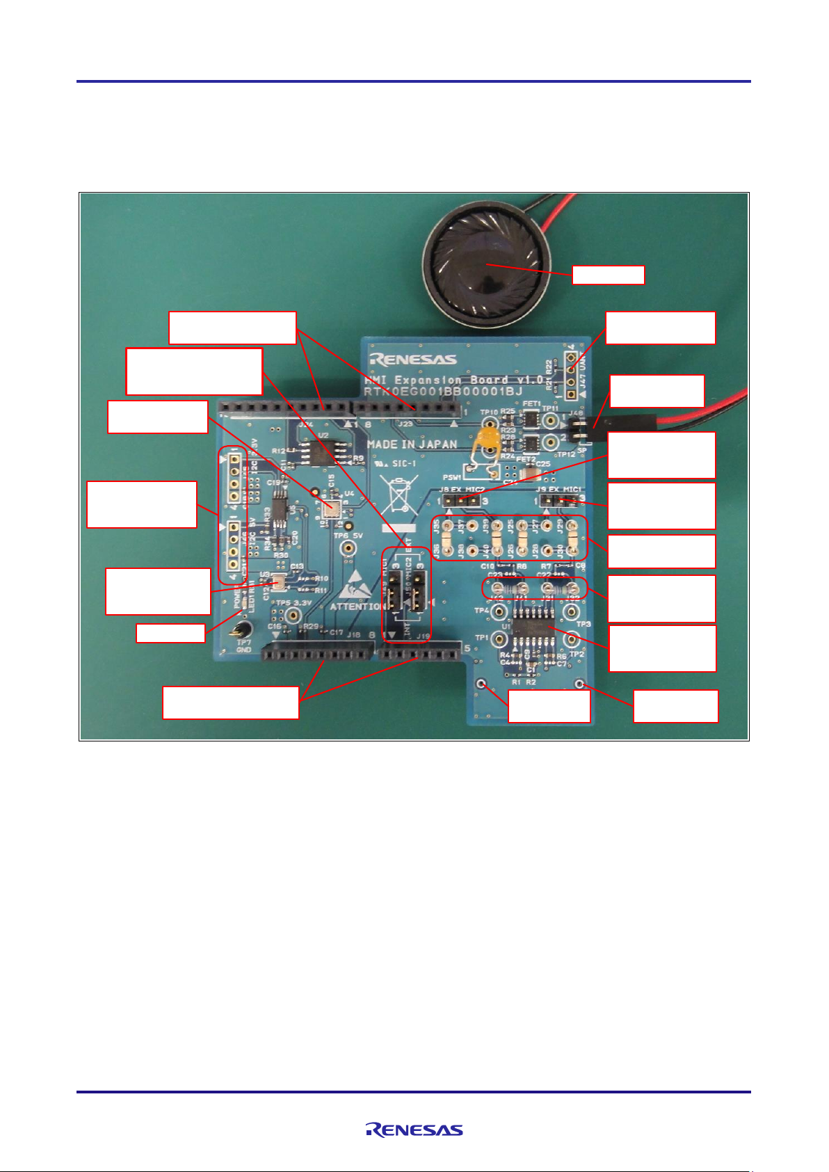
2. Product External Appearance
Speaker
connector
Microphone 1
(back side)
Microphone 2
(back side)
External
microphone 1
(optional)
External
microphone 2
(optional)
Serial expansion
connector (optional)
Sensor expansion
I2C Interface
connector (optional)
Temperature and
humidity sensor
Renesas (IDT)
Gas sensor
Renesas (IDT)
Arduino Uno connector
(Analog & Power)
Arduino Uno connector
(Digital)
External
microphone jumper
External
microphone gain
setting resistor
Internal / external
microphone
selection jumper
Power LED
Speaker
Microphone
amplifier
Renesas
Figure 2 Product External Appearance
Page 5

RA6M3 Group RA6M3 HMI Expansion Board
R12AN0106EJ0100 Rev.1.00 Page 5 of 25
Apr.30.2020
3. Hardware Specifications
Table 1 Hardware Specifications
Item
Description
Remarks
Board size
78.0×80.0[mm]
max external dimension
Power
EK-RA6M3G board J18
3.3V、5V
Serial Flash
MACRONIX International Co.,
Ltd.
MX25R6435FM2IL0
SPI I/F、64Mbit
LED
For Power:
yellow LED 1pc
Microphone
KNOWLES Corp
SPU0410LR5H-QB 2pcs
MEMS microphone,
Omnidirectional,
Sensitivity: -38dBV/Pa,
Analog Output
Amp circuit gain 40dB(x100)
External expansion microphone
(Optional)
MEMS type (Analog output)
Or Electret condenser type
Omnidirectional,
Amp circuit default gain 40dB(x100)
Speaker operation circuit
D-Amp Driver® support H
bridge circuit
Speaker
CUI Devices
CMS-28588N-L152
dimensionsΦ28mm
maximum input power 2W
Impedance 8Ω
Sound Presser Level 88dB SPL(2W、
0.5m)
Humidity and Temperature
Sensor
RENESAS(IDT)
HS3001
I2C IF, 14bit resolution,
Sensor Accuracy
• Temperature ±0.2℃ typ (-10 to
+80℃)
• RH ±1.5%RH typ (10 to 90%RH,
25℃)
Gas Sensor
RENESAS(IDT)
ZMOD4410AI1V
I2C IF, 10~16bit resolution,
Measurement value
• TVOC measurement
• eCO2 measurement
• IAQ measurement
• Odor measurement
Measurement Accuracy
• TVOC±15% typ (after calibration)
• eCO2±25%typ (compared to
NDIR)
I2C Expansion Interface
(Optional)
5V I/F Connector 1pc
3.3V I/F Connector 1pc
UART Expansion Interface
(Optional)
3.3V I/F Connector 1pc
Page 6
RA6M3 Group RA6M3 HMI Expansion Board
R12AN0106EJ0100 Rev.1.00 Page 6 of 25
Apr.30.2020
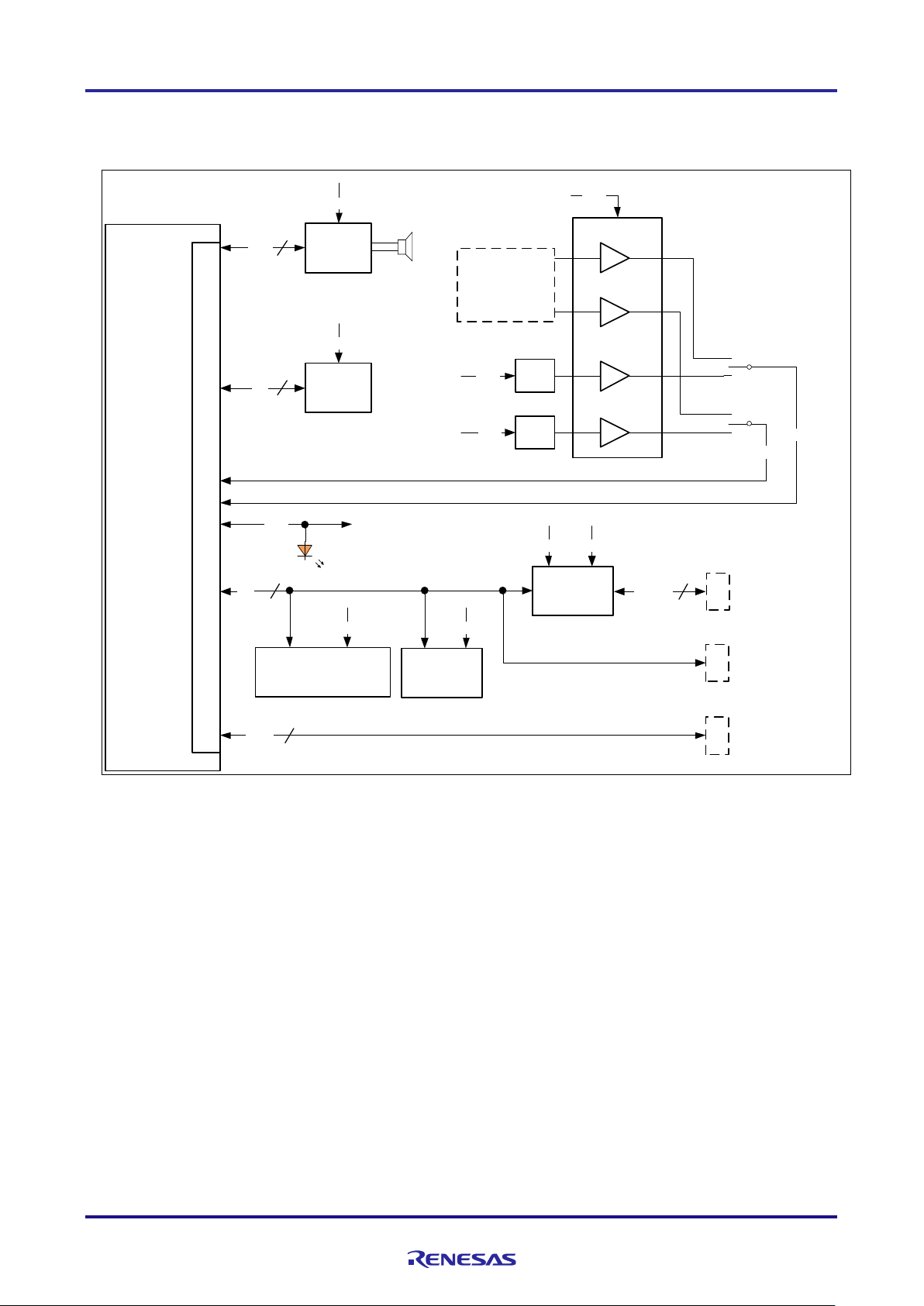
4. Block Diagram
Power supply
LED
H bridge
3.3V
Speaker
D-Amp driver®
external circuit
MIC0
MIC1
MEMS MIC
MIC amplifier
External MIC
(optional)
EX_MIC0
64Mbit
Serial
Flash
3.3V
SPI
Relative Humidity/
Temperature sensor
3.3V
40dB(x100)※
40dB(x100)※
40dB(x100)
40dB(x100)
Gas
sensor
3.3V
Voltage level
translator
3.3V
I2C
5V
I2C(5V)
EK- RA6M3G
board
AN0
AN1
3.3V
3.3V
3.3V
3.3V
3.3V
PWM
Sensor expansion
connector (5V)
(optional)
Sensor expansion
connector (3.3V)
(optional)
UART expansion
connector
(optional)
UART
Arduino Uno Connectors
Jumper
※User configurable
EX_MIC1
Figure 3 Block Diagram
Page 7

RA6M3 Group RA6M3 HMI Expansion Board
R12AN0106EJ0100 Rev.1.00 Page 7 of 25
Apr.30.2020
5. Settings and Connection to the board
5.1 Connects EK-RA6M3 board
As figure 4 shows below, connect RA6M3 HMI expansion board with Arduino Uno connector of EK-
RA6M3G board.
Figure 4 EK-RA6M3G board Connection
Page 8
RA6M3 Group RA6M3 HMI Expansion Board
R12AN0106EJ0100 Rev.1.00 Page 8 of 25
Apr.30.2020
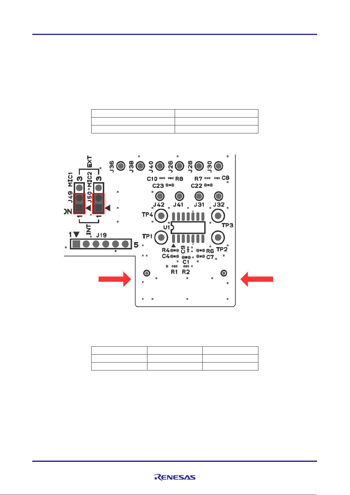
5.2 Microphone
5.2.1 Inside microphone
Table 2 and Figure 5 shows jumper settings. Figure 3 shows direction of microphone when uses
beamforming.
Table 2 Jumper Setting(Inside microphone)
Reference
Setting
J49
Short 1-2pin
J50
Short 1-2pin
MIC1 MIC2
Direction 1 Direction 2
Figure 5 Jumper setting of inside microphone
Table 3 Microphone direction of beamforming(Inside microphone)
Direction
MIC1
MIC2
Direction1
L
R
Direction2
R
L
Page 9
RA6M3 Group RA6M3 HMI Expansion Board
R12AN0106EJ0100 Rev.1.00 Page 9 of 25
Apr.30.2020
5.2.2 External Expansion microphone
External Expansion microphone can be connected to Analog MEMS microphone and Electret condenser
microphone.
Table 4 shows signal of external microphone connector and Table 5 shows Amp gain settings.
Also ,chapter 5.2.2.1 explains Setting of analog MEMS microphone, 5.2.2.2 explains electret condenser
microphone settings.
Table 4 External expansion microphone interface
J9, J8
PIN
Signal name
Type
1
POW/ECMO
POWER/OUT
2
MEMSO
OUT
3
GND
POWER
Table 5 Amp Gain setting of External Expansion microphone
Reference
Gain
U1C
Gain = (Resistance Value J31-J32) / R7
Default:1M / 10K = 100 (40dB)
U1D
Gain = (Resistance Value J41-J42) / R8
Default:1M / 10K = 100 (40dB)
Page 10

RA6M3 Group RA6M3 HMI Expansion Board
R12AN0106EJ0100 Rev.1.00 Page 10 of 25
Apr.30.2020
5.2.2.1 External Analog MEMS microphone
Table 6 and Figure 6 shows Jumper setting of External Analog MEMS microphone. Table 7 shows
microphone direction when beamforming.
Figure 6 Ⓐ part is explained in Table 5.
Table 6 Jumper Setting(External Analog MEMS microphone)
Reference
Settings
J49
Short PIN 2-3
J50
Short PIN 2-3
J35、J36
Implement Jumper resistance
J35-J36
J37、J38
No implementation
J39、J40
Implement Jumper resistance
J39-J40
J25、J26
Implement Jumper resistance
J25-J26
J27、J28
No implementation
J29、J30
Implement Jumper resistance
J29-J30
20mm
Ⓐ
Direction 1 Direction 2
MEMS MIC
EX_MIC2
MEMS MIC
EX_MIC1
Figure 6 Jumper Settings of External MEMS microphone
Table 7 Beamforming Direction(External Expansion microphone)
Direction
EX_MIC1
EX_MIC2
Direction1
R
L
Direction2
L
R
Page 11

RA6M3 Group RA6M3 HMI Expansion Board
R12AN0106EJ0100 Rev.1.00 Page 11 of 25
Apr.30.2020
5.2.2.2 External electret condenser microphone
Table 8 and Figure 7 shows Jumper setting of external electret condenser microphone.
Figure 7 Ⓐ part is explained in Table 5 and refer Table7 for Direction1 and 2.
Table 8 Jumper setting of external electret condenser microphone
Reference
Settings
J49
Short PIN 2-3
J50
Short PIN 2-3
J35、J36
Implement resistance
adopted to electret
condenser microphone
between J35-J33
J37、J38
Implement jumper resistance
between J37-J38
J39、J40
No implementation
J25、J26
Implement resistance
adopted to electret
condenser microphone
between J25-J26
J27、J28
Implement jumper resistance
between J27-J28
J29、J30
No implementation
Electret Condenser
MIC
Ⓐ
20mm
Direction 1 Direction 2
EX_MIC2
EX_MIC1
Figure 7 Jumper setting of external electret condenser microphone
Page 12

RA6M3 Group RA6M3 HMI Expansion Board
R12AN0106EJ0100 Rev.1.00 Page 12 of 25
Apr.30.2020
5.3 Speaker
Table 9 shows speaker connector signals.
Table 9 Speaker Interface
J48
PIN
Signal
Type
1
SPOUT1
OUT
2
SPOUT2
OUT
5.4 Sensor expansion connector(optional)
Table 10 shows sensor expansion 3.3V I2C connector signals. Table 11 shows 5V I2C connector
signals.
Table 10 Sensor Expansion 3.3V I2C Interface
J45
PIN
Signal
Type
1
SCL
IN/OUT
2
SDA
IN/OUT
3
GND
POWER
4
3.3V
POWER
Table 11 Sensor Expansion 5V I2C Interfcace
J46
PIN
Signal
Type
1
SCL
IN/OUT
2
SDA
IN/OUT
3
GND
POWER
4
5V
POWER
5.5 Serial expansion connector(optional)
Table 12 shows serial expansion connector signals.
Table 12 Serial expansion interface
J47
PIN
Signal
Type
1
3.3V
POWER
2
RXD
IN
3
TXD
OUT
4
GND
POWER
Page 13

RA6M3 Group RA6M3 HMI Expansion Board
R12AN0106EJ0100 Rev.1.00 Page 13 of 25
Apr.30.2020
6. Circuit diagram
Figure 8 circuit diagram(1/3)
【*】”NM” shows no implementation
Page 14

RA6M3 Group RA6M3 HMI Expansion Board
R12AN0106EJ0100 Rev.1.00 Page 14 of 25
Apr.30.2020
Figure 8 circuit diagram(2/3)
Page 15

RA6M3 Group RA6M3 HMI Expansion Board
R12AN0106EJ0100 Rev.1.00 Page 15 of 25
Apr.30.2020
Figure 8 circuit diagram(3/3)
Page 16

RA6M3 Group RA6M3 HMI Expansion Board
R12AN0106EJ0100 Rev.1.00 Page 16 of 25
Apr.30.2020
7. Board Layout Diagram
Figure 9 Component Side Silkscreen (top view)
Page 17

RA6M3 Group RA6M3 HMI Expansion Board
R12AN0106EJ0100 Rev.1.00 Page 17 of 25
Apr.30.2020
Figure 10 1st Layer Pattern (top view)
Page 18

RA6M3 Group RA6M3 HMI Expansion Board
R12AN0106EJ0100 Rev.1.00 Page 18 of 25
Apr.30.2020
Figure 11 2nd Layer Pattern (top view)
Page 19

RA6M3 Group RA6M3 HMI Expansion Board
R12AN0106EJ0100 Rev.1.00 Page 19 of 25
Apr.30.2020
Figure 12 3rd Layer Pattern (top view)
Page 20

RA6M3 Group RA6M3 HMI Expansion Board
R12AN0106EJ0100 Rev.1.00 Page 20 of 25
Apr.30.2020
Figure 13 4th Layer Pattern (top view)
Page 21

RA6M3 Group RA6M3 HMI Expansion Board
R12AN0106EJ0100 Rev.1.00 Page 21 of 25
Apr.30.2020
Figure 14 Solder Side Silkscreen (top view)
Page 22

RA6M3 Group RA6M3 HMI Expansion Board
R12AN0106EJ0100 Rev.1.00 Page 22 of 25
Apr.30.2020
Figure 15 External dimensions (Unit:mm)
Page 23

RA6M3 Group RA6M3 HMI Expansion Board
R12AN0106EJ0100 Rev.1.00 Page 23 of 25
Apr.30.2020
8. BOM (parts list)
Table 13 BOM List (1/2)
Item
Parts Type
Reference
PartNo.
Manufacture
Impl
Qty
Remarks
1
64Mbit Flash
Memory
U2
MX25R6435FM2IL0
MACRONIX
Mount
1
8-SOIP
2
Temp and RH
sensor
U3
HS3001
Renesas (IDT)
Mount
1
3
TVOC sensor
U4
ZMOD4410AI1V
Renesas (IDT)
Mount
1
4
I2C level
converter
U5
PCA9306DTR2G
ON
Semiconductor
Mount
1
8-TSSOP
5
Operational
amplifier
U1
ISL28414FBZ
Renesas
Mount
1
14-SOIC
6
MEMS
microphone
MIC1,MIC2
SPU0410LR5H-QB-7
Knowles
Mount
2
7
Composite FET
FET1,FET2
QH8MA2TCR
Rohm
Mount
2
Nch+Pch
8
LED
LED1
SML-D13Y8WT86
Rohm
Mount
1
Golden Yellow
9
Chip Resistor
R23,R24
MCR03EZPJ220
Rohm
Mount
2
22Ω 5%
10
Chip Resistor
R12
MCR03EZPJ330
Rohm
Mount
1
33Ω 5%
11
Chip Resistor
R33,R34
MCR03EZPJ102
Rohm
Mount
2
1KΩ 5%
12
Chip Resistor
R31
MCR03EZPJ122
Rohm
Mount
1
1.2kΩ 5%
13
Chip Resistor
R9,R21,R22,R29
MCR01MZPJ103
Rohm
Mount
4
10kΩ 5%
14
Chip Resistor
R25,R28
MCR03EZPJ103
Rohm
Mount
2
10kΩ 5%
15
Chip Resistor
R30
MCR03EZPJ204
Rohm
Mount
1
200kΩ 5%
16
Chip Resistor
R3,R5,R7,R8
MCR01MZPF1002
Rohm
Mount
4
10kΩ 1%
17
Chip Resistor
R1,R2
MCR01MZPF1003
Rohm
Mount
2
100kΩ 1%
18
Chip Resistor
R4,R6
MCR03EZPFX1004
Rohm
Mount
2
1MΩ 1%
19
Chip Capacitor
C3,C6,C9,C11,C12,C1
3,C15,C16,C17,C18,C
19,C20,C21,C25
EMK105B7104KV-F
Taiyo Yuden
Mount
15
Ceramic
0.1uF/16V
20
Chip Capacitor
C2,C5,C8,C10
EMK105BJ224KV-F
Taiyo Yuden
Mount
4
Ceramic
0.22uF/16V
21
Chip Capacitor
C1
EMK107B7105KA-T
Taiyo Yuden
Mount
1
Ceramic
1uF/16V
22
Chip Capacitor
C24
EMK325AC6476MMP
Taiyo Yuden
Mount
1
Ceramic
47uF/16V
23
Check Terminal
TP1,TP2,TP3,TP4,TP1
0,TP11,TP12,TP13
LC-22G(Yellow)
Mac-Eight
UnMo
unt
8
24
Check Terminal
TP5
LC-22G(Orange)
Mac-Eight
UnMo
unt
1
25
Check Terminal
TP6
LC-22G(Red)
Mac-Eight
UnMo
unt
1
26
Check Terminal
TP7
LC-22G(Black)
Mac-Eight
Mount
1
27
Connector
J8,J9,J49,J50
XJ8B-0311
OMRON
Mount
4
Header 3
position
28
Connector
J19
SSQ-106-03-T-S
Samtec
Mount
1
Receptacle 6
position
29
Connector
J18,J23
SSQ-108-03-T-S
Samtec
Mount
2
Receptacle 8
position
30
Connector
J24
SSQ-110-03-T-S
Samtec
Mount
1
Receptacle 10
position
31
Connector
J48
22-28-6020
MOLEX
Mount
1
Right Angle
Header 2
position
32
Connector
J25,J26,J27,J28,J29,J
30,J31,J32,J35,J36,J3
7,J38,J39,J40,J41,J42
PD-1
Mac-Eight
Mount
16
Socket pin
33
Resetable Fuse
PSW1
PRCP-R025-0-99
Nidec Copal
Electronics
Mount
1
34
Chip Capacitor
C4,C7,C22,C23
-
-
UnMo
unt
4
1608 Pad
35
Chip Resistor
R10,R11 - -
UnMo
unt
2
1608 Pad
Page 24

RA6M3 Group RA6M3 HMI Expansion Board
R12AN0106EJ0100 Rev.1.00 Page 24 of 25
Apr.30.2020
Table 13 BOM List (2/2)
Item
Parts Type
Reference
PartNo.
Manufacture
Impl
Qty
Remarks
36
Connector
J45,J46,J47
XJ8B-0411
OMRON
UnMo
unt
3
37
Resistor
(J31-J32,J41-J42)
MFS1/4CC1004F
KOA
Mount
2
1MΩ 1%
38
Jumper
Resistor
(J25-J26,J29-J30,J35J36,J39-J40)
Z16C
KOA
Mount
4
Jumper
Resistor
39
Shunt
Connector
(J49,J50)
XJ8A-0211
OMRON
Mount
2
40
PCB
-
RTK0EG001BB0000
1BJ
-
- 1
41
Speaker
-
CMS-28588N-L152
CUI inc
Mount
1
8Ω 2W Wire
leads
42
Housing
connector
-
2226A-02
Neltron
Mount
1
Speaker
harness
43
Crimp terminal
-
2226TG
Neltron
Mount
2
Speaker
harness
Page 25

RA6M3 Group RA6M3 HMI Expansion Board
R12AN0106EJ0100 Rev.1.00 Page 25 of 25
Apr.30.2020
Revision History
Rev.
Date
Description
Page
Summary
1.00
Apr 30, 2020
-
First edition issued
Page 26

General Precautions in the Handling of Microprocessing Unit and Microcontroller
Unit Products
The following usage notes are applicable to all Microprocessing unit and Microcontroller unit products from Renesas. For detailed usage notes on the
products covered by this document, refer to the relevant sections of the document as well as any technical updates that have been issued for the products.
1. Precaution against Electrostatic Discharge (ESD)
A strong electrical field, when exposed to a CMOS device, can cause destruction of the gate oxide and ultimately degrade the device operation. Steps
must be taken to stop the generation of static electricity as much as possible, and quickly dissipate it when it occurs. Environmental control must be
adequate. When it is dry, a humidifier should be used. This is recommended to avoid using insulators that can easily build up static electricity.
Semiconductor devices must be stored and transported in an anti-static container, static shielding bag or conductive material. All test and
measurement tools including work benches and floors must be grounded. The operator must also be grounded using a wrist strap. Semiconductor
devices must not be touched with bare hands. Similar precautions must be taken for printed circuit boards with mounted semiconductor devices.
2. Processing at power-on
The state of the product is undefined at the time when power is supplied. The states of internal circuits in the LSI are indeterminate and the states of
register settings and pins are undefined at the time when power is supplied. In a finished product where the reset signal is applied to the external reset
pin, the states of pins are not guaranteed from the time when power is supplied until the reset process is completed. In a similar way, the states of pins
in a product that is reset by an on-chip power-on reset function are not guaranteed from the time when power is supplied until the power reaches the
level at which resetting is specified.
3. Input of signal during power-off state
Do not input signals or an I/O pull-up power supply while the device is powered off. The current injection that results from input of such a signal or I/O
pull-up power supply may cause malfunction and the abnormal current that passes in the device at this time may cause degradation of internal
elements. Follow the guideline for input signal during power-off state as described in your product documentation.
4. Handling of unused pins
Handle unused pins in accordance with the directions given under handling of unused pins in the manual. The input pins of CMOS products are
generally in the high-impedance state. In operation with an unused pin in the open-circuit state, extra electromagnetic noise is induced in the vicinity of
the LSI, an associated shoot-through current flows internally, and malfunctions occur due to the false recognition of the pin state as an input signal
become possible.
5. Clock signals
After applying a reset, only release the reset line after the operating clock signal becomes stable. When switching the clock signal during program
execution, wait until the target clock signal is stabilized. When the clock signal is generated with an external resonator or from an external oscillator
during a reset, ensure that the reset line is only released after full stabilization of the clock signal. Additionally, when switching to a clock signal
produced with an external resonator or by an external oscillator while program execution is in progress, wait until the target clock signal is stable.
6. Voltage application waveform at input pin
Waveform distortion due to input noise or a reflected wave may cause malfunction. If the input of the CMOS device stays in the area between VIL
(Max.) and VIH (Min.) due to noise, for example, the device may malfunction. Take care to prevent chattering noise from entering the device when the
input level is fixed, and also in the transition period when the input level passes through the area between VIL (Max.) and VIH (Min.).
7. Prohibition of access to reserved addresses
Access to reserved addresses is prohibited. The reserved addresses are provided for possible future expansion of functions. Do not access these
addresses as the correct operation of the LSI is not guaranteed.
8. Differences between products
Before changing from one product to another, for example to a product with a different part number, confirm that the change will not lead to problems.
The characteristics of a microprocessing unit or microcontroller unit products in the same group but having a different part number might differ in terms
of internal memory capacity, layout pattern, and other factors, which can affect the ranges of electrical characteristics, such as characteristic values,
operating margins, immunity to noise, and amount of radiated noise. When changing to a product with a different part number, implement a systemevaluation test for the given product.
Page 27

© 2020 Renesas Electronics Corporation. All rights reserved.
Notice
1. Descriptions of circuits, software and other related information in this document are provided only to illustrate the operation of semiconductor products
and application examples. You are fully responsible for the incorporation or any other use of the circuits, software, and information in the design of
your product or system. Renesas Electronics disclaims any and all liability for any losses and damages incurred by you or third parties arising from the
use of these circuits, software, or information.
2. Renesas Electronics hereby expressly disclaims any warranties against and liability for infringement or any other claims involving patents, copyrights,
or other intellectual property rights of third parties, by or arising from the use of Renesas Electronics products or technical information described in this
document, including but not limited to, the product data, drawings, charts, programs, algorithms, and application examples.
3. No license, express, implied or otherwise, is granted hereby under any patents, copyrights or other intellectual property rights of Renesas Electronics
or others.
4. You shall not alter, modify, copy, or reverse engineer any Renesas Electronics product, whether in whole or in part. Renesas Electronics disclaims any
and all liability for any losses or damages incurred by you or third parties arising from such alteration, modification, copying or reverse engineering.
5. Renesas Electronics products are classified according to the following two quality grades: “Standard” and “High Quality”. The intended applications for
each Renesas Electronics product depends on the product’s quality grade, as indicated below.
"Standard": Computers; office equipment; communications equipment; test and measurement equipment; audio and visual equipment; home
electronic appliances; machine tools; personal electronic equipment; industrial robots; etc.
"High Quality": Transportation equipment (automobiles, trains, ships, etc.); traffic control (traffic lights); large-scale communication equipment; key
financial terminal systems; safety control equipment; etc.
Unless expressly designated as a high reliability product or a product for harsh environments in a Renesas Electronics data sheet or other Renesas
Electronics document, Renesas Electronics products are not intended or authorized for use in products or systems that may pose a direct threat to
human life or bodily injury (artificial life support devices or systems; surgical implantations; etc.), or may cause serious property damage (space
system; undersea repeaters; nuclear power control systems; aircraft control systems; key plant systems; military equipment; etc.). Renesas
Electronics disclaims any and all liability for any damages or losses incurred by you or any third parties arising from the use of any Renesas
Electronics product that is inconsistent with any Renesas Electronics data sheet, user’s manual or other Renesas Electronics document.
6. When using Renesas Electronics products, refer to the latest product information (data sheets, user’s manuals, application notes, “General Notes for
Handling and Using Semiconductor Devices” in the reliability handbook, etc.), and ensure that usage conditions are within the ranges specified by
Renesas Electronics with respect to maximum ratings, operating power supply voltage range, heat dissipation characteristics, installation, etc.
Renesas Electronics disclaims any and all liability for any malfunctions, failure or accident arising out of the use of Renesas Electronics products
outside of such specified ranges.
7. Although Renesas Electronics endeavors to improve the quality and reliability of Renesas Electronics products, semiconductor products have specific
characteristics, such as the occurrence of failure at a certain rate and malfunctions under certain use conditions. Unless designated as a high reliability
product or a product for harsh environments in a Renesas Electronics data sheet or other Renesas Electronics document, Renesas Electronics
products are not subject to radiation resistance design. You are responsible for implementing safety measures to guard against the possibility of bodily
injury, injury or damage caused by fire, and/or danger to the public in the event of a failure or malfunction of Renesas Electronics products, such as
safety design for hardware and software, including but not limited to redundancy, fire control and malfunction prevention, appropriate treatment for
aging degradation or any other appropriate measures. Because the evaluation of microcomputer software alone is very difficult and impractical, you
are responsible for evaluating the safety of the final products or systems manufactured by you.
8. Please contact a Renesas Electronics sales office for details as to environmental matters such as the environmental compatibility of each Renesas
Electronics product. You are responsible for carefully and sufficiently investigating applicable laws and regulations that regulate the inclusion or use of
controlled substances, including without limitation, the EU RoHS Directive, and using Renesas Electronics products in compliance with all these
applicable laws and regulations. Renesas Electronics disclaims any and all liability for damages or losses occurring as a result of your noncompliance
with applicable laws and regulations.
9. Renesas Electronics products and technologies shall not be used for or incorporated into any products or systems whose manufacture, use, or sale is
prohibited under any applicable domestic or foreign laws or regulations. You shall comply with any applicable export control laws and regulations
promulgated and administered by the governments of any countries asserting jurisdiction over the parties or transactions.
10. It is the responsibility of the buyer or distributor of Renesas Electronics products, or any other party who distributes, disposes of, or otherwise sells or
transfers the product to a third party, to notify such third party in advance of the contents and conditions set forth in this document.
11. This document shall not be reprinted, reproduced or duplicated in any form, in whole or in part, without prior written consent of Renesas Electronics.
12. Please contact a Renesas Electronics sales office if you have any questions regarding the information contained in this document or Renesas
Electronics products.
(Note1) “Renesas Electronics” as used in this document means Renesas Electronics Corporation and also includes its directly or indirectly controlled
subsidiaries.
(Note2) “Renesas Electronics product(s)” means any product developed or manufactured by or for Renesas Electronics.
(Rev.4.0-1 November 2017)
Corporate Headquarters
Contact information
TOYOSU FORESIA, 3-2-24 Toyosu,
Koto-ku, Tokyo 135-0061, Japan
www.renesas.com
For further information on a product, technology, the most up-to-date
version of a document, or your nearest sales office, please visit:
www.renesas.com/contact/.
Trademarks
Renesas and the Renesas logo are trademarks of Renesas Electronics
Corporation. All trademarks and registered trademarks are the property
of their respective owners.
 Loading...