

Page 1
Application Note
Kit
Operable Long Timer in
LPM
LPM Transition and Clock Changing
at Run-Time
EK-RA2E1
Yes
Yes
EK-RA2L1
Yes
Yes
Renesas RA2 Series
Getting Started with Low Power Applications for
RA2L1
/RA2E1 Group
Introduction
This Application Note describes how you can reduce the effective power consumption of the RA
Microcontroller using Low Power Modes (LPMs). Two accompanying application projects show common use
cases of entering Low Power Modes and configuring the various peripherals to exit the entered mode. Upon
completion of this guide, you will be able to add an LPM module to your own design, configure it correctly for
the target application, and write code using the included application project as a reference and efficient
starting point.
This application note describes:
• LPM module usage in different modes and supported peripherals
• Application overview for the different use cases
• FSP configuration steps for LPM
• Application design highlights
• Importing, loading, and running the application project
• Project migration steps to other RA Kits.
Required Resources
• e2 studio ISDE v2021-01 (21.1.0) or later
• Flexible Software Packag e ( FSP) v2.3.0 or later
• J-Link RTT viewer V6.94 or later
Primary target devices
• EK-RA2L1 kit
• EK-RA2E1 kit
Table 1. RA Kits Tested with LPM Application
R11AN0480EU0101 Rev.1.01 Page 1 of 33
Jan.26.21
Page 2

Renesas RA2 Series Getting Started with Low Power Applications for RA2L1/RA2E1
Group
Contents
1. Application Overview ............................................................................................................... 4
1.1 Low Power Modes .................................................................................................................................. 4
1.1.1 Sleep Mode ........................................................................................................................................... 5
1.1.2 Software Standby Mode ........................................................................................................................ 5
1.1.3 Snooze Mode ........................................................................................................................................ 6
1.2 Activation and Cancel Sources ............................................................................................................... 6
1.3 Peripheral Operation in LPM .................................................................................................................. 6
1.4 Use Case: Changing Clocks at Run-Time .............................................................................................. 6
1.5 Use Case: LPM Transition at Run-Time ................................................................................................ 7
1.6 Use Case: Operable Long Timer in Softwar e Sta ndby Mode ................................................................. 7
2. LPM HAL Module .................................................................................................................... 7
3. FSP Configuration ................................................................................................................... 8
3.1 Components Tab ..................................................................................................................................... 9
3.2 Stacks Tab ............................................................................................................................................. 10
3.3 Module Configuration ............................................................................................................................ 11
3.3.1 LPM Configuration ............................................................................................................................... 11
3.3.1.1 Ac tiv at ion an d Canc elat ion Sour ces ................................................................................................. 11
3.3.1.2 Sleep Mode Configuration ................................................................................................................. 12
3.3.1.3 Software Standby Mode Configuration ............................................................................................. 12
3.3.1.4 Snooze Mode Configuration .............................................................................................................. 13
3.3.2 Timer Configuration ............................................................................................................................. 14
3.3.2.1 RTC Configuration ............................................................................................................................. 14
3.3.2.2 AGT Timer Configuration .................................................................................................................. 15
3.4 Pin Configuration ................................................................................................................................... 17
3.4.1 Pin Configuration in Normal Mode ...................................................................................................... 17
3.4.2 Pin Configuration in LPM ..................................................................................................................... 18
4. Application Architectures ....................................................................................................... 19
4.1 Clock Changing and LPM Transition .................................................................................................... 19
4.2 RTC Timer Operation in LPM ............................................................................................................... 21
4.3 Operable Long Timer in Software Standby Mode ................................................................................. 22
5. Application Code Highlights ................................................................................................... 23
5.1 Clock Source Setup ............................................................................................................................... 23
5.1.1 Handling On-Chip Modules in LPM to Reduce Power Consumption ................................................. 23
5.1.2 Changing System Clock at Run-Time ................................................................................................. 24
6. Importing and Building the Project ......................................................................................... 25
R11AN0480EU0101 Rev.1.01 Page 2 of 33
Jan.26.21
Page 3

Renesas RA2 Series Getting Started with Low Power Applications for RA2L1/RA2E1
Group
7. Running Applications ............................................................................................................. 25
7.1 Board Setups ......................................................................................................................................... 25
7.2 Downloading the Executables ............................................................................................................... 26
7.2.1 Using a debugging interface with e2 studio ......................................................................................... 26
7.2.2 Using J-Link tools ................................................................................................................................ 26
7.2.3 Using Renesas Flash Programmer ..................................................................................................... 26
7.3 User Interface ........................................................................................................................................ 26
7.3.1 LED Indication ..................................................................................................................................... 26
7.3.1.1 Clock Changing and LPM Transition ................................................................................................. 26
7.3.1.2 Operable Long Timer ........................................................................................................................ 26
7.3.2 User Push Button Input ....................................................................................................................... 26
7.3.2.1 Clock Changing and LPM Transition ................................................................................................. 26
7.3.2.2 Operable Long Timer ........................................................................................................................ 26
7.3.3 RTT Console ....................................................................................................................................... 27
7.4 Debugging Low Power Modes .............................................................................................................. 28
7.5 Steps to Run the Application ................................................................................................................. 29
7.5.1 Clock Changing: .................................................................................................................................. 29
7.5.2 LPM Transition .................................................................................................................................... 29
7.5.3 Operable Long Timer .......................................................................................................................... 30
7.6 Measure MCU Current .......................................................................................................................... 31
8. Migrating LPM Applications to Different MCU/Kit ................................................................... 31
9. References ............................................................................................................................ 31
Revision History ............................................................................................................................ 33
R11AN0480EU0101 Rev.1.01 Page 3 of 33
Jan.26.21
Page 4
Renesas RA2 Series Getting Started with Low Power Applications for RA2L1/RA2E1
Group
1. Application Overview
Application Projects accompanying this document serve as references to operate the microcontroller (MCU)
in various Low Power Modes demonstrating different levels of power consumption often required to
maximize battery life.
For ease of understanding the LPM, these appl icati on pr oj ect s cover:
• Different Low Power Modes with different clock settings to showcase each mode
• Operation of different peripherals in an LPM
• Required pin configurations
• Trigger/end source configuration
• A user interface to initiate transition to different LPM states and switch back to Normal mode.
The configuration for each mode is maintained as an independ ent ins ta nc e. Users can use these example
configurations and ch ang e diff er ent settings to trigger/end operation as desired.
In addition to the LPM, the application also supports changing the source clock of the MCU dynamically and
running LPM for these clocks.
Note: In this application note, the project uses the default power supply source from LDO instead of the
optional DC-DC regulator available on the MCU. For more details on using the LPM along with DCDC regulator, see the MCU Hardware User’s Manual.
1.1 Low Pow er Modes
RA MCUs support four different types of LPM depending on the MCU family. These are:
• Sleep mode
• Software Standby mode
• Snooze mode
• Deep Software Standby mode (Available only in selective MCUs).
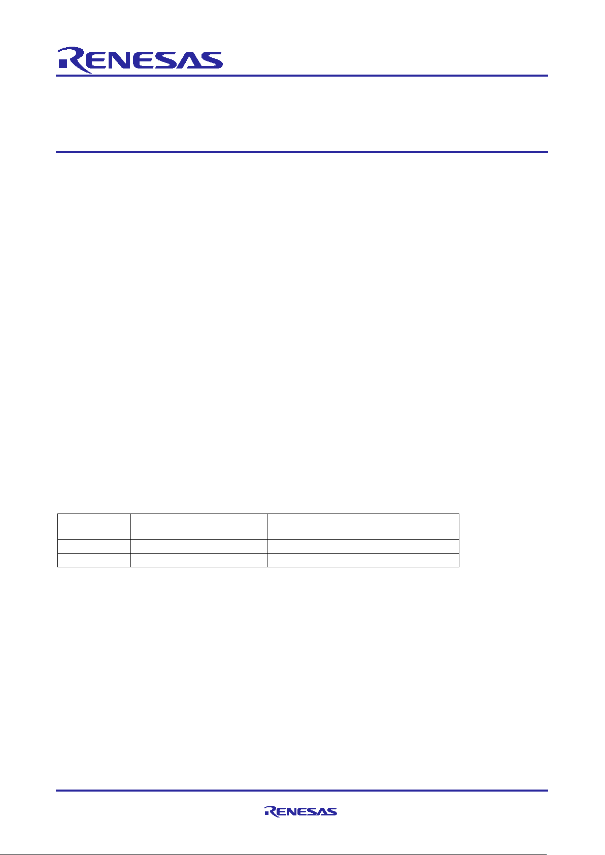
Low power mode transition and triggering sources for RA MCUs are illustrated in Figure 1. For more deta ils
on these transitions, see the User’s Manual for the specific MCU.
Figure 1. LPM Transition Diagram for RA2L1
R11AN0480EU0101 Rev.1.01 Page 4 of 33
Jan.26.21
Page 5
Renesas RA2 Series Getting Started with Low Power Applications for RA2L1/RA2E1
Group
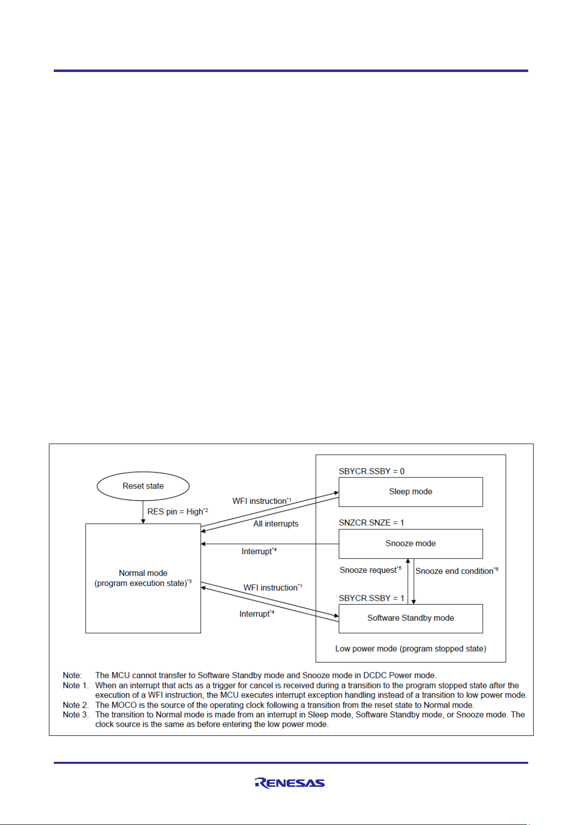
In LPM, the CPU stops, but on-chip peripherals and oscillator states may be operational depending on the
LPM selected. Therefore, their effects on MCU power consumption are very different. The typical current
consumption when the MCU is in a Low Power Mode is found in the MCU Hardware User’s Manual section
on Operating and Standby Current. Figure 2 shows the typical power consumption when the MCU is in a
Low Power Mode vs throughput.
Figure 2. Power Consumption and Throughput of the LPM
In order for the MCU to ent er or exit the LPM, associated special func t ion registers need to be configured.
This app note does not focus on the bit-level configuration details, since the bits can be configured using the
API provided by the FSP. The API provided by the FSP is documented in the FSP User’s Manual. If you
want to explore more details on the LPM and its supported list of peripherals, interrupts, refer to the Low
Power Modes section in the RA MCU Datasheet. Low Power Modes commonly available with RA MCUs are
described next.
MCU also supports different power control modes to reduce the power consumption as part of the LPM.
Power consumption can be reduced in Normal, Sleep, and Snooze mode by selecting an appropriate
operating power control mode according to the operating frequency and voltage.
Four operating power control modes are available:
• High-speed mode
• Middle-speed mode
• Low-speed mode
• Subosc-speed mode
Note: The Power Control mode is not supported in the bundled application projects. For more details on
power control modes, see the User’s Manual for the specific MCUs.
1.1.1 Sleep Mode
An operational CPU is typically the primary cause of power consumption. In Sleep mode, the CPU stops
operating, but the contents of its internal registers are retained. Other peripheral functions in the MCU do not
stop. Available resets or interrupts in Sleep mode can cause the MCU to ca nc el Slee p mode. A ll inter r upt
sources are available in this mode to cancel the Sleep mode. When using an inter rupt to successfully cancel
Sleep mode, you must set the associated IELSRn register before executing a WFI instruction.
1.1.2 Software Standby Mode
In Software Standby mode, the CPU, most of the on-chip peripheral functions and the oscillators stop
operation. However, the contents of the CPU internal registers and the SRAM data, the states of the on-chip
peripheral functions, and the I/O port states are retained. Software Standby mode allows a significant
reduction in power consumption since most of the oscillators stop in this mode.
R11AN0480EU0101 Rev.1.01 Page 5 of 33
Jan.26.21
Page 6

Renesas RA2 Series Getting Started with Low Power Applications for RA2L1/RA2E1
Clock Source
HOCO
High Speed On-Chip Oscillator
MOCO
Medium Speed On-Chip Oscillator
LOCO
Low Speed On-Chip Oscillator
Group
1.1.3 Snooze Mode
The Snooze feature provides operational flexibility to dramatically reduce current consumption. Snooze is an
extension to the Software Standby mode where limited peripheral modules can operate without waking up
the CPU. The Snooze mode can be entered through the Software Standby mode via configured interrupt
sources. Similarly the system can be woken up from Snooze mode by interrupts supported in the Snooze
mode.
1.2 Activation and Cancel Sources
Low power modes are canceled by various interrupt sources such as RES pin reset, power-on reset, voltage
monitor reset, and p erip heral interrupts. Refer to the Low Power Modes section in Renesas RA MCU User’s
Manual for list of interrupt sources for different LPMs.
Only Snooze mode is triggered by a Snooze request to enter Snooze mode from Software Standby mode.
The transitions to other LPMs are done by executing a WFI instruction with appropriate settings in the
Standby Control register (SBYCR).
1.3 Peripheral Operation in LPM
Not all the MCU periphera ls are available in different LPMs. MCU peripherals also have different setting
retention capabilities during the different LPMs, such as contents of the internal registers may be retained in
some LPMs, but the contents may be undefined in other modes. Depending on the requirements of the
application, users are required to choose the peripherals and LPM settings for achieving the maximum power
savings. Users are also required to turn off/disable oscillators and on-chip peripherals that are not clock
gated or powered off to maximize the power savings. Refer to the Low Power Modes section in each RA
MCU User’s Manual: Hardware to understand different oscillator and peripherals available in a specific LPM.
In the next sections we will talk about the use case scenarios for the different LPMs with different clock
settings and peripherals.
1.4 Use Case: Changing Clocks at Run-Time
This application use case describes how to change the RA MCU clock dynamically and set it to different
clock settings supported by the RA MCU using the FSP CGC HAL driver APIs. While the user can configure
the Clock Generation Circuits (CGC) within the MCU using the RA FSP Clock Configurator, in many
applications, where the MCU is eventually powered by a battery, there is an inherent requirement to change
the clock configuration settings as the MCU is running. Based on the desire d set of clock sources, MCU
changes to different clock source and o per ates norm al l y without reboot.
Changing the system clock affects the peripherals, which use derivatives of the system clock as a source
and other clocks in the system. Users are advised to select the dividers as applicable for the system. When
changing the clock, make sure to allow stabilization with the proper settling time. This stabilization time is
designed into the CGC HAL Driver.
This application operates using the user switch input to change the MCU clock mode from the previously
running clock to the desired clock. The new clock settings are applied and displayed via the RTT int er fac e for
the user notification.
Table 2 shows the available user selectable clock settings in the application
Table 2. User Selectable Clock on EK-RA2L1 Board
The sequence of the clock being configured is HOCO→MOCO→LOCO →HOCO. The objective of this use
case is to show the different clock sources which can be changed during run time without halting the MCU.
Changing the clock dynamically is accomplished by using the RA CGC HAL driver API R_CGC_ClocksCfg.
For more details on CGC HAL driver API, refer to the FSP User’s Manual.
R11AN0480EU0101 Rev.1.01 Page 6 of 33
Jan.26.21
Page 7
Renesas RA2 Series Getting Started with Low Power Applications for RA2L1/RA2E1
Clock Source Supported
LPM Supported
HOCO
SLEEP, SW_STND B Y, SNOOZE
MOCO
SLEEP, SW_STNDBY, SNOOZ E
LOCO
SLEEP, SW_STND B Y, SNOOZE
Group
1.5 Use Case: LPM Transition at Run-Time
This use case shows the different LPMs supported by the MCU for the dif feren t cloc k settings.
The application requires user input from the push button switch to change the LPM available for the MCU
and perform transitions as programmed. The supported LPM and its transitions to the different LPMs are
displayed using the RTT interface for notifying the user. The application also showcases the use of few
peripherals, like the AGT timer, and RTC op er ati ng in different LPMs. It also displays the RTC time
information regularly when MCU transitions to the normal mode from the LPM. AGT1 Timer is used in the
Snooze mode to alter nate between Software Standby mode and Snooze mode. RTC Alarm interrupt is used
to cancel the Software Standby mode and ent er normal mode. IRQn (User Switch Interrupt) is used to cancel
the Sleep mode.
The visual indication of the LPM transitio n can also be s een with the User LED on the Board. When the LED
is blinking approximately every 1 seconds, it is running in the Normal mode. If the LED is turned OFF, it is in
an LPM.
Note: More details on the application are explained in the architecture section 4.1 .The peripherals used in
the application are just few of those available for the MCU. For the complete list of peripherals
supported in the LPM, refer to the LPM section of the MCU User’s Hardware Manual.
Different clock sources and LPMs supported for the RA MCUs are shown in Table 3.
Table 3. Clock Sources and Supported LPM for EK-RA2L1 Board
Transitioning to the different LPMs is accomplished by using the RA LPM HAL driver API
R_LPM_LowPowerModeEnter. More details of this API can be found in the FSP User’s Manual.
1.6 Use Case: Operable Long Timer in Software Standby Mode
The Operable Long Timer in Software Standby mode requires a timer that can operate in a Low Power
Mode. The count source of the timer is another element that should be considered carefully as well. In
Renesas RA MCUs, the 16-bit Asynchronous General-Purpose Timer channel 0 (AGT0) and 16-bit
channel 1 (AGT1) can be used in cascade mode to create an 32-bit timer. In the cascade mode, AGT0
underflow interrupt will trigger the counter of AGT1, AGT0 count source can be the sub-clock oscillator or
LOCO clock, which are available in Software Standby mode. The AGT1 Underflow interrupt is used to wake
the MCU up from LPM.
The maximum period of the 16-bit AGT timer channel 0 with the Sub-Clock count source running at 32.768
kHz is approximately 2.0 seconds. The Operable Lo ng Timer with two AGT timer channels in cascade mode
will have a maximum period of approximately 2184.5 hours with a timer resolution of 30.517 µs.
Note: If a longer wakeup time is required, the RTC can be used via the RTC alarm, but here the resolution
of the timer is limited to 1 second.
Note: With RTC Periodic timer interrupt, the resolution of 1/256 sec can be achieved. However, the RTC
periodic timer events cannot be linked to other peripherals with LPM operations.
2. LPM HAL Module
The LPM HAL module in FSP provides a method t o in c lude the LPM driver into the application and to
configure it for different modes. It also allows configuring different trigger/cancel signals as required for LPM
activation/cancellation. FSP also provides essential APIs to configure and place the MCU in Low Power
Modes. It supports the following Low Power Modes:
• Deep Software Standby mode (on supported MCUs)
• Software Standby mode
• Sleep mode
• Snooze mode
R11AN0480EU0101 Rev.1.01 Page 7 of 33
Jan.26.21
Page 8
Renesas RA2 Series Getting Started with Low Power Applications for RA2L1/RA2E1
Group
3. FSP Configuration
When developing an FSP application in e2 studio, first configur e the FSP using the RA Configurator. To
properly configure the FSP, you must have detailed knowledge of both the software design that you will be
implementing, along with the specific hardware it will be running on. For the hardware, this includes the types
of peripherals to be used on the hardware, and the pins they are map ped to, internal or external to the MCU.
From the software perspective, you need to add the HAL modules for the peripherals you use and decide
how many threads will be used, and what additional software objects like semaphores, queues, and so on
that each thread will require. Once you have this information, you will be ready to successfully configure the
FSP for your specific application needs.
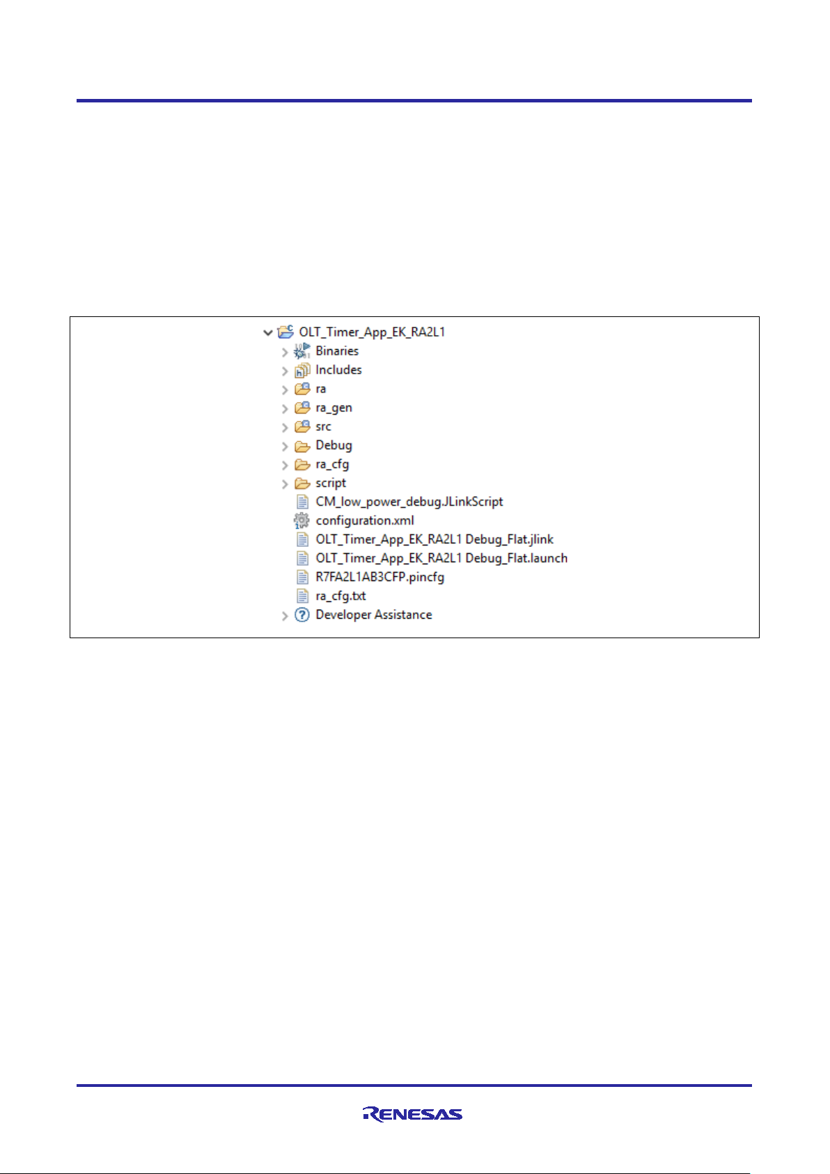
In an application using FSP, the FSP configuration is stored in a file named configuration.xml. Doubleclicking on this file brings up the RA Configuration tab for the project.
Figure 3. configuration.xml on the Project Plane
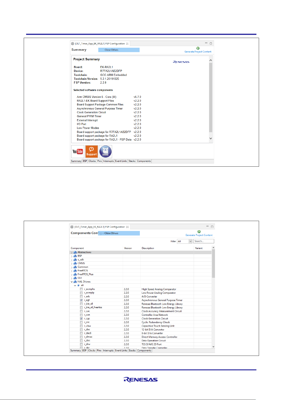
When you build a project from scratch, this configuration tab is where you will perform the initial configuration
of the FSP. As you can see in Figure 4, the RA Configuration pane contains a Summary screen
highlighting the items you may configure, along with a scrolling window that lists all the software components
currently selected for this project. Below this scrolling window are tabs that allow you to tailor the FSP to the
needs of your specific app lic ation . More details on the use of the FSP configurator can be found in the FSP
user’s manual.
For the purposes of this application note, we will highlight a few of the details of the FSP properties such as
the r_lpm driver, r_rtc driver, and r_agt driver modules as they are key components operated in the use
cases provided in the application.
When you have configured the project appropriately, click the Generate Project Content, the green arrow
button above the summary screen, to build all the auto-generated files necessary to implement the
components you defined.
R11AN0480EU0101 Rev.1.01 Page 8 of 33
Jan.26.21
Page 9
Renesas RA2 Series Getting Started with Low Power Applications for RA2L1/RA2E1
Group
Figure 4. Summary of the Operable Long Timer Configuration
3.1 Components Tab
Even though the Components tab is the last tab showing, it is important to visit and verify the configured
components are checked against the desired FSP version. Components are automatically selected when the
modules are added
selected, it is a good process to verify these selections are checked in the Components tab. One of the
advantages of the FSP is that it will only compile the components you choose, thereby reducing the size of
your overall application. As shown in Figure 5, components are broken down into seven categories.
in the Stack tab specific to the application. As the final step to verify the components
Figure 5. Components Tab Categories
R11AN0480EU0101 Rev.1.01 Page 9 of 33
Jan.26.21
Page 10
Renesas RA2 Series Getting Started with Low Power Applications for RA2L1/RA2E1
Category
Component
Version
Description
BSP
ra2l1_ek
2.3.0
RA2L1-EK Board Suppor t Pack age Files
ra2e1_ek
2.3.0
RA2E1-EK Board Support Package Files
CMSIS
CoreM
5.7.0
Arm CMSIS Version5 - Core (M)
Common
fsp_common
2.2.0
Board Support Package Common Files
HAL Drivers
r_cgc
2.3.0
Clock Generation Circuit
r_ioport
2.3.0
I/O Port
r_lpm
2.3.0
Low Power Modes
r_icu
2.3.0
External Interrupt
r_gpt
2.3.0
General PWM Timer
r_agt
2.3.0
Asynchronous General-Purpose Timer
r_rtc
2.3.0
Real Time Clock
Group
You may expand any of the categories by clicking the arrow to the left of the category name. The following
table highlights the selections used for the LPM applications.
Table 4. Components Used in the LPM Applications
Note: This section is for user reference and for read-only purposes. Don’t select or deselect the generated
options by the FSP configurator.
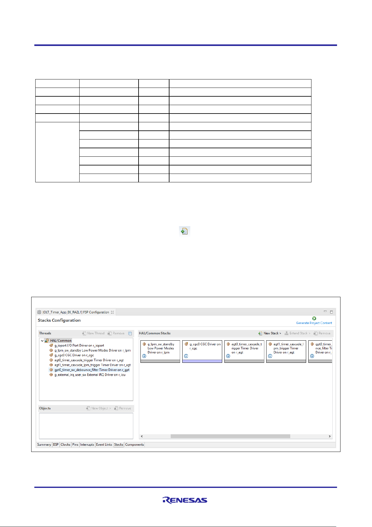
3.2 Stacks Tab
The Stacks tab is where you can add and configure the threads that the FSP automatically creates for your
application. You define a new thread by clicking the button and then entering a unique name for your
new thread. Once you add a new thread, you must define the modules that the thread will use along with any
thread objects that will be used by your application thread.
As an example, if you click the Stacks tab and then single click on the HAL/Common thread, you should
see something like the screen capture shown in Figure 6. This shows that the application requires multiple
drivers, like the r_lpm driver which is the driver for Low Power Modes of Renesas RA MCU. The LPM
applications do not use RTOS, so there is only one HAL/Common thread is available in this type of
application.
R11AN0480EU0101 Rev.1.01 Page 10 of 33
Jan.26.21
Figure 6. Drivers Usage in LPM Application
Page 11
Renesas RA2 Series Getting Started with Low Power Applications for RA2L1/RA2E1
Category
Interrupt Source
Application
Description
Request Source
AGT1_AGTI
Clock Changing and
AGT Channel 1 Underflow Interrupt
End Source
AGT1_AGTI
Clock Changing and
LPM Transition
AGT Channel 1 Underflow Interrupt
Wake/Cancel
AGT1_AGTI
Operable Long Timer
AGT Channel 1 Underflow Interrupt
PORT_IRQ3
Clock Changing and
LPM Transition
External Interrupt 3
RTC_ALM
Clock Changing and
RTC Alarm Interrupt
Group
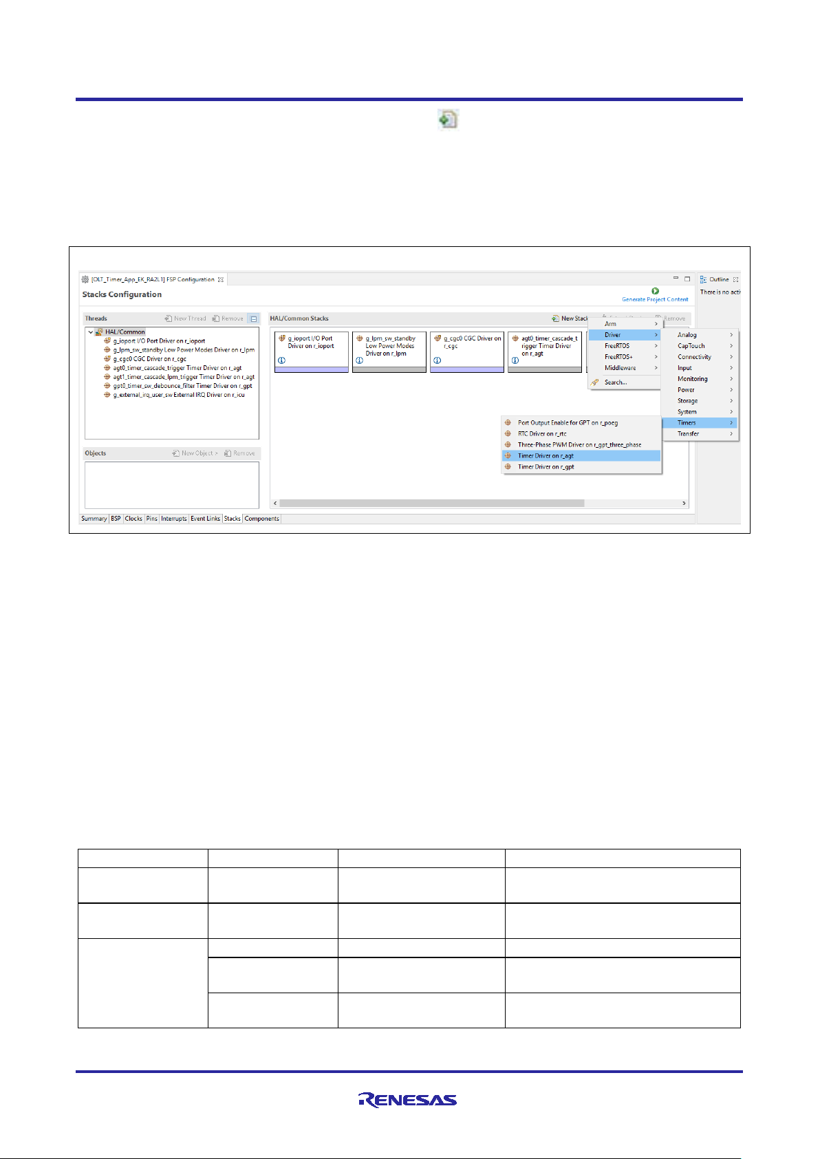
You can add additional modules to a thread by clicking the button. As an example, Figure 7 shows you
how to add an AGT timer. The timer is added by choosing (+) New Stack > Driver > Timers > Timer Driver
on r_agt.
If you pick a module that you have not preselected, the appropriate component for the module will be
automatically selected by FSP for you. If the configurator tool detects errors due to incorrect settings with the
module addition, it presents the module with an error. You may examine the errors by hovering over the
module name.
Figure 7. Adding r_agt Driver to HAL/Common Thread
3.3 Module Configuration
Once you have added a module to your project, you need to configure its properties. The properties are
dependent on the module(s) that you have added. Use the Properties tab to configure them.
3.3.1 LPM Configuration
The LPM applications add the r_lpm driver module as the main component to configure the Renesas RA
MCUs in Low Power Modes, for Sleep, Software Standby, and Snooze. The main settings of Low Power
Modes configures the trigger/cancel sources, different modes.
3.3.1.1 Activation and Cancelation Sources
The cancelation source of an LPM will wake up the MCU from the specific LPM. The request of the Snooze
mode puts the MCU into Snooze mode from Software Standby mode. These sources are interrupt sources.
Refer to the Low Power Modes section in Renesas RA MCU Hardware Manual for more details on what
interrupts are available in the LPM.
Table 5 shows the activation and cancelation sources using in the LPM applications.
Table 5. Activation and Cancelation Source Configuration
LPM Transition
Source
R11AN0480EU0101 Rev.1.01 Page 11 of 33
Jan.26.21
LPM Transition
Page 12

Renesas RA2 Series Getting Started with Low Power Applications for RA2L1/RA2E1
Group
3.3.1.2 Sleep Mode Configuration
Since Sleep mode is canceled by any interrupt, there is no need to set up a cancel source for this mode in
r_lpm driver configuration, as long as there is at least one source of interrupt active in the system. If the LPM
application is using RTOS, the Systick timer must be stopped before entering the Sleep mode because the
Systick interrupt will wake up the MCU. When you are using the RTOS, if the Systick timer is stopped, it must
be restarted after waking up for the proper RTOS kernel operation.
3.3.1.3 Software Standby Mode Configuration
Figure 8 shows how the LPM may be configured to exit Software Standby mode with AGT1 underflow
interrupt as the wake source.
Figure 8. Software Standby Properties Configuration using the Properties Tab
R11AN0480EU0101 Rev.1.01 Page 12 of 33
Jan.26.21
Page 13

Renesas RA2 Series Getting Started with Low Power Applications for RA2L1/RA2E1
Group
3.3.1.4 Snooze Mode Configuration
The Snooze Request source triggers a transition from Software Standby mode to Sno oz e mode. The Snooze
End source cancels Snooze mode and transition the MCU back to Software Standby mode.
The wake source of Software Standby mode will wake up the MCU from both Software Standby and Snooze
modes.
Figure 9 shows how to configure Snooze mode with AGT1 Underflow as both Snooze Request and End
sources.
Figure 9. Snooze Properties Configuration using the Properties Tab
R11AN0480EU0101 Rev.1.01 Page 13 of 33
Jan.26.21
Page 14

Renesas RA2 Series Getting Started with Low Power Applications for RA2L1/RA2E1
Group
3.3.2 Timer Configuration
3.3.2.1 RTC Configuration
The Real Time Clock (RTC) is one of the peripherals which can operate in all the Low Power Modes. The
RTC is primarily used for time keeping, which updates the time independent of MCU in LPM. In this
application, the RTC is used for keeping track of the time in the Clock Changing and LPM Transition
application and to wake up from Software Standby mode via the RTC alarm interrupt. RTC uses the LOCO
as the clock source in the application.
The application displays the RTC time when the MCU transition from LPM to Normal mode. This gives the
indication of the how long the MCU was in LPM and latest time info.
The following Figure 10 shows the configurations of RTC for Time and Alarm. Alarm is used as trigger in the
LPM. The clock source of RTC is LOCO, which is available in Low Power Modes.
Figure 10. RTC Properties Configuration using the Properties Tab
R11AN0480EU0101 Rev.1.01 Page 14 of 33
Jan.26.21
Page 15
Renesas RA2 Series Getting Started with Low Power Applications for RA2L1/RA2E1
Group
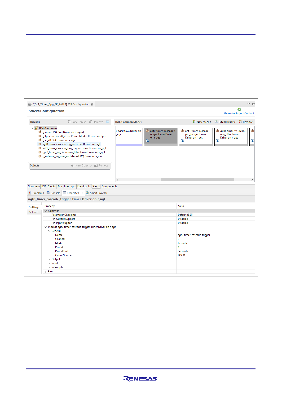
3.3.2.2 AGT Timer Configuration
As mentioner earlier, the Operable Long Timer application in LPM uses AGT timer channel 0 (AGT0) and
AGT timer channel 1 (AGT1) in cascade mode to create a 10-second operable long timer. In this mode,
AGT0 underflow interrupt will trigger the counter of AGT1.
The following figures show the configurations of AGT0 and AGT1. The count source of AGT0 is the SubClock, which is available in Low Power modes, and the count source for AGT1 is the AGT0 underflow
interrupt.
AGT0 is configured in a periodic mode that generates underflow interrupt every second as shown in Figure
11.
Figure 11. AGT0 Properties Configuration using the Properties Tab
R11AN0480EU0101 Rev.1.01 Page 15 of 33
Jan.26.21
Page 16

Renesas RA2 Series Getting Started with Low Power Applications for RA2L1/RA2E1
Group
AGT1 is also configured in a periodic mode with raw count as the period unit shown in Figure 12.
Figure 12. AGT1 Properties Configuration using the Properties Tab
R11AN0480EU0101 Rev.1.01 Page 16 of 33
Jan.26.21
Page 17

Renesas RA2 Series Getting Started with Low Power Applications for RA2L1/RA2E1
Group
3.4 Pin Configuration
The FSP application can support multiple pin configurations. In this application we use two different pin
configurations, one for active mode of operation and other for power saving mode operation. Refer to the
Renesas Flexible Software Package (FSP) User’s Manual on how to configure the FSP Pin Configuration.
3.4.1 Pin Configuration in Normal Mode
The pin configuration in normal mode is the MCU pin functionalities that you want to use in normal operating
condition. Figure 13 s h ows the pin configuration of the EK-RA2L1 kit which is used in normal mo de.
Figure 13. Pin Configuration of EK-RA2L1 Kit in Normal Mode
R11AN0480EU0101 Rev.1.01 Page 17 of 33
Jan.26.21
Page 18

Renesas RA2 Series Getting Started with Low Power Applications for RA2L1/RA2E1
Group
3.4.2 Pin Configuration in LPM
Use the pin configuration in Low Power Modes to reduce power consumption by disabling unused pins ,
which puts them in the input mode. Refer to the “Handling of Unused Pins” section of the MCU Hardware
user manual for more detail s.
Figure 14 shows the pin configuration of the EK-RA2L1 kit in LPM named RA2L1-EK-LPM.pincfg with
unused pins disabled. You may observe that most pins are disabled, except for the IRQ pins, and CGC pins,
which are used to wake up the MCU and provide clock input through the XTAL and EXTAL pins.
Figure 14. Pin Configuration of EK-RA2L1 Kit, operating in LPM
R11AN0480EU0101 Rev.1.01 Page 18 of 33
Jan.26.21
Page 19

Renesas RA2 Series Getting Started with Low Power Applications for RA2L1/RA2E1
Group
4. Application Architectures
The following Figure 15 shows transitions between LPM and normal mode in LPM applications. The WFI
instructions activate LPM, the configured interrupt such as AGT1 underfl ow inter r upt cancels LPM and wakes
up the MCU.
Figure 15. Transition Between LPM and Normal Mode
4.1 Clock Changing and LPM Transition
This application demonstrates the use case where the clock source to the CPU is changed at runtime. It also
demonstrates entering and exiting the different LPM using the API provided by the FSP. Without the
availability of the APIs, a developer would need to configure the registers related to LPM and CGC manually,
thereby adding to development timeline.
The following Figure 16 shows the different clock sources and the associated LPM used in the application
and different transition states. The application implemented using the event driven mechanism. In this event
driven system, events can be user driv en event or system generated event, which are used as the input to
the finite state machine. Two separate state transition tables are used here in the application.
• Clock transition table (clock_transition_table)
• LPM Transition table (lpm_transition_table).
The transition table has the list of actions to be performed based on the events received. For instance, when
user event “Button Press - Long” is received upon power on reset, the finite state machine will start running
and change the clock to HOCO. If user event “Button Press – Short“ is received, the finite state machine will
switch to the LPM state machine and start the LPM operation.
R11AN0480EU0101 Rev.1.01 Page 19 of 33
Jan.26.21
Page 20

Renesas RA2 Series Getting Started with Low Power Applications for RA2L1/RA2E1
Power On
Reset
CPU : Clock Sour ce
HOCO
Clock Sources
Low Power Mode
(A)
(B)
(C)
(a)
CPU : Clock Sour ce
MOSC
CPU : Clock Sour ce
MOCO
CPU : Clock Sour ce
LOCO
CPU : Clock Sour ce
SOSC
(D)
CPU:
Subsystem clock
operation
CPU:
Subsystem clock
operation
Snooze Mode
Sleep Mode
(1)
(2)
(6)
(b)
(c)
(5b) (5a)
CPU : Clock Sour ce
MOCO
CPU : Clock Sour ce
SOSC
Software Standby
Mode
N
o
r
m
a
l
M
o
d
e
(3)
(4)
Normal Mode
Normal Mode
Normal Mode
Clock Change Mode Transition
Low Power Mode - Transition
Internal Reset St ate
(LP)
– Long Press Event
(SP) – Short Press Event
(RTC) – RTC Event
(Timer) – Ti mer Event
(LP)
(LP)
(LP)
(LP)
(LP)
(LP)
(LP)
(SP)
(SP)
(SP)
(SP)
(LP)
/(SP)
(SP)
(RTC)
(RTC)
(Timer)
(Timer)
(d)
Group
Figure 16. Clock Changing and LPM Transi tion
In the above Figure 16, the blue colored oval shaped blocks (B) though (D) represent the different clock
states used in the application, and (a) through (d) labeled arrows are different transition paths it takes when
changing the clock.
The yellow blocks are the different LPM states as applicable to the MCU, and (1) through (6) numbered
arrows, represents the transition path at the different Low Power Modes.
Note: The dotted block represents the Clock Change Mode transition on the left and LPM Transition on the
Note: The Snooze mode is entered via Software Standby mode. For the Snooze mode, from the application
right as shown in Figure 16
perspective, the MCU and LPM drivers hand le t he Sof tw are Stan dby mode internally, while it is
configured for the Snooze mode
Note: The clock can only be changed in the Normal Mode. Changing clock in the LPM mode is not allowed.
Note: In the above Figure 16, for low-end RA devices (R A2 XX) Sleep, Softw ar e Stan db y , and Snooze
modes are supported.
R11AN0480EU0101 Rev.1.01 Page 20 of 33
Jan.26.21
Page 21

Renesas RA2 Series Getting Started with Low Power Applications for RA2L1/RA2E1
List of Event
Description
EV_PB_SHORT_PR
User push button event – “Short Press” – held for 1-2 seconds
EV_PB_LONG_PR
User push button event – “Long Press”– held for 4-6 seconds
EV_PERIODIC_TIMER
AGT1 timer event generate d by timer overflow
EV_RTC_ALARM
RTC Alarm Interrupt generated based on the configured time.
EV_POWER_ON_RESET
Power on Reset event,
Group
Events used in this application are as listed in the Table 6.
Table 6. Events used for the Clock and LPM transitions
4.2 RTC Ti m er Operation in LPM
Realtime clock (RTC) timer operation is an additional feature of the clock changing and LPM transition
application, which showcases the running RTC peripheral during the LPM. Even when the CPU and most
components in the MCU enter Low Power Modes and cease operation, the RTC clock and its timer operate
independently. Updated RTC time information are displayed onto the RTT when it transitions back to the
Normal mode.
RTC Periodic/A larm Inter rupts can be used as signals for transitioning to different LPMs. In this LPM
application project, the RTC Alarm interrupt is used for canceling the Snooze mode/Software Standby mode
and revert to the Normal mode.
Note: The RTC Periodic interrupt can also be used for this event. The RTC Periodic interrupt has a
maximum period of 2 seconds. For demo purp os es, we are avoiding this to showcase the step by
step transition and not to be limited to the 2 seconds. However, the RTC alarm can be configured to
the desired number of seconds.
R11AN0480EU0101 Rev.1.01 Page 21 of 33
Jan.26.21
Page 22

Renesas RA2 Series Getting Started with Low Power Applications for RA2L1/RA2E1
Group
4.3 Oper able Long Timer in Software Standby Mode
The Operable Long Timer Application uses LPM configurations in Software Standby mode. It disables
unused clock and IO ports before entering LPM with the WFI instruction, then places IO ports back to normal
operating condition after w aking up as shown in Figure 17.
LPM is canceled by the Operable Long Timer underflow interrupt, which is created by using AGT0 and AGT1
in cascade mode.
Figure 17. Operable Long Timer Process
R11AN0480EU0101 Rev.1.01 Page 22 of 33
Jan.26.21
Page 23

Renesas RA2 Series Getting Started with Low Power Applications for RA2L1/RA2E1
Group
5. Application Code Hi ghlights
5.1 Clock Source Setup
5.1.1 Handling On-Chip Modules in LPM to Reduce Power Consumption
Oscillators and on-chip modules may be started automatically after MCU reset and be still runn ing in LPM
modes. Therefore, to reduce MCU power consumption, you should disable these modules before entering
LPM.
Unused IO ports in LPM other than in Deep Software Stan dby mode shou ld be p ut into input mode before
entering the LPM by using the g_bsp_pin_lpm_cfg, which is generated from the RA2L1-EK-
LPM.pincfg. The following code fragments highlight the steps in the application to reduce MCU power
consumption before placing MCU in LPM and restoring the IO port settings after waking it up.
Open and configure the LPM.
Place th e MCU in the LPM.
Figure 18. Put Unused IO ports in Input Mode
Figure 19. Open and Configure the LPM
Figure 20. Place the MCU in the LPM
R11AN0480EU0101 Rev.1.01 Page 23 of 33
Jan.26.21
Page 24

Renesas RA2 Series Getting Started with Low Power Applications for RA2L1/RA2E1
Group
Put IO port in normal mode by configuring it using the g_bsp_pin_cfg generated from the RA2L1EK.pincfg after exiting from LPM.
Figure 21. Place IO Ports in Normal Mode
The following code stops the LOCO clock when it is not used as count source for AGT0 as shown in Figure
22.
Figure 22. Stop LOCO Clock when It is Unused
5.1.2 Changing System Clock at Run-Time
When the MCU powers up, the default clock will be the configured clock as part of the BSP. Selecting the
clock for the application is done through the FSP configurator using the clock tree, which is available in the
clocks tab.
In the changing clock use case application, the current running system clock is read via the
R_CGC_SystemClockGet API and a new system clock source is configured. The following code is used for
reading the currently running system clock shown in Figure 23.
Figure 23. Read the running System Clock
In order to configure the new source for the system clock, proper divisors are required so that the peripherals
get the permitted range of frequencies. Users need to calculate this based on the peripherals used in the
application. The new system clock is configured via the API R_CGC_ClocksCfg.
Also, the clock sources need to be started if they are not already running. This is done using the API
R_CGC_ClockStart as shown in the Figure 24.
Figure 24. Starting the Clock Source
R11AN0480EU0101 Rev.1.01 Page 24 of 33
Jan.26.21
Page 25

Renesas RA2 Series Getting Started with Low Power Applications for RA2L1/RA2E1
Switch
Setting
J8
Jumper on pins 1-2
J9
Open
J29
Jumper on pins 5-6
J29
Jumper on pins 7-8
J6
Open
Group
6. Importing and Building the Project
To bring the applications into the e2 studio ISDE, follow these steps:
1. Launch e
2. In the workspace launcher, browse to the workspace location of your choice.
3. Close the Welcome window.
4. In the ISDE go to File > Import.
5. In the Import Dialog Box, pick Existing Projects into Workspace.
6. Select the root directory of your workspace (where you placed the project).
7. Select the project you wish to import and click Finish.
8. Click on Generate Project Content on the FSP configurator window.
9. Now build the project.
2
studio ISDE.
7. Running Applications
To connect and run the code, follow these steps:
7.1 Board Setups
The EK-RA2L1 kit contains a few switch settings which must be configured prior to running the application
associated with this application note. In addition to these switch settings, it has a USB debug port and
connectors to access the J-Link
®
programming interfac e.
Table 7. Switch settings for EK-RA2L1
R11AN0480EU0101 Rev.1.01 Page 25 of 33
Jan.26.21
Figure 25. EK-RA2L1 Kit
Page 26

Renesas RA2 Series Getting Started with Low Power Applications for RA2L1/RA2E1
Group
7.2 Downloading the Executables
The executable file may be programmed into the target MCU through any one of three means.
7.2.1 Using a debugging interface with e2 studio
Instructions to program the executable binary are found in the latest RA FSP User Manual. See Section
Starting Development > e2 studio ISDE User Guide > Tutorial: Your First RA MCU Project > Debug the
Blinky Project.
This is the preferred method for programming as it allows for additional debugging functionality available
through the on-chip deb ugg er.
7.2.2 Using J-Link tools
SEGGER J-Link Tools such as J-Flash, J-Flash Lite, and J-Link Commander can be used to program the
executable binary into the target MCU. Refer to User Manuals UM08001 and UM08003 on www.segger.com
7.2.3 Using Renesas Flash Programmer
The Renesas Flash Programmer provides usable and functional support for programming the on-chip flash
memory of Renesas microcontrollers in each phase of development and mass production. The software
supports all RA MCUs and software user’s manual is available online:
https://www.renesas.com/us/en/software-tool/renesas-flash-programmer-programming-gui#documents
.
7.3 User Interface
The user interface to interact with the application is shown below. The Operable Long Timer applica tion uses
the LED and user push button switch. Whereas the Cloc k Changing and LPM Transition application uses the
RTT interface in addition to the LED and push button switch.
.
7.3.1 LED Indication
7.3.1.1 Clock Changing and LPM Transition
The Clock Changing and LPM Transition application uses LED1 to indicate the board initialization status,
error condition, and normal mode operation. In the Sleep, Software Standby, and Snooze modes, LED1 will
be turned off. In the Normal mode, this LED1 will blink every second. If any error condition occurs the LED1
will be turned ON.
7.3.1.2 Operable Long Timer
The Operable Long Timer application uses LED1 to indicate the normal mode. In the Normal mode, this
LED1 will blink. In the Software Standby mode, LED1 will be turned off.
7.3.2 User Push Button Input
7.3.2.1 Clock Changing and LPM Transition
Push button switch S1 input is mainly used for transitioning to different MCU clocks and transitioning to
different LPMs. For the Clock Changing and LPM Transition application, the same switch has dual
functionality. If the switch is held under 1–2 seconds, it is considered a short press . If the switch is held for 3–
6 seconds, it is considered a long press. A long press event is used for changing the Clock source
dynamically and a short press event is used for the LPM mode transition.
Note: A long press event during the LPM will not change the system clock source to a different clock, but
instead has a different role: to exit the LPM and go back to the Normal mode.
7.3.2.2 Operable Long Timer
In the application, press ing the push button switch S1 will set the Software Stand by mode. The AGT1
underflow interrupt will cancel the LPM in 10 seconds.
R11AN0480EU0101 Rev.1.01 Page 26 of 33
Jan.26.21
Page 27
Renesas RA2 Series Getting Started with Low Power Applications for RA2L1/RA2E1
Group
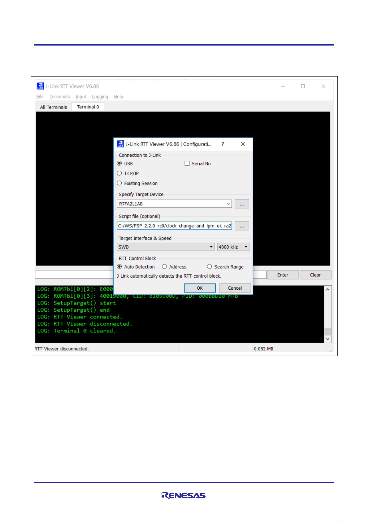
7.3.3 RTT Console
The RTT console comes in handy to view the application messages while running/debugging the application.
While using the RTT console, the debugger script for the LPM needs to be selected as shown in Figure 26.
Figure 26. RTT Console for User Print Messages
R11AN0480EU0101 Rev.1.01 Page 27 of 33
Jan.26.21
Page 28

Renesas RA2 Series Getting Started with Low Power Applications for RA2L1/RA2E1
Group
7.4 Debugging Low Power Modes
By default, it is not possible to debug the low power modes of an RA device. If an application tries to enter
sleep mode, pending a peripheral interrupt to wake it, then this will not happen as it will be woken almost
immediately by a debug interrupt.
If the application tries to enter software mode, then the connection between the CPU and the IDE will be lost,
closing the debug session within the IDE.
However, if the supplied debug script is specified, then it will be possible to debug the low power modes.
These scripts are used for the purpose of demonstrating the LPM. Note, that even though this will allow you
to develop your application, it will not allow you to measure accurate Icc figures, as you will be measuring the
Icc of the on-chip debug circuit. Once you have created your low power application, accurate Icc figures can
be measured with the OCD disabled.
The low-power script also allows for the RTT application to be used. While debug g ing the app lica tio n,
configure the debugger as shown in Figure 27. With these modifications one can use the RTT without getting
disconnected during the LPM.
Note: The script is attached as part of this project and the debugger is pointing to the same location.
Figure 27. Debugger Settings for LPM Application Debugging
R11AN0480EU0101 Rev.1.01 Page 28 of 33
Jan.26.21
Page 29
Renesas RA2 Series Getting Started with Low Power Applications for RA2L1/RA2E1
Events
System Clock
User Button – Long Press
User Button – Short Press
HOCO
oscillator)
Changes the System Clock
Exits the Clock State Machine and enters the
HOCO.
MOCO
oscillator)
Changes the System Clock
Exits the Clock State Machine and enters the
MOCO.
LOCO
oscillator)
Changes the System Clock
Exits the Clock State Machine and enters the
LOCO.
Group
7.5 Steps to Run the Application
The following table shows the steps to run the Clock Changing and LPM Transition application. On power up,
when the board is connected to RTT, it w i ll disp lay th e welcom e message. To change the clock/LPM and run
through the different use cases in this application, use the following tables as reference. These tables have
the list of events, current mode, and refers the new transition states and the expected outcome.
7.5.1 Clock Changing:
The user button has two functions, based on how long you press and hold it. In the clock changing mode, the
user button pressed and held for 3-6 seconds selects the different system clocks for the MCU. Whereas the
user button pressed and held for 1-2 seconds exits the clock changing mode and enters into LPM for the
configured clock. The details are as shown in Table 8.
Table 8. Clock Mode Transition Table
(High speed on-chip
(Medium speed on-chip
(Low speed on-chip
to MOCO
to LOCO
to HOCO
LPM State Machine for the configured clock
LPM State Machine for the configured clock
LPM State Machine for the configured clock
7.5.2 LPM Transition
In the LPM application, the user switch has two functionalities based on how long you pressed, held, and
released it. If the MCU is in the LPM mode (Sleep) and the user button is pressed, held, and released, the
MCU exits the LPM mode and enters the Normal mode whether it was a short press or long press. Whereas
the behavior is different when the MCU is in Normal mode.
When the MCU is in Normal mode, if the user button is pressed, held for 1-2 seconds, and released, MCU
exits the Normal mode and enters (Sleep or Software Standby or Snooze) modes depending on the previous
transition states. Whereas if the switch is pressed, held, and released for 3-6 seconds, MCU exits the LPM
transition setting mode and enters the Clock setting mode. Also the user switch has no effect during the LPM
modes (Software Standby or Snooz e).
Timer events cancel the Software Standby and Sn ooze modes and puts the MCU back to Normal mode.
The details of the switch events and timer events are tabulated in Table 9.
R11AN0480EU0101 Rev.1.01 Page 29 of 33
Jan.26.21
Page 30
Renesas RA2 Series Getting Started with Low Power Applications for RA2L1/RA2E1
Events
Low Power
Modes
User Button – Long Press
User Button – Short
Press
Timer Event
Normal
Exits the LPM transition State
State Machine
Enters the Sleep mode
Not Applicable
Sleep
Exits the Sleep mode and enters the
Exits the Sleep mode
mode
Not Applicable
Normal
Exits the LPM transition State
Exits the Normal mode
mode
Not Applicable
Software
Not Applicable
Not Applicable
Exits the Software
mode
Normal
Standby)
Exits the LPM transition State
Exits the Normal mode
mode
Not Applicable
Snooze with
Not Applicable
Not Applicable
Exits the Snooze with
mode
Events
Low Power Modes
User Button – Press
Timer Event – AGT1_AGTI
Normal
Enters Software Standby Mode
Not Applicable
Software Standby
Not Applicable
Exits the Software Standby mode and enters the
Group
Table 9. LPM Transition Table
Machine and enters the Clock Mode
(From Sleep)
Standby
(From
Software
Software
Standby
Normal mode
Machine and enters the Clock Mode
State Machine
Machine and enters the Clock Mode
State Machine
and enters the Normal
and enters the
Software Standby
Standby mode and
Enters the Normal
and enters the Snooze
with Software Standby
Software Standby mode
and Enters the Normal
7.5.3 Operable Long Timer
In the Operable Long Timer application, the user button is used to enter Software Standby mode from
Normal mode. AGT1 underflow interrupt is used to exit the LPM modes.
Table 10 shows the transition sequence and associated events used in the Operable Long Timer application.
Table 10. LPM Transition Table in Operable Long Timer Application
Normal Mode
R11AN0480EU0101 Rev.1.01 Page 30 of 33
Jan.26.21
Page 31

Renesas RA2 Series Getting Started with Low Power Applications for RA2L1/RA2E1
Group
7.6 Measure MCU Current
The following steps are required to measure MCU current on EK-RA2L1, which is supported by the LPM
applications:
• Power cycle the board after downloading the LPM projects.
• Measure the voltage drops across R3 and calculate MCU's operating and standby current (ICC).
Replace R3 by a bigger resistor if needed.
To measure the ICC current directly, connect a multimeter between the +3V3 and +3V3_MCU pins on the kit
connectors after removing the R3 resistor.
Note: To measure MCU current in total, which includes ICC and analog power supply current (IAVCC0),
follow the below steps on EK-RA2L1 board
• Cut the trace-cut jumper E3.
• Connect J4-2 to J3-11.
8. Migrating LPM App lications to Differe n t MCU /Kit
Even though the LPM applications are created for the Renes as EK-RA2L1 kit, they are designed to easily
migrate to other Renesas RA Kits. For more deta ils , refer “Migrating LPM Applications to Different MCU/Kit”
section 8 in the Getting Started with LPM Application Note for the EK-RA6M3 Board included as part of the
LPM bundle.
9. References
• Renesas FSP User’s Manual: https://renesas.github.io/fsp
• Renesas RA MCU Datasheets: See http://renesas.com/ra and select the relevant MC U
• LPM Example Projects on Renesas RA GitHub: https://github.com/renesas/ra-fsp-examples
R11AN0480EU0101 Rev.1.01 Page 31 of 33
Jan.26.21
Page 32

Renesas RA2 Series Getting Started with Low Power Applications for RA2L1/RA2E1
RA Product Information
www.renesas.com/ra
RA Product Support Forum
www.renesas.com/ra/forum
RA Flexible Software Package
www.renesas.com/FSP
Renesas Support
www.renesas.com/support
Group
Website and Support
Visit the following vanity URLs to learn about key elements of the RA family, download components and
related documentation, and get support.
R11AN0480EU0101 Rev.1.01 Page 32 of 33
Jan.26.21
Page 33

Renesas RA2 Series Getting Started with Low Power Applications for RA2L1/RA2E1
Rev.
Date
Description
Page
Summary
1.00
Dec.3.20
-
Initial version supporting EK-RA2L1
1.01
-
Updated for EK-RA2E1
Group
Revision History
Jan.26.21
R11AN0480EU0101 Rev.1.01 Page 33 of 33
Jan.26.21
Page 34

Corporate Headquarters
Contact information
www.renesas.com
Trademarks
of their respective owners.
Notice
1. Descriptions of circuits, software and other related information in this document are provided only to illustrate the operation of semiconductor products
and application examples. You are fully responsible for the incorporation or any other use of the circuits, software, and information in the design of you r
product or system. Renesas Electronics disclaims any and all liability for any losses and damages incurred by you or third parties arising from the use
of these circuits, software, or information.
2. Renesas Electronics hereby expressly disclaims any warranties against and liability for infringement or any other claims involvi ng pat ents, copyrights,
or other intellectual property rights of third parties, by or arising from the use of Renesas Electronics products or technical information described in this
document, includin g but not lim ited to, the product data, drawings, charts, programs, algorithms, and application examples.
3. No license, express, implied or otherwise, is granted hereby under any patents, copyrights or other intellectual property rights of Renesas Electronics
or others.
4. You shall not alter, modify, copy, or reverse engineer any Renesas Electronics product, whether in whole or in part. Renesas Electronics disclaims any
and all liability for any losses or damages incurred by you or third parties arising from such alteration, modification, copying or reverse engineering.
5. Renesas Electronics products are classified according to the following two quality grades: “Standard” and “High Quality”. The intended applications for
each Renesas Electronics product depends on the product’s quality grade, as indica te d bel ow.
"Standard": Computers; office equipment; communications equipment; test and measurement equipment; audio and visual equipment; home
"High Quality": Transportation equipment (automobiles, trains, ships, etc.); traffic control (traffic lights); large-scale communication equipment; key
Unless expressly designated as a high reliability product or a product for harsh environments in a Renesas Electronics data sheet or other Renesas
Electronics document, Renesas Electronics products are not intended or authorized for use in products or systems that may pose a direct threat to
human life or bodily injury (artificial life support devices or systems; surgical implantations; etc.), or may cause serious property damage (sp ace
system; undersea repeaters; nuclear power control systems; aircraft control systems; key plant systems; military equipment; etc.). Renesas Electronics
disclaims any and all liability for any damages or losses incurred by you or any third parties arising from the use of any Renesas Electronics product
that is inconsistent with any Renesas Electronics data sheet, user’s manual or other Renesas Electronics document.
6. When using Renesas Electronics products, refer to the latest product information (data sheets, user’s manuals, application notes, “General Notes for
Handling and Using Semiconductor Devices” in the reliability handbook, etc.), and ensure that usage conditions are within the ranges specified by
Renesas Electronics with respect to maximum ratings, operating power supply voltage range, heat dissipation characteristics, installation, etc. Renesas
Electronics disclaims any and all liability for any malfunctions, failure or accident arising out of the use of Renesas Electronics products outside of such
specified ranges.
7. Although Renesas Electronics endeavors to improve the quality and reliability of Renesas Electronics products, semiconductor products have specific
characteristics, such as the occurrence of failure at a certain rate and malfunctions under certain use conditions. Unless designated as a high reliability
product or a product for harsh environments in a Renesas Electronics data sheet or other Renesas Electronics document, Renesas Electronics
products are not subject to radiation resistance design. You are responsible for implementing safety measures to guard against the possibility of bodily
injury, injury or damage caused by fire, and/or danger to the public in the event of a failure or malfunction of Renesas Electronics products, such as
safety design for hardware and software, including but not limited to redundancy, fire control and malfunction prevention, appropriate treatment for
aging degradation or any other appropriate measures. Because the evaluation of microcomputer software alone is very difficult and impractical, you are
responsible for evaluating the safety of the final products or systems manufactured by you.
8. Please contact a Renesas Electronics sales office for details as to environmental matters such as the environmental compatibility of each Renesas
Electronics product. You are responsible for carefully and sufficiently investigating applicable laws and regulations that regulate the inclusion or use of
controlled substances, including without limitation, the EU RoHS Directive, and using Renesas Electronics products in compliance with all these
applicable laws and regulations. Renesas Electronics disclaims any and all liability for damages or losses occurring as a result of your noncompliance
with applicable laws and regulations.
9. Renesas Electronics products and technologies shall not be used for or incorporated into any products or systems whose manufacture, use, or sale is
prohibited under any applicable domestic or foreign laws or regulations. You shall comply with any applicable export control laws and regulations
promulgated and administered by the governments of any countries asserting jurisdiction over the parties or transactions.
10. It is the responsibility of the buyer or distributor of Renesas Electronics products, or any other party who distributes, disposes of, or otherwise sells or
transfers the product to a third party, to notify such third party in advance of the contents and conditions set forth in this document.
11. This document shall not be reprinted, reproduced or duplicated in any form, in whole or in part, without prior written consent of Renesas Electronics.
12. Please contact a Renesas Electronics sales office if you have any questions regarding the information contained in this document or Renesas
Electronics products.
(Note1) “Renesas Electronics” as used in this document means Renesas Electronics Corporation and also includes its directly or indirectly controlled
(Note2) “Renesas Electronics product(s)” means any product developed or manufactured by or for Renesas Electronics.
subsidiaries.
electronic appliances; machine tools; personal electronic equipment; industrial robots; etc.
financial terminal systems; safety control equipment; etc.
(Rev.4.0-1 Novembe r 201 7)
TOYOSU FORESIA, 3-2-24 Toyosu,
Koto-ku, Tokyo 135-0061, Japan
Renesas and the Renesas logo are trademarks of Renesas Electronics
Corporation. All trademarks and registered trademarks are the property
For further information on a product, technology, the most up-to-date
version of a document, or your ne are s t sales office, please visit:
www.renesas.com/contact/
.
© 2021 Renesas Electronics Corporation. All rights reserved.
 Loading...