

Page 1

Application Note
R01AN5795EJ0100 Rev.1.00 Page 1 of 24
Mar.31.21
RA2A1 Group
Board Control Program for QE for AFE
Introduction
The control program operates on RA2A1 on the EK-RA2A1 evaluation board, communicates commands with
the AFE development support tool ‘QE for AFE’, and can set registers for analog IP and obtain the A/D
conversion values as shown below.
⎯ 24-Bit Sigma-Delta A/D Converter (SDADC24)
⎯ 16-Bit A/D Converter (ADC16)
⎯ 12-Bit D/A Converter (DAC12)
⎯ 8-Bit D/A Converter (DAC8)
⎯ Operational Amplifier (OPAMP)
Target Device
RA2A1 (R7FA2A1AB3CFM)
Board to Be Operated
EK-RA2A1 Evaluation Kit for RA2A1 Microcontroller Group
Available Communication I/F:
⎯ USB PCDC Communication
⎯ SCI UART Communication: A separate USB-UART adapter is required.
Page 2

RA2A1 Group Board Control Program for QE for AFE
R01AN5795EJ0100 Rev.1.00 Page 2 of 24
Mar.31.21
Contents
1. Overview ................................................................................................................................. 3
1.1 System Overview ..................................................................................................................................... 3
1.2 Operation Confirmation Environment ...................................................................................................... 4
1.3 File Configurations................................................................................................................................... 5
1.4 Peripherals to Use ................................................................................................................................... 6
1.5 Pin Settings ............................................................................................................................................. 7
1.5.1 Pin List ................................................................................................................................................... 7
1.5.2 ADC16 Precautions When Using .......................................................................................................... 8
1.5.3 How LED1 Work .................................................................................................................................... 8
1.6 Communication Specifications ................................................................................................................ 9
1.6.1 Serial Communication Settings ............................................................................................................. 9
1.6.2 Connecting USB-UART adapter during UART communication ............................................................ 9
1.7 About Project Source Changes ............................................................................................................... 9
1.8 Related Documentation ........................................................................................................................... 9
2. How to Write FW ................................................................................................................... 10
2.1 Write Using e2 studio Integrated Development Environment (IDE) ...................................................... 10
2.1.1 Import Procedure ................................................................................................................................. 10
2.1.2 Notes on Building Project for USB PCDC Communication ................................................................. 10
2.1.3 Notes on Building Project for SCI UART Communication ................................................................... 11
2.2 Writing using Renesas Flash Programmer ........................................................................................... 12
3. Run Project ............................................................................................................................ 15
3.1 Connecting to PC .................................................................................................................................. 15
3.1.1 USB PCDC Communication ................................................................................................................ 15
3.1.2 USB PCDC Communication ................................................................................................................ 15
3.2 Launch QE for AFE ............................................................................................................................... 16
3.2.1 Preparation .......................................................................................................................................... 16
3.2.2 Launching QE for AFE and Connecting to Target Board .................................................................... 16
3.2.3 Operation Confirmation ....................................................................................................................... 16
3.3 Sample Configuration File ..................................................................................................................... 17
3.3.1 Configuration Overview of Sample Configuration File ........................................................................ 18
3.3.2 Setting Procedure after Import ............................................................................................................ 19
3.3.2.1 Project for USB PCDC Communication ............................................................................................ 19
3.3.2.2 Project for SCI UART Communication .............................................................................................. 20
3.4 QE for AFE Tuning Execution ............................................................................................................... 21
3.4.1 Writing Setting Value ........................................................................................................................... 21
3.4.2 Tuning Operation ................................................................................................................................. 22
Revision History ............................................................................................................................ 24
Page 3
RA2A1 Group Board Control Program for QE for AFE
R01AN5795EJ0100 Rev.1.00 Page 3 of 24
Mar.31.21
1. Overview
1.1 System Overview
This control program (hereinafter abbreviated as ‘FW’) operates on RA2A1 on the EK-RA2A1 board.
You can communicate using ‘QE for AFE’ via USB PCDC or SCI UART and control the following according
to the command request from ‘QE for AFE’:
⎯ Register Settings for 24-Bit Sigma-Delta A/D Converter (SDADC24)
⎯ Register Settings for 16-Bit A/D Converter (ADC16)
⎯ Register Settings for 12-Bit D/A Converter (DAC12)
⎯ Register Settings for 8-Bit D/A Converter (DAC8)
⎯ Operation Amplifier (OPAMP) Register Settings
⎯ Start/Stop 24-Bit Sigma-Delta A/D Conversion or 16-Bit A/D Conversion and send their A/D value
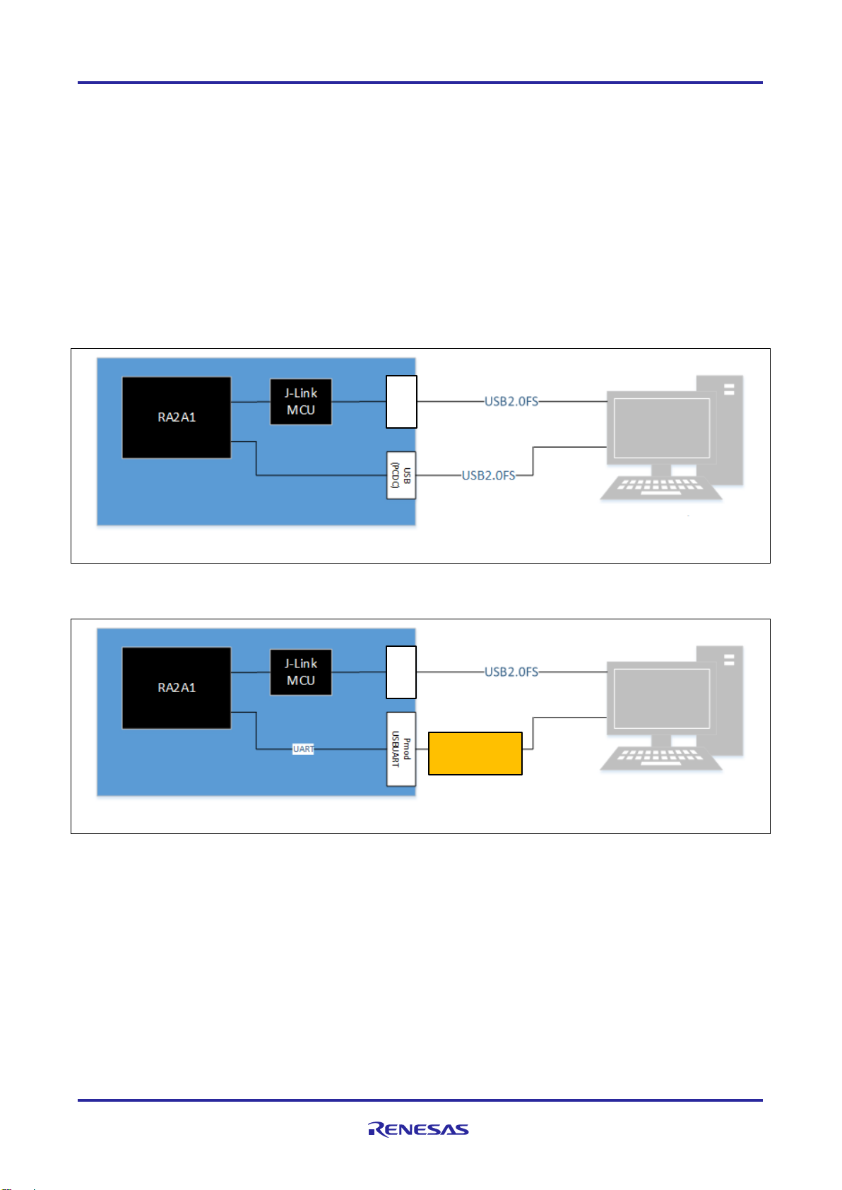
Figure 1-1 Connection Example for USB PCDC Communication
Figure 1-2 Connection Example for SCI UART Communication
QE for AFE
DEBUG
USB
UART
-USB
QE for AFE
DEBUG
USB
Page 4
RA2A1 Group Board Control Program for QE for AFE
R01AN5795EJ0100 Rev.1.00 Page 4 of 24
Mar.31.21
1.2 Operation Confirmation Environment
This FW is checked under the operating conditions shown in Table 1-1.
Table 1-1 Operating Confirmation Conditions
Items
Descriptions
MCU
(When using USB PCDC)
Clock-related Registers
SCKDIVCR = 0x10000101
SCKSCR = 0x00 (HOCO)
SDADCCKCR = 0x81
R7FA2A1AB3CFM (Renesas RA2A1 MCU Group)
Supply voltage: 3.3V
HOCO :48MHz
ICLK: 24MHz
PCLKB: 24MHz
PCLKD: 24MHz (used for ADC16)
FCLK: 24MHz
SDADCCLK: HOCO 48MHz
UCLK: 48MHz
MCU
(When using SCI UART)
Clock-related Registers
SCKDIVCR = 0x11000101
SCKSCR = 0x00 (HOCO)
SDADCCKCR = 0x81
R7FA2A1AB3CFM (Renesas RA2A1 MCU Group)
Supply voltage: 3.3V
HOCO: 64MHz
ICLK: 32MHz
PCLKB: 32MHz
PCLKD: 32MHz (used for ADC16)
FCLK: 32MHz
SDADCCLK: HOCO 64MHz
IDE
Renesas e2 studio V2021-01 (21.1.0)
FSP
Use v1.20 (not included in the IDE above)
Tool Chain
GNU ARM Embedded 9.2.1.20191025
Emulator
SEGGER J-Link®
USB-UART Adapter
PmodTM USBUART
Page 5

RA2A1 Group Board Control Program for QE for AFE
R01AN5795EJ0100 Rev.1.00 Page 5 of 24
Mar.31.21
1.3 File Configurations
The following is a list of file configurations. The description of some folders and files is omitted.
r01an5795xx0100-ra2a1-serial
├─ek_ra2a1
│ ├─QE_for_AFE_uart e2 studio project for QE_for_AFE_uart (SCI UART Communication)
│ │ ├─.settings
│ │ ├─ra
│ │ ├─ra_cfg
│ │ ├─ra_gen
│ │ ├─script
│ │ └─src
│ │ ├─hal_entry.c
│ │ ├─hal_entry.h
│ │ ├─r_common_config.h
│ │ ├─r_common_func.c
│ │ ├─r_common_func_if.h
│ │ ├─r_communication_control_api.c
│ │ ├─r_communication_control_api_if.h
│ │ ├─r_interrupt_callback.c
│ │ ├─r_interrupt_callback_if.h
│ │ ├─r_reg_chk.c
│ │ ├─r_reg_chk_if.h
│ │ ├─r_ring_buffer_control_api.c
│ │ ├─r_ring_buffer_control_api_if.h
│ │ └─r_usb_pcdc_descriptor.c
│ └─QE_for_AFE_usb e2 studio project for QE_for_AFE_uart (USB PCDC Communication)
│ ├─.settings
│ ├─ra
│ ├─ra_cfg
│ ├─ra_gen
│ ├─script
│ └─src
│ ├─hal_entry.c
│ ├─hal_entry.h
│ ├─r_common_config.h
│ ├─r_common_func.c
│ ├─r_common_func_if.h
│ ├─r_communication_control_api.c
│ ├─r_communication_control_api_if.h
│ ├─r_interrupt_callback.c
│ ├─r_interrupt_callback_if.h
│ ├─r_reg_chk.c
│ ├─r_reg_chk_if.h
│ ├─r_ring_buffer_control_api.c
│ ├─r_ring_buffer_control_api_if.h
│ └─r_usb_pcdc_descriptor.c
├─Hex
│ ├─QE_for_AFE_uart.hex Hex file for USB PCDC Communication (QE_for_AFE_uart)
│ └─QE_for_AFE_usb.hex Hex file for SCI UART Communication (QE_for_AFE_usb)
├─qe4qfe_setting
│ └─qe4afe_sample.2a1 Samle congiguration file for QE_for_AFE
├─r01an5795ej0100-ra2a1-serial.pdf
└─r01an5795jj0100-ra2a1-serial.pdf
Figure 1-3 File Configurations
Page 6
RA2A1 Group Board Control Program for QE for AFE
R01AN5795EJ0100 Rev.1.00 Page 6 of 24
Mar.31.21
1.4 Peripherals to Use
The following shows the list of peripherals used in this FW, and the settings for each peripheral function are
shown below.
Table 1-2 Peripheral Features List
Project
Intended Use
SDADC24
A/D measurement
ADC16
A/D measurement
DAC12
D/A output (output function from pin is not supported)
DAC8
D/A output (output function from pins is not supported)
OPAMP
Amplification of analog input voltage
USB FS [Note 1]
Communication: Used of PCDC
SCI0 [Note 1]
Communication: Used of UART communication: Use the PMOD B connector
DTC
Used for SCI0 UART communication
AGT0/1
Reservations (currently unused)
Note 1: Select either USB PCDC or SCI0 UART as communication I/F.
Page 7
RA2A1 Group Board Control Program for QE for AFE
R01AN5795EJ0100 Rev.1.00 Page 7 of 24
Mar.31.21
1.5 Pin Settings
1.5.1 Pin List
The following is a list of pins used in this FW.
Table 1-3 Pins used List
No
Pin
Configuration Function
Content
1
P400
CMPIN0
Used as an analog pin [Note 2]
2
P401
P401
RTS Pin Assignment for SCI0 UART (L
Fixed)
3
P402
P402
- 4 P403
P403
- 5 VCL
VCL
- 6 P215
XCIN
- 7 P214
XCOUT
- 8 VSS
VSS
- 9 P213
XTAL
-
10
P212
EXTAL
-
11
VCC
XCOUT
-
12
P411
P411
TXD0 pin for SCI0 UART
13
P410
P410
14
P409
P409
-
15
P408
CMPIN1
Used as an analog pin [Note 2]
16
P407
USB_VBUS
USB FS VBUS
17
VSS_USB
VSS_USB
-
18
P915
USB_DM
D- I/O pin for on-chip USB transceiver
19
P914
USB_DP
D+ I/O pin for on-chip USB transceiver
20
VCC_USB
VCC_USB
-
21
VCC_USB_LDO
VCC_USB_LDO
-
22
P206
P206
-
23
P205
P205
For LED1 control
24
P204
P204
RXD0 pin for SCI0 UART
25
Nothing
Nothing
-
26
P201
MD - 27
P200
P200
-
28
P304
P304
-
29
P303
P303
-
30
P302
P302
-
31
P301
P301
-
32
P300
SWCLK
-
33
P108
SWDIO
-
34
P110
CMPREF1
Reference voltage input pin [Note 2]
35
P111
P111
-
36
P112
P112
-
37
ADREG
ADREG
-
38
SBIAS/VREFI
SBIAS/VREF1
-
39
AVCC1
AVCC1
-
40
AVSS1
AVSS1
-
41
P107
ANSD3N/AN023
Used as an analog pin
42
P106
ANDS3P/AN022
Used as an analog pin
43
P105
ANSD2N/AN021
Used as an analog pin
44
P104
ANDS2P/AN020
Used as an analog pin
Page 8
RA2A1 Group Board Control Program for QE for AFE
R01AN5795EJ0100 Rev.1.00 Page 8 of 24
Mar.31.21
45
P103
ANSD1N/AN019
Used as an analog pin
46
P102
ANDS1P/AN018
Used as an analog pin
47
P101
ANSD0N/AN017/IVREF2
Used as an analog pin
48
P100
ANDS0P/AN016/IVCMP2
Used as an analog pin
49
P500
AN000/IVCMP0/AMP0+/DA12_0
Used as an analog pin [Note 1]
50
P501
AN001/IVREF0/AMP0-
Used as an analog pin
51
P502
AN002/AMP0O
Used as an analog pin
52
P015
AN003/AMP1O
Used as an analog pin
53
P014
AN004/IVREF1/AMP1-
Used as an analog pin
54
P013
AN005/IVCMP1/AMP1+/DA8_0
Used as an analog pin [Note 1]
55
P012
AN008/AMP2O
Used as an analog pin
56
AVCC0
AVCC0
-
57
AVSS0
AVSS0
58
VREFL0
VREFL0
ADC16 reference power supply (Low
potential reference voltage)
59
VREFH0
VREFH0
ADC16 reference power supply (High
potential reference voltage)
60
P003
AN006/AMP2-
Used as an analog pin
61
P002
AN007/AMP2+/DA8_1
Used as an analog pin [Note 1]
62
P001
P001
-
63
P000
P000
-
64
P109
CMPREF0
Reference voltage input pin [Note 2]
Note 1: It cannot be used as a D/A output pin.
Note 2: It is for ACMPHS/ACMPLP and cannot be used.
1.5.2 ADC16 Precautions When Using
The reference power supply pin (VREFH0) or internal reference voltage for the ADC16 (VREFADC) is
selectable as the high potential reference voltage. The low potential reference voltage is the reference
power supply ground pin (VRVEFL0).
On the EK-RA2A1 board, the VREFH0 and VREFL0 are open. Therefore, the VREFL0 must be set when
using ADC16.
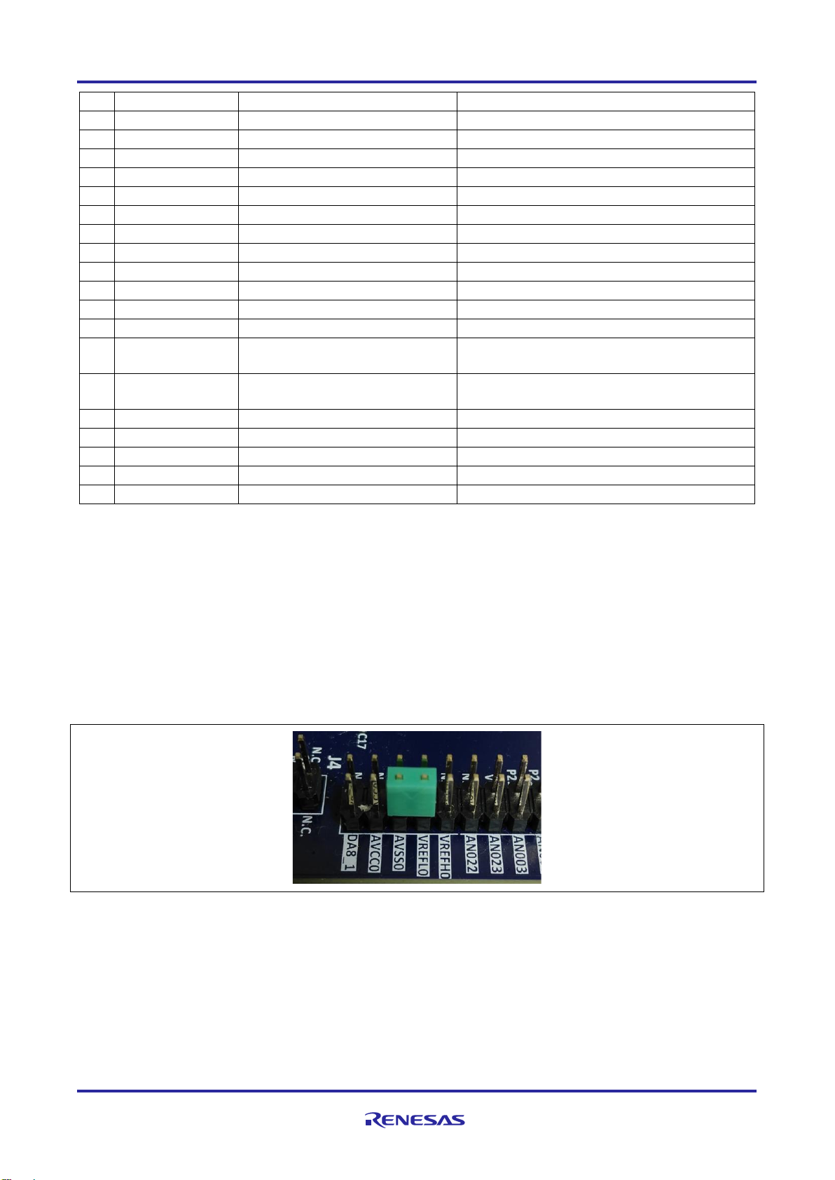
When connecting to AVSS0, connect to J2 34 pin (VREFL0) and J2 36 pin (AVSS0) on EK-RA2A1 board.
Because they are pins next to each other, it can be easily connected using a jumper as shown below.
Figure 1-4 Connecting J2 34-pin (VREFL0) and J2 36-pin (AVSS0) on Board Using ADC16
1.5.3 How LED1 Work
The LED1 on the EK-RA2A1 board lights up during A/D conversion operation on the SDADC24 or ADC16.
By opening the copper jumper E3 on the EK-RA2A1 board, LED lighting can be suppressed. For more
information, refer to ‘5.4.4 LEDs’ in the ‘EK-RA2A1 v1 User Manual (R20UT4580EU0101)’.
Page 9

RA2A1 Group Board Control Program for QE for AFE
R01AN5795EJ0100 Rev.1.00 Page 9 of 24
Mar.31.21
1.6 Communication Specifications
The communication specifications for ‘QE for AFE’ and FW are as follows.
1.6.1 Serial Communication Settings
The serial communication settings for UART communication are as follows:
Table 1-4 Serial Communication Settings
Items
Settings
Transfer Speed
Default: 1M bps
Maximum: 3M bps [Note 1]
Data Length
8-bit
Parity
No parity
Stop Bit
1-bit
Hardware Flow Control
CTS function disabled (RTS function enabled)
Assigned the RTS pin to the P401 and L-fixed is output
Note 1: Depends on the specifications of the USB-UART adapter that connects to the PMOD B connector on
the EK-RA2A1 board. Therefore, 3M bps may not be supported.
1.6.2 Connecting USB-UART adapter during UART communication
Connect the USB-UART adapter to the PMOD B connector on the EK-RA2A1 board.
For information about the USB-UART adapter used to confirmed operation, refer to ‘1.2 Operation
Confirmation Environment’.
1.7 About Project Source Changes
Do not change any settings other than the clock settings in FSP Configuration.
1.8 Related Documentation
• Renesas RA2A1 Group User's Manual: Hardware (R01UH0888EJ0100)
• Renesas RA2A1 Group Evaluation Kit for RA2A1 Microcontroller Group EK-RA2A1 Quick Start Guide
(R20QS0010EU0102)
• Renesas RA2A1 Group Evaluation Kit for RA2A1 Microcontroller Group EK-RA2A1 v1 User's Manual
(R20UT4580EU0101)
Page 10

RA2A1 Group Board Control Program for QE for AFE
R01AN5795EJ0100 Rev.1.00 Page 10 of 24
Mar.31.21
2. How to Write FW
The method of writing FW to the EK-RA2A1 board is shown below.
2.1 Write Using e2 studio Integrated Development Environment (IDE)
Import the project, build the project, and write to RA2A1 on the EK-RA2A1 board. The following projects are
included.
Table 2-1 e2 studio Project
Project Name
Folder Name
USB PCDC Communication Project
QE_for_AFE_usb.hex
SCI UART Communication Project
QE_for_AFE_uart.hex
2.1.1 Import Procedure
The import procedure is shown in the figure below.
Figure 2-1 Steps to Import a Project into e2 studio
2.1.2 Notes on Building Project for USB PCDC Communication
Two Warnings occur during build. Ignore it because it is used by a program for unused functions.
Figure 2-2 Project Build Results for USB PCDC Communication Project
Select ’Import’.
Select ’Existing Project into
Workspace’.
Select the directory where
the project is stored.
Page 11

RA2A1 Group Board Control Program for QE for AFE
R01AN5795EJ0100 Rev.1.00 Page 11 of 24
Mar.31.21
2.1.3 Notes on Building Project for SCI UART Communication
After import, the warning occurs as follows. This indicates an error for USB clock configuration. The SCI
UART communication project does not use USB I/F. Therefore, ignore it.
Figure 2-3 Warning in FSP Configuration for SCI UART Communication Project
Also, two warnings occur during build. Ignore it because it is used by a program for unused functions.
Figure 2-4 Project Build Results for SCI UART Communication Project
Page 12

RA2A1 Group Board Control Program for QE for AFE
R01AN5795EJ0100 Rev.1.00 Page 12 of 24
Mar.31.21
2.2 Writing using Renesas Flash Programmer
You can write HEX files to the RA2A1 on the EK-RA2A1 board using Renesas Flash Programmer. The
following HEX files are included.
Table 2-2 HEX Files
HEX Files
File Name
HEX File for USB PCDC Communication
QE_for_AFE_usb.hex
HEX File for SCI UART Communication
QE_for_AFE_uart.hex
Get the Renesas Flash Programmer that supports RA Family from the following.
Renesas Flash Programmer (Programming GUI) | Renesas
The following is the explanation when using Renesas Flash Programmer V3.08.01.
Also, make the Renesas Flash Programmer aware of the EK-RA2A1 board. The procedure is shown below:
(1) Switch J8 Jumper on EK-RA2A1 Board
Switch the J8 jumper to ‘SCI/USB BOOT’.
Figure 2-5 Setting J8 Jumper to ‘SCI/USB BOOT’ (Set When Writing FW)
(2) Connect PC to EK-RA2A1 Board
Connect both DEBUG USB and DEVICE USB to your PC.
At this point, the PC device manager recognizes the EK-RA2A1 board as USB Serial Device.
(3) Press RESET Button
Press the RESET button. The PC device manager recognizes the EK-RA2A1 board as ‘RA USB
Boot(CDC)’.
Figure 2-6 RESET Button
Page 13

RA2A1 Group Board Control Program for QE for AFE
R01AN5795EJ0100 Rev.1.00 Page 13 of 24
Mar.31.21
(4) Launch the Renesas Flash Programmer
(a) If No Project for RA Family Has Been Created
Create a new project.
Set the ‘Microcontroller’ in ‘Project Information’ to “RA”.
Set the ‘Tool’ of ‘Communication’ to "COM port".
Figure 2-7 Setting of ‘Microcontroller’ and ‘Tool’
Click ‘Tool Details…’ in ‘Communication’ and select "RA USB Boot(CDC)" on the ‘Select Tool’ tab. After
confirming, click "OK".
If you see USB Serial Device, check the J8 jumper setting and press RESET button again.
Figure 2-8 "RA USB Boot(CDC)" Selected
Return to the ‘Create New Project Window’ and click “Connect”. Renesas Flash Programmer starts the
connection process.
Page 14

RA2A1 Group Board Control Program for QE for AFE
R01AN5795EJ0100 Rev.1.00 Page 14 of 24
Mar.31.21
(b) If Project for RA Family Has Been Created
Open the project.
Click on the ‘Connect Settings’ tab.
Figure 2-9 Setting of ‘Connect Setting’ Tab
Set the ‘Tool’ of ‘Communication’ to "COM port". Refer to also ‘Figure 2-7 Setting of ‘Microcontroller’ and
‘Tool’ ’.
Click ‘Tool Details’ in ‘Communication’ and select "RA USB Boot(CDC)" on the ‘Select Tool’ tab. Refer to
also ‘Figure 2-8 "RA USB Boot(CDC)" Selected’. After confirming, click "OK".
If you see USB Serial Device, check the J8 jumper setting and press RESET button again.
(5) Follow Instructions in Renesas Flash Programmer to Write FW
Note: After the write is complete, be sure to return the J8 jumper to its original state and press the RESET
button.
Figure 2-10 Set J8 Jumper to ‘INTERNAL FLASH’ (Return to Original Setting after Writing)
Page 15

RA2A1 Group Board Control Program for QE for AFE
R01AN5795EJ0100 Rev.1.00 Page 15 of 24
Mar.31.21
3. Run Project
3.1 Connecting to PC
Debug USB I/F provides a power supply voltage for the EK-RA2A1 board. Refer to the ‘EK-RA2A1 v1 User's
Manual (R20UT4580EU0101)’.
Connection examples are shown below.
3.1.1 USB PCDC Communication
Figure 3-1 Connection Example for USB PCDC Communication
3.1.2 USB PCDC Communication
Turn on the power with the connection described in the EK-RA2A1 board manual.
Some USB-UART adapters can supply 3.3V voltage from the adapter. Do not use the function. This is
because the EK-RA2A1 board is powered from two different power sources.
Figure 3-2 Connection Example for SCI UART Communication
QE for AFE
DEBUG
USB
UART
-USB
QE for AFE
DEBUG
USB
Page 16

RA2A1 Group Board Control Program for QE for AFE
R01AN5795EJ0100 Rev.1.00 Page 16 of 24
Mar.31.21
3.2 Launch QE for AFE
Launch ‘QE for AFE’ and evaluate it according to the operating procedure.
For details on the operation of ‘QE for AFE’, refer to the ‘QE for AFE’ manual.
3.2.1 Preparation
Prepare the following in advance.
(1) Connection J2 34 Pin (VREFL0) and J2 36 Pin (AVSS0) on EK-RA2A1 Board
Refer to ‘1.5.2 ADC16 Precautions When Using’.
(2) Writing FW
Refer to ‘2 How to Write FW’.
Also, when writing using Renesas Flash Programmer, make sure that the J8 jumper is set to ‘INTERNAL
FLASH’. Otherwise, you will not be able to get the correct A/D value.
(3) Connection between PC and EK-RA2A1 Board
Refer to ‘3.1 Connecting to PC’.
3.2.2 Launching QE for AFE and Connecting to Target Board
Follow the steps below to connect the target board.
(1) Launching QE for AFE
(2) Connection with Target Board
Check the COM number of USB Serial Device in the PC device manager and select the COM number from
‘COM Port:’.
Figure 3-3 Selecting COM Number
Also, check the following display on the console.
[Info]Connect succeed.
Figure 3-4 Message on Console when Connection is Successful
3.2.3 Operation Confirmation
You can check the operation using the included sample setting file.
For the contents of the sample configuration file, refer to ‘3.3 Sample Configuration File’.
For the operation method using the sample setting file, refer to ‘3.4 QE for AFE Tuning Execution’.
Page 17

RA2A1 Group Board Control Program for QE for AFE
R01AN5795EJ0100 Rev.1.00 Page 17 of 24
Mar.31.21
3.3 Sample Configuration File
The sample configuration file for ‘QE for AFE’ that has been confirmed to work has been stored.
You can easily confirm the operation by importing the sample configuration file.
Table 3-1 Sample Configuration Files for Operation Confirmation
Settings File
File Name
Sample configuration file
qe4afe_sample.2a1
Click the icon below and select the import file above.
Figure 3-5 Icon for ‘Import setting file’
The file is selected, the "Register setting file" window is displayed.
The sample configuration file contains the settings for "SDADC24", "ADC16", "OPAMP", "DAC8", and
"DAC12".
Figure 3-6 ‘Register setting file’ Window
Page 18

RA2A1 Group Board Control Program for QE for AFE
R01AN5795EJ0100 Rev.1.00 Page 18 of 24
Mar.31.21
3.3.1 Configuration Overview of Sample Configuration File
The overview of the settings in the sample configuration file is shown below.
(1) OPAMP Settings
Table 3-2 OPAMP Settings
AMP
Configuration Overview
AMP0 Operation Enabled
+: DAC12 output is connected to AMP0+ input
-: Voltage follower setting
AMP1 Operation Enabled
+: DA8_0 output is connected to AMP1+ input
-: Voltage follower setting
AMP2 Operation Enabled
+: DA8_1 output is connected to AMP2+ input
-: Voltage follower setting
(2) DAC12 Settings
Table 3-3 DAC12 Settings
DAC12
Configuration Overview
DAC12 Operation Enabled
Output 1.0 V
(It is possible to change the output voltage by changing DADR register.)
(3) DAC8 Settings
Table 3-4 DAC8 Settings
DAC8
Configuration Overview
DAC8_0 Operation Enabled
Output 0.5 V
(It is possible to change the output voltage by changing DACS0 register.)
DAC8_1 Operation Enabled
Output 1.5V
(It is possible to change the output voltage by changing DACS1 register.)
(4) SDADC24 Settings
Table 3-5 SDADC24 Settings
SDADC24
Configuration Overview
A/D Conversion Mode
Normal A/D conversion mode
Ch4 only Operation Enabled
Ch4: DAC12 output voltage can be A/D conversion.
PGA Settings (All Ch)
Gain=1, OSR=256, Single end setting, ‘Do not average the A/D
conversion results’ setting
(5) ADC16 Settings
Table 3-6 ADC16 Settings
ADC16
Configuration Overview
VREFH0
VREFADC= 2.5V
Ch Settings
Only Ch2, Ch3, Ch8
Operation Enabled
Ch2: DAC12 output voltage can be A/D converted
Ch3: DAC8_0 output voltage can be A/D converted
Ch8: DAC8_1 output voltage can be A/D converted
Input mode
Single end setting
Single Ended Input A/D
Conversion Data Inversion
(ADCER)
Single ended A/D converted data of single ended mode for odd-channels
inputs: ‘Data is stored in a range from 0 to 32767.’
Page 19

RA2A1 Group Board Control Program for QE for AFE
R01AN5795EJ0100 Rev.1.00 Page 19 of 24
Mar.31.21
3.3.2 Setting Procedure after Import
After importing, it is necessary to correct the setting values. The procedure for each project is shown below.
3.3.2.1 Project for USB PCDC Communication
(1) Clock Setting
After importing the file, set the clock first.
In the sample setting file, it is possible to acquire A / D of both SDADC24 and ADC16, so set both.
(a) SDADC24 Setting
Re-enter both places as shown below. By re-entering the setting value, the setting value is checked.
Figure 3-7 Clock Settings for SDADC24 during USB PCDC Communication (For HOCO 48MHz)
(b) ADC16 Setting
Re-enter both places as shown below. By re-entering the setting value, the setting value is checked.
Figure 3-8 Clock Settings for ADC16 during USB PCDC Communication (For HOCO 48MHz)
(2) Setting of ADC16 A/D Sampling State Register n (ADSSTRn)
Set "10.625" for all channels to be used as follows so that the value of ADSSTRn is 0xFF.
A/D scan end interrupt occurs during interrupt processing and A/D scan does not operate normally.
Therefore, it is necessary to set the ADSSTRn and adjust the sampling time.
Figure 3-9 Settings for ADC16 ADSSTRn during USB PCDC Communication
Page 20

RA2A1 Group Board Control Program for QE for AFE
R01AN5795EJ0100 Rev.1.00 Page 20 of 24
Mar.31.21
3.3.2.2 Project for SCI UART Communication
(1) Clock Setting
After importing the file, set the clock first.
In the sample setting file, it is possible to acquire A / D of both SDADC24 and ADC16, so set both.
(a) SDADC24 Setting
Re-enter both places as shown below. By re-entering the setting value, the setting value is checked.
Figure 3-10 Clock Settings for SDADC24 during SCI UART Communication (For HOCO 64MHz)
(b) ADC16 Setting
Re-enter both places as shown below. By re-entering the setting value, the setting value is checked.
Figure 3-11 Clock Settings for ADC16 during SCI UART Communication (For HOCO 64MHz)
(2) Setting of ADC16 A/D Sampling State Register n (ADSSTRn)
Set "7.96875" for all channels to be used as follows so that the value of ADSSTRn is 0xFF.
A/D scan end interrupt occurs during interrupt processing and A/D scan does not operate normally.
Therefore, it is necessary to set the ADSSTRn and adjust the sampling time.
Figure 3-12 Settings for ADC16 ADSSTRn during SCI UART Communication
Page 21

RA2A1 Group Board Control Program for QE for AFE
R01AN5795EJ0100 Rev.1.00 Page 21 of 24
Mar.31.21
3.4 QE for AFE Tuning Execution
3.4.1 Writing Setting Value
Write the setting value to the target board for all controlled tabs (in case of the sample configuration file,
‘SDADC24’, ‘ADC16’, ‘OPAMP’, ‘DAC8’, and ‘DAC12’ tabs) on ‘AFE Connection’.
Figure 3-13 Icon for ‘Write Value to the Target Board’
After importing the configuration file, write in all controlled tabs and check the following display on the
console.
If all controlled registers are not written. it is not possible to control correctly.
[Info]Write ‘IP Name’ register value to the target board successfully.
Figure 3-14 Message on Console when Writing is Successful
Page 22

RA2A1 Group Board Control Program for QE for AFE
R01AN5795EJ0100 Rev.1.00 Page 22 of 24
Mar.31.21
3.4.2 Tuning Operation
The capture screen at run time is shown below.
Click ‘AD Monitor’. Then, it will switch to the tuning screen.
Click the icon for ‘Start AFE Tuning’ to start A/D conversion.
Figure 3-15 Icon for ‘Start AFE Tuning’
(1) SDADC24
The A/D value acquisition screen for Ch4 is shown in the figure below. To obtain the A/D value for Ch4 only,
"Auto Scale" is set to disabled, and the Y axis is displayed in the maximum range.
If you want to change the output voltage of DAC12, stop tuning, change the DAC12 DADR register and write.
Pay attention to the input allow voltage (0.2 to1.8V) of the SDADC24 and set the output voltage of DAC12.
Figure 3-16 QE for AFE Operating Screen (SDADC24, DAC12 Output Voltage =1.0V)
Page 23

RA2A1 Group Board Control Program for QE for AFE
R01AN5795EJ0100 Rev.1.00 Page 23 of 24
Mar.31.21
(2) ADC16
The A/D value acquisition screen for Ch2, Ch3, and Ch8 is shown in the figure below.
Since the measured voltage is 0.5V to 1.5V, it is displayed by enabling "Autoscale". If necessary, you can
disable "Autoscale" to zoom in/out.
If you want to change the output voltages of DAC12 and DAC8, stop tuning, change theDAC12 DADR
register, DAC8n DACSn registers, and write.
In this setting, the reference power supply VREFH0 is 2.5V for ADC16. Carefully set the output voltage of
DAC12 and DAC8.
Figure 3-17 QE for AFE Operating Screen (ADC16, DAC12 output voltage = 1.0V, DAC8_0 output
voltage = 0.5V, DAC8_1 output voltage= 1.5V)
Page 24

RA2A1 Group Board Control Program for QE for AFE
R01AN5795EJ0100 Rev.1.00 Page 24 of 24
Mar.31.21
Revision History
Rev.
Date
Description
Page
Summary
1.00
Mar.31.21
-
First Release
Page 25

General Precautions in the Handling of Microprocessing Unit and Microcontroller Unit Products
The following usage notes are applicable to all Microprocessing unit and Microcontroller unit products from Renesas. For detailed usage notes on the
products covered by this document, refer to the relevant sections of the document as well as any technical updates that have been issued for the products.
1. Precaution against Electrostatic Discharge (ESD)
A strong electrical field, when exposed to a CMOS device, can cause destruction of the gate oxide and ultimately degrade the device operation. Steps
must be taken to stop the generation of static electricity as much as possible, and quickly dissipate it when it occurs. Environmental control must be
adequate. When it is dry, a humidifier should be used. This is recommended to avoid using insulators that can easily build up static electricity.
Semiconductor devices must be stored and transported in an anti-static container, static shielding bag or conductive material. All test and
measurement tools including work benches and floors must be grounded. The operator must also be grounded using a wrist strap. Semiconductor
devices must not be touched with bare hands. Similar precautions must be taken for printed circuit boards with mounted semiconductor devices.
2. Processing at power-on
The state of the product is undefined at the time when power is supplied. The states of internal circuits in the LSI are indeterminate and the states of
register settings and pins are undefined at the time when power is supplied. In a finished product where the reset signal is applied to the external reset
pin, the states of pins are not guaranteed from the time when power is supplied until the reset process is completed. In a similar way, the states of pins
in a product that is reset by an on-chip power-on reset function are not guaranteed from the time when power is supplied until the power reaches the
level at which resetting is specified.
3. Input of signal during power-off state
Do not input signals or an I/O pull-up power supply while the device is powered off. The current injection that results from input of such a signal or I/O
pull-up power supply may cause malfunction and the abnormal current that passes in the device at this time may cause degradation of internal
elements. Follow the guideline for input signal during power-off state as described in your product documentation.
4. Handling of unused pins
Handle unused pins in accordance with the directions given under handling of unused pins in the manual. The input pins of CMOS products are
generally in the high-impedance state. In operation with an unused pin in the open-circuit state, extra electromagnetic noise is induced in the vicinity of
the LSI, an associated shoot-through current flows internally, and malfunctions occur due to the false recognition of the pin state as an input signal
become possible.
5. Clock signals
After applying a reset, only release the reset line after the operating clock signal becomes stable. When switching the clock signal during program
execution, wait until the target clock signal is stabilized. When the clock signal is generated with an external resonator or from an external oscillator
during a reset, ensure that the reset line is only released after full stabilization of the clock signal. Additionally, when switching to a clock signal
produced with an external resonator or by an external oscillator while program execution is in progress, wait until the target clock signal is stable.
6. Voltage application waveform at input pin
Waveform distortion due to input noise or a reflected wave may cause malfunction. If the input of the CMOS device stays in the area between VIL
(Max.) and VIH (Min.) due to noise, for example, the device may malfunction. Take care to prevent chattering noise from entering the device when the
input level is fixed, and also in the transition period when the input level passes through the area between VIL (Max.) and VIH (Min.).
7. Prohibition of access to reserved addresses
Access to reserved addresses is prohibited. The reserved addresses are provided for possible future expansion of functions. Do not access these
addresses as the correct operation of the LSI is not guaranteed.
8. Differences between products
Before changing from one product to another, for example to a product with a different part number, confirm that the change will not lead to problems.
The characteristics of a microprocessing unit or microcontroller unit products in the same group but having a different part number might differ in terms
of internal memory capacity, layout pattern, and other factors, which can affect the ranges of electrical characteristics, such as characteristic values,
operating margins, immunity to noise, and amount of radiated noise. When changing to a product with a different part number, implement a systemevaluation test for the given product.
Page 26

© 2021 Renesas Electronics Corporation. All rights reserved.
Notice
1. Descriptions of circuits, software and other related information in this document are provided only to illustrate the operation of semiconductor products
and application examples. You are fully responsible for the incorporation or any other use of the circuits, software, and information in the design of your
product or system. Renesas Electronics disclaims any and all liability for any losses and damages incurred by you or third parties arising from the use
of these circuits, software, or information.
2. Renesas Electronics hereby expressly disclaims any warranties against and liability for infringement or any other claims involving patents, copyrights,
or other intellectual property rights of third parties, by or arising from the use of Renesas Electronics products or technical information described in this
document, including but not limited to, the product data, drawings, charts, programs, algorithms, and application examples.
3. No license, express, implied or otherwise, is granted hereby under any patents, copyrights or other intellectual property rights of Renesas Electronics
or others.
4. You shall not alter, modify, copy, or reverse engineer any Renesas Electronics product, whether in whole or in part. Renesas Electronics disclaims any
and all liability for any losses or damages incurred by you or third parties arising from such alteration, modification, copying or reverse engineering.
5. Renesas Electronics products are classified according to the following two quality grades: “Standard” and “High Quality”. The intended applications for
each Renesas Electronics product depends on the product’s quality grade, as indicated below.
"Standard": Computers; office equipment; communications equipment; test and measurement equipment; audio and visual equipment; home
electronic appliances; machine tools; personal electronic equipment; industrial robots; etc.
"High Quality": Transportation equipment (automobiles, trains, ships, etc.); traffic control (traffic lights); large-scale communication equipment; key
financial terminal systems; safety control equipment; etc.
Unless expressly designated as a high reliability product or a product for harsh environments in a Renesas Electronics data sheet or other Renesas
Electronics document, Renesas Electronics products are not intended or authorized for use in products or systems that may pose a direct threat to
human life or bodily injury (artificial life support devices or systems; surgical implantations; etc.), or may cause serious property damage (space
system; undersea repeaters; nuclear power control systems; aircraft control systems; key plant systems; military equipment; etc.). Renesas Electronics
disclaims any and all liability for any damages or losses incurred by you or any third parties arising from the use of any Renesas Electronics product
that is inconsistent with any Renesas Electronics data sheet, user’s manual or other Renesas Electronics document.
6. When using Renesas Electronics products, refer to the latest product information (data sheets, user’s manuals, application notes, “General Notes for
Handling and Using Semiconductor Devices” in the reliability handbook, etc.), and ensure that usage conditions are within the ranges specified by
Renesas Electronics with respect to maximum ratings, operating power supply voltage range, heat dissipation characteristics, installation, etc. Renesas
Electronics disclaims any and all liability for any malfunctions, failure or accident arising out of the use of Renesas Electronics products outside of such
specified ranges.
7. Although Renesas Electronics endeavors to improve the quality and reliability of Renesas Electronics products, semiconductor products have specific
characteristics, such as the occurrence of failure at a certain rate and malfunctions under certain use conditions. Unless designated as a high reliability
product or a product for harsh environments in a Renesas Electronics data sheet or other Renesas Electronics document, Renesas Electronics
products are not subject to radiation resistance design. You are responsible for implementing safety measures to guard against the possibility of bodily
injury, injury or damage caused by fire, and/or danger to the public in the event of a failure or malfunction of Renesas Electronics products, such as
safety design for hardware and software, including but not limited to redundancy, fire control and malfunction prevention, appropriate treatment for
aging degradation or any other appropriate measures. Because the evaluation of microcomputer software alone is very difficult and impractical, you are
responsible for evaluating the safety of the final products or systems manufactured by you.
8. Please contact a Renesas Electronics sales office for details as to environmental matters such as the environmental compatibility of each Renesas
Electronics product. You are responsible for carefully and sufficiently investigating applicable laws and regulations that regulate the inclusion or use of
controlled substances, including without limitation, the EU RoHS Directive, and using Renesas Electronics products in compliance with all these
applicable laws and regulations. Renesas Electronics disclaims any and all liability for damages or losses occurring as a result of your noncompliance
with applicable laws and regulations.
9. Renesas Electronics products and technologies shall not be used for or incorporated into any products or systems whose manufacture, use, or sale is
prohibited under any applicable domestic or foreign laws or regulations. You shall comply with any applicable export control laws and regulations
promulgated and administered by the governments of any countries asserting jurisdiction over the parties or transactions.
10. It is the responsibility of the buyer or distributor of Renesas Electronics products, or any other party who distributes, disposes of, or otherwise sells or
transfers the product to a third party, to notify such third party in advance of the contents and conditions set forth in this document.
11. This document shall not be reprinted, reproduced or duplicated in any form, in whole or in part, without prior written consent of Renesas Electronics.
12. Please contact a Renesas Electronics sales office if you have any questions regarding the information contained in this document or Renesas
Electronics products.
(Note1) “Renesas Electronics” as used in this document means Renesas Electronics Corporation and also includes its directly or indirectly controlled
subsidiaries.
(Note2) “Renesas Electronics product(s)” means any product developed or manufactured by or for Renesas Electronics.
(Rev.4.0-1 November 2017)
Corporate Headquarters
Contact information
TOYOSU FORESIA, 3-2-24 Toyosu,
Koto-ku, Tokyo 135-0061, Japan
www.renesas.com
For further information on a product, technology, the most up-to-date
version of a document, or your nearest sales office, please visit:
www.renesas.com/contact/.
Trademarks
PmodTM is a trademark of Digilent Inc.
Renesas and the Renesas logo are trademarks of Renesas Electronics
Corporation. All trademarks and registered trademarks are the property
of their respective owners.
 Loading...