

Page 1

查询R8C2K供应商
PRELIMINARY
Notice: This is not a final specification.
Some parametric limits are subject to change.
R8C/2K Group, R8C/2L Group
REJ03B0219-0010
RENESAS MCU
1. Overview
1.1 Features
The R8C/2K Group and R8C/2L Group of single-chip MCUs incorporates the R8C/Tiny Series CPU core,
employing sophisticated instructions for a high level of efficiency. Wi th 1 Mbyte of address space and is capable of
executing instructions at high speed. In addition, the CPU core boasts a multiplier for high-speed operation
processing.
Power consumption is low, and the supported operating modes allow additional power control. These MCUs also
use an anti-noise configuration to reduce emissions of electromagnetic noise and are designed to withstand EMI.
Integration of many peripheral functions, including multifunction timer and serial interface, reduces the number of
system components.
Furthermore, the R8C/2L Group has on-chip data flash (1 KB × 2 blocks).
The difference between the R8C/2K Group and R8C/2L Group is only the presence or absence of data flash. Their
peripheral functions are the same.
1.1.1 Applications
Electronic household appliances, office equipment, audio equipment, consumer equipment, etc.
Rev.0.10
Jul 20, 2007
Rev.0.10 Jul 20, 2007 Page 1 of 44
REJ03B0219-0010
Page 2
Under development
Preliminary specification
Specications in this manual are tentative and subject to change
R8C/2K Group, R8C/2L Group 1. Overview
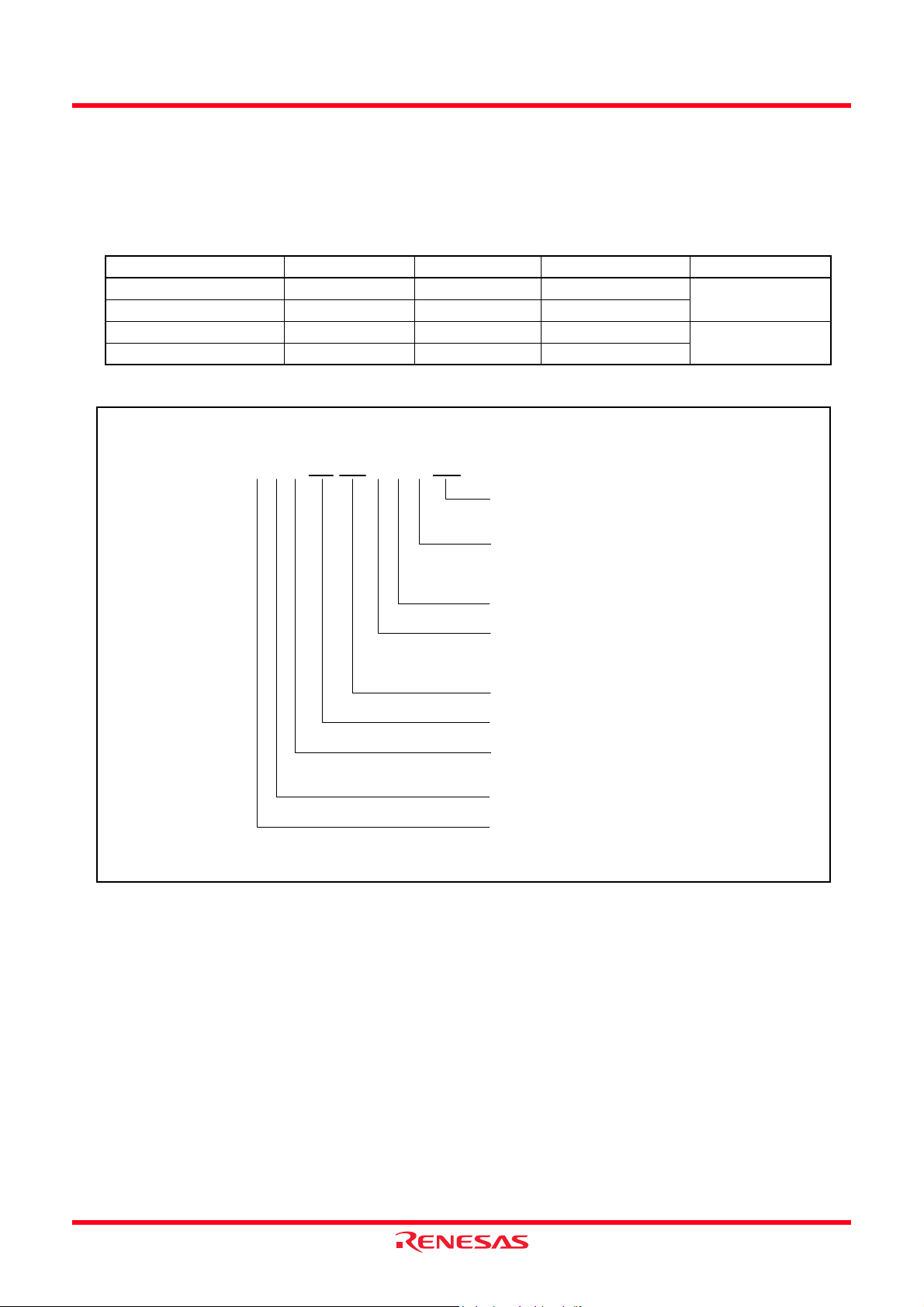
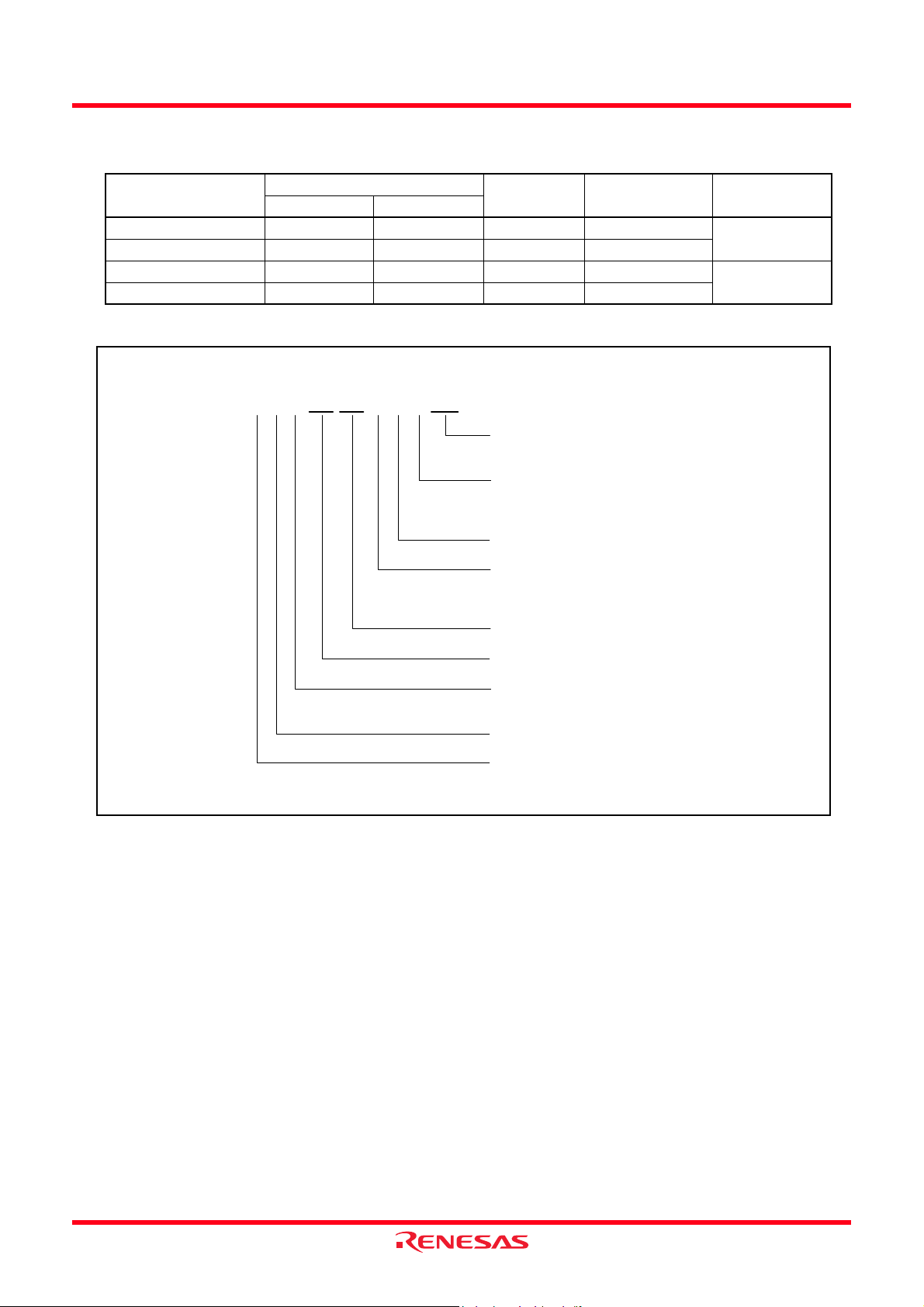
1.1.2 Specifications
Tables 1.1 and 1.2 outlines the Specifications for R8C/2K Group and Tables 1.3 and 1.4 outlines the
Specifications for R8C/2L Group
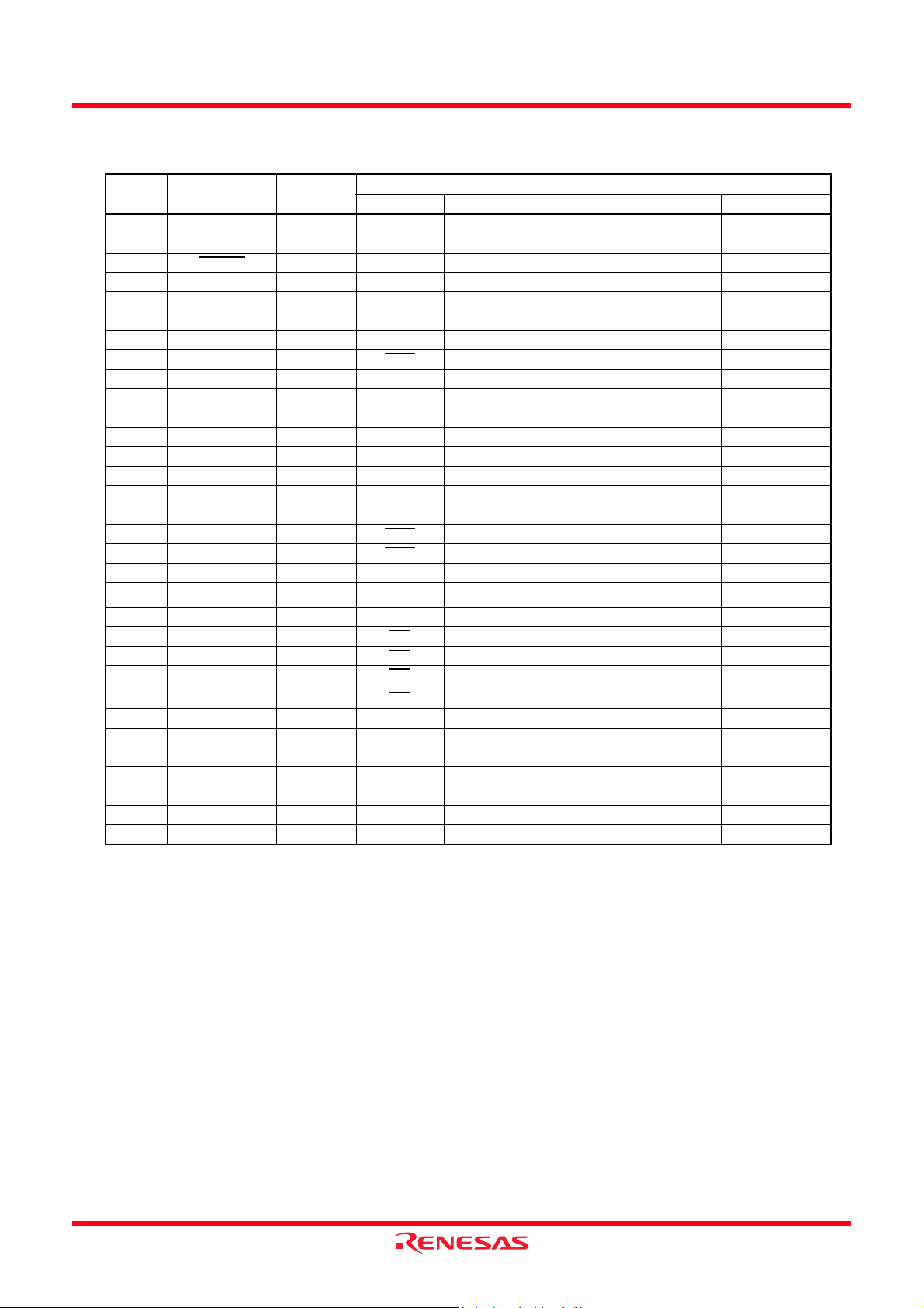
Table 1.1 Specifications for R8C/2K Group (1)
Item Function Specification
CPU Central processing
unit
Memory ROM, RAM Refer to T able 1.5 Product List for R8C/2K Group.
Power Supply
Voltage
Detection
I/O Ports Programmable I/O
Clock Clock generation
Interrupts • External: 4 sources, Internal: 15 sources, Software: 4 sources
Watchdog Timer 15 bits × 1 (with prescaler), reset start selectable
Timer Timer RA 8 bits × 1 (with 8-bit prescaler)
Voltage detection
circuit
ports
circuits
Timer RB 8 bits × 1 (with 8-bit prescaler)
Timer RC 16 bits × 1 (with 4 capture/compare registers)
Timer RD 16 bits × 2 (with 4 capture/compare registers)
R8C/Tiny series core
• Number of fundamental instructions: 89
• Minimum instruction execution time:
50 ns (f(XIN) = 20 MHz, VCC = 3.0 to 5.5 V)
100 ns (f(XIN) = 10 MHz, VCC = 2.7 to 5.5 V)
200 ns (f(XIN) = 5 MHz, VCC = 2.2 to 5.5 V)
• Multiplier: 16 bits × 16 bits → 32 bits
• Multiply-accumulate instruction: 16 bits × 16 bits + 32 bits → 32 bits
• Operation mode: Single-chip mode (address space: 1 Mbyte)
• Power-on reset
• Voltage detection 3
• Input-only: 3 pins
• CMOS I/O ports: 25, selectable pull-up resistor
• High current drive ports: 8
2 circuits: XIN clock oscillation circuit (with on-chip feedback resistor),
On-chip oscillator (high-speed, low-speed)
(high-speed on-chip oscillator has a frequency adjustment function)
• Oscillation stop detection: XIN clock oscillation stop detection function
• Frequency divider circuit: Dividing selectable 1, 2, 4, 8, and 16
• Low power consumption modes:
Standard operating mode (high-speed clock, high-speed on-chip oscillator,
low-speed on-chip oscillator), wait mode, stop mode
• Priority levels: 7 levels
Timer mode (period timer), pulse output mode (output level inverted every
period), event counter mode, pulse width measurement mode, pulse period
measurement mode
Timer mode (period timer), programmable waveform generation mode (PWM
output), programmable one-shot generation mode, programmable wait on eshot generation mode
Timer mode (input capture function, output compare function), PWM mode
(output 3 pins), PWM2 mode (PWM output pin)
Timer mode (input capture function, output compare function), PWM mode
(output 6 pins), reset synchronous PWM mode (output three-phase
waveforms (6 pins), sawtooth wave modulation), complementary PWM mode
(output three-phase waveforms (6 pins), triangular wave modulation), PWM3
mode (PWM output 2 pins with fixed period)
Rev.0.10 Jul 20, 2007 Page 2 of 44
REJ03B0219-0010
Page 3
Under development
Preliminary specification
Specications in this manual are tentative and subject to change
R8C/2K Group, R8C/2L Group 1. Overview
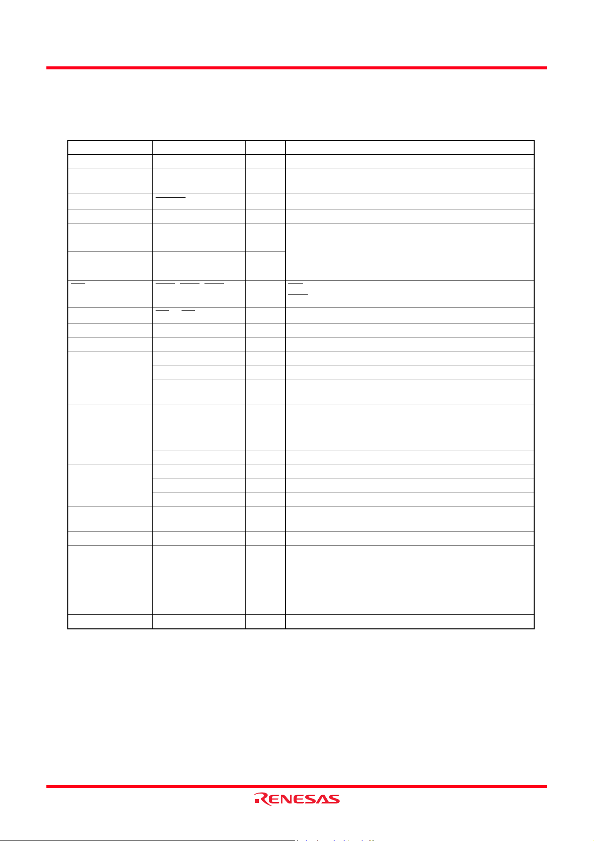
Table 1.2 Specifications for R8C/2K Group (2)
Item Function Specification
Serial
Interface
LIN Module Hardware LIN: 1 (timer RA, UART0)
A/D Converter 10-bit resolution × 9 channels, includes sample and hold function
Flash Memory • Programming and erasure voltage: VCC = 2.7 to 5.5 V
Operating Frequency/Supply
Voltage
Current consumption TBD (VCC = 5.0 V, f(XIN) = 20 MHz)
Operating Ambient Temperature -20 to 85°C (N version)
Package 32-pin LQFP
NOTE:
1. Specify the D version if D version functions are to be used.
UART0, UART2 Clock synchronous serial I/O/UART × 2
• Programming and erasure endurance: 100 times
• Program security: ROM code protect, ID code check
• Debug functions: On-chip debug, on-board flash rewrite function
f(XIN) = 20 MHz (VCC = 3.0 to 5.5 V)
f(XIN) = 10 MHz (VCC = 2.7 to 5.5 V)
f(XIN) = 5 MHz (VCC = 2.2 to 5.5 V) (VCC = 2.7 to 5.5 V for A/D converter only)
TBD (VCC = 3.0 V, f(XIN) = 10 MHz)
TBD (VCC = 3.0 V, wait mode)
TBD (VCC = 3.0 V, stop mode)
-40 to 85°C (D version)
(1)
• Package code: PLQP0032GB-A (previous code: 32P6U-A)
Rev.0.10 Jul 20, 2007 Page 3 of 44
REJ03B0219-0010
Page 4
Under development
Preliminary specification
Specications in this manual are tentative and subject to change
R8C/2K Group, R8C/2L Group 1. Overview
Table 1.3 Specifications for R8C/2L Group (1)
Item Function Specification
CPU Central processing
unit
Memory ROM, RAM Refer to T able 1.6 Product List for R8C/2L Group.
Power Supply
Voltage
Voltage detection
circuit
Detection
I/O Ports Programmable I/O
ports
Clock Clock generation
circuits
Interrupts • External: 4 sources, Internal: 15 sources, Software: 4 sources
Watchdog Timer 15 bits × 1 (with prescaler), reset start selectable
Timer Timer RA 8 bits × 1 (with 8-bit prescaler)
Timer RB 8 bits × 1 (with 8-bit prescaler)
Timer RC 16 bits × 1 (with 4 capture/compare registers)
Timer RD 16 bits × 2 (with 4 capture/compare registers)
R8C/Tiny series core
• Number of fundamental instructions: 89
• Minimum instruction execution time:
50 ns (f(XIN) = 20 MHz, VCC = 3.0 to 5.5 V)
100 ns (f(XIN) = 10 MHz, VCC = 2.7 to 5.5 V)
200 ns (f(XIN) = 5 MHz, VCC = 2.2 to 5.5 V)
• Multiplier: 16 bits × 16 bits → 32 bits
• Multiply-accumulate instruction: 16 bits × 16 bits + 32 bits → 32 bits
• Operation mode: Single-chip mode (address space: 1 Mbyte)
• Power-on reset
• Voltage detection 3
• Input-only: 3 pins
• CMOS I/O ports: 25, selectable pull-up resistor
• High current drive ports: 8
2 circuits: XIN clock oscillation circuit (with on-chip feedback resistor),
On-chip oscillator (high-speed, low-speed)
(high-speed on-chip oscillator has a frequency adjustment function)
• Oscillation stop detection: XIN clock oscillation stop detection function
• Frequency divider circuit: Dividing selectable 1, 2, 4, 8, and 16
• Low power consumption modes:
Standard operating mode (high-speed clock, high-speed on-chip oscillator,
low-speed on-chip oscillator), wait mode, stop mode
• Priority levels: 7 levels
Timer mode (period timer), pulse output mode (output level inverted every
period), event counter mode, pulse width measurement mode, pulse period
measurement mode
Timer mode (period timer), programmable waveform generation mode (PWM
output), programmable one-shot generation mode, programmable wait on eshot generation mode
Timer mode (input capture function, output compare function), PWM mode
(output 3 pins), PWM2 mode (PWM output pin)
Timer mode (input capture function, output compare function), PWM mode
(output 6 pins), reset synchronous PWM mode (output three-phase
waveforms (6 pins), sawtooth wave modulation), complementary PWM mode
(output three-phase waveforms (6 pins), triangular wave modulation), PWM3
mode (PWM output 2 pins with fixed period)
Rev.0.10 Jul 20, 2007 Page 4 of 44
REJ03B0219-0010
Page 5
Under development
Preliminary specification
Specications in this manual are tentative and subject to change
R8C/2K Group, R8C/2L Group 1. Overview
Table 1.4 Specifications for R8C/2L Group (2)
Item Function Specification
Serial
Interface
LIN Module Hardware LIN: 1 (timer RA, UART0)
A/D Converter 10-bit resolution × 9 channels, includes sample and hold function
Flash Memory • Programming and erasure voltage: VCC = 2.7 to 5.5 V
Operating Frequency/Supply
Voltage
Current consumption TBD (VCC = 5.0 V, f(XIN) = 20 MHz)
Operating Ambient Temperature -20 to 85°C (N version)
Package 32-pin LQFP
NOTE:
1. Specify the D version if D version functions are to be used.
UART0, UART2 Clock synchronous serial I/O/UART × 2
• Programming and erasure endurance: 10,000 times (data flash)
• Program security: ROM code protect, ID code check
• Debug functions: On-chip debug, on-board flash rewrite function
f(XIN) = 20 MHz (VCC = 3.0 to 5.5 V)
f(XIN) = 10 MHz (VCC = 2.7 to 5.5 V)
f(XIN) = 5 MHz (VCC = 2.2 to 5.5 V) (VCC = 2.7 to 5.5 V for A/D converter only)
TBD (VCC = 3.0 V, f(XIN) = 10 MHz)
TBD (VCC = 3.0 V, wait mode)
TBD (VCC = 3.0 V, stop mode)
-40 to 85°C (D version)
(1)
• Package code: PLQP0032GB-A (previous code: 32P6U-A)
1,000 times (program ROM)
Rev.0.10 Jul 20, 2007 Page 5 of 44
REJ03B0219-0010
Page 6
Under development
Preliminary specification
Specications in this manual are tentative and subject to change
R8C/2K Group, R8C/2L Group 1. Overview
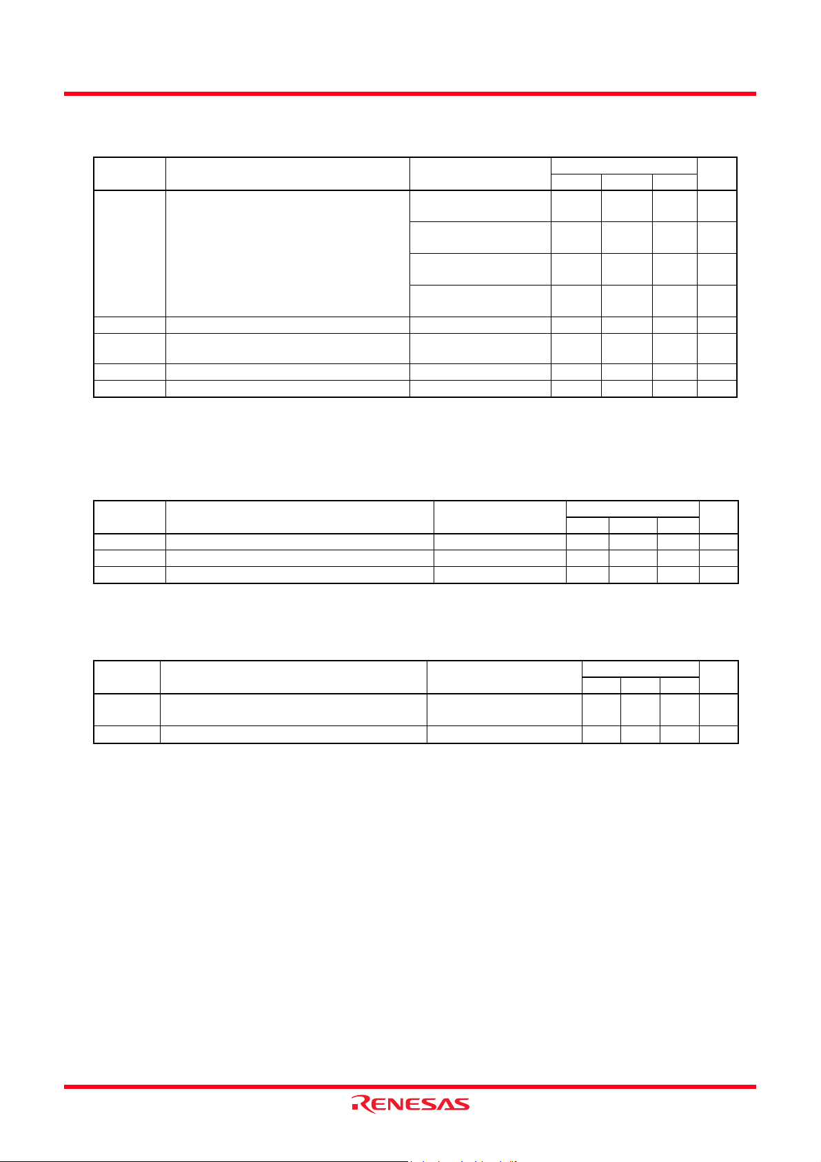
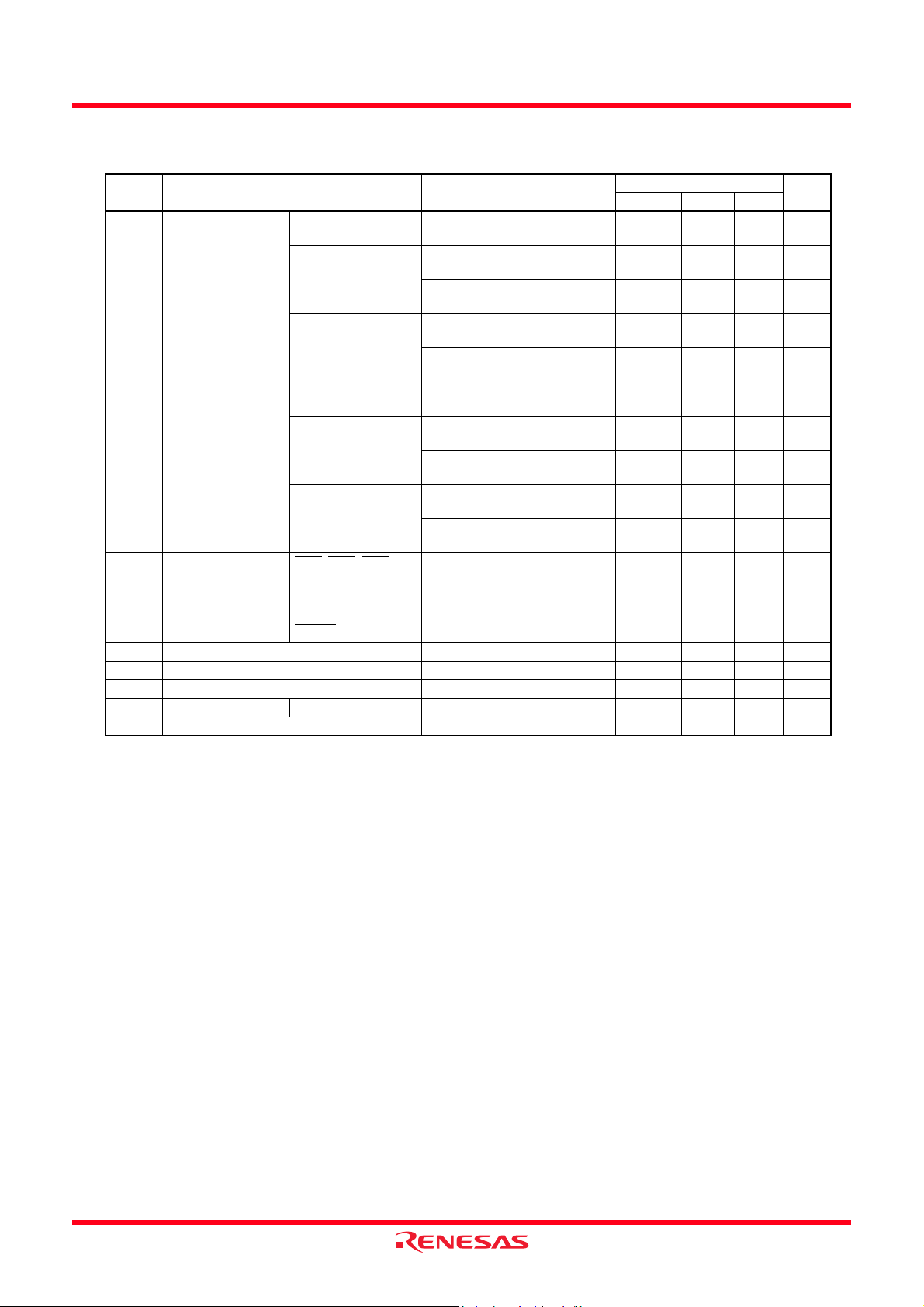
1.2 Product List
Table 1.5 lists Product List for R8C/2K Group, Figure 1.1 shows a Part Number, Memory Size, and Package of
R8C/2K Group, Table 1.6 lists Product List for R8C/2L Group, and Figure 1.2 shows a Part Number, Memory Size,
and Package of R8C/2L Group.
Table 1.5 Product List for R8C/2K Group Current of Jul. 2007
Part No. ROM Capacity RAM Capacity Package Type Remarks
R5F212K2SNFP (D) 8 Kbytes 1 Kbyte PLQP0032GB- A N versio n
R5F212K4SNFP (D) 16 Kbytes 1.5 Kbytes PLQP0032GB-A
R5F212K2SDFP (D) 8 Kbytes 1 Kbyte PLQP0032GB- A D versio n
R5F212K4SDFP (D) 16 Kbytes 1.5 Kbytes PLQP0032GB-A
(D): Under development
Part No. R 5 F 21 2K 2 S N FP
Package type:
FP: PLQP0032GB-A
Classification
N: Operating ambient temperature -20°C to 85°C
D: Operating ambient temperature -40°C to 85°C
S: Low-voltage version
ROM capacity
2: 8 KB
4: 16 KB
R8C/2K Group
R8C/Tiny Series
Memory type
F: Flash memory
Renesas MCU
Renesas semiconductor
Figure 1.1 Part Number, Memory Size, and Package of R8C/2K Group
Rev.0.10 Jul 20, 2007 Page 6 of 44
REJ03B0219-0010
Page 7
Under development
Preliminary specification
Specications in this manual are tentative and subject to change
R8C/2K Group, R8C/2L Group 1. Overview
Table 1.6 Product List for R8C/2L Group Current of Jul. 2007
Part No.
ROM Capacity
Pr o g r a m RO M Data flash
RAM
Capacity
Package Ty pe Remarks
R5F212L2SNFP (D) 8 Kbytes 1 Kbyte × 2 1 Kbyte PLQP0032GB-A N version
R5F212L4SNFP (D) 16 Kbytes 1 Kbyte × 2 1.5 Kbytes PLQP0032GB-A
R5F212L2SDFP (D) 8 Kbytes 1 Kbyte × 2 1 Kbyte PLQP0032GB-A D version
R5F212L4SDFP (D) 16 Kbytes 1 Kbyte × 2 1.5 Kbytes PLQP0032GB-A
(D): Under development
Part No. R 5 F 21 2L 2 S N FP
Package type:
FP: PLQP0032GB-A
Classification
N: Operating ambient temperature -20°C to 85°C
D: Operating ambient temperature -40°C to 85°C
S: Low-voltage version
ROM capacity
2: 8 KB
4: 16 KB
R8C/2L Group
R8C/Tiny Series
Memory type
F: Flash memory
Renesas MCU
Renesas semiconductor
Figure 1.2 Part Number, Memory Size, and Package of R8C/2L Group
Rev.0.10 Jul 20, 2007 Page 7 of 44
REJ03B0219-0010
Page 8
Under development
Preliminary specification
Specications in this manual are tentative and subject to change
R8C/2K Group, R8C/2L Group 1. Overview
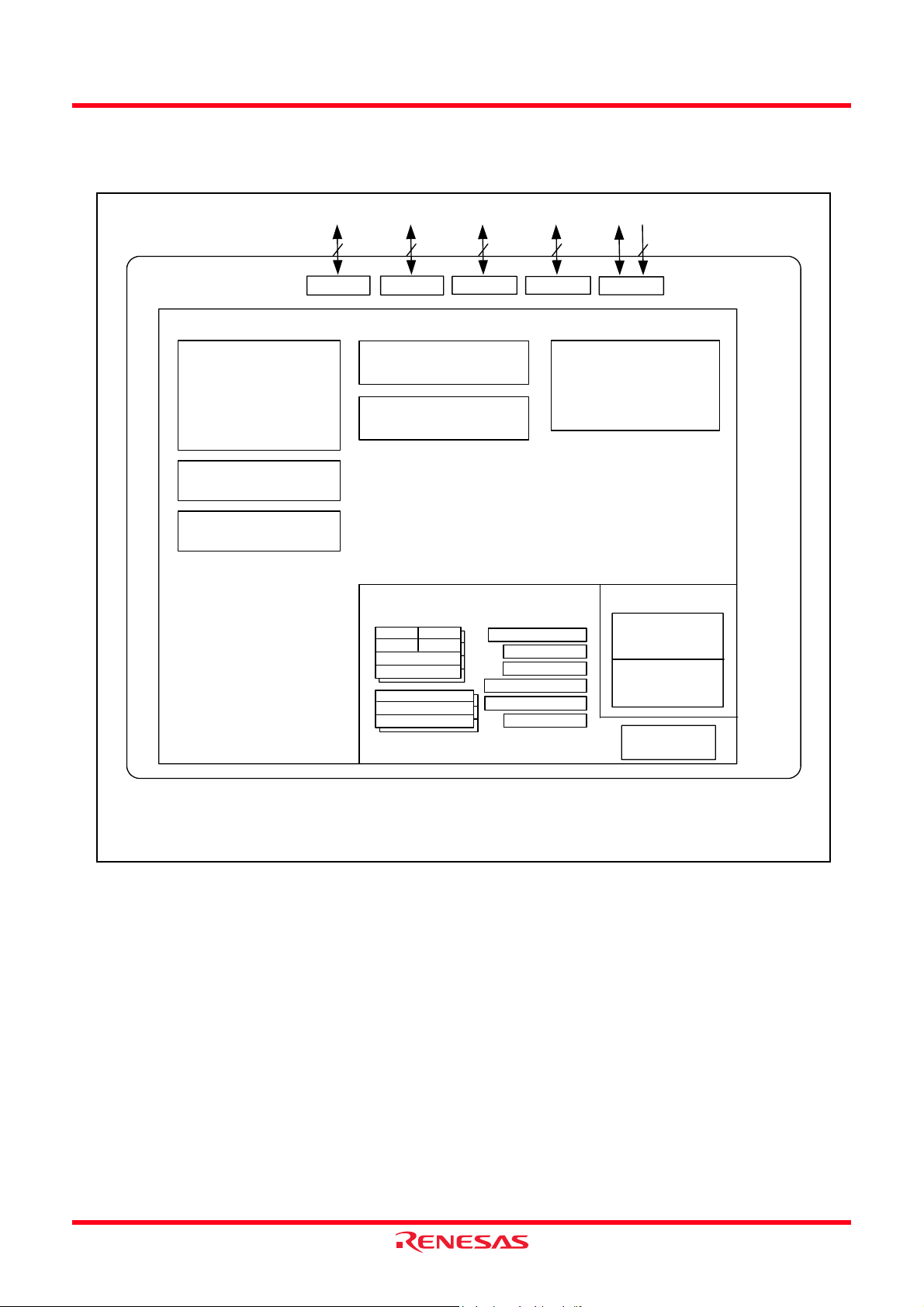
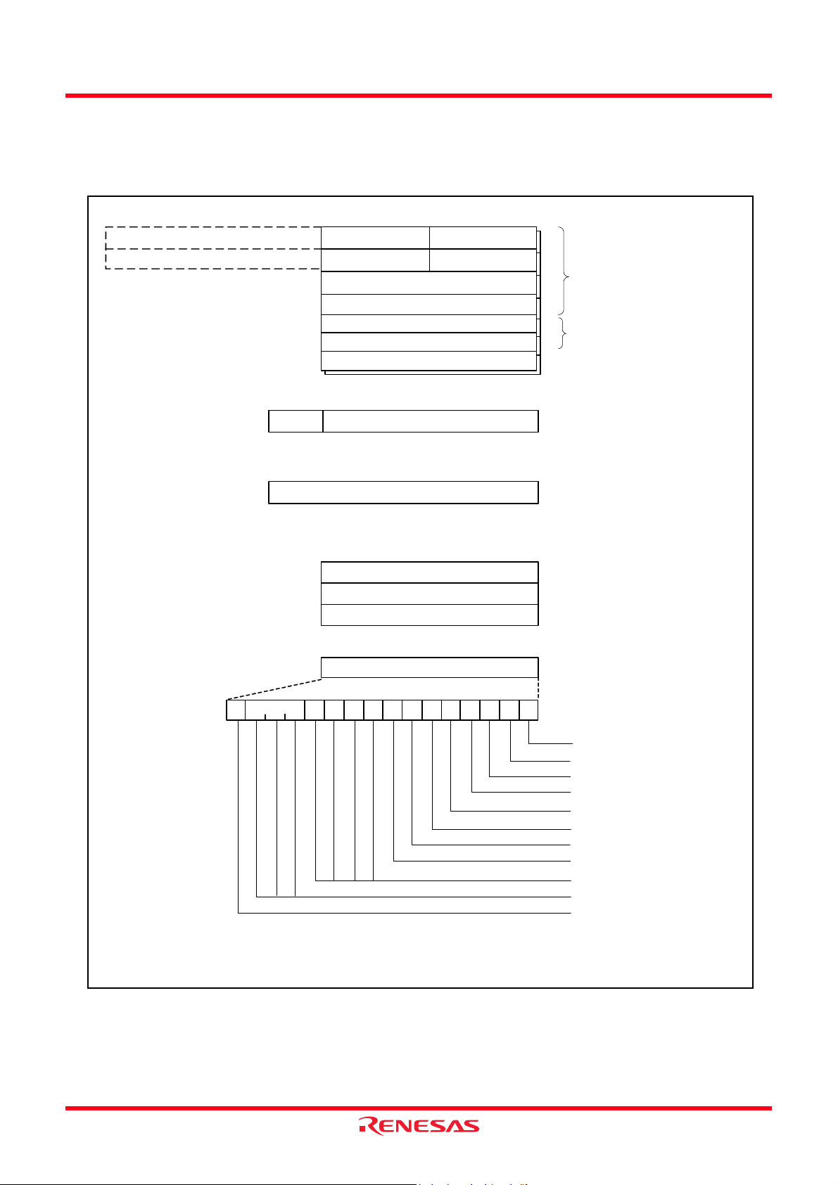
1.3 Block Diagram
Figure 1.3 shows a Block Diagram.
I/O ports
Peripheral functions
Timers
Timer RA (8 bits × 1)
Timer RB (8 bits × 1)
Timer RC (16 bits × 1)
Timer RD (16 bits × 2)
Watchdog timer
(15 bits)
A/D converter
× 9 channels)
(10 bits
Port P0
5
8
Port P1
clock synchronous serial I/O
(8 bits × 2)
LIN module
Port P2
UART or
R8C/Tiny Series CPU core
R0H R0L
R1L
R1H
R2
R3
A0
A1
FB
8
3
Port P3
High-speed on-chip oscillator
Low-speed on-chip oscillator
1 3
Port P4
System clock
generation circuit
XIN-XOUT
Memory
SB
USP
ISP
INTB
PC
FLG
(1)
ROM
(2)
RAM
Multiplier
Figure 1.3 Block Diagram
Rev.0.10 Jul 20, 2007 Page 8 of 44
REJ03B0219-0010
NOTES:
1. ROM size varies with MCU type.
2. RAM size varies with MCU type.
Page 9
Under development
Preliminary specification
Specications in this manual are tentative and subject to change
R8C/2K Group, R8C/2L Group 1. Overview
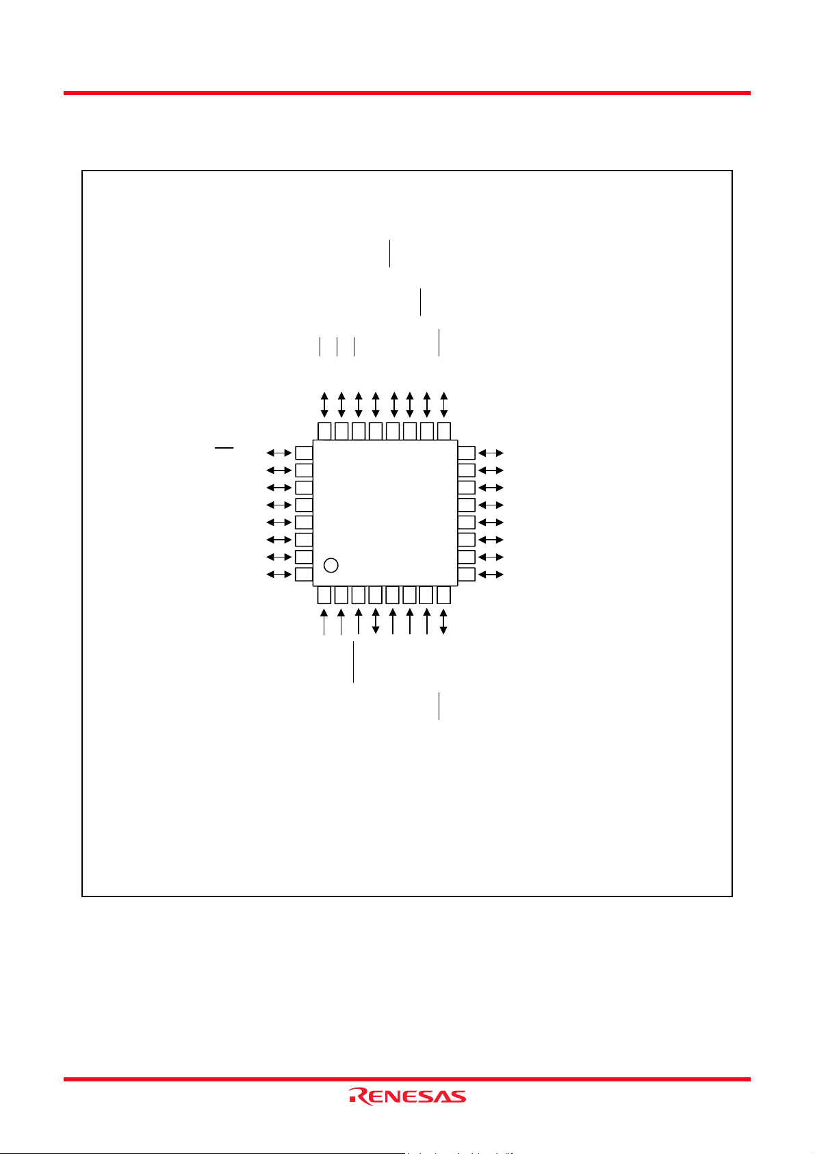
1.4 Pin Assignment
Figure 1.4 shows Pin Assignment (Top View). Table 1.7 outlines the Pin Name Information by Pin Number.
(2)
P4_5/INT0
P1_5/RXD0/(TRAIO)/(INT1)
5781234 6
P1_6/CLK0
P1_7/TRAIO/INT1
16
15
14
13
12
11
10
9
P2_0/TRDIOA0/TRDCLK
P2_2/TRDIOC0
P2_1/TRDIOB0
P2_3/TRDIOD0
P2_4/TRDIOA1
P2_5/TRDIOB1
P2_6/TRDIOC1
P2_7/TRDIOD1
P1_0/KI0/AN8
P3_4/TRCIOC
P3_5/TRCIOD
P0_5/AN2
P0_3/AN4/CLK2
P0_2/AN5/RXD2
P0_1/AN6/TXD2
P0_0/AN7
P1_4/TXD0
P1_3/KI3/AN11/TRBO
P1_1/KI1/AN9/TRCIOA/TRCTRG
P1_2/KI2/AN10/TRCIOB
24 23 22 21 20 19 18 17
25
26
27
R8C/2K Group
28
R8C/2L Group
29
30
PLQP0032GB-A
31
32
(32P6U-A)
(top view)
MODE
VREF/P4_2
NOTES:
1. P4_7 are an input-only port.
2. Can be assigned to the pin in parentheses by a program.
3. Confirm the pin 1 position on the package by referring to the package dimensions.
Figure 1.4 Pin Assignment (Top View)
(1)
RESET
XOUT/P4_7
VSS/AVSS
XIN/P4_6
VCC/AVCC
P3_3/INT3/TRCCLK
Rev.0.10 Jul 20, 2007 Page 9 of 44
REJ03B0219-0010
Page 10
Under development
Preliminary specification
Specications in this manual are tentative and subject to change
R8C/2K Group, R8C/2L Group 1. Overview
Table 1.7 Pin Name Information by Pin Number
Pin
Number
Control Pin Port
Interrupt Timer Serial Interface
1VREFP4_2
2MODE
3
RESET
4XOUTP4_7
5 VSS/AVSS
6XINP4_6
7 VCC/AVCC
8P3_3
INT3
9 P2_7 TRDIOD1
10 P2_6 TRDIOC1
11 P2_5 TRDIOB1
12 P2_4 TRDIOA1
13 P2_3 TRDIOD0
14 P2_1 TRDIOB0
15 P2_2 TRDIOC0
16 P2_0 TRDIOA0/TRDCLK
17 P4_5
18 P1_7
INT0
INT1
19 P1_6 CLK0
20 P1_5
(INT1
(1)
)
21 P1_4 TXD0
22 P1_3
23 P1_2
24 P1_1
25 P1_0
KI3
KI2
KI1
KI0
26 P3_4 TRCIOC
27 P3_5 TRCIOD
28 P0_5 AN2
29 P0_3 CLK2 AN4
30 P0_2 RXD2 AN5
31 P0_1 TXD2 AN6
32 P0_0 AN7
NOTE:
1. Can be assigned to the pin in parentheses by a program.
I/O Pin Functions for of Peripheral Modules
A/D Converter
TRCCLK
TRAIO
(TRAIO)
(1)
RXD0
TRBO AN11
TRCIOB AN10
TRCIOA/TRCTRG AN9
AN8
Rev.0.10 Jul 20, 2007 Page 10 of 44
REJ03B0219-0010
Page 11
Under development
Preliminary specification
Specications in this manual are tentative and subject to change
R8C/2K Group, R8C/2L Group 1. Overview
1.5 Pin Functions
Table 1.8 lists Pin Functions.
Table 1.8 Pin Functions
Item Pin Name
Power supply input VCC, VSS − Apply 2.2 V to 5.5 V to the VCC pin. Apply 0 V to the VSS pin.
Analog power
supply input
Reset input
MODE MODE I Connect this pin to VCC via a resistor.
XIN clock input XIN I These pins are provided for XIN clock ge neration circuit I/O.
XIN clock output XOUT O
interrupt input INT0, INT1, INT3 IINT interrupt input pins.
INT
Key input interrupt
Timer RA TRAIO I/O Timer RA I/O pin
Timer RB TRBO O Timer RB output pin
Timer RC TRCCLK I External clock input pin
Timer RD TRDIOA0, TRDIOA1,
Serial interface CLK0, CLK2 I/O Transfer clock I/O pins
Reference voltage
input
A/D converter AN2, AN4 to AN11 I Analog input pins to A/D converter
I/O port P0_0 to P0_3, P0_5,
Input port P4_2, P4_6, P4_7 I Input-only ports
I: Input O: Output I/O: Input and output
NOTE:
1. Refer to the oscillator manufacturer for oscillation characteristics.
AVCC, AVSS − Power supply for the A/D converter.
RESET
KI0 to KI3
TRCTRG I External trigger input pin
TRCIOA, TRCIOB,
TRCIOC, TRCIOD
TRDIOB0, TRDIOB1,
TRDIOC0, TRDIOC1,
TRDIOD0, TRDIOD1
TRDCLK I External clock input pin
RXD0, RXD2 I Serial data input pins
TXD0, TXD2 O Serial data output pins
VREF I Reference voltage input pin to A/D converter
P1_0 to P1_7,
P2_0 to P2_7,
P3_3 to P3_5,
P4_5,
I/O Type
Connect a capacitor between AVCC and AVSS.
I Input “L” on this pin resets the MCU.
Connect a ceramic resonator or a crystal oscillator between
the XIN and XOUT pins
the XIN pin and leave the XOUT pin open.
INT0 is timer RB, timer RC and timer RD input pins.
I Key input interrupt input pins
I/O Timer RC I/O pins
I/O Timer RD I/O pins
I/O CMOS I/O ports. Each port has an I/ O select direction
register, allowing each pin in the port to be directed for input
or output individually.
Any port set to input can be set to use a pull-up resistor or not
by a program.
P2_0 to P2_7 also function as LED drive ports.
Description
(1)
. To use an external clock, input it to
Rev.0.10 Jul 20, 2007 Page 11 of 44
REJ03B0219-0010
Page 12
Under development
Preliminary specification
Specications in this manual are tentative and subject to change
R8C/2K Group, R8C/2L Group 2. Central Processing Unit (CPU)
2. Central Processing Unit (CPU)
Figure 2.1 shows the CPU Registers. The CPU contains 13 registers. R0, R1, R2, R3, A0, A1, and FB configure a
register bank. There are two sets of register bank.
b31
R2
R3
b15 b8b7
R0H (high-order of R0)
R1H (high-order of R1)
R0L (low-order of R0)
R1L (low-order of R1)
R2
R3
A0
A1
FB
b15b19
INTBH
The 4 high order bits of INTB are INTBH and
the 16 low order bits of INTB are INTBL.
b19
INTBL
PC
b15
USP
ISP
SB
b0
Data registers
Address registers
Frame base register
b0
Interrupt table register
b0
Program counter
b0
User stack pointer
Interrupt stack pointer
Static base register
(1)
(1)
(1)
b15
IPL
NOTE:
1. These registers comprise a register bank. There are two register banks.
Figure 2.1 CPU Registers
b15
b0
FLG
b8
b7
b0
C
DZSBOIU
Flag register
Carry flag
Debug flag
Zero flag
Sign flag
Register bank select flag
Overflow flag
Interrupt enable flag
Stack pointer select flag
Reserved bit
Processor interrupt priority level
Reserved bit
Rev.0.10 Jul 20, 2007 Page 12 of 44
REJ03B0219-0010
Page 13

Under development
R8C/2K Group, R8C/2L Group 2. Central Processing Unit (CPU)
Preliminary specification
Specications in this manual are tentative and subject to change
2.1 Data Registers (R0, R1, R2, and R3)
R0 is a 16-bit register for transfer, arithmetic, and logic operations. The same applies to R1 to R3. R0 can be split
into high-order bits (R0H) and low-order bits (R0L) to be used separatel y as 8-bit data regi sters. R1H and R 1L are
analogous to R0H and R0L. R2 can be combined with R0 and used as a 32-bit data regi ster (R2R0). R3R1 is
analogous to R2R0.
2.2 Address Registers (A0 and A1)
A0 is a 16-bit register for address register indirect addressing and address register relative addressing. It is also
used for transfer, arithmetic, and logic operations. A1 is analogous to A0. A1 can be combined with A0 and as a 32bit address register (A1A0).
2.3 Frame Base Register (FB)
FB is a 16-bit register for FB relative addressing.
2.4 Interrupt Table Register (INTB)
INTB is a 20-bit register that indicates the start address of an interrupt vector table.
2.5 Program Counter (PC)
PC is 20 bits wide and indicates the address of the next instruction to be executed.
2.6 User Stack Pointer (USP) and Interrupt Stack Pointer (ISP)
The stack pointers (SP), USP, and ISP, are each 16 bits wide. The U flag of FLG is used to switch between
USP and ISP.
2.7 Static Base Register (SB)
SB is a 16-bit register for SB relative addressing.
2.8 Flag Register (FLG)
FLG is an 11-bit register indicating the CPU state.
2.8.1 Carry Flag (C)
The C flag retains carry, borrow, or shift-out bits that have been generated by the arithmetic and logic unit.
2.8.2 Debug Flag (D)
The D flag is for debugging only. Set it to 0.
2.8.3 Zero Flag (Z)
The Z flag is set to 1 when an arithmetic operation results in 0; otherwise to 0.
2.8.4 Sign Flag (S)
The S flag is set to 1 when an arithmetic operation results in a negative value; otherwise to 0.
2.8.5 Register Bank Select Flag (B)
Register bank 0 is selected when the B flag is 0. Register bank 1 is selected when this flag is set to 1.
2.8.6 Overflow Flag (O)
The O flag is set to 1 when an operation results in an overflow; otherwise to 0.
Rev.0.10 Jul 20, 2007 Page 13 of 44
REJ03B0219-0010
Page 14

Under development
R8C/2K Group, R8C/2L Group 2. Central Processing Unit (CPU)
Preliminary specification
Specications in this manual are tentative and subject to change
2.8.7 Interrupt Enable Flag (I)
The I flag enables maskable interrupts.
Interrupt are disabled when the I flag is set to 0, and are enabled when the I flag is set to 1. The I flag is set to 0
when an interrupt request is acknowledged.
2.8.8 Stack Pointer Select Flag (U)
ISP is selected when the U flag is set to 0; USP is selected when the U flag is set to 1.
The U flag is set to 0 when a hardware interrupt request is acknowledged or the INT instruction of software
interrupt numbers 0 to 31 is executed.
2.8.9 Processor Interrupt Priority Level (IPL)
IPL is 3 bits wide and assigns processor interrupt priority levels from level 0 to level 7.
If a requested interrupt has higher priority than IPL, the interrupt is enabled.
2.8.10 Reserved Bit
If necessary, set to 0. When read, the content is undefined.
Rev.0.10 Jul 20, 2007 Page 14 of 44
REJ03B0219-0010
Page 15

Under development
Preliminary specification
Specications in this manual are tentative and subject to change
R8C/2K Group, R8C/2L Group 3. Memory
3. Memory
3.1 R8C/2K Group
Figure 3.1 is a Memory Map of R8C/2K Group. The R8C/2K Group has 1 Mbyte of address space from addresses
00000h to FFFFFh.
The internal ROM is allocated lower addresses, beginning with address 0FFFFh. For example, a 16-Kbyte internal
ROM area is allocated addresses 0C000h to 0FFFFh.
The fixed interrupt vector table is allocated addresses 0FFDCh to 0FFFFh. They store the starting address of each
interrupt routine.
The internal RAM is allocated higher addresses beginning with address 00400h. For example, a 1.5-Kbyte internal
RAM area is allocated addresses 00400h to 009FFh. The internal RAM is used not only for storing data but also for
calling subroutines and as stacks when interrupt requests are acknowledged.
Special function registers (SFRs) are allocated addresses 00000h to 002FFh. The peripheral function control
registers are allocated here. All addresses within the SFR, which have nothing allocated are reserved for future use
and cannot be accessed by users.
00000h
002FFh
00400h
0XXXh
0YYYYh
0FFFFh
FFFFFh
NOTE:
1. The blank regions are reserved. Do not access locations in these regions.
R5F212K2SNFP, R5F212K2SDFP
R5F212K4SNFP, R5F212K4SDFP
SFR
(Refer to 4. Special
Function Registers
(SFRs))
Internal RAM
Internal ROM
(program ROM)
Expanded area
Part Number
0FFDCh
Watchdog timer/oscillation stop detection/voltage monitor
0FFFFh
Internal ROM Internal RAM
Size Size
8 Kbytes
16 Kbytes
Address 0YYYYh Address 0XXXXh
0E000h
0C000h
Undefined instruction
Overflow
BRK instruction
Address match
Single step
(Reserved)
(Reserved)
Reset
1 Kbyte
1.5 Kbytes
007FFh
009FFh
Figure 3.1 Memory Map of R8C/2K Group
Rev.0.10 Jul 20, 2007 Page 15 of 44
REJ03B0219-0010
Page 16

Under development
Preliminary specification
Specications in this manual are tentative and subject to change
R8C/2K Group, R8C/2L Group 3. Memory
3.2 R8C/2L Group
Figure 3.2 is a Memory Map of R8C/2L Group. The R8C/2L Group has 1 Mbyte of address space from addresses
00000h to FFFFFh.
The internal ROM (program ROM) is allocated lower addresses, beginning with address 0FFFFh. For example, a
16-Kbyte internal ROM area is allocated addresses 0C000h to 0FFFFh.
The fixed interrupt vector table is allocated addresses 0FFDCh to 0FFFFh. They store the starting address of each
interrupt routine.
The internal ROM (data flash) is allocated addresses 02400h to 02BFFh.
The internal RAM area is allocated higher addresses, beginning with address 00400h. For example, a 1.5-Kbyte
internal RAM is allocated addresses 00400h to 009FFh. The internal RAM is used not only for storing data but also
for calling subroutines and as stacks when interrupt requests are acknowledged.
Special function registers (SFRs) are allocated addresses 00000h to 002FFh. The peripheral function control
registers are allocated here. All addresses within the SFR, which have nothing allocated are reserved for future use
and cannot be accessed by users.
00000h
002FFh
00400h
0XXXXh
02400h
02BFFh
0YYYYh
0FFFFh
FFFFFh
NOTES:
1. Data flash block A (1 Kbyte) and B (1 Kbyte) are shown.
2. The blank regions are reserved. Do not access locations in these regions.
R5F212L2SNFP, R5F212L2SDFP
R5F212L4SNFP, R5F212L4SDFP
SFR
(Refer to 4. Special
Function Registers
(SFRs))
Internal RAM
Internal ROM
(data flash)
Internal ROM
(program ROM)
Expanded area
Part Number
(1)
0FFDCh
Watchdog timer/oscillation stop detection/voltage monitor
0FFFFh
Internal ROM
Size Size
8 Kbytes
16 Kbytes
Address 0YYYYh Address 0XXXXh
0E000h
0C000h
Undefined instruction
Overflow
BRK instruction
Address match
Single step
(Reserved)
(Reserved)
Reset
1 Kbyte
1.5 Kbytes
007FFh
009FFh
Figure 3.2 Memory Map of R8C/2L Group
Rev.0.10 Jul 20, 2007 Page 16 of 44
REJ03B0219-0010
Page 17

Under development
Preliminary specification
Specications in this manual are tentat ive and subject to change
R8C/2K Group, R8C/2L Group 4. Special Function Register s (SFRs)
4. Special Function Registers (SFRs)
An SFR (special function register) is a control register for a peripheral function. Tables 4.1 to 4.7 list the special
function registers.
Table 4.1 SFR Information (1)
Address Register Symbol After reset
0000h
0001h
0002h
0003h
0004h Processor Mode Register 0 PM0 00h
0005h Processor Mode Register 1 PM1 00h
0006h System Clock Control Register 0 CM0 01101000b
0007h System Clock Control Register 1 CM1 00100000b
0008h
0009h
000Ah Protect Register PRCR 00h
000Bh
000Ch Oscillation Stop Detection Register OCD 00000100b
000Dh Watchdog Timer Reset Register WDTR XXh
000Eh Watchdog Timer Start Register WDTS XXh
000Fh Watchdog Timer Control Register WDC 00X11111b
0010h Address Match Interrupt Register 0 RMAD0 00h
0011h 00h
0012h 00h
0013h Address Match Interrupt Enable Register AIER 00h
0014h Address Match Interrupt Register 1 RMAD1 00h
0015h 00h
0016h 00h
0017h
0018h
0019h
001Ah
001Bh
001Ch Count Source Protection Mode Register CSPR 00h
001Dh
001Eh
001Fh
0020h
0021h
0022h
0023h High-Speed On-Chip Oscillator Control Register 0 FRA0 00h
0024h High-Speed On-Chip Oscillator Control Register 1 FRA1 When shipping
0025h High-Speed On-Chip Oscillator Control Register 2 FRA2 00h
0026h
0027h
0028h
0029h
002Ah
002Bh High-Speed On-Chip Oscillator Control Register 6 FRA6 When Shipping
0030h
0031h
0032h
0033h
0034h
0035h
0036h
0037h
0038h
0039h
003Ah
003Bh
003Ch
003Dh
003Eh
003Fh
X: Undefined
NOTES:
1. The blank regions are reserved. Do not access locations in these regions.
2. Software reset, watchdog timer reset, voltage monitor 1 reset, or voltage monitor 2 reset do not affect this register.
3. The LVD0ON bit in the OFS regist er is set to 1 and hardware reset.
4. Power-on reset, voltage monitor 0 reset, or the LVD0ON bit in the OFS register is set to 0 and hardware reset.
5. Software reset, watchdog timer reset, voltage monitor 1 reset, or voltage monitor 2 reset do not affect b2 and b3.
6. The CSPROINI bit in the OFS register is set to 0.
Voltage Detection Register 1
Voltage Detection Register 2
Voltage Monitor 1 Circuit Control Regist er
Voltage Monitor 2 Circuit Control Regist er
Voltage Monitor 0 Circuit Control Regist er
(1)
10000000b
(2)
(2)
(5)
(5)
(2)
VCA1 00001000b
VCA2
VW1C 00001000b
VW2C 00h
VW0C
(3)
00h
00100000b
0000X000b
0100X001b
(6)
(4)
(3)
(4)
Rev.0.10 Jul 20, 2007 Page 17 of 44
REJ03B0219-0010
Page 18

Under development
Preliminary specification
Specications in this manual are tentat ive and subject to change
R8C/2K Group, R8C/2L Group 4. Special Function Register s (SFRs)
Table 4.2 SFR Information (2)
Address Register Symbol After reset
0040h
0041h
0042h
0043h
0044h
0045h
0046h
0047h Timer RC Interrupt Control Register TRCIC XXXXX000b
0048h Timer RD0 Interrupt Control Register TRD0IC XXXXX000b
0049h Timer RD1 Interrupt Control Register TRD1IC XXXXX000b
004Ah
004Bh UART2 Transmit Interrupt Control Register S2TIC XXXXX000b
004Ch UART2 Receive Interrupt Control Register S2RIC XXXXX000b
004Dh Key Input Interrupt Control Register KUPIC XXXXX000b
004Eh A/D Conversion Interrupt Control Register ADIC XXXXX000b
004Fh
0050h
0051h UART0 Transmit Interrupt Control Register S0TIC XXXXX000b
0052h UART0 Receive Interrupt Control Register S0RIC XXXXX000b
0053h
0054h
0055h
0056h Timer RA Interrupt Control Register TRAIC XXXXX000b
0057h
0058h Timer RB Interrupt Control Register TRBIC XXXXX000b
0059h INT1 Interrupt Control Register INT1IC XX00X000b
005Ah INT3 Interrupt Control Register INT3IC XX00X000b
005Bh
005Ch
005Dh INT0 Interrupt Control Register INT0IC XX00X000b
005Eh
005Fh
0060h
0061h
0062h
0063h
0064h
0065h
0066h
0067h
0068h
0069h
006Ah
006Bh
006Ch
006Dh
006Eh
006Fh
0070h
0071h
0072h
0073h
0074h
0075h
0076h
0077h
0078h
0079h
007Ah
007Bh
007Ch
007Dh
007Eh
007Fh
X: Undefined
NOTE:
1. The blank regions are reserved. Do not access locations in these regions.
(1)
Rev.0.10 Jul 20, 2007 Page 18 of 44
REJ03B0219-0010
Page 19

Under development
Preliminary specification
Specications in this manual are tentat ive and subject to change
R8C/2K Group, R8C/2L Group 4. Special Function Register s (SFRs)
Table 4.3 SFR Information (3)
Address Register Symbol After reset
0080h
0081h
0082h
0083h
0084h
0085h
0086h
0087h
0088h
0089h
008Ah
008Bh
008Ch
008Dh
008Eh
008Fh
0090h
0091h
0092h
0093h
0094h
0095h
0096h
0097h
0098h
0099h
009Ah
009Bh
009Ch
009Dh
009Eh
009Fh
00A0h UART0 Transmit/Receive Mode Register U0MR 00h
00A1h UART0 Bit Rate Register U0BRG XXh
00A2h UART0 Transmit Buffer Register U0TB XXh
00A3h XXh
00A4h UART0 Transmit/Receive Control Register 0 U0C0 00001000b
00A5h UART0 Transmit/Receive Control Register 1 U0C1 00000010b
00A6h UART0 Receive Buffer Register U0RB XXh
00A7h XXh
00A8h
00A9h
00AAh
00ABh
00ACh
00ADh
00AEh
00AFh
00B0h
00B1h
00B2h
00B3h
00B4h
00B5h
00B6h
00B7h
00B8h
00B9h
00BAh
00BBh
00BCh
00BDh
00BEh
00BFh
X: Undefined
NOTE:
1. The blank regions are reserved. Do not access locations in these regions.
(1)
Rev.0.10 Jul 20, 2007 Page 19 of 44
REJ03B0219-0010
Page 20

Under development
Preliminary specification
Specications in this manual are tentat ive and subject to change
R8C/2K Group, R8C/2L Group 4. Special Function Register s (SFRs)
Table 4.4 SFR Information (4)
Address Register Symbol After reset
00C0h A/D Register AD XXh
00C1h XXh
00C2h
00C3h
00C4h
00C5h
00C6h
00C7h
00C8h
00C9h
00CAh
00CBh
00CCh
00CDh
00CEh
00CFh
00D0h
00D1h
00D2h
00D3h
00D4h A/D Control Register 2 ADCON2 00001000b
00D5h
00D6h A/D Control Register 0 ADCON0 00000011b
00D7h A/D Control Register 1 ADCON1 00h
00D8h
00D9h
00DAh
00DBh
00DCh
00DDh
00DEh
00DFh
00E0h Port P0 Register P0 XXh
00E1h Port P1 Register P1 XXh
00E2h Port P0 Direction Registe r PD0 00h
00E3h Port P1 Direction Registe r PD1 00h
00E4h Port P2 Register P2 XXh
00E5h Port P3 Register P3 XXh
00E6h Port P2 Direction Registe r PD2 00h
00E7h Port P3 Direction Registe r PD3 00h
00E8h Port P4 Register P4 XXh
00E9h
00EAh Port P4 Direction Register PD4 00h
00EBh
00ECh
00EDh
00EEh
00EFh
00F0h
00F1h
00F2h
00F3h
00F4h Port P2 Drive Capacity Control Register P2DRR 00h
00F5h
00F6h
00F7h
00F8h
00F9h External Input Enable Register INTEN 00h
00FAh INT Input Filter Select Register INTF 00h
00FBh Key Input Enable Register KIEN 00h
00FCh Pull-Up Control Register 0 PUR0 00h
00FDh Pull-Up Control Register 1 PUR1 XX000000b
00FEh
00FFh
X: Undefined
NOTE:
1. The blank regions are reserved. Do not access locations in these regions.
(1)
Rev.0.10 Jul 20, 2007 Page 20 of 44
REJ03B0219-0010
Page 21

Under development
Preliminary specification
Specications in this manual are tentat ive and subject to change
R8C/2K Group, R8C/2L Group 4. Special Function Register s (SFRs)
Table 4.5 SFR Information (5)
Address Register Symbol After reset
0100h Timer RA Control Register TRACR 00h
0101h Timer RA I/O Control Register TRAIOC 00h
0102h Timer RA Mode Register TRAMR 00h
0103h Timer RA Prescaler Register TRAPRE FFh
0104h Timer RA Register TRA FFh
0105h LIN Control Register 2 LINCR2 00h
0106h LIN Control Register LINCR 00h
0107h LIN Status Register LINST 00h
0108h Timer RB Control Register TRBCR 00h
0109h Timer RB One-Shot Control Register TRBOCR 00h
010Ah Timer RB I/O Control Register TRBIOC 00h
010Bh Timer RB Mode Register TRBMR 00h
010Ch Timer RB Prescaler Register TRBPRE FFh
010Dh Timer RB Secondary Register TRBSC FFh
010Eh Timer RB Primary Register TRBPR FFh
010Fh
0110h
0111h
0112h
0113h
0114h
0115h
0116h
0117h
0118h
0119h
011Ah
011Bh
011Ch
011Dh
011Eh
011Fh
0120h Timer RC Mode Register TRCMR 01001000b
0121h Timer RC Control Register 1 TRCCR1 00h
0122h Timer RC Interrupt Enable Register TRCIER 011 10000b
0123h Timer RC Status Register TRCSR 01110000b
0124h Timer RC I/O Control Register 0 TRCIOR0 10001000b
0125h Timer RC I/O Control Register 1 TRCIOR1 10001000b
0126h Timer RC Counter TRC 00h
0127h 00h
0128h Timer RC General Register A TRCGRA FFh
0129h FFh
012Ah Timer RC General Register B TRCGRB FFh
012Bh FFh
012Ch Timer RC General Register C TRCGRC FFh
012Dh FFh
012Eh Timer RC General Register D TRCGRD FFh
012Fh FFh
0130h Timer RC Control Register 2 TRCCR2 00011111b
0131h Timer RC Digital Filter Function Select Register TRCDF 00h
0132h Timer RC Output Master Enable Register TRCOER 01111111b
0133h
0134h
0135h
0136h
0137h Timer RD Start Register TRDSTR 11111100b
0138h Timer RD Mode Register TRDMR 00001110b
0139h Timer RD PWM Mode Register TRDPMR 10001000b
013Ah Timer RD Function Control Register TRDFCR 10000000b
013Bh Timer RD Output Master Enable Register 1 TRDOER1 FFh
013Ch Timer RD Output Master Enable Register 2 TRDOER2 01111111b
013Dh Timer RD Output Control Register TRDOCR 00h
013Eh Timer RD Digital Filter Function Select Register 0 TRDDF0 00h
013Fh Timer RD Digital Filter Function Select Register 1 TRDDF1 00h
NOTE:
1. The blank regions are reserved. Do not access locations in these regions
(1)
Rev.0.10 Jul 20, 2007 Page 21 of 44
REJ03B0219-0010
Page 22

Under development
Preliminary specification
Specications in this manual are tentat ive and subject to change
R8C/2K Group, R8C/2L Group 4. Special Function Register s (SFRs)
Table 4.6 SFR Information (6)
Address Register Symbol After reset
0140h Timer RD Control Register 0 TRDCR0 00h
0141h Timer RD I/O Control Register A0 TRDIORA0 10001000b
0142h Timer RD I/O Control Register C0 TRDIORC0 10001000b
0143h Timer RD Status Register 0 TRDSR0 11000000b
0144h Timer RD Interrupt Enable Register 0 TRDIER0 11100000b
0145h Timer RD PWM Mode Output Level Control Register 0 TRDPOCR0 11111000b
0146h Timer RD Counter 0 TRD0 00h
0147h 00h
0148h Timer RD General Register A0 TRDGRA0 FFh
0149h FFh
014Ah Timer RD General Register B0 TRDGRB0 FFh
014Bh FFh
014Ch Timer RD General Register C0 TRDGRC0 FFh
014Dh FFh
014Eh Timer RD General Register D0 TRDGRD0 FFh
014Fh FFh
0150h Timer RD Control Register 1 TRDCR1 00h
0151h Timer RD I/O Control Register A1 TRDIORA1 10001000b
0152h Timer RD I/O Control Register C1 TRDIORC1 10001000b
0153h Timer RD Status Register 1 TRDSR1 11000000b
0154h Timer RD Interrupt Enable Register 1 TRDIER1 11100000b
0155h Timer RD PWM Mode Output Level Control Register 1 TRDPOCR1 11111000b
0156h Timer RD Counter 1 TRD1 00h
0157h 00h
0158h Timer RD General Register A1 TRDGRA1 FFh
0159h FFh
015Ah Timer RD General Register B1 TRDGRB1 FFh
015Bh FFh
015Ch Timer RD General Register C1 TRDGRC1 FFh
015Dh FFh
015Eh Timer RD General Register D1 TRDGRD1 FFh
015Fh FFh
0160h UART2 Transmit/Receive Mode Register U2MR 00h
0161h UART2 Bit Rate Register U2BRG XXh
0162h UART2 Transmit Buff er Regist er U2TB XXh
0163h XXh
0164h UART2 Transmit/Receive Control Register 0 U2C0 00001000b
0165h UART2 Transmit/Receive Control Register 1 U2C1 00000010b
0166h UART2 Receive Buffer Register U2RB XXh
0167h XXh
0168h
0169h
016Ah
016Bh
016Ch
016Dh
016Eh
016Fh
0170h
0171h
0172h
0173h
0174h
0175h
0176h
0177h
0178h
0179h
017Ah
017Bh
017Ch
017Dh
017Eh
017Fh
X: Undefined
NOTE:
1. The blank regions are reserved. Do not access locations in these regions.
(1)
Rev.0.10 Jul 20, 2007 Page 22 of 44
REJ03B0219-0010
Page 23

Under development
Preliminary specification
Specications in this manual are tentat ive and subject to change
R8C/2K Group, R8C/2L Group 4. Special Function Register s (SFRs)
Table 4.7 SFR Information (7)
Address Register Symbol After reset
0180h
0181h
0182h
0183h
0184h
0185h
0186h
0187h
0188h
0189h
018Ah
018Bh
018Ch
018Dh
018Eh
018Fh
0190h
0191h
0192h
0193h
0194h
0195h
0196h
0197h
0198h
0199h
019Ah
019Bh
019Ch
019Dh
019Eh
019Fh
01A0h
01A1h
01A2h
01A3h
01A4h
01A5h
01A6h
01A7h
01A8h
01A9h
01AAh
01ABh
01ACh
01ADh
01AEh
01AFh
01B0h
01B1h
01B2h
01B3h Flash Memory Control Register 4 FMR4 01000000b
01B4h
01B5h Flash Memory Control Register 1 FMR1 1000000Xb
01B6h
01B7h Flash Memory Control Register 0 FMR0 00000001b
01B8h
01B9h
01BAh
01BBh
01BCh
01BDh
01BEh
01BFh
FFFFh Option Function Select Register OFS (Note 2)
X: Undefined
NOTE:
1. The blank regions are reserved. Do not access locations in these regions.
2. The OFS register cannot be changed by a program. Use a flash programmer to write to it.
(1)
Rev.0.10 Jul 20, 2007 Page 23 of 44
REJ03B0219-0010
Page 24

Under development
Preliminary specification
Specications in this manual are tentat ive and subject to change
R8C/2K Group, R8C/2L Group 5. Electrical Characteristics
5. Electrical Characteristics
Table 5.1 Absolute Maximum Ratings
Symbol Parameter Condition Rated Value Unit
CC/AVCC Supply voltage −0.3 to 6.5 V
V
I Input voltage −0.3 to VCC + 0.3 V
V
O Output voltage −0.3 to VCC + 0.3 V
V
d Power dissipation Topr = 25°C500mW
P
opr Operating ambient temperature −20 to 85 (N version) /
T
−40 to 85 (D version)
stg Storage temperature −65 to 150 °C
T
Table 5.2 Recommended Operating Conditions
Symbol Parameter Conditions
CC Supply voltage 2.2 − 5.5 V
V
AV
CC Supply voltage 2.7 − 5.5
V
SS/AVSS Supply voltage − 0 − V
IH Input “H” voltage 0.8 VCC − VCC V
V
V
IL Input “L” voltage 0 − 0.2 VCC V
I
OH(sum) Peak sum output
Sum of all pins IOH(peak) −−−160 mA
Min. Typ. Max.
“H” current
OH(sum) Average sum
I
Sum of all pins IOH(avg) −−−80 mA
output “H” current
OH(peak) Peak output “H”
I
current
OH(avg) Average output
I
“H” current
OL(sum) Peak sum output
I
Except P2_0 to P2_7 −−−10 mA
P2_0 to P2_7 −−−40 mA
Except P2_0 to P2_7 −−−5mA
P2_0 to P2_7 −−−20 mA
Sum of all pins IOL(peak) −−160 mA
“L” currents
OL(sum) Average sum
I
Sum of all pins I
OL(avg) −−80 mA
output “L”
currents
IOL(peak) Peak output “L”
currents
OL(avg) Average output
I
“L” current
(XIN) XIN clock input oscillation frequency 3.0 V ≤ VCC ≤ 5.5 V 0 − 20 MHz
f
− System clock OCD2 = 0
Except P2_0 to P2_7 −−10 mA
P2_0 to P2_7 −−40 mA
Except P2_0 to P2_7 −−5mA
P2_0 to P2_7 −−20 mA
XlN clock selected
OCD2 = 1
On-chip oscillator clock
selected
2.7 V ≤ V
2.2 V ≤ V
3.0 V ≤ V
2.7 V ≤ V
2.2 V ≤ V
FRA01 = 0
Low-speed on-chip
oscillator clock selected
CC < 3.0 V 0 − 10 MHz
CC < 2.7 V 0 − 5MHz
CC ≤ 5.5 V 0 − 20 MHz
CC < 3.0 V 0 − 10 MHz
CC < 2.7 V 0 − 5MHz
FRA01 = 1
High-speed on-chip
oscillator clock selected
3.0 V ≤ V
CC ≤ 5.5 V
FRA01 = 1
High-speed on-chip
oscillator clock selected
2.7 V ≤ V
CC ≤ 5.5 V
FRA01 = 1
High-speed on-chip
oscillator clock selected
2.2 V ≤ V
CC ≤ 5.5 V
NOTES:
1. V
CC = 2.2 to 5.5 V at Topr = −20 to 85°C (N version) / −40 to 85°C (D version), unless otherwise specified.
2. The typical values when average output current is 100 ms.
Standard
− 125 − kHz
−−20 MHz
−−10 MHz
−−5MHz
°C
Unit
Rev.0.10 Jul 20, 2007 Page 24 of 44
REJ03B0219-0010
Page 25

Under development
Preliminary specification
Specications in this manual are tentat ive and subject to change
R8C/2K Group, R8C/2L Group 5. Electrical Characteristics
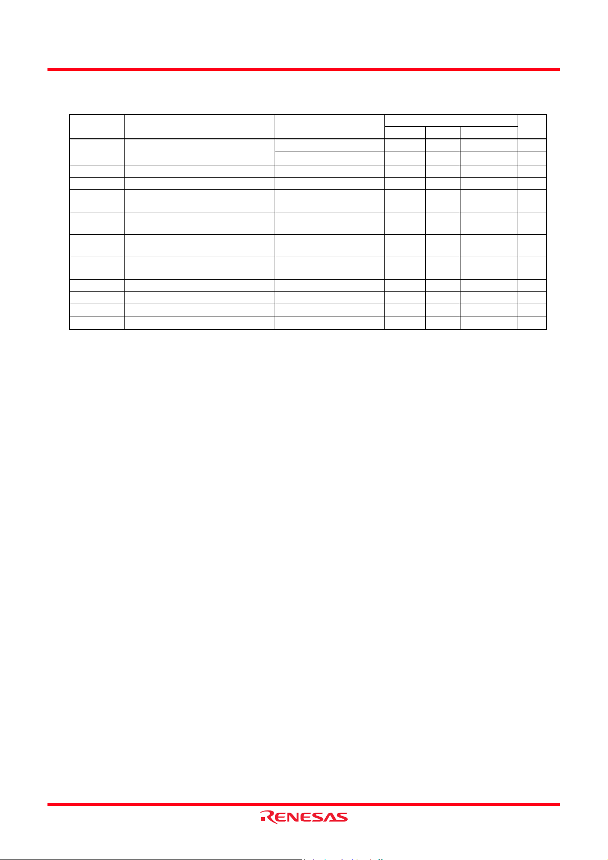
Ta ble 5.3 A /D Converter Characteristics
Symbol Parameter Conditions
− Resolution V
− Absolute
accuracy
10-bit mode φ
8-bit mode φ
10-bit mode φ
8-bit mode φ
ladder Resistor ladder Vref = AVCC 10 − 40 kΩ
R
conv Conversion time 10-bit mode φAD = 10 MHz, Vref = AVCC = 5.0 V 3.3 −−µs
t
8-bit mode φ
ref Reference voltage 2.2 − AVCC V
V
IA
V
Analog input voltage
− A/D operating
clock frequency
(2)
Without sample and hold V
With sample and hold V
ref = AVCC −−10 Bits
AD = 10 MHz, Vref = AVCC = 5.0 V −−±3 LSB
AD = 10 MHz, Vref = AVCC = 5.0 V −−±2 LSB
AD = 10 MHz, Vref = AVCC = 3.3 V −−±5 LSB
AD = 10 MHz, Vref = AVCC = 3.3 V −−±2 LSB
AD = 10 MHz, Vref = AVCC = 5.0 V 2.8 −−µs
ref = AVCC = 2.7 to 5.5 V 0.25 − 10 MHz
ref = AVCC = 2.7 to 5.5 V 1 − 10 MHz
NOTES:
1. AV
CC = 2.7 to 5.5 V at Topr = −20 to 85°C (N version) / −40 to 85°C (D version), unless otherwise specified.
2. When the analog input voltage is over the reference voltage, the A/D conversion result will be 3FFh in 10-bit mode and FFh in
8-bit mode.
Standard
Min. Typ. Max.
0 − AVCC V
Unit
P0
P1
P2
P3
P4
Figure 5.1 Ports P0 to P4 Timing Measurement Circuit
30pF
Rev.0.10 Jul 20, 2007 Page 25 of 44
REJ03B0219-0010
Page 26
Under development
Preliminary specification
Specications in this manual are tentat ive and subject to change
R8C/2K Group, R8C/2L Group 5. Electrical Characteristics
Ta ble 5.4 Flash Memory (Program ROM) Electrical Characteristics
Symbol Parameter Conditions
−
Program/erase endurance
(2)
R8C/2K Group
R8C/2L Group
Min. Typ. Max.
100
1,000
− Byte program time − 50 400 µs
− Block erase time − 0.4 9 s
d(SR-SUS) Time delay from suspend request until
t
−−97+CPU clock
suspend
− Interval from erase start/restart until
650 −−µs
following suspend request
− Interval from program start/restart until
0 −−ns
following suspend request
− Time from suspend until program/erase
−−3+CPU clock
restart
− Program, erase voltage 2.7 − 5.5 V
− Read voltage 2.2 − 5.5 V
− Program, erase temperature 0 − 60 °C
−
Data hold time
(7)
Ambient temperature = 55°C20 −−year
NOTES:
1. V
CC = 2.7 to 5.5 V at Topr = 0 to 60°C, unless otherwise specified.
2. Definition of programming/erasure endurance
The programming and erasure endurance is defined on a per-block basis.
If the programming and erasure endurance is n (n = 100 or 10,000), each block can be erased n times. For example, if 1,024
1-byte writes are performed to block A, a 1 Kbyte block, and then the block is erased, the programming/erasure endurance
still stands at one.
However, the same address must not be programmed more than once per erase operation (overwriting prohibited).
3. Endurance to guarantee all electrical characteristics after program and erase. (1 to Min. value can be guaranteed).
4. In a system that executes multiple programming operations, the actual erasure count can be reduced by writing to sequential
addresses in turn so that as much of the block as possible is used up before performing an erase operation. For example,
when programming groups of 16 bytes, the effective number of rewrites can be minimized by programming up to 128 groups
before erasing them all in one operation. It is also advisable to retain data on the erase count of each block and limit the
number of erase operations to a certain number.
5. If an error occurs during block erase, attempt to execute the clear status register command, then execute the block erase
command at least three times until the erase error does not occur.
6. Customers desiring program/erase failure rate information should contact their Renesas technical support representative.
7. The data hold time includes time that the power supply is off or the clock is not supplied.
Standard
(3)
−−times
(3)
−−times
Unit
µs
× 6 cycles
µs
× 4 cycles
Rev.0.10 Jul 20, 2007 Page 26 of 44
REJ03B0219-0010
Page 27

Under development
Preliminary specification
Specications in this manual are tentat ive and subject to change
R8C/2K Group, R8C/2L Group 5. Electrical Characteristics
Table 5.5 Flash Memory (Data flash Block A, Block B) Electrical Characteristics
Symbol Parameter Conditions
−
Program/erase endurance
(2)
− Byte program time
Min. Typ. Max.
10,000
Standard
(3)
− 50 400 µs
(4)
−−times
(program/erase endurance ≤ 1,000 times)
− Byte program time
− 65 −µs
(program/erase endurance > 1,000 times)
− Block erase time
− 0.2 9 s
(program/erase endurance ≤ 1,000 times)
− Block erase time
− 0.3 − s
(program/erase endurance > 1,000 times)
t
d(SR-SUS) Time delay from suspend request until
suspend
− Interval from erase start/restart until
−−97+CPU clock
× 6 cycles
650 −−µs
following suspend request
− Interval from program start/restart until
0 −−ns
following suspend request
− Time from suspend until program/erase
restart
−−3+CPU clock
× 4 cycles
− Program, erase voltage 2.7 − 5.5 V
− Read voltage 2.2 − 5.5 V
(8)
− Program, erase temperature
−
NOTES:
1. VCC = 2.7 to 5.5 V at Topr = −20 to 85°C (N version) / −40 to 85°C (D version), unless otherwise specified.
Data hold time
(9)
Ambient temperature = 55 °C20 −−year
−20
− 85 °C
2. Definition of programming/erasure endurance
The programming and erasure endurance is defined on a per-block basis.
If the programming and erasure endurance is n (n = 100 or 10,000), each block can be erased n times. For example, if 1,024
1-byte writes are performed to block A, a 1 Kbyte block, and then the block is erased, the programming/erasure endurance
still stands at one.
However, the same address must not be programmed more than once per erase operation (overwriting prohibited).
3. Endurance to guarantee all electrical characteristics after program and erase. (1 to Min. value can be guaranteed).
4. Standard of block A and block B when program and erase endurance exceeds 1,000 times. Byte program time to 1,000 times
is the same as that in program ROM.
5. In a system that executes multiple programming operations, the actual erasure count can be reduced by writing to sequential
addresses in turn so that as much of the block as possible is used up before performing an erase operation. For example,
when programming groups of 16 bytes, the effective number of rewrites can be minimized by programming up to 128 groups
before erasing them all in one operation. It is also advisable to retain data on the erase count of each block and limit the
number of erase operations to a certain number.
6. If an error occurs during block erase, attempt to execute the clear status register command, then execute the block erase
command at least three times until the erase error does not occur.
7. Customers desiring program/erase failure rate information should contact their Renesas technical support representative.
8. −40°C for D version.
9. The data hold time includes time that the power supply is off or the clock is not supplied.
Unit
µs
µs
Rev.0.10 Jul 20, 2007 Page 27 of 44
REJ03B0219-0010
Page 28

Under development
Preliminary specification
Specications in this manual are tentat ive and subject to change
R8C/2K Group, R8C/2L Group 5. Electrical Characteristics
Suspend request
(maskable interrupt request)
FMR46
Fixed time
Clock-dependent
time
Access restart
td(SR-SUS)
Figure 5.2 Time delay until Suspend
Table 5.6 Voltage Detection 0 Circuit Electrical Characteristics
Symbol Parameter Condition
det0 Voltage detection level 2.2 2.3 2.4 V
V
− Voltage detection circuit self power consumption VCA25 = 1, V
d(E-A) Waiting time until voltage detection circuit operation
t
starts
(2)
CC = 5.0 V − 0.9 −µA
Vccmin MCU operating voltage minimum value 2.2 −−V
NOTES:
1. The measurement condition is V
CC = 2.2 V to 5.5 V and Topr = −20 to 85°C (N version) / −40 to 85°C (D version).
2. Necessary time until the voltage detection circuit operates when setting to 1 again after setting the VCA25 bit in the VCA2
register to 0.
Standard
Min. Typ. Max.
−−300 µs
Unit
Table 5.7 Voltage Detection 1 Circuit Electrical Characteristics
Symbol Parameter Condition
det1
V
−
Voltage detection level
Voltage monitor 1 interrupt request generation time
− Voltage detection circuit self power consumption VCA26 = 1, V
d(E-A) Waiting time until voltage detection circuit operation
t
starts
(3)
(4)
(2)
CC = 5.0 V − 0.6 −µA
NOTES:
1. The measurement condition is V
2. Time until the voltage monitor 1 interrupt request is generated after the voltage passes V
CC = 2.2 V to 5.5 V and Topr = −20 to 85°C (N version) / −40 to 85°C (D version).
det1.
3. Necessary time until the voltage detection circuit operates when setting to 1 again after setting the VCA26 bit in the VCA2
register to 0.
4. This parameter shows the voltage detection level when the power supply drops.
The voltage detection level when the power supply rises is higher than the voltage detection level when the power supply
drops by approximately 0.1 V.
Standard
Min. Typ. Max.
2.70 2.85 3.00 V
− 40 −µs
−−100 µs
Table 5.8 Voltage Detection 2 Circuit Electrical Characteristics
Symbol Parameter Condition
det2 Voltage detection level 3.3 3.6 3.9 V
V
−
Voltage monitor 2 interrupt request generation time
− Voltage detection circuit self power consumption VCA27 = 1, V
d(E-A) Waiting time until voltage detection circuit operation
t
starts
(3)
(2)
CC = 5.0 V − 0.6 −µA
NOTES:
1. The measurement condition is V
2. Time until the voltage monitor 2 interrupt request is generated after the voltage passes V
CC = 2.2 V to 5.5 V and Topr = −20 to 85°C (N version) / −40 to 85°C (D version).
det2.
3. Necessary time until the voltage detection circuit operates after setting to 1 again after setting the VCA27 bit in the VCA2
register to 0.
Standard
Min. Typ. Max.
− 40 −µs
−−100 µs
Unit
Unit
Rev.0.10 Jul 20, 2007 Page 28 of 44
REJ03B0219-0010
Page 29

Under development
Preliminary specification
Specications in this manual are tentative and subject to change
R8C/2K Group, R8C/2L Group 5. Electrical Characteristics
Table 5.9 Power-on Reset Circuit, Voltage Monitor 0 Reset Electrical Characteristics
Symbol Parameter Condition
por1
V
por2 Power-on reset or voltage monitor 0 reset valid
V
Power-on reset valid voltage
(4)
Standard
Min. Typ. Max.
−−0.1 V
0 − Vdet0 V
(3)
voltage
rth
t
External power VCC rise gradient
(2)
20 −−mV/msec
NOTES:
1. The measurement condition is T
2. This condition (external power V
opr = −20 to 85°C (N version) / −40 to 85°C (D version), unless otherwise specified.
CC rise gradient) does not apply if VCC ≥ 1.0 V.
3. To use the power- on reset function, enable voltage monitor 0 reset by setting the LVD0ON bit in the OFS register to 0, the
VW0C0 and VW0C6 bits in the VW0C register to 1 respectively, and the VCA25 bit in the VCA2 register to 1.
4. t
w(por1) indicates the duration the external power VCC must be held below the effective voltage (Vpor1) to enable a power on
reset. When turning on the power for the first time, maintain t
3,000 s or more if −40°C ≤ T
(3)
Vdet0
External
Power V
CC
opr < −20°C.
trth
w(por1) for 30 s or more if −20°C ≤ Topr ≤ 85°C, maintain tw(por1) for
(3)
2.2V
trth
Vdet0
Vpor2
Vpor1
w(por1)
t
Sampling time
(1, 2)
Unit
Internal
reset signal
(“L” valid)
1
f
OCO-S
× 32
f
NOTES:
1. When using the voltage monitor 0 digital filter, ensure that the voltage is within the MCU operation voltage
range (2.2 V or above) during the sampling time.
2. The sampling clock can be selected. Refer to 6. Voltage Detection Circuit for details.
det0 indicates the voltage detection level of the voltage detectio n 0 circuit. Refer to 6. Voltage Detection
3. V
Circuit for details.
Figure 5.3 Reset Circuit Electrical Characteristics
1
OCO-S
× 32
Rev.0.10 Jul 20, 2007 Page 29 of 44
REJ03B0219-0010
Page 30
Under development
Preliminary specification
Specications in this manual are tentative and subject to change
R8C/2K Group, R8C/2L Group 5. Electrical Characteristics
Table 5.10 High-speed On-Chip Oscillator Circuit Electrical Characteristics
Symbol Parameter Condition
fOCO40M High-speed on-chip oscillator frequency
temperature · supply voltage dependence
CC = 2.7 V to 5.5 V
V
−20°C ≤ T
CC = 2.7 V to 5.5 V
V
−40°C ≤ T
opr ≤ 85°C
opr ≤ 85°C
(2)
(2)
VCC = 2.2 V to 5.5 V
−20°C ≤ T
CC = 2.2 V to 5.5 V
V
−40°C ≤ T
opr ≤ 85°C
opr ≤ 85°C
(3)
(3)
− Value in FRA1 register after reset 08h − F7h −
− Oscillation frequency adjustment unit of high-
speed on-chip oscillator
− Oscillation stability time V
− Self power consumption at oscillation V
Adjust FRA1 register
(value after reset) to -1
CC = 5.0 V, Topr = 25°C − 10 100 µs
CC = 5.0 V, Topr = 25°C − 550 −µA
NOTES:
1. V
CC = 2.2 to 5.5 V, Topr = -20 to 85°C (N version) / -40 to 85°C (D version), unless otherwise specified.
2. These standard values show when the FRA1 register value after reset is assumed.
3. These standard values show when the corrected value of the FRA6 register is written to the FRA1 register.
Standard
Min. Typ. Max.
Unit
39.2 40 40.8 MHz
39.0 40 41.0 MHz
35.2 40 44.8 MHz
34.0 40 46.0 MHz
− +0.3 − MHz
Table 5.11 Low-speed On-Chip Oscillator Circuit Electrical Characteristics
Symbol Parameter Condition
fOCO-S Low-speed on-chip oscillator frequency 30 125 250 kHz
− Oscillation stability time − 10 100 µs
− Self power consumption at oscillation V
CC = 5.0 V, Topr = 25°C − 15 −µA
NOTE:
1. V
CC = 2.2 to 5.5 V, Topr = −20 to 85°C (N version) / −40 to 85°C (D version), unless otherwise specified.
Standard
Min. Typ. Max.
Unit
Table 5.12 Power Supply Circuit Timing Characteristics
Symbol Parameter Condition
d(P-R) Time for internal power supply stabilization during
t
d(R-S)
t
power-on
STOP exit time
(2)
(3)
NOTES:
1. The measurement condition is V
CC = 2.2 to 5.5 V and Topr = 25°C.
2. Waiting time until the internal power supply generation circuit stabilizes during power-on.
3. Time until system clock supply starts after the interrupt is acknowledged to exit stop mode.
Standard
Min. Typ. Max.
1 − 2000 µs
−−150 µs
Unit
Rev.0.10 Jul 20, 2007 Page 30 of 44
REJ03B0219-0010
Page 31

Under development
Preliminary specification
Specications in this manual are tentative and subject to change
R8C/2K Group, R8C/2L Group 5. Electrical Characteristics
Table 5.13 Electrical Characteristics (1) [VCC = 5 V]
Symbol Parameter Condition
OH Output “H”
V
voltage
OL Output “L” voltage Except P2_0 to P2_7,
V
T+-VT- Hysteresis
V
Except P2_0 to P2_7,
XOUT
IOH = −5 mA VCC − 2.0 − VCC V
OH = −200 µAVCC − 0.5 − VCC V
I
P2_0 to P2_7 Drive capacity HIGH I
Drive capacity LOW I
XOUT Drive capacity HIGH I
Drive capacity LOW I
IOL = 5 mA −−2.0 V
XOUT
OL = 200 µA −−0.45 V
I
P2_0 to P2_7 Drive capacity HIGH I
Drive capacity LOW I
XOUT Drive capacity HIGH I
Drive capacity LOW I
INT0
, INT1, INT3,
KI0
, KI1, KI2, KI3,
OH = −20 mA VCC − 2.0 − VCC V
OH = −5 mA VCC − 2.0 − VCC V
OH = −1 mA VCC − 2.0 − VCC V
OH = −500 µAVCC − 2.0 − VCC V
OL = 20 mA −−2.0 V
OL = 5 mA −−2.0 V
OL = 1 mA −−2.0 V
OL = 500 µA −−2.0 V
TRAIO, RXD0, RXD2,
CLK0, CLK2
RESET
IH Input “H” current VI = 5 V, VCC = 5 V −−5.0 µA
I
IL Input “L” current VI = 0 V, VCC = 5 V −−−5.0 µA
I
PULLUP Pull-up resistance VI = 0 V, VCC = 5 V 30 50 167 kΩ
R
fXIN Feedback
R
XIN − 1.0 − MΩ
resistance
RAM RAM hold voltage During stop mode 1.8 −−V
V
NOTE:
1. V
CC = 4.2 to 5.5 V at Topr = −20 to 85°C (N version) / −40 to 85°C (D version), f(XIN) = 20 MHz, unless otherwise specified.
Standard
Min. Typ. Max.
0.1 0.5 − V
0.1 1.0 − V
Unit
Rev.0.10 Jul 20, 2007 Page 31 of 44
REJ03B0219-0010
Page 32

Under development
Preliminary specification
Specications in this manual are tentative and subject to change
R8C/2K Group, R8C/2L Group 5. Electrical Characteristics
Table 5.14 Electrical Characteristics (2) [Vcc = 5 V]
(T
opr = −20 to 85°C (N version) / −40 to 85°C (D version), unless otherwise specified.)
Symbol Parameter Condition
CC Power supply
I
current
(VCC = 3.3 to 5.5 V)
Single-chip mode,
output pins are
open, other pins
are V
SS
High-speed
clock mode
High-speed
on-chip
oscillator mode
Low-speed
on-chip
oscillator mode
XIN = 20 MHz (square wave)
High-speed on-chip oscillator off
Low-speed on-chip oscillator on = 125 kHz
No division
XIN = 16 MHz (square wave)
High-speed on-chip oscillator off
Low-speed on-chip oscillator on = 125 kHz
No division
XIN = 10 MHz (square wave)
High-speed on-chip oscillator off
Low-speed on-chip oscillator on = 125 kHz
No division
XIN = 20 MHz (square wave)
High-speed on-chip oscillator off
Low-speed on-chip oscillator on = 125 kHz
Divide-by-8
XIN = 16 MHz (square wave)
High-speed on-chip oscillator off
Low-speed on-chip oscillator on = 125 kHz
Divide-by-8
XIN = 10 MHz (square wave)
High-speed on-chip oscillator off
Low-speed on-chip oscillator on = 125 kHz
Divide-by-8
XIN clock off
High-speed on-chip oscillator on fOCO = 20 MHz
Low-speed on-chip oscillator on = 125 kHz
No division
XIN clock off
High-speed on-chip oscillator on fOCO = 20 MHz
Low-speed on-chip oscillator on = 125 kHz
Divide-by-8
XIN clock off
High-speed on-chip oscillator on fOCO = 10 MHz
Low-speed on-chip oscillator on = 125 kHz
No division
XIN clock off
High-speed on-chip oscillator on fOCO = 10 MHz
Low-speed on-chip oscillator on = 125 kHz
Divide-by-8
XIN clock off
High-speed on-chip oscillator off
Low-speed on-chip oscillator on = 125 kHz
Divide-by-8, FMR47 = 1
Standard
Min. Typ. Max.
− TBD TBD mA
− TBD TBD mA
− TBD − mA
− TBD − mA
− TBD − mA
− TBD − mA
− TBD TBD mA
− TBD − mA
− TBD TBD mA
− TBD − mA
− TBD TBD µA
Unit
Rev.0.10 Jul 20, 2007 Page 32 of 44
REJ03B0219-0010
Page 33

Under development
Preliminary specification
Specications in this manual are tentative and subject to change
R8C/2K Group, R8C/2L Group 5. Electrical Characteristics
Table 5.15 Electrical Characteristics (3) [Vcc = 5 V]
(T
opr = −20 to 85°C (N version) / −40 to 85°C (D version), unless otherwise specified.)
Symbol Parameter Condition
CC Power supply
I
current
(VCC = 3.3 to 5.5 V)
Single-chip mode,
output pins are
open, other pins
are V
SS
Wait mode
Stop mode
XIN clock off
High-speed on-chip oscillator off
Low-speed on-chip oscillator on = 125 kHz
While a WAIT instruction is executed
Peripheral clock operation
VCA27 = VCA26 = VCA25 = 0
VCA20 = 1
XIN clock off
High-speed on-chip oscillator off
Low-speed on-chip oscillator on = 125 kHz
While a WAIT instruction is executed
Peripheral clock off
VCA27 = VCA26 = VCA25 = 0
VCA20 = 1
XIN clock off, Topr = 25°C
High-speed on-chip oscillator off
Low-speed on-chip oscillator off
CM10 = 1
Peripheral clock off
VCA27 = VCA26 = VCA25 = 0
XIN clock off, Topr = 85°C
High-speed on-chip oscillator off
Low-speed on-chip oscillator off
CM10 = 1
Peripheral clock off
VCA27 = VCA26 = VCA25 = 0
Standard
Min. Typ. Max.
− TBD TBD µA
− TBD TBD µA
− TBD TBD µA
− TBD −µA
Unit
Rev.0.10 Jul 20, 2007 Page 33 of 44
REJ03B0219-0010
Page 34

Under development
Preliminary specification
Specications in this manual are tentative and subject to change
R8C/2K Group, R8C/2L Group 5. Electrical Characteristics
Timing Requirements
(Unless Otherwise Specified: V
CC = 5 V, VSS = 0 V at Topr = 25°C) [VCC = 5 V]
Table 5.16 XIN
Symbol Parameter
c(XIN) XIN input cycle time 50 − ns
t
WH(XIN) XIN input “H” width 25 − ns
t
WL(XIN) XIN input “L” width 25 − ns
t
Input
tWH(XIN)
tC(XIN)
Standard
Min. Max.
VCC = 5 V
XIN input
tWL(XIN)
Figure 5.4 XIN
Input Timing Diagram when VCC = 5 V
Table 5.17 TRAIO Input
Symbol Parameter
c(TRAIO) TRAIO input cycle time 100 − ns
t
WH(TRAIO) TRAIO input “H” width 40 − ns
t
WL(TRAIO) TRAIO input “L” width 40 − ns
t
Standard
Min. Max.
Unit
Unit
tC(TRAIO)
tWH(TRAIO)
TRAIO input
Figure 5.5 TRAIO Input Timing Diagram when V
VCC = 5 V
tWL(TRAIO)
CC = 5 V
Rev.0.10 Jul 20, 2007 Page 34 of 44
REJ03B0219-0010
Page 35

Under development
Preliminary specification
Specications in this manual are tentative and subject to change
R8C/2K Group, R8C/2L Group 5. Electrical Characteristics
Table 5.18 Serial Interf ac e
Symbol Parameter
c(CK) CLKi input cycle time 200 − ns
t
W(CKH) CLKi input “H” width 100 − ns
t
W(CKL) CLKi input “L” width 100 − ns
t
d(C-Q) TXDi output delay time − 50 ns
t
h(C-Q) TXDi hold time 0 − ns
t
su(D-C) RXDi input setup time 50 − ns
t
h(C-D) RXDi input hold time 90 − ns
t
i = 0, 2
Standard
Min. Max.
Unit
tC(CK)
tW(CKH)
CLKi
tW(CKL)
TXDi
tsu(D-C)td(C-Q)
RXDi
i = 0, 2
Figure 5.6 Serial Interface Timing Diagram when VCC = 5 V
Table 5.19 External Interrupt INTi (i = 0, 1, 3) Input
Symbol Parameter
W(INH)
t
W(INL)
t
NOTES:
1. When selecting the digital filter by the INTi
2. When selecting the digital filter by the INTi
INTi input “H” width
INTi input “L” width
input filter select bit, use an INTi input HIGH width of either (1/digital filter clock
frequency × 3) or the minimum value of standard, whichever is greater.
input filter select bit, use an INTi input LOW width of either (1/digital filter clock
frequency × 3) or the minimum value of standard, whichever is greater.
th(C-Q)
th(C-D)
Standard
Min. Max.
(1)
250
(2)
250
VCC = 5 V
Unit
− ns
− ns
tW(INL)
INTi input
tW(INH)
i = 0, 1, 3
Figure 5.7 External Interrupt INTi Input Timing Diagram when VCC = 5 V
Rev.0.10 Jul 20, 2007 Page 35 of 44
REJ03B0219-0010
VCC = 5 V
Page 36
Under development
Preliminary specification
Specications in this manual are tentative and subject to change
R8C/2K Group, R8C/2L Group 5. Electrical Characteristics
Table 5.20 Electrical Characteristics (3) [VCC = 3 V]
Symbol Parameter Condition
OH Output “H” voltage Except P2_0 to P2_7,
V
IOH = −1 mA VCC − 0.5 − VCC V
XOUT
P2_0 to P2_7 Drive capacity
OH = −5 mA VCC − 0.5 − VCC V
I
HIGH
Drive capacity
OH = −1 mA VCC − 0.5 − VCC V
I
LOW
XOUT Drive capacity
OH = −0.1 mA VCC − 0.5 − VCC V
I
HIGH
Drive capacity
OH = −50 µAVCC − 0.5 − VCC V
I
LOW
OL Output “L” voltage Except P2_0 to P2_7,
V
IOL = 1 mA −−0.5 V
XOUT
P2_0 to P2_7 Drive capacity
OL = 5 mA −−0.5 V
I
HIGH
Drive capacity
OL = 1 mA −−0.5 V
I
LOW
XOUT Drive capacity
OL = 0.1 mA −−0.5 V
I
HIGH
Drive capacity
OL = 50 µA −−0.5 V
I
LOW
T+-VT- Hysteresis
V
INT0
, INT1, INT3,
KI0
, KI1, KI2, KI3,
TRAIO, RXD0, RXD2,
CLK0, CLK2
RESET
IH Input “H” current VI = 3 V, VCC = 3 V −−4.0 µA
I
IL Input “L” current VI = 0 V, VCC = 3 V −−−4.0 µA
I
PULLUP Pull-up resistance VI = 0 V, VCC = 3 V 66 160 500 kΩ
R
fXIN Feedback resistance XIN − 3.0 − MΩ
R
RAM RAM hold voltage During stop mode 1.8 −−V
V
NOTE:
1. V
CC =2.7 to 3.3 V at Topr = −20 to 85°C (N version) / −40 to 85°C (D version), f(XIN) = 10 MHz, unless otherwise specified.
Standard
Min. Typ. Max.
0.1 0.3 − V
0.1 0.4 − V
Unit
Rev.0.10 Jul 20, 2007 Page 36 of 44
REJ03B0219-0010
Page 37

Under development
Preliminary specification
Specications in this manual are tentative and subject to change
R8C/2K Group, R8C/2L Group 5. Electrical Characteristics
Table 5.21 Electrical Characteristics (4) [Vcc = 3 V]
(T
opr = −20 to 85°C (N version) / −40 to 85°C (D version), unless otherwise specified.)
Symbol Parameter Condition
CC Power supply current
I
(V
CC = 2.7 to 3.3 V)
Single-chip mode,
output pins are open,
other pins are V
SS
High-speed
clock mode
High-speed
on-chip
oscillator
mode
XIN = 10 MHz (square wave)
High-speed on-chip oscillator off
Low-speed on-chip oscillator on = 125 kHz
No division
= 10 MHz (square wave)
XIN
High-speed on-chip oscillator off
Low-speed on-chip oscillator on = 125 kHz
Divide-by-8
XIN clock off
High-speed on-chip oscillator on fOCO = 10 MHz
Low-speed on-chip oscillator on = 125 kHz
No division
XIN clock off
High-speed on-chip oscillator on fOCO = 10 MHz
Low-speed on-chip oscillator on = 125 kHz
Divide-by-8
Low-speed
on-chip
oscillator
mode
Wait mode XIN clock off
XIN clock off
High-speed on-chip oscillator off
Low-speed on-chip oscillator on = 125 kHz
Divide-by-8, FMR47 = 1
High-speed on-chip oscillator off
Low-speed on-chip oscillator on = 125 kHz
While a WAIT instruction is executed
Peripheral clock operation
VCA27 = VCA26 = VCA25 = 0
VCA20 = 1
XIN clock off
High-speed on-chip oscillator off
Low-speed on-chip oscillator on = 125 kHz
While a WAIT instruction is executed
Peripheral clock off
VCA27 = VCA26 = VCA25 = 0
VCA20 = 1
Stop mode XIN clock off
High-speed on-chip oscillator off
Low-speed on-chip oscillator off
CM10 = 1
Peripheral clock off
VCA27 = VCA26 = VCA25 = 0
XIN clock off
High-speed on-chip oscillator off
Low-speed on-chip oscillator off
CM10 = 1
Peripheral clock off
VCA27 = VCA26 = VCA25 = 0
, Topr = 25°C
, Topr = 85°C
Standard
Min. Typ. Max.
− TBD − mA
− TBD − mA
− TBD TBD mA
− TBD − mA
− TBD TBD µA
− TBD TBD µA
− TBD TBD µA
− TBD TBD µA
− TBD −µA
Unit
Rev.0.10 Jul 20, 2007 Page 37 of 44
REJ03B0219-0010
Page 38

Under development
Preliminary specification
Specications in this manual are tentative and subject to change
R8C/2K Group, R8C/2L Group 5. Electrical Characteristics
Timing requirements
(Unless Otherwise Specified: V
CC = 3 V, VSS = 0 V at Topr = 25°C) [VCC = 3 V]
Table 5.22 XIN
Symbol Parameter
c(XIN) XIN input cycle time 100 − ns
t
WH(XIN) XIN input “H” width 40 − ns
t
WL(XIN) XIN input “L” width 40 − ns
t
Input
tWH(XIN)
tC(XIN)
Standard
Min. Max.
VCC = 3 V
XIN input
tWL(XIN)
Figure 5.8 XIN
Input Timing Diagram when VCC = 3 V
Table 5.23 TRAIO Input
Symbol Parameter
c(TRAIO) TRAIO input cycle time 300 − ns
t
WH(TRAIO) TRAIO input “H” width 120 − ns
t
WL(TRAIO) TRAIO input “L” width 120 − ns
t
Standard
Min. Max.
Unit
Unit
tC(TRAIO)
tWH(TRAIO)
TRAIO input
Figure 5.9 TRAIO Input Timing Diagram when V
VCC = 3 V
tWL(TRAIO)
CC = 3 V
Rev.0.10 Jul 20, 2007 Page 38 of 44
REJ03B0219-0010
Page 39

Under development
Preliminary specification
Specications in this manual are tentative and subject to change
R8C/2K Group, R8C/2L Group 5. Electrical Characteristics
Table 5.24 Serial Interf ac e
Symbol Parameter
c(CK) CLKi input cycle time 300 − ns
t
W(CKH) CLKi input “H” width 150 − ns
t
W(CKL) CLKi Input “L” width 150 − ns
t
d(C-Q) TXDi output delay time − 80 ns
t
h(C-Q) TXDi hold time 0 − ns
t
su(D-C) RXDi input setup time 70 − ns
t
h(C-D) RXDi input hold time 90 − ns
t
i = 0, 2
Standard
Min. Max.
Unit
tC(CK)
tW(CKH)
CLKi
tW(CKL)
TXDi
tsu(D-C)td(C-Q)
RXDi
i = 0, 2
Figure 5.10 Serial Interface Timing Diagram when VCC = 3 V
Table 5.25 External Interrupt INTi (i = 0, 1, 3) Input
Symbol Parameter
W(INH)
t
W(INL)
t
NOTES:
1. When selecting the digital filter by the INTi
2. When selecting the digital filter by the INTi
INTi input “H” width
INTi input “L” width
input filter select bit, use an INTi input HIGH width of either (1/digital filter clock
frequency × 3) or the minimum value of standard, whichever is greater.
input filter select bit, use an INTi input LOW width of either (1/digital filter clock
frequency × 3) or the minimum value of standard, whichever is greater.
th(C-D)
Standard
Min. Max.
(1)
380
(2)
380
VCC = 3 V
th(C-Q)
Unit
− ns
− ns
tW(INL)
INTi input
tW(INH)
i = 0, 1, 3
Figure 5.11 External Interrupt INTi Input Timing Diagram when VCC = 3 V
Rev.0.10 Jul 20, 2007 Page 39 of 44
REJ03B0219-0010
VCC = 3 V
Page 40

Under development
Preliminary specification
Specications in this manual are tentative and subject to change
R8C/2K Group, R8C/2L Group 5. Electrical Characteristics
Table 5.26 Electrical Characteristics (5) [VCC = 2.2 V]
Symbol Parameter Condition
OH Output “H” voltage Except P2_0 to P2_7,
V
IOH = −1 mA VCC − 0.5 − VCC V
XOUT
P2_0 to P2_7 Drive capacity
OH = −2 mA VCC − 0.5 − VCC V
I
HIGH
Drive capacity
OH = −1 mA VCC − 0.5 − VCC V
I
LOW
XOUT Drive capacity
OH = −0.1 mA VCC − 0.5 − VCC V
I
HIGH
Drive capacity
OH = −50 µAVCC − 0.5 − VCC V
I
LOW
OL Output “L” voltage Except P2_0 to P2_7,
V
IOL = 1 mA −−0.5 V
XOUT
P2_0 to P2_7 Drive capacity
OL = 2 mA −−0.5 V
I
HIGH
Drive capacity
OL = 1 mA −−0.5 V
I
LOW
XOUT Drive capacity
OL = 0.1 mA −−0.5 V
I
HIGH
Drive capacity
OL = 50 µA −−0.5 V
I
LOW
T+-VT- Hysteresis
V
INT0
, INT1, INT3,
KI0
, KI1, KI2, KI3,
TRAIO, RXD0, RXD2,
CLK0, CLK2
RESET
IH Input “H” current VI = 2.2 V −−4.0 µA
I
IL Input “L” current VI = 0 V −−−4.0 µA
I
PULLUP Pull-up resistance VI = 0 V 100 200 600 kΩ
R
fXIN Feedback resistance XIN − 5 − MΩ
R
RAM RAM hold voltage During stop mode 1.8 −−V
V
NOTE:
1. V
CC = 2.2 V at Topr = −20 to 85°C (N version) / −40 to 85°C (D version), f(XIN) = 5 MHz, unless otherwise specified.
Standard
Min. Typ. Max.
Unit
0.05 0.3 − V
0.05 0.15 − V
Rev.0.10 Jul 20, 2007 Page 40 of 44
REJ03B0219-0010
Page 41

Under development
Preliminary specification
Specications in this manual are tentative and subject to change
R8C/2K Group, R8C/2L Group 5. Electrical Characteristics
Table 5.27 Electrical Characteristics (6) [Vcc = 2.2 V]
(T
opr = −20 to 85°C (N version) / −40 to 85°C (D version), unless otherwise specified.)
Symbol Parameter Condition
CC Power supply current
I
(V
CC = 2.2 to 2.7 V)
Single-chip mode,
output pins are open,
other pins are V
SS
High-speed
clock mode
High-speed
on-chip
oscillator
mode
XIN = 5 MHz (square wave)
High-speed on-chip oscillator off
Low-speed on-chip oscillator on = 125 kHz
No division
= 5 MHz (square wave)
XIN
High-speed on-chip oscillator off
Low-speed on-chip oscillator on = 125 kHz
Divide-by-8
XIN clock off
High-speed on-chip oscillator on fOCO = 5 MHz
Low-speed on-chip oscillator on = 125 kHz
No division
XIN clock off
High-speed on-chip oscillator on fOCO = 5 MHz
Low-speed on-chip oscillator on = 125 kHz
Divide-by-8
Low-speed
on-chip
oscillator
mode
Wait mode XIN clock off
XIN clock off
High-speed on-chip oscillator off
Low-speed on-chip oscillator on = 125 kHz
Divide-by-8, FMR47 = 1
High-speed on-chip oscillator off
Low-speed on-chip oscillator on = 125 kHz
While a WAIT instruction is executed
Peripheral clock operation
VCA27 = VCA26 = VCA25 = 0
VCA20 = 1
XIN clock off
High-speed on-chip oscillator off
Low-speed on-chip oscillator on = 125 kHz
While a WAIT instruction is executed
Peripheral clock off
VCA27 = VCA26 = VCA25 = 0
VCA20 = 1
Stop mode XIN clock off
High-speed on-chip oscillator off
Low-speed on-chip oscillator off
CM10 = 1
Peripheral clock off
VCA27 = VCA26 = VCA25 = 0
XIN clock off
High-speed on-chip oscillator off
Low-speed on-chip oscillator off
CM10 = 1
Peripheral clock off
VCA27 = VCA26 = VCA25 = 0
, Topr = 25°C
, Topr = 85°C
Standard
Min. Typ. Max.
− TBD − mA
− TBD − mA
− TBD − mA
− TBD − mA
− TBD TBD µA
− TBD TBD µA
− TBD TBD µA
− TBD TBD µA
− TBD −µA
Unit
Rev.0.10 Jul 20, 2007 Page 41 of 44
REJ03B0219-0010
Page 42

Under development
Preliminary specification
Specications in this manual are tentative and subject to change
R8C/2K Group, R8C/2L Group 5. Electrical Characteristics
Timing requirements
(Unless Otherwise Specified: V
CC = 2.2 V, VSS = 0 V at Topr = 25°C) [VCC = 2.2 V]
Table 5.28 XIN
Symbol Parameter
c(XIN) XIN input cycle time 200 − ns
t
WH(XIN) XIN input “H” width 90 − ns
t
WL(XIN) XIN input “L” width 90 − ns
t
Input
tWH(XIN)
tC(XIN)
Standard
Min. Max.
VCC = 2.2 V
XIN input
tWL(XIN)
Figure 5.12 XIN
Input Timing Diagram when VCC = 2.2 V
Table 5.29 TRAIO Input
Symbol Parameter
c(TRAIO) TRAIO input cycle time 500 − ns
t
WH(TRAIO) TRAIO input “H” width 200 − ns
t
WL(TRAIO) TRAIO input “L” width 200 − ns
t
Standard
Min. Max.
Unit
Unit
tC(TRAIO)
tWH(TRAIO)
TRAIO input
Figure 5.13 TRAIO Input Timing Diagram when V
VCC = 2.2 V
tWL(TRAIO)
CC = 2.2 V
Rev.0.10 Jul 20, 2007 Page 42 of 44
REJ03B0219-0010
Page 43

Under development
Preliminary specification
Specications in this manual are tentative and subject to change
R8C/2K Group, R8C/2L Group 5. Electrical Characteristics
Table 5.30 Serial Interf ac e
Symbol Parameter
c(CK) CLKi input cycle time 800 − ns
t
W(CKH) CLKi input “H” width 400 − ns
t
W(CKL) CLKi input “L” width 400 − ns
t
d(C-Q) TXDi output delay time − 200 ns
t
h(C-Q) TXDi hold time 0 − ns
t
su(D-C) RXDi input setup time 150 − ns
t
h(C-D) RXDi input hold time 90 − ns
t
i = 0, 2
Standard
Min. Max.
Unit
tC(CK)
tW(CKH)
CLKi
tW(CKL)
TXDi
tsu(D-C)td(C-Q)
RXDi
i = 0, 2
Figure 5.14 Serial Interface Timing Diagram when VCC = 2.2 V
Table 5.31 External Interrupt INTi (i = 0, 1, 3) Input
Symbol Parameter
W(INH)
t
W(INL)
t
NOTES:
1. When selecting the digital filter by the INTi
2. When selecting the digital filter by the INTi
INTi input “H” width
INTi input “L” width
input filter select bit, use an INTi input HIGH width of either (1/digital filter clock
frequency × 3) or the minimum value of standard, whichever is greater.
input filter select bit, use an INTi input LOW width of either (1/digital filter clock
frequency × 3) or the minimum value of standard, whichever is greater.
th(C-D)
Standard
Min. Max.
(1)
1000
(2)
1000
VCC = 2.2 V
th(C-Q)
Unit
− ns
− ns
tW(INL)
INTi input
tW(INH)
i = 0, 1, 3
Figure 5.15 External Interrupt INTi Input Timing Diagram when VCC = 2.2 V
Rev.0.10 Jul 20, 2007 Page 43 of 44
REJ03B0219-0010
VCC = 2.2 V
Page 44

Under development
Preliminary specification
Specications in this manual are tentative and subject to change
R8C/2K Group, R8C/2L Group Package Dimensions
Package Dimensions
Diagrams showing the latest package dimensions and mounting information are available in the “Packages” section of
the Renesas Technology website.
24 17
25
32
Z
D
PLQP0032GB-A 32P6U-A
H
D
*1
D
Index mark
y
e
Previous CodeJEITA Package Code RENESAS Code
16
9
81
*3
b
p
MASS[Typ.]
0.2gP-LQFP32-7x7-0.80
NOTE)
1. DIMENSIONS "*1" AND "*2"
DO NOT INCLUDE MOLD FLASH.
2.
DIMENSION "*3" DOES NOT
INCLUDE TRIM OFFSET.
bp
b
E
E
H
*2
E
Z
F
x
1
Terminal cross section
2
A
A
1
A
Detail F
1
c
c
c
L
L
1
Dimension in Millimeters
Reference
Symbol
D
E
A
2
H
D
H
E
A
A
1
b
p
b
1
c
0.09
c
1
e
x
y
Z
D
Z
E
L
L
1
MaxNomMin
7.17.06.9
7.17.06.9
1.4
9.29.08.8
9.29.08.8
1.7
0.35
0.145
0.125
0.8
0.7
0.7
1.0
0.20.1
0.420.370.32
0.20
0.20
0.10
0.70.50.3
8°0°
0
Rev.0.10 Jul 20, 2007 Page 44 of 44
REJ03B0219-0010
Page 45

REVISION HISTORY R8C/2K Group, R8C/2L Group Datasheet
REVISION HISTORY
R8C/2K Group, R8C/2L Group Datasheet
Rev. Date
0.10 Jul 20, 2007
Description
Page Summary
− First Edition issued
All trademarks and registered trademarks are the property of their respective owners.
C - 1
Page 46

Sales Strategic Planning Div. Nippon Bldg., 2-6-2, Ohte-machi, Chiyoda-ku, Tokyo 100-0004, Japan
Notes:
1. This document is provided for reference purposes only so that Renesas customers may select the appropriate Renesas products for their use. Renesas neither makes
warranties or representations with respect to the accuracy or completeness of the information contained in this document nor grants any license to any intellectual property
rights or any other rights of Renesas or any third party with respect to the information in this document.
2. Renesas shall have no liability for damages or infringement of any intellectual property or other rights arising out of the use of any information in this document, including,
but not limited to, product data, diagrams, charts, programs, algorithms, and application circuit examples.
3. You should not use the products or the technology described in this document for the purpose of military applications such as the development of weapons of mass
destruction or for the purpose of any other military use. When exporting the products or technology described herein, you should follow the applicable export control laws
and regulations, and procedures required by such laws and regulations.
4. All information included in this document such as product data, diagrams, charts, programs, algorithms, and application circuit examples, is current as of the date this
document is issued. Such information, however, is subject to change without any prior notice. Before purchasing or using any Renesas products listed in this document,
please confirm the latest product information with a Renesas sales office. Also, please pay regular and careful attention to additional and different information to be
disclosed by Renesas such as that disclosed through our website. (http://www.renesas.com )
5. Renesas has used reasonable care in compiling the information included in this document, but Renesas assumes no liability whatsoever for any damages incurred as a
result of errors or omissions in the information included in this document.
6. When using or otherwise relying on the information in this document, you should evaluate the information in light of the total system before deciding about the applicability
of such information to the intended application. Renesas makes no representations, warranties or guaranties regarding the suitability of its products for any particular
application and specifically disclaims any liability arising out of the application and use of the information in this document or Renesas products.
7. With the exception of products specified by Renesas as suitable for automobile applications, Renesas products are not designed, manufactured or tested for applications
or otherwise in systems the failure or malfunction of which may cause a direct threat to human life or create a risk of human injury or which require especially high quality
and reliability such as safety systems, or equipment or systems for transportation and traffic, healthcare, combustion control, aerospace and aeronautics, nuclear power, or
undersea communication transmission. If you are considering the use of our products for such purposes, please contact a Renesas sales office beforehand. Renesas shall
have no liability for damages arising out of the uses set forth above.
8. Notwithstanding the preceding paragraph, you should not use Renesas products for the purposes listed below:
(1) artificial life support devices or systems
(2) surgical implantations
(3) healthcare intervention (e.g., excision, administration of medication, etc.)
(4) any other purposes that pose a direct threat to human life
Renesas shall have no liability for damages arising out of the uses set forth in the above and purchasers who elect to use Renesas products in any of the foregoing
applications shall indemnify and hold harmless Renesas Technology Corp., its affiliated companies and their officers, directors, and employees against any and all
damages arising out of such applications.
9. You should use the products described herein within the range specified by Renesas, especially with respect to the maximum rating, operating supply voltage range,
movement power voltage range, heat radiation characteristics, installation and other product characteristics. Renesas shall have no liability for malfunctions or damages
arising out of the use of Renesas products beyond such specified ranges.
10. Although Renesas endeavors to improve the quality and reliability of its products, IC products have specific characteristics such as the occurrence of failure at a certain
rate and malfunctions under certain use conditions. Please be sure to implement safety measures to guard against the possibility of physical injury, and injury or damage
caused by fire in the event of the failure of a Renesas product, such as safety design for hardware and software including but not limited to redundancy, fire control and
malfunction prevention, appropriate treatment for aging degradation or any other applicable measures. Among others, since the evaluation of microcomputer software
alone is very difficult, please evaluate the safety of the final products or system manufactured by you.
11. In case Renesas products listed in this document are detached from the products to which the Renesas products are attached or affixed, the risk of accident such as
swallowing by infants and small children is very high. You should implement safety measures so that Renesas products may not be easily detached from your products.
Renesas shall have no liability for damages arising out of such detachment.
12. This document may not be reproduced or duplicated, in any form, in whole or in part, without prior written approval from Renesas.
13. Please contact a Renesas sales office if you have any questions regarding the information contained in this document, Renesas semiconductor products, or if you have
any other inquiries.
RENESAS SALES OFFICES
http://www.renesas.com
Refer to "http://www.renesas.com/en/network" for the latest and detailed information.
Renesas Technology America, Inc.
450 Holger Way, San Jose, CA 95134-1368, U.S.A
Tel: <1> (408) 382-7500, Fax: <1> (408) 382-7501
Renesas Technology Europe Limited
Dukes Meadow, Millboard Road, Bourne End, Buckinghamshire, SL8 5FH, U.K.
Tel: <44> (1628) 585-100, Fax: <44> (1628) 585-900
Renesas Technology (Shanghai) Co., Ltd.
Unit 204, 205, AZIACenter, No.1233 Lujiazui Ring Rd, Pudong District, Shanghai, China 200120
Tel: <86> (21) 5877-1818, Fax: <86> (21) 6887-7898
Renesas Technology Hong Kong Ltd.
7th Floor, North Tower, World Finance Centre, Harbour City, 1 Canton Road, Tsimshatsui, Kowloon, Hong Kong
Tel: <852> 2265-6688, Fax: <852> 2730-6071
Renesas Technology Taiwan Co., Ltd.
10th Floor, No.99, Fushing North Road, Taipei, Taiwan
Tel: <886> (2) 2715-2888, Fax: <886> (2) 2713-2999
Renesas Technology Singapore Pte. Ltd.
1 Harbour Front Avenue, #06-10, Keppel Bay Tower, Singapore 098632
Tel: <65> 6213-0200, Fax: <65> 6278-8001
Renesas Technology Korea Co., Ltd.
Kukje Center Bldg. 18th Fl., 191, 2-ka, Hangang-ro, Yongsan-ku, Seoul 140-702, Korea
Tel: <82> (2) 796-3115, Fax: <82> (2) 796-2145
Renesas Technology Malaysia Sdn. Bhd
Unit 906, Block B, Menara Amcorp, Amcorp Trade Centre, No.18, Jalan Persiaran Barat, 46050 Petaling Jaya, Selangor Darul Ehsan, Malaysia
Tel: <603> 7955-9390, Fax: <603> 7955-9510
© 2007. Renesas Technology Corp., All rights reserved. Printed in Japan.
Colophon .7.0
 Loading...