

Page 1
REJ09B0339-0200
R8C/2C Group, R8C/2D Group
16
Hardware Manual
RENESAS MCU
R8C FAMILY / R8C/2x SERIES
All information contained in these materials, including products and product specifications,
represents information on the product at the time of publication and is subject to change by
Renesas Technology Corp. without notice. Please review the latest information published
by Renesas Technology Corp. through various means, including the Renesas Technology
Corp. website (http://www.renesas.com).
Rev.2.00
Revision Date: Dec 05, 2007
www.renesas.com
Page 2

Notes regarding these materials
1. This document is provided for reference purposes only so that Renesas customers may select the appropriate
Renesas products for their use. Renesas neither makes warranties or representations with respect to the
accuracy or completeness of the information contained in this document nor grants any license to any
intellectual property rights or any other rights of Renesas or any third party with respect to the information in
this document.
2. Renesas shall have no liability for damages or infringement of any intellectual property or other rights arising
out of the use of any information in this document, including, but not limited to, product data, diagrams, charts,
programs, algorithms, and application circuit examples.
3. You should not use the products or the technology described in this document for the purpose of military
applications such as the development of weapons of mass destruction or for the purpose of any other military
use. When exporting the products or technology described herein, you should follow the applicable export
control laws and regulations, and procedures required by such laws and regulations.
4. All information included in this document such as product data, diagrams, charts, programs, algorithms, and
application circuit examples, is current as of the date this document is issued. Such information, however, is
subject to change without any prior notice. Before purchasing or using any Renesas products listed in this
document, please confirm the latest product information with a Renesas sales office. Also, please pay regular
and careful attention to additional and different information to be disclosed by Renesas such as that disclosed
through our website. (http://www.renesas.com )
5. Renesas has used reasonable care in compiling the information included in this document, but Renesas
assumes no liability whatsoever for any damages incurred as a result of errors or omissions in the information
included in this document.
6. When using or otherwise relying on the information in this document, you should evaluate the information in
light of the total system before deciding about the applicability of such information to the intended application.
Renesas makes no representations, warranties or guaranties regarding the suitability of its products for any
particular application and specifically disclaims any liability arising out of the application and use of the
information in this document or Renesas products.
7. With the exception of products specified by Renesas as suitable for automobile applications, Renesas
products are not designed, manufactured or tested for applications or otherwise in systems the failure or
malfunction of which may cause a direct threat to human life or create a risk of human injury or which require
especially high quality and reliability such as safety systems, or equipment or systems for transportation and
traffic, healthcare, combustion control, aerospace and aeronautics, nuclear power, or undersea communication
transmission. If you are considering the use of our products for such purposes, please contact a Renesas
sales office beforehand. Renesas shall have no liability for damages arising out of the uses set forth above.
8. Notwithstanding the preceding paragraph, you should not use Renesas products for the purposes listed below:
(1) artificial life support devices or systems
(2) surgical implantations
(3) healthcare intervention (e.g., excision, administration of medication, etc.)
(4) any other purposes that pose a direct threat to human life
Renesas shall have no liability for damages arising out of the uses set forth in the above and purchasers who
elect to use Renesas products in any of the foregoing applications shall indemnify and hold harmless Renesas
Technology Corp., its affiliated companies and their officers, directors, and employees against any and all
damages arising out of such applications.
9. You should use the products described herein within the range specified by Renesas, especially with respect
to the maximum rating, operating supply voltage range, movement power voltage range, heat radiation
characteristics, installation and other product characteristics. Renesas shall have no liability for malfunctions or
damages arising out of the use of Renesas products beyond such specified ranges.
10. Although Renesas endeavors to improve the quality and reliability of its products, IC products have specific
characteristics such as the occurrence of failure at a certain rate and malfunctions under certain use
conditions. Please be sure to implement safety measures to guard against the possibility of physical injury, and
injury or damage caused by fire in the event of the failure of a Renesas product, such as safety design for
hardware and software including but not limited to redundancy, fire control and malfunction prevention,
appropriate treatment for aging degradation or any other applicable measures. Among others, since the
evaluation of microcomputer software alone is very difficult, please evaluate the safety of the final products or
system manufactured by you.
11. In case Renesas products listed in this document are detached from the products to which the Renesas
products are attached or affixed, the risk of accident such as swallowing by infants and small children is very
high. You should implement safety measures so that Renesas products may not be easily detached from your
products. Renesas shall have no liability for damages arising out of such detachment.
12. This document may not be reproduced or duplicated, in any form, in whole or in part, without prior written
approval from Renesas.
13. Please contact a Renesas sales office if you have any questions regarding the information contained in this
document, Renesas semiconductor products, or if you have any other inquiries.
Page 3

General Precautions in the Handling of MPU/MCU Products
The following usage notes are applicable to all MPU/MCU products from Renesas. For detailed usage notes
on the products covered by this manual, refer to the relevant sections of the manual. If the descriptions under
General Precautions in the Handling of MPU/MCU Products and in the body of the manual differ from each
other, the description in the body of the manual takes precedence.
1. Handling of Unused Pins
Handle unused pins in accord with the directions given under Handling of Unused Pins in the
manual.
The input pins of CMOS products are generally in the high-impedance state. In operation
with an unused pin in the open-circuit state, extra electromagnetic noise is induced in the
vicinity of LSI, an associated shoot-through current flows internally, and malfunctions occur
due to the false recognition of the pin state as an input signal become possible. Unused
pins should be handled as described under Handling of Unused Pins in the manual.
2. Processing at Power-on
The state of the product is undefined at the moment when power is supplied.
The states of internal circuits in the LSI are indeterminate and the states of register
settings and pins are undefined at the moment when power is supplied.
In a finished product where the reset signal is applied to the external reset pin, the states
of pins are not guaranteed from the moment when power is supplied until the reset
process is completed.
In a similar way, the states of pins in a product that is reset by an on-chip power-on reset
function are not guaranteed from the moment when power is supplied until the power
reaches the level at which resetting has been specified.
3. Prohibition of Access to Reserved Addresses
Access to reserved addresses is prohibited.
The reserved addresses are provided for the possible future expansion of functions. Do
not access these addresses; the correct operation of LSI is not guaranteed if they are
accessed.
4. Clock Signals
After applying a reset, only release the reset line after the operating clock signal has become
stable. When switching the clock signal during program execution, wait until the target clock
signal has stabilized.
When the clock signal is generated with an external resonator (or from an external
oscillator) during a reset, ensure that the reset line is only released after full stabilization of
the clock signal. Moreover, when switching to a clock signal produced with an external
resonator (or by an external oscillator) while program execution is in progress, wait until
the target clock signal is stable.
5. Differences between Products
Before changing from one product to another, i.e. to one with a different part number, confirm
that the change will not lead to problems.
The characteristics of MPU/MCU in the same group but having different part numbers may
differ because of the differences in internal memory capacity and layout pattern. When
changing to products of different part numbers, implement a system-evaluation test for
each of the products.
Page 4

How to Use This Manual
1. Purpose and Target Readers
This manual is designed to provide the user with an understanding of the hardware functions and electrical
characteristics of the MCU. It is intended for users designing application systems incorporating the MCU. A basic
knowledge of electric circuits, logical circuits, and MCUs is necessary in order to use this manual.
The manual comprises an overview of the product; descriptions of the CPU, system control functions, peripheral
functions, and electrical characteristics; and usage notes.
Particular attention should be paid to the precautionary notes when using the manual. These notes occur
within the body of the text, at the end of each section, and in the Usage Notes section.
The revision history summarizes the locations of revisions and additions. It does not list all revisions. Refer
to the text of the manual for details.
The following documents apply to the R8C/2C Group, R8C/2D Group. Make sure to refer to the latest versions of
these documents. The newest versions of the documents listed may be obtained from the Renesas Technology Web
site.
Document Type Description Document Title Document No.
Datasheet Hardware overview and electrical characteristics R8C/2C Group,
R8C/2D Group
Datasheet
Hardware manual Hardware specifications (pin assignments,
memory maps, peripheral function
specifications, electrical characteristics, timing
charts) and operation description
Note: Refer to the application notes for details on
using peripheral functions.
Software manual Description of CPU instruction set R8C/Tiny Series
Application note Information on using peripheral functions and
application examples
Sample programs
Information on writing programs in assembly
language and C
Renesas
technical update
Product specifications, updates on documents,
etc.
R8C/2C Group,
R8C/2D Group
Hardware Manual
Software Manual
Available from Renesas
Technology Web site.
REJ03B0183
This hardware
manual
REJ09B0001
Page 5

2. Notation of Numbers and Symbols
The notation conventions for register names, bit names, numbers, and symbols used in this manual are described
below.
(1) Register Names, Bit Names, and Pin Names
Registers, bits, and pins are referred to in the text by symbols. The symbol is accompanied by the word
“register,” “bit,” or “pin” to distinguish the three categories.
Examples the PM03 bit in the PM0 register
P3_5 pin, VCC pin
(2) Notation of Numbers
The indication “b” is appended to numeric values given in binary format. However, nothing is appended to the
values of single bits. The indication “h” is appended to numeric values given in hexadecimal format. Nothing
is appended to numeric values given in decimal format.
Examples Binary: 11b
Hexadecimal: EFA0h
Decimal: 1234
Page 6
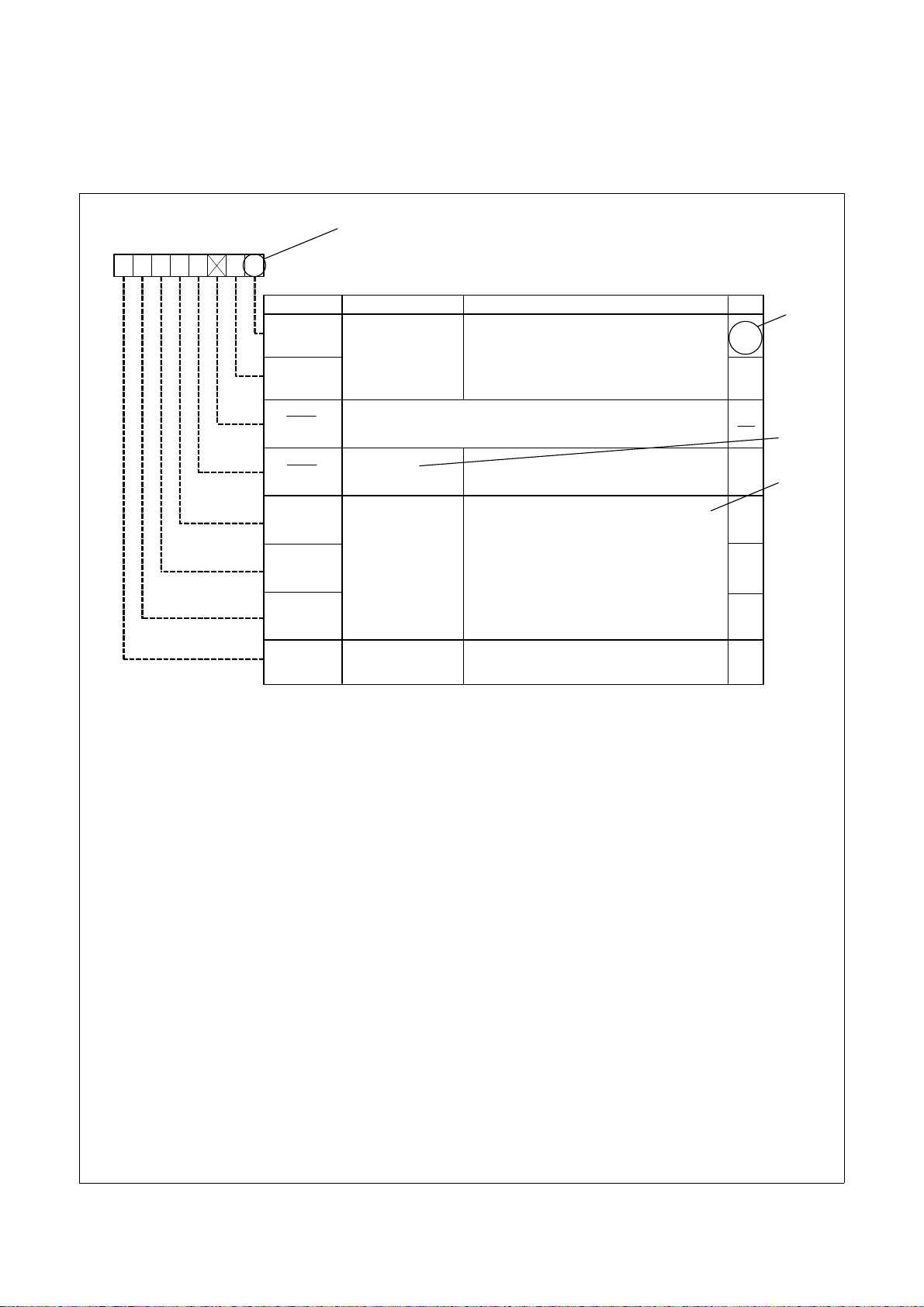
3. Register Notation
The symbols and terms used in register diagrams are described below.
XXX Register
b7 b6 b5 b4 b3 b2 b1 b0
0
XXX0
XXX1
(b2)
(b3)
XXX4
XXX5
XXX6
XXX7
*1
Symbol Address After Reset
XXX XXX 00h
Bit NameBit Symbol
XXX bits
Nothing is assigned. If necessary, set to 0.
When read, the content is undefined.
Reserved bits
XXX bits
XXX bit
b1 b0
1 0: XXX
0 1: XXX
1 0: Do not set.
1 1: XXX
Set to 0.
Function varies according to the operating
mode.
0: XXX
1: XXX
Function
RW
RW
RW
RW
RW
WO
RW
RO
*2
*3
*4
*1
Blank: Set to 0 or 1 according to the application.
0: Set to 0.
1: Set to 1.
X: Nothing is assigned.
*2
RW: Read and write.
RO: Read only.
WO: Write only.
−: Nothing is assigned.
*3
• Reserved bit
Reserved bit. Set to specified value.
*4
• Nothing is assigned
Nothing is assigned to the bit. As the bit may be used for future functions, if necessary, set to 0.
• Do not set to a value
Operation is not guaranteed when a value is set.
• Function varies according to the operating mode.
The function of the bit varies with the peripheral function mode. Refer to the register diagram for information
on the individual modes.
Page 7

4. List of Abbreviations and Acronyms
Abbreviation Full Form
ACIA Asynchronous Communication Interface Adapter
bps bits per second
CRC Cyclic Redundancy Check
DMA Direct Memory Access
DMAC Direct Memory Access Controller
GSM Global System for Mobile Communications
Hi-Z High Impedance
IEBus Inter Equipment bus
I/O Input/Output
IrDA Infrared Data Association
LSB Least Significant Bit
MSB Most Significant Bit
NC Non-Connection
PLL Phase Locked Loop
PWM Pulse Width Modulation
SFR Special Function Registers
SIM Subscriber Identity Module
UART Universal Asynchronous Receiver/Transmitter
VCO Voltage Controlled Oscillator
All trademarks and registered trademarks are the property of their respective owners.
Page 8

Table of Contents
SFR Page Reference ........................................................................................................................... B - 1
1. Overview ......................................................................................................................................... 1
1.1 Features ..................................................................................................................................................... 1
1.1.1 Applications .......................................................................................................................................... 1
1.1.2 Specifications ........................................................................................................................................ 2
1.2 Product List ............................................................................................................................................... 6
1.3 Block Diagram ........................................ .................................. .................................. ............................. 9
1.4 Pin Assignment ........................................................................................................................................ 10
1.5 Pin Functions ........................................................................................................................................... 13
2. Central Processing Unit (CPU) ..................................................................................................... 15
2.1 Data Registers (R0, R1, R2, and R3) ...................................................................................................... 16
2.2 Address Registers (A0 and A1) ............................................................................................................... 16
2.3 Frame Base Register (FB) ....................................................................................................................... 16
2.4 Interrupt Table Register (INTB) .............................................................................................................. 16
2.5 Program Counter (PC) ................................................................... ... ....................................................... 16
2.6 User Stack Pointer (USP) and Interrupt Stack Pointer (ISP) .................................................................. 16
2.7 Static Base Register (SB) ........................................................................................................................ 16
2.8 Flag Register (FLG) ................................................................................................................................ 16
2.8.1 Carry Flag (C) ..................................................................................................................................... 16
2.8.2 Debug Flag (D) ................................................................................................................................... 16
2.8.3 Zero Flag (Z) ....................................................................................................................................... 16
2.8.4 Sign Flag (S) ....................................................................................................................................... 16
2.8.5 Register Bank Select Flag (B) ............................................................................................................ 16
2.8.6 Overflow Flag (O) .............................................................................................................................. 16
2.8.7 Interrupt Enable Flag (I) ................................................................... .................................................. 17
2.8.8 Stack Pointer Select Flag (U) .............................................................................................................. 17
2.8.9 Processor Interrupt Priority Level (IPL) ........................................... .................................. ................ 17
2.8.10 Reserved Bit .............................. ................................................................. ......................................... 17
3. Memory ......................................................................................................................................... 18
3.1 R8C/2C Group ......................................................................................................................................... 18
3.2 R8C/2D Group ........................................................................................................................................ 19
4. Special Function Registers (SFRs) ............................................................................................... 20
5. Resets ........................................................................................................................................... 32
5.1 Hardware Reset ....................................................................................................................................... 35
5.1.1 When Power Supply is Stable .................................................................... ......................................... 35
5.1.2 Power On ............................................................................................................................................ 35
5.2 Power-On Reset Function ....................................................................................................................... 37
5.3 Voltage Monitor 0 Reset ......................................................................................................................... 38
5.4 Voltage Monitor 1 Reset ......................................................................................................................... 38
5.5 Voltage Monitor 2 Reset ......................................................................................................................... 38
5.6 Watchdog Timer Reset ............................................................................................................................ 39
5.7 Software Reset ......................................................................................................................................... 39
A - 1
Page 9

6. Voltage Detection Circuit .............................................................................................................. 40
6.1 VCC Input Voltage .................................................................................................................................. 47
6.1.1 Monitoring Vdet0 ............................................................ .................................. ................................. 47
6.1.2 Monitoring Vdet1 ............................................................ .................................. ................................. 47
6.1.3 Monitoring Vdet2 ............................................................ .................................. ................................. 47
6.2 Voltage Monitor 0 Reset ......................................................................................................................... 48
6.3 Voltage Monitor 1 Interrupt and Voltage Monitor 1 Reset ..................................................................... 49
6.4 Voltage Monitor 2 Interrupt and Voltage Monitor 2 Reset ..................................................................... 51
7. Programmable I/O Ports ............................................................................................................... 53
7.1 Functions of Programmable I/O Ports ..................................................................................................... 53
7.2 Effect on Peripheral Functions ................................................................................................................ 54
7.3 Pins Other than Programmable I/O Ports ................................................................................................ 54
7.4 Port settings ...................................... ................................. .................................. .................................... 71
7.5 Unassigned Pin Handling ........................................................................................................................ 92
8. Processor Mode ............................................................................................................................ 93
8.1 Processor Modes .................................... .................................. .................................. .............................. 93
9. Bus ................................................................................................................................................ 94
10. Clock Generation Circuit ............................................................................................................... 96
10.1 XIN Clock ..................................... .................................. ................................. ..................................... 106
10.2 On-Chip Oscillator Clocks .................................................................................................................... 107
10.2.1 Low-Speed On-Chip Oscillator Clock .............................................................................................. 107
10.2.2 High-Speed On-Chip Oscillator Clock ............................................................................................. 107
10.3 XCIN Clock ........................................................................................................................................... 108
10.4 CPU Clock and Peripheral Function Clock ........................................................................................... 109
10.4.1 System Clock ...................................................................................................................... .............. 109
10.4.2 CPU Clock ..................................................................................... .................................. ................. 109
10.4.3 Peripheral Function Clock (f1, f2, f4, f8, and f32) ........................................................................... 109
10.4.4 fOCO ................................................................................................................................................. 109
10.4.5 fOCO40M ......................................................................................................................................... 109
10.4.6 fOCO-F ............................................................................................................................................. 109
10.4.7 fOCO-S ............................................................................................................................................. 109
10.4.8 fOCO128 ........................................................................................................................................... 109
10.4.9 fC4 and fC32 .................................. .................................. ................................................................. 110
10.5 Power Control ........................................................................................................................................ 111
10.5.1 Standard Operating Mode ................................................................................................................. 111
10.5.2 Wait Mode .............................................. .................................. ........................................................ 113
10.5.3 Stop Mode ......................................................................................................................................... 117
10.6 Oscillation Stop Detection Function ..................................................................................................... 120
10.6.1 How to Use Oscillation Stop Detection Function ........................................... .................................. 120
10.7 Notes on Clock Generation Circuit ....................................................................................................... 123
10.7.1 Stop Mode ......................................................................................................................................... 123
10.7.2 Wait Mode .............................................. .................................. ........................................................ 123
10.7.3 Oscillation Stop Detection Function ................................................................................................. 123
10.7.4 Oscillation Circuit Constants ...................................................................................................... ...... 123
A - 2
Page 10

11. Protection .................................................................................................................................... 124
12. Interrupts ..................................................................................................................................... 125
12.1 Interrupt Overview ........................................................................................................................ ........ 125
12.1.1 Types of Interrupts ............................................................................................................................ 125
12.1.2 Software Interrupts ........................................................................................................................ ... 126
12.1.3 Special Interrupts ................................................................................................................ .............. 127
12.1.4 Peripheral Function Interrupt ............................................................................................................ 127
12.1.5 Interrupts and Interrupt Vectors ........................................................................................................ 128
12.1.6 Interrupt Control ............................................................................................................................... 130
12.2 INT
12.2.1 INTi
12.2.2 INTi
Interrupt ......................................................................................................................................... 139
Interrupt (i = 0 to 3) .................................................................................................................. 139
Input Filter (i = 0 to 3) ............................................ .................................. ............................... 142
12.3 Key Input Interrupt ................................................................................................................................ 143
12.4 Address Match Interrupt ........................... ............................................................................................. 145
12.5 Timer RC Interrupt, Timer RD Interrupt, Clock Synchronous Serial I/O with Chip Select Interrupts, and
2
I
C bus Interface Interrupt (Interrupts with Multiple Interrupt Request Sources) ................................ 147
12.6 Notes on Interrupts ................................................................................................................................ 149
12.6.1 Reading Address 00000h .................................................................................................................. 149
12.6.2 SP Setting .................................................................................................................................. ........ 149
12.6.3 External Interrupt and Key Input Interrupt ....................................................................................... 149
12.6.4 Changing Int e rrupt Sources .............................................................................................................. 150
12.6.5 Changing Interrupt Control Register Contents ................................................................................. 151
13. Watchdog Timer ......................................................................................................................... 152
13.1 Count Source Protection Mode Disabled .............................................................................................. 156
13.2 Count Source Protection Mode Enabled ............................................................................................... 157
14. Timers ......................................................................................................................................... 158
14.1 Timer RA ............................................................................................................................................... 161
14.1.1 Timer Mode ...................................................................................................................................... 164
14.1.2 Pulse Output Mode .................................................. ......................................................................... 166
14.1.3 Event Counter Mode ......................................................................................................................... 168
14.1.4 Pulse Width Measurement Mode ...................................................................................................... 170
14.1.5 Pulse Period Measurement Mode .......................................... ........................................................... 173
14.1.6 Notes on Timer RA ............................................................................................................. .............. 176
14.2 Timer RB ............................................................................................................................................... 177
14.2.1 Timer Mode ...................................................................................................................................... 181
14.2.2 Programmable Waveform Generation Mode .................................... ................................................ 184
14.2.3 Programmable One-shot Generation Mode ...................................................................................... 186
14.2.4 Programmable Wait One-Shot Generation Mode ............................................................................. 190
14.2.5 Notes on Timer RB ........................................................................................................................... 194
14.3 Timer RC ............................................................................................................................................... 198
14.3.1 Overview ........................................................................................................................................... 198
14.3.2 Registers Associated with Timer RC ................................................................................................ 200
14.3.3 Common Items for Multiple Modes ................................................................................................. 210
14.3.4 Timer Mode (Input Capture Function) ............................................................................................. 216
14.3.5 Timer Mode (Output Compare Function) ......................................................................................... 221
14.3.6 PWM Mode ......................... .................................. .................................. .................................. ........ 227
A - 3
Page 11

14.3.7 PWM2 Mode ................................................................................................................. .................... 232
14.3.8 Timer RC Interrupt ........................................................................................................................... 238
14.3.9 Notes on Timer RC ........................................................................................................................... 239
14.4 Timer RD ............................................................................................................................................... 240
14.4.1 Count Sources ................................................................................................................................... 245
14.4.2 Buffer Operation ............................................................................................................................... 246
14.4.3 Synchronous Operation ..................... .................................................................... ............................ 248
14.4.4 Pulse Output Forced Cutoff .............................................................................................................. 249
14.4.5 Input Capture Function ..................................................................................................................... 251
14.4.6 Output Compare Function ................................................................ ................................. ............... 266
14.4.7 PWM Mode ......................... .................................. .................................. .................................. ........ 284
14.4.8 Reset Synchronous PWM Mode ....................................................................................................... 298
14.4.9 Complementary PWM Mode ............................................................................................................ 309
14.4.10 PWM3 Mode ..................................................................................................................................... 324
14.4.11 Timer RD Interrupt ........................................................................................................................... 338
14.4.12 Notes on Timer RD ........................................................................................................................... 340
14.5 Timer RE ............................................................................................................................................... 346
14.5.1 Real-Time Clock Mode .................................................................................................................... 347
14.5.2 Output Compare Mode .................................................... .................................. ............................... 355
14.5.3 Notes on Timer RE ........................................................................................................................... 361
14.6 Timer RF ............................................................................................................................................... 364
14.6.1 Input Capture Mode .......................................................................................................................... 369
14.6.2 Output Compare Mode .................................................... .................................. ............................... 372
14.6.3 Notes on Timer RF ........................................................................................................................... 376
15. Serial Interface ............................................................................................................................ 377
15.1 Clock Synchronous Serial I/O Mode .............. ....................................................................................... 384
15.1.1 Polarity Select Function ................................................................................................................. ... 388
15.1.2 LSB First/MSB First Select Function ............................................................................................... 388
15.1.3 Continuous Receive Mode ................................................................................................................ 389
15.2 Clock Asynchronous Serial I/O (UART) Mode .......................................... .......................................... 390
15.2.1 Bit Rate .................................. .................................. .................................. ....................................... 395
15.3 Notes on Serial Interface ....................................................................................................................... 396
16. Clock Synchronous Serial Interface ............................................................................................ 397
16.1 Mode Selection ...................................................................................................................................... 397
16.2 Clock Synchronous Serial I/O with Chip Select (SSU) ........................................................................ 398
16.2.1 Transfer Clock ............................................................................................................ ...................... 407
16.2.2 SS Shift Register (SSTRSR) ....................................................................................................... ...... 409
16.2.3 Interrupt Requests ........................................... .................................. ............................... ................. 410
16.2.4 Communication Modes and Pin Functions .................................................................................... ... 411
16.2.5 Clock Synchronous Communication Mode ...................................................................................... 412
16.2.6 Operation in 4-Wire Bus Communication Mode .............................................................................. 419
16.2.7 SCS
Pin Control and Arbitration ...................................................................................................... 425
16.2.8 Notes on Clock Synchronous Serial I/O with Chip Select ............................................................... 426
16.3 I
2
C bus Interface ................................................................................................................................. ... 427
16.3.1 Transfer Clock ............................................................................................................ ...................... 437
16.3.2 Interrupt Requests ........................................... .................................. ............................... ................. 438
16.3.3 I
2
C bus Interface Mode ..................................................................................................................... 439
A - 4
Page 12

16.3.4 Clock Synchronous Serial Mode ...................................................................................................... 450
16.3.5 Examples of Register Setting ............................................................................................................ 453
16.3.6 Noise Canceller ............................................................................................................. .................... 457
16.3.7 Bit Synchronization Circuit .............................................................................................................. 458
16.3.8 Notes on I
2
C bus Interface ................................................................................................................ 459
17. Hardware LIN .............................................................................................................................. 460
17.1 Features ............................................................................................................................. .................... 460
17.2 I nput/Output Pins ................................................................................................................. ................. 461
17.3 Register Configuration .......................................................................................................................... 462
17.4 Functional Description .......................................................................................................................... 464
17.4.1 Master Mode ..................................................................................................................................... 464
17.4.2 Slave Mode ....................................................................................................................................... 467
17.4.3 Bus Collision Detection Function ..................................................................................................... 471
17.4.4 Hardware LIN End Processing ......................................................................................................... 472
17.5 I nterrupt Requests ......... .................................. ................................................................. ...................... 473
17.6 Notes on Hardware LIN ........................................................................................................................ 474
18. A/D Converter ............................................................................................................................. 475
18.1 Common Items for Multiple Modes ...................................................................................................... 480
18.1.1 Input/Output Pins .............................................................................................................................. 480
18.1.2 Sample and Hold .................................. .................................. ........................................................... 480
18.1.3 A/D Conversion Cycles ...................................................................................................... .............. 480
18.1.4 A/D Conversion Start Condition ..................... .................................................................................. 481
18.1.5 A/D Conversion Result ..................................................................................................................... 482
18.1.6 Low Current Consumption Function ................................................................................................ 482
18.2 One-Shot Mode ............................................................................................................................... ...... 483
18.3 Repeat Mode 0 ................................................................................................................................. ...... 484
18.4 Repeat Mode 1 ................................................................................................................................. ...... 485
18.5 S ingle Sweep Mode ..................................... .................................. ........................................................ 486
18.6 Repeat Sweep Mode .............................................................................................................................. 488
18.7 Internal Equivalent Circuit of Analog Input .......................................................................................... 490
18.8 Output Impedance of Sensor under A/D Conversion ............................................................................ 491
18.9 Notes on A/D Converter ........................................................................................................................ 492
19. D/A Converter ............................................................................................................................. 493
20. Flash Memory ............................................................................................................................. 495
20.1 Overview ................................................................................................................................. .............. 495
20.2 Memory Map ............................................... .......................................................................................... 496
20.3 Functions to Prevent Rewriting of Flash Memory ................................................................................ 498
20.3.1 ID Code Check Function ............................................................................................................... ... 498
20.3.2 ROM Code Protect Function ............................................................................................................ 499
20.4 CPU Rewrite Mode ........................................................... .................................. .................................. 500
20.4.1 EW0 Mode ........................................................................................................................................ 501
20.4.2 EW1 Mode ........................................................................................................................................ 501
20.4.3 Software Commands .............................................................................................................. ........... 510
20.4.4 Status Registers ........................................................................................................... ...................... 515
20.4.5 Full Status Check .............................................................................................................................. 516
A - 5
Page 13

20.5 Standard Serial I/O Mode ...................................................................................................................... 518
20.5.1 ID Code Check Function ............................................................................................................... ... 518
20.6 P arallel I/O Mode .................................................................................................................................. 522
20.6.1 ROM Code Protect Function ............................................................................................................ 522
20.7 Notes on Flash Memory ................................................................................................................ ........ 523
20.7.1 CPU Rewrite Mode ........................................................................ .................................. ................. 523
21. Electrical Characteristics ............................................................................................................ 526
22. Usage Notes ............................................................................................................................... 551
22.1 Notes on Clock Generation Circuit ....................................................................................................... 551
22.1.1 Stop Mode ......................................................................................................................................... 551
22.1.2 Wait Mode .............................................. .................................. ........................................................ 551
22.1.3 Oscillation Stop Detection Function ................................................................................................. 551
22.1.4 Oscillation Circuit Constants ...................................................................................................... ...... 551
22.2 Notes on Interrupts ................................................................................................................................ 552
22.2.1 Reading Address 00000h .................................................................................................................. 552
22.2.2 SP Setting .................................................................................................................................. ........ 552
22.2.3 External Interrupt and Key Input Interrupt ....................................................................................... 552
22.2.4 Changing Int e rrupt Sources .............................................................................................................. 553
22.2.5 Changing Interrupt Control Register Contents ................................................................................. 554
22.3 Notes on Timers .................................................................................................................................... 555
22.3.1 Notes on Timer RA ............................................................................................................. .............. 555
22.3.2 Notes on Timer RB ........................................................................................................................... 556
22.3.3 Notes on Timer RC ........................................................................................................................... 560
22.3.4 Notes on Timer RD ............................................................................................................. .............. 561
22.3.5 Notes on Timer RE ........................................................................................................................... 567
22.3.6 Notes on Timer RF ........................................................................................................................... 570
22.4 Notes on Serial Interface ....................................................................................................................... 571
22.5 Notes on Clock Synchronous Serial Interface ....................................................................................... 572
22.5.1 Notes on Clock Synchronous Serial I/O with Chip Select ............................................................... 572
22.5.2 Notes on I
2
C bus Interface ................................................................................................................ 572
22.6 Notes on Hardware LIN ........................................................................................................................ 573
22.7 Notes on A/D Converter ........................................................................................................................ 574
22.8 Notes on Flash Memory ................................................................................................................ ........ 575
22.8.1 CPU Rewrite Mode ........................................................................ .................................. ................. 575
22.9 Notes on Noise ........................................................................................................................... ........... 578
22.9.1 Inserting a Bypass Capacitor between VCC and VSS Pins as a Countermeasure against Noise and
Latch-up ............................................................................................................................................ 578
22.9.2 Countermeasures against Noise Error of Port Control Registers ..................................................... 578
23. Notes on On-Chip Debugger ...................................................................................................... 579
24. Notes on Emulator Debugger ..................................................................................................... 580
Appendix 1. Package Dimensions ........................................................................................................ 581
Appendix 2. Connection Examples between Serial Writer and On-Chip Debugging Emulator ............ 582
A - 6
Page 14

Appendix 3. Example of Oscillation Evaluation Circuit ......................................................................... 583
Index ..................................................................................................................................................... 584
A - 7
Page 15
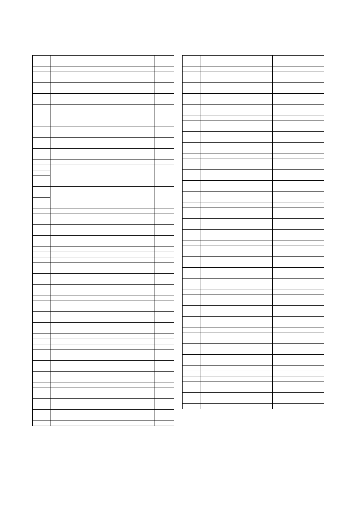
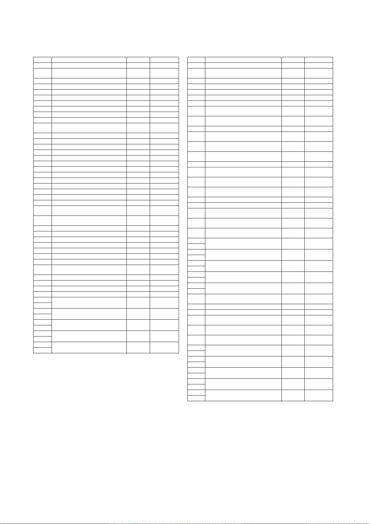
SFR Page Reference
Address Register Symbol Page
0000h
0001h
0002h
0003h
0004h Processor Mode Register 0 PM0 93
0005h Processor Mode Register 1 PM1 93
0006h System Clock Control Registe r 0 CM0 99
0007h System Clock Control Registe r 1 CM1 100
0008h Module Operation Enable Register MSTCR 201, 253,
0009h
000Ah Protect Register PRCR 124
000Bh
000Ch Oscillation Stop Detection Register OCD 101
000Dh Watchdog Timer Reset Register WDTR 154
000Eh Watchdog Timer Start Register WDTS 154
000Fh Watchdog Timer Control Register WDC 154
0010h Address Match Interrupt Register 0 RMAD0 146
0011h
0012h
0013h Address Match Interrupt Enable Register AIER 146
0014h Address Match Interrupt Register 1 RMAD1 146
0015h
0016h
0017h
0018h
0019h
001Ah
001Bh
001Ch Count Source Protection Mode Register CSPR 155
001Dh
001Eh
001Fh
0020h
0021h
0022h
0023h High-Speed On-Chip Oscillator Control Register 0 FRA0 102
0024h High-Speed On-Chip Oscillator Control Register 1 FRA1 102
0025h High-Speed On-Chip Oscillator Control Register 2 FRA2 103
0026h
0027h
0028h Clock Prescaler Reset Flag CPSRF 104
0029h
002Ah
002Bh High-Speed On-Chip Oscillator Control Register 6 FRA6 103
002Ch High-Speed On-Chip Oscillator Control Register 7 FRA7 103
002Dh
002Eh
002Fh
0030h
0031h Voltage Detection Register 1 VCA1 43
0032h Voltage Detection Register 2 VCA2 43, 104
0033h
0034h
0035h
0036h Voltage Monitor 1 Circuit Control Register VW1C 45
0037h Voltage Monitor 2 Circuit Control Register VW2C 46
0038h Voltage Monitor 0 Circuit Control Register VW0C 44
0039h
003Ah
003Bh
003Ch
003Dh
003Eh
003Fh
NOTE:
1. The blank regions are reserved. Do not access locations in these
268, 286,
300, 311,
326, 399,
regions.
429
Address Register Symbol Page
0040h
0041h
0042h
0043h
0044h
0045h
0046h
0047h Timer RC Interrupt Control Register TRCIC 131
0048h Timer RD0 Interrupt Control Register TRD0IC 131
0049h Timer RD1 Interrupt Control Register TRD1IC 131
004Ah Timer RE Interrupt Control Register TREIC 130
004Bh UART2 Transmit Interrupt Control Register S2TIC 130
004Ch UART2 Receive Interrupt Control Register S2RIC 130
004Dh Key Input Interrupt Control Register KUPIC 130
004Eh
004Fh SSU/IIC Interrupt Control Register SSUIC/IICIC 131
0050h Compare 1 Interrupt Control Register CMP1IC 130
0051h UART0 Transmit Interrupt Control Register S0TIC 130
0052h UART0 Receive Interrupt Control Register S0RIC 130
0053h UART1 Transmit Interrupt Control Register S1TIC 130
0054h UART1 Receive Interrupt Control Register S1RIC 130
0055h INT2 Interrupt Control Register INT2IC 132
0056h Timer RA Interrupt Control Register TRAIC 130
0057h
0058h Timer RB Interrupt Control Register TRBIC 130
0059h INT1 Interrupt Control Register INT1IC 132
005Ah INT3 Interrupt Control Register INT3IC 132
005Bh Timer RF Interrupt Control Register TRFIC 130
005Ch Compare 0 Interrupt Control Register CMP0IC 130
005Dh INT0 Interrupt Control Register INT0IC 132
005Eh A/D Conversion Interrupt Control Register ADIC 130
005Fh Capture Interrupt Control Register CAPIC 130
0060h
0061h
0062h
0063h
0064h
0065h
0066h
0067h
0068h
0069h
006Ah
006Bh
006Ch
006Dh
006Eh
006Fh
0070h
0071h
0072h
0073h
0074h
0075h
0076h
0077h
0078h
0079h
007Ah
007Bh
007Ch
007Dh
007Eh
007Fh
B - 1
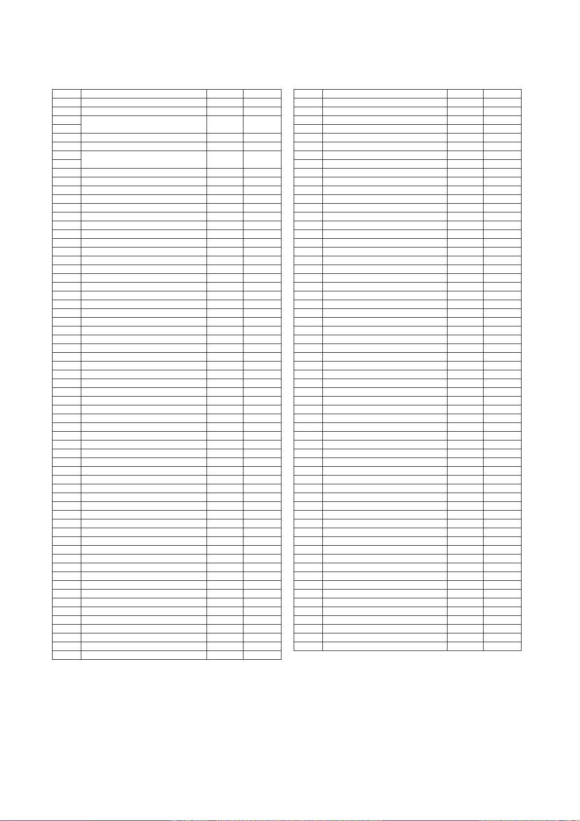
Page 16
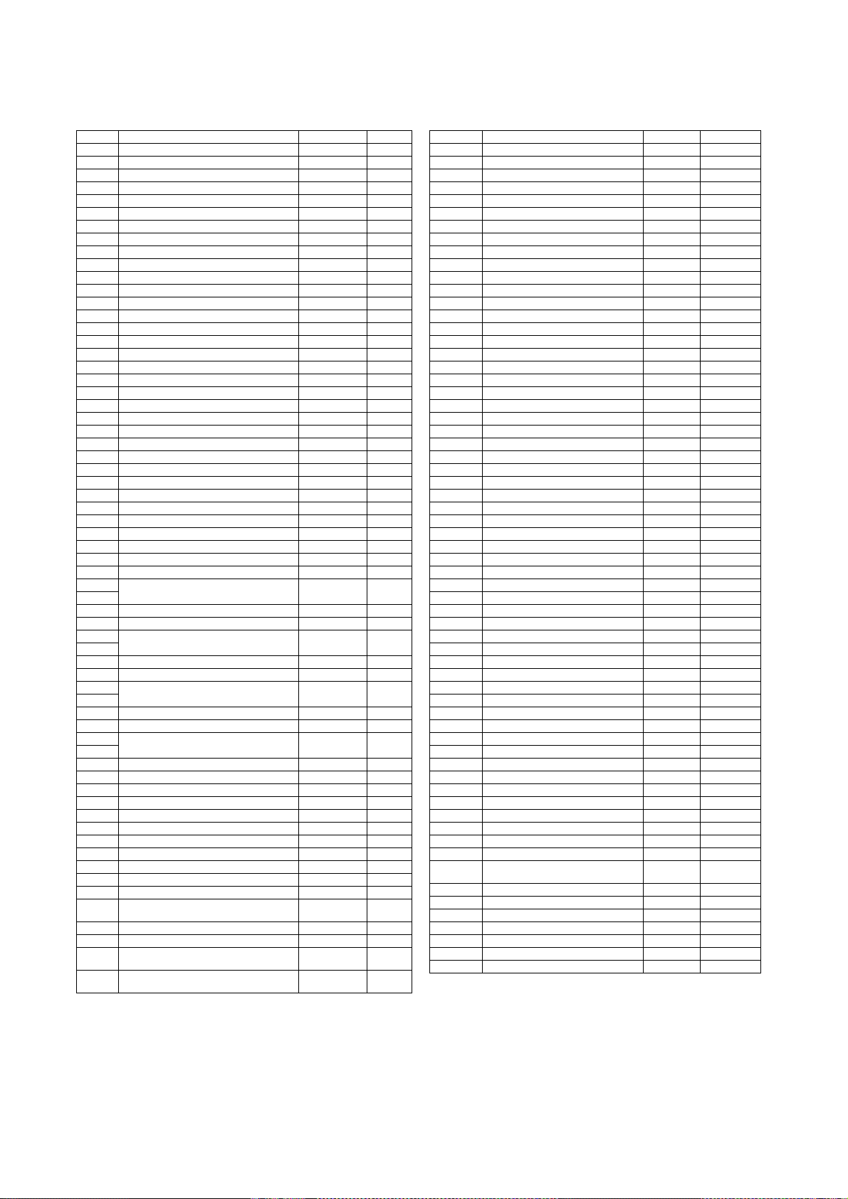
Address Register Symbol Page
0080h
0081h
0082h
0083h
0084h
0085h
0086h
0087h
0088h
0089h
008Ah
008Bh
008Ch
008Dh
008Eh
008Fh
0090h
0091h
0092h
0093h
0094h
0095h
0096h
0097h
0098h
0099h
009Ah
009Bh
009Ch
009Dh
009Eh
009Fh
00A0h UART0 Transmit/Receive Mode Register U0MR 380
00A1h UART0 Bit Rate Register U0BRG 380
00A2h UART0 Transmit Buffer Register U0TB 381
00A3h
00A4h UART0 Transmit / Receive Control Register 0 U0C0 381
00A5h UART0 Transmit / Receive Control Register 1 U0C1 382
00A6h UART0 Receive Buffer Register U0RB 382
00A7h
00A8h UART1 Transmit/Receive Mode Register U1MR 380
00A9h UART1 Bit Rate Register U1BRG 380
00AAh UART1 Transmit Buffer Register U1TB 381
00ABh
00ACh UART1 Transmit/Receive Control Register 0 U1C0 381
00ADh UART1 Transmit/Receive Control Register 1 U1C1 382
00AEh UART1 Receive Buffer Register U1RB 382
00AFh
00B0h
00B1h
00B2h
00B3h
00B4h
00B5h
00B6h
00B7h
SS Control Register H / IIC bus Control Register 1
00B8h
00B9h
SS Control Register L / IIC bus Control Register 2
00BAh SS Mode Register / IIC bus Mode Register SSMR/ICMR 402, 432
00BBh SS Enable Register / IIC bus Interr upt Enable
Register
00BCh SS Status Register / IIC bus Status Register SSSR/ICSR 404, 434
00BDh SS Mode Register 2 / Slave Address Register SSMR2/SAR 405, 435
00BEh SS Transmit Data Register/IIC Bus Transmit
Data Register
00BFh SS Receive Data Register/IIC Bus Receive
Data Register
SSCRH/ICCR1 400, 430
SSCRL/ICCR2 401, 431
SSER/ICIER 403, 433
SSTDR/ICDRT 406, 435
SSRDR/ICDRR 406, 436
NOTE:
1. The blank regions are reserved. Do not access locations in these
regions.
Address Register Symbol Page
00C0h
00C1h
00C2h
00C3h
00C4h
00C5h
00C6h
00C7h
00C8h
00C9h
00CAh
00CBh
00CCh
00CDh
00CEh
00CFh
00D0h
00D1h
00D2h
00D3h
00D4h
00D5h
00D6h
00D7h
00D8h D/A Register 0 DA0 494
00D9h
00DAh D/A Register 1 DA1 494
00DBh
00DCh D/A Control Register DACON 494
00DDh
00DEh
00DFh
00E0h Port P0 Register P0 68
00E1h Port P1 Register P1 68
00E2h Port P0 Direction Register PD0 67
00E3h Port P1 Direction Register PD1 67
00E4h Port P2 Register P2 68
00E5h Port P3 Register P3 68
00E6h Port P2 Direction Register PD2 67
00E7h Port P3 Direction Register PD3 67
00E8h Port P4 Register P4 68
00E9h Port P5 Register P5 68
00EAh Port P4 Direction Register PD4 67
00EBh Port P5 Direction Register PD5 67
00ECh Port P6 Register P6 68
00EDh
00EEh Port P6 Direction Register PD6 67
00EFh
00F0h
00F1h
00F2h
00F3h
00F4h Port P2 Drive Capacity Control Register P2DRR 69
00F5h UART1 Function Select Register U1SR 383
00F6h
00F7h
00F8h Port Mode Register PMR 69, 139, 383,
00F9h External Input Enable Register INTEN 140
00FAh INT Input Filter Select Register INTF 141
00FBh Key Input Enable Register KIEN 144
00FCh Pull-Up Control Register 0 PUR0 70
00FDh Pull-Up Control Register 1 PUR1 70
00FEh
00FFh
406, 436
B - 2
Page 17
Address Register Symbol Page
0100h Timer RA Control Register TRACR 162
0101h Timer RA I/O Control Register TRAIOC 162, 164, 167,
0102h Timer RA Mode Register TRAMR 163
0103h Timer RA Prescaler Register TRAPRE 163
0104h Timer RA Register TRA 163
0105h LIN Control Register 2 LINCR2 462
0106h LIN Control Register LINCR 462
0107h LIN Status Register LINST 463
0108h Timer RB Control Register TRBCR 178
0109h Timer RB One-Shot Control Register TRBOCR 178
010Ah Timer RB I/O Control Register TRBIOC 179, 181, 185,
010Bh Timer RB Mode Register TRBMR 179
010Ch Timer RB Prescaler Register TRBPRE 180
010Dh Timer RB Secondary Register TRBSC 180
010Eh Timer RB Primary Register TRBPR 180
010Fh
0110h
0111h
0112h
0113h
0114h
0115h
0116h
0117h
0118h Timer RE Second Data Register / Counter
Data Register
0119h Timer RE Minute Data Register / Compare
Data Register
011Ah Timer RE Hour Data Register TREHR 350
011Bh Timer RE Day of Week Data Register TREWK 350
011Ch Timer RE Control Register 1 TRECR1 351, 358
011Dh Timer RE Control Register 2 TRECR2 352, 358
011Eh Timer RE Clock Source Select Register TRECSR 353, 359
011Fh
0120h Timer RC Mode Register TRCMR 201
0121h Timer RC Control Register 1 TRCCR1 202, 225, 229,
0122h Timer RC Interrupt Enable Register TRCIER 203
0123h Timer RC Status Register TRCSR 204
0124h Timer RC I/O Control Register 0 TRCIOR0 209, 218, 223
0125h Timer RC I/O Control Register 1 TRCIOR1 209, 219, 224
0126h Timer RC Counter TRC 205
0127h
0128h Timer RC General Register A TRCGRA 205
0129h
012Ah Timer RC General Register B TRCGRB 205
012Bh
012Ch Timer RC General Register C TRCGRC 205
012Dh
012Eh Timer RC General Register D TRCGRD 205
012Fh
NOTE:
1. The blank regions are reserved. Do not access locations in these
regions.
TRESEC 349, 357
TREMIN 349, 357
169, 171, 174
187, 192
234
Address Register Symbol Page
0130h Timer RC Control Register 2 TRCCR2 206
0131h Timer RC Digital Filter Function Select
Register
0132h Timer RC Output Master Enable Register TRCOER 208
0133h
0134h
0135h
0136h
0137h Timer RD Start Register TRDSTR 254, 269, 287,
0138h Timer RD Mode Register TRDMR 254, 269, 287,
0139h Timer RD PWM Mode Register TRDPMR 255, 270, 288
013Ah Timer RD Function Control Register TRDFCR 256, 271, 289,
013Bh Timer RD Output Master En able Register 1 TRDOER1 272, 290, 303,
013Ch Timer RD Ou tput Master Enable Register 2 TRDOER2 2 72, 290, 303,
013Dh Timer RD Output Control Register TRDOCR 273, 291, 331
013Eh Timer RD Digital Filter Function Select
Register 0
013Fh Timer RD Digital Filter Function Select
Register 1
0140h Timer RD Control Register 0 TRDCR0 258, 274, 291,
0141h Timer RD I/O Control Register A0 TRDIORA0 259, 275
0142h Timer RD I/O Control Register C0 TRDIORC0 260, 276
0143h Timer RD Status Register 0 TRDSR0 261, 277, 292,
0144h Timer RD Interrupt Enable Register 0 TRDIER0 262, 278, 293,
0145h Timer RD PWM Mode Output Level Control
Register 0
0146h Timer RD Counter 0 TRD0 262, 279, 294,
0147h
0148h Timer RD General Register A0 TRDGRA0 263, 279, 295,
0149h
014Ah Timer RD General Register B0 TRDGRB0 263, 279, 295,
014Bh
014Ch Timer RD General Register C0 TRDGRC0 263, 279, 295,
014Dh
014Eh Timer RD General Register D0 TRDGRD0 263, 279, 295,
014Fh
0150h Timer RD Control Register 1 TRDCR1 258, 274, 291,
0151h Timer RD I/O Control Register A1 TRDIORA1 259, 275
0152h Timer RD I/O Control Register C1 TRDIORC1 260, 276
0153h Timer RD Status Register 1 TRDSR1 261, 277, 292,
0154h Timer RD Interrupt Enable Register 1 TRDIER1 262, 278, 293,
0155h Timer RD PWM Mode Output Level Control
Register 1
0156h Timer RD Counter 1 TRD1 262, 279, 294,
0157h
0158h Timer RD General Register A1 TRDGRA1 263, 279, 295,
0159h
015Ah Timer RD General Register B1 TRDGRB1 263, 279, 295,
015Bh
015Ch Timer RD General Register C1 TRDGRC1 263, 279, 295,
015Dh
015Eh Timer RD General Register D1 TRDGRD1 263, 279, 295,
015Fh
TRCDF 207
301, 312, 327
301, 313, 328
302, 314, 329
315, 330
315, 330
TRDDF0 257
TRDDF1 257
304, 316, 332
305, 317, 333
306, 318, 334
TRDPOCR0 294
306, 319, 334
307, 319, 335
307, 319, 335
307, 335
307, 319, 335
316
305, 317, 333
306, 318, 334
TRDPOCR1 294
319
307, 319, 335
307, 319, 335
307, 319, 335
307, 319, 335
B - 3
Page 18
Address Register Symbol Page
0160h UART2 Transmit/Receive Mode Register U2MR 380
0161h UART2 Bit Rate Register U2BRG 380
0162h UART2 Transmit Buffer Registe r U2TB 381
0163h
0164h UART2 Transmit/Receive Control Register 0 U2C0 381
0165h UART2 Transmit/Receive Control Register 1 U2C1 382
0166h UART2 Receive Buffer Register U2RB 382
0167h
0168h
0169h
016Ah
016Bh
016Ch
016Dh
016Eh
016Fh
0170h
0171h
0172h
0173h
0174h
0175h
0176h
0177h
0178h
0179h
017Ah
017Bh
017Ch
017Dh
017Eh
017Fh
0180h
0181h
0182h
0183h
0184h
0185h
0186h
0187h
0188h
0189h
018Ah
018Bh
018Ch
018Dh
018Eh
018Fh
0190h
0191h
0192h
0193h
0194h
0195h
0196h
0197h
0198h
0199h
019Ah
019Bh
019Ch
019Dh
019Eh
019Fh
NOTE:
1. The blank regions are reserved. Do not access locations in these
regions.
Address Register Symbol Page
01A0h
01A1h
01A2h
01A3h
01A4h
01A5h
01A6h
01A7h
01A8h
01A9h
01AAh
01ABh
01ACh
01ADh
01AEh
01AFh
01B0h
01B1h
01B2h
01B3h Flash Memory Control Register 4 FMR4 506
01B4h
01B5h Flash Memory Control Register 1 FMR1 505
01B6h
01B7h Flash Memory Control Register 0 FMR0 504
01B8h
01B9h
01BAh
01BBh
01BCh
01BDh
01BEh
01C0h
01C1h
01C2h
01C3h
01C4h
01C5h
01C6h
01C7h
01C8h
01C9h
01CAh
01CBh
01CCh
01CDh
01CEh
01CFh
01D0h
01D1h
01D2h
01D3h
01D4h
01D5h
01D6h
01D7h
01D8h
01D9h
01DAh
01DBh
01DCh
01DDh
01DEh
01DFh
B - 4
Page 19

Address Register Symbol Page
01E0h
01E1h
01E2h
01E3h
01E4h
01E5h
01E6h
01E7h
01E8h
01E9h
01EAh
01EBh
01ECh
01EDh
01EEh
01EFh
01F0h
01F1h
01F2h
01F3h
01F4h
01F5h
01F6h
01F7h
01F8h
01F9h
01FAh
01FBh
01FCh
01FDh
01FEh
01FFh
0200h
0201h
0202h
0203h
0204h
0205h
0206h
0207h
0208h
0209h
020Ah
020Bh
020Ch
020Dh
020Eh
020Fh
0210h
0211h
0212h
0213h
0214h
0215h
0216h
0217h
0218h
0219h
021Ah
021Bh
021Ch
021Dh
021Eh
021Fh
NOTE:
1. The blank regions are reserved. Do not access locations in these
regions.
Address Register Symbol Page
0220h
0221h
0222h
0223h
0224h
0225h
0226h
0227h
0228h
0229h
022Ah
022Bh
022Ch
022Dh
022Eh
022Fh
0230h
0231h
0232h
0233h
0234h
0235h
0236h
0237h
0238h
0239h
023Ah
023Bh
023Ch
023Dh
023Eh
023Fh
0240h
0241h
0242h
0243h
0244h
0245h
0246h
0247h
0248h
0249h
024Ah
024Bh
024Ch
024Dh
024Eh
024Fh
0250h
0251h
0252h
0253h
0254h
0255h
0256h
0257h
0258h
0259h
025Ah
025Bh
025Ch
025Dh
025Eh
025Fh
B - 5
Page 20

Address Register Symbol Page
0260h
0261h
0262h
0263h
0264h
0265h
0266h
0267h
0268h
0269h
026Ah
026Bh
026Ch
026Dh
026Eh
026Fh
0270h
0271h
0272h
0273h
0274h
0275h
0276h
0277h
0278h
0279h
027Ah
027Bh
027Ch
027Dh
027Eh
027Fh
0280h
0281h
0282h
0283h
0284h
0285h
0286h
0287h
0288h
0289h
028Ah
028Bh
028Ch
028Dh
028Eh
028Fh
0290h Timer RF Register TRF 366
0291h
0292h
0293h
0294h
0295h
0296h
0297h
0298h
0299h
029Ah Timer RF Control Register 0 TRFCR0 367
029Bh Timer RF Control Register 1 TRFCR1 368
029Ch Capture / Compare 0 Register TRFM0 366
029Dh
029Eh Compare 1 Register TRFM1 366
029Fh
NOTE:
1. The blank regions are reserved. Do not access locations in these
regions.
Address Register Symbol Page
02A0h
02A1h
02A2h
02A3h
02A4h
02A5h
02A6h
02A7h
02A8h
02A9h
02AAh
02ABh
02ACh
02ADh
02AEh
02AFh
02B0h
02B1h
02B2h
02B3h
02B4h
02B5h
02B6h
02B7h
02B8h
02B9h
02BAh
02BBh
02BCh
02BDh
02BEh
02BFh
02C0h A/D Register 0 AD0 477
02C1h
02C2h A/D Register 1 AD1 477
02C3h
02C4h A/D Register 2 AD2 477
02C5h
02C6h A/D Register 3 AD3 477
02C7h
02C8h
02C9h
02CAh
02CBh
02CCh
02CDh
02CEh
02CFh
02D0h
02D1h
02D2h
02D3h
02D4h A/D Control Register 2 ADCON2 477
02D5h
02D6h A/D Control Register 0 ADCON0 478
02D7h A/D Control Register 1 ADCON1 479
02D8h
02D9h
02DAh
02DBh
02DCh
02DDh
02DEh
02DFh
B - 6
Page 21

Address Register Symbol Page
02E0h Port P7 Direction Register PD7 67
02E1h
02E2h Port P7 Register P7 68
02E3h
02E4h Port P8 Direction Register PD8 67
02E5h Port P9 Direction Register PD9 67
02E6h Port P8 Register P8 68
02E7h Port P9 Register P9 68
02E8h
02E9h
02EAh
02EBh
02ECh
02EDh
02EEh
02EFh
02F0h
02F1h
02F2h
02F3h
02F4h
02F5h
02F6h
02F7h
02F8h
02F9h
02FAh
02FBh
02FCh Pull-Up Control Register 2 PUR2 70
02FDh
02FEh
02FFh Timer RF Output Control Register TRFOUT 368
FFFFh Option Function Select Register OFS 34, 155, 499
NOTE:
1. The blank regions are reserved. Do not access locations in these
regions.
B - 7
Page 22

R8C/2C Group, R8C/2D Group
REJ09B0339-0200
RENESAS MCU
1. Overview
1.1 Features
The R8C/2C Group and R8C/2D Group of single-chip MCUs incorporates the R8C/ Tiny Series CPU core,
employing sophisticated instructions for a high level of efficiency. With 1 Mbyte of address space, and it is capable
of executing instructions at high speed. In addition, the CPU core boasts a multiplier for high-speed operation
processing.
Power consumption is low, and the supported operating modes allow additional power control. These MCUs also
use an anti-noise configuration to reduce emissions of electromagnetic noise and are designed to withstand EMI.
Integration of many peripheral functions, including multifunction timer and serial interface, reduces the number of
system components.
Furthermore, the R8C/2D Group has on-chip data flash (1 KB × 2 blocks).
The difference between the R8C/2C Group and R8C/2D Group is only the presence or absence of data flash. Their
peripheral functions are the same.
1.1.1 Applications
Electronic household appliances, office equipment, audio equipment, consumer equipment, etc.
Rev.2.00
Dec 05, 2007
Rev.2.00 Dec 05, 2007 Page 1 of 585
REJ09B0339-0200
Page 23
R8C/2C Group, R8C/2D Group 1. Overview
1.1.2 Specifications
Tables 1.1 and 1.2 outlines the Specifications for R8C/2C Group and Tables 1.3 and 1.4 outlines the
Specifications for R8C/2D Group.
Table 1.1 Specifications for R8C/2C Group (1)
Item Function Specification
CPU Central processing
unit
Memory ROM, RAM Refer to Table 1.5 Product List for R8C/2C Group.
Power Supply
Voltage
Detection
I/O Ports Programmable I/O
Clock Clock generation
Interrupts • External: 5 sources, Internal: 23 sources, Software: 4 sources
Watchdog Timer 15 bits × 1 (with prescaler), reset start selectable
Timer Timer RA 8 bits × 1 (with 8-bit prescaler)
Voltage detection
circuit
ports
circuits
Timer RB 8 bits × 1 (with 8-bit prescaler)
Timer RC 16 bits × 1 (with 4 capture/compare registers)
Timer RD 16 bits × 2 (with 4 capture/compare registers)
Timer RE 8 bits × 1
Timer RF 16 bits × 1 (with capture/compare register pin and compare register pin)
R8C/Tiny series core
• Number of fundamental instructions: 89
• Minimum instruction execution time:
50 ns (f(XIN) = 20 MHz, VCC = 3.0 to 5.5 V)
100 ns (f(XIN) = 10 MHz, VCC = 2.7 to 5.5 V)
200 ns (f(XIN) = 5 MHz, VCC = 2.2 to 5.5 V)
• Multiplier: 16 bits × 16 bits → 32 bits
• Multiply-accumulate instruction: 16 bits × 16 bits + 32 bits → 32 bits
• Operation mode: Single-chip mode (address space: 1 Mbyte)
• Power-on reset
• Voltage detection 3
• Input-only: 2 pins
• CMOS I/O ports: 71, selectable pull-up resistor
• High current drive ports: 8
3 circuits: XIN clock oscillation circuit (with on-chip feedback resistor),
On-chip oscillator (high-speed, low-speed)
(high-speed on-chip oscillator has a frequency adjustment function),
XCIN clock oscillation circuit (32 kHz)
• Oscillation stop detection: XIN clock oscillation stop detection function
• Frequency divider circuit: Dividing selectable 1, 2, 4, 8, and 16
• Low power consumption modes:
Standard operating mode (high-speed clock, low-speed clock, high-speed
on-chip oscillator, low-speed on-chip oscillator), wait mode, stop mode
Real-time clock (timer RE)
• Priority levels: 7 levels
Timer mode (period timer), pulse output mode (output level inverted every
period), event counter mode, pulse width measurement mode, pulse period
measurement mode
Timer mode (period timer), programmable waveform generation mode (PWM
output), programmable one-shot generation mode, programmable wait oneshot generation mode
Timer mode (input capture function, output compare function), PWM mode
(output 3 pins), PWM2 mode (PWM output pin)
Timer mode (input capture function, output compare function), PWM mode
(output 6 pins), reset synchronous PWM mode (output three-phase
waveforms (6 pins), sawtooth wave modulation), complementary PWM mode
(output three-phase waveforms (6 pins), triangular wave modulation), PWM3
mode (PWM output 2 pins with fixed period)
Real-time clock mode (count seconds, minutes, hours, days of week), output
compare mode
Input capture mode, output compare mode
Rev.2.00 Dec 05, 2007 Page 2 of 585
REJ09B0339-0200
Page 24

R8C/2C Group, R8C/2D Group 1. Overview
Table 1.2 Specifications for R8C/2C Group (2)
Item Function Specification
Serial
Interface
Clock Synchronous Serial I/O with
Chip Select (SSU)
2
(1)
C bus
I
LIN Module Hardware LIN: 1 (timer RA, UART0)
A/D Converter 10-bit resolution × 20 channels, includes sample and hold function, with sweep
D/A Converter 8-bit resolution × 2 circuits
Flash Memory • Programming and erasure voltage: VCC = 2.7 to 5.5 V
Operating Frequency/Supply
Voltage
Current consumption 12 mA (VCC = 5.0 V, f(XIN) = 20 MHz)
Operating Ambient Temperature -20 to 85°C (N version)
Package 80-pin LQFP
NOTES:
1. I
2
2. Specify the D version if D version functions are to be used.
3. Please contact Renesas Technology sales offices for the Y version.
UART0, UART1,
Clock synchronous serial I/O/UART × 3
UART2
1 (shared with I2C-bus)
1 (shared with SSU)
mode
• Programming and erasure endurance: 100 times
• Program security: ROM code protect, ID code check
• Debug functions: On-chip debug, on-board flash rewrite function
f(XIN) = 20 MHz (VCC = 3.0 to 5.5 V)
f(XIN) = 10 MHz (VCC = 2.7 to 5.5 V)
f(XIN) = 5 MHz (VCC = 2.2 to 5.5 V)
5.5 mA (VCC = 3.0 V, f(XIN) = 10 MHz)
2.1 µA (VCC = 3.0 V, wait mode (f(XCIN) = 32 kHz))
0.65 µA (VCC = 3.0 V, stop mode)
-40 to 85°C (D version)
-20 to 105°C (Y version)
(2)
(3)
Package code: PLQP0080KB-A (previous code: 80P6Q-A)
C bus is a trademark of Koninklijke Philips Electronics N. V.
Rev.2.00 Dec 05, 2007 Page 3 of 585
REJ09B0339-0200
Page 25

R8C/2C Group, R8C/2D Group 1. Overview
Table 1.3 Specifications for R8C/2D Group (1)
Item Function Specification
CPU Central processing
unit
Memory ROM, RAM Refer to Table 1.6 Product List for R8C/2D Group.
Power Supply
Voltage
Detection
I/O Ports Programmable I/O
Clock Clock generation
Interrupts • External: 5 sources, Internal: 23 sources, Software: 4 sources
Watchdog Timer 15 bits × 1 (with prescaler), reset start selectable
Timer Timer RA 8 bits × 1 (with 8-bit prescaler)
Voltage detection
circuit
ports
circuits
Timer RB 8 bits × 1 (with 8-bit prescaler)
Timer RC 16 bits × 1 (with 4 capture/compare registers)
Timer RD 16 bits × 2 (with 4 capture/compare registers)
Timer RE 8 bits × 1
Timer RF 16 bits × 1 (with capture/compare register pin and compare register pin)
R8C/Tiny series core
• Number of fundamental instructions: 89
• Minimum instruction execution time:
50 ns (f(XIN) = 20 MHz, VCC = 3.0 to 5.5 V)
100 ns (f(XIN) = 10 MHz, VCC = 2.7 to 5.5 V)
200 ns (f(XIN) = 5 MHz, VCC = 2.2 to 5.5 V)
• Multiplier: 16 bits × 16 bits → 32 bits
• Multiply-accumulate instruction: 16 bits × 16 bits + 32 bits → 32 bits
• Operation mode: Single-chip mode (address space: 1 Mbyte)
• Power-on reset
• Voltage detection 3
• Input-only: 2 pins
• CMOS I/O ports: 71, selectable pull-up resistor
• High current drive ports: 8
3 circuits: XIN clock oscillation circuit (with on-chip feedback resistor),
On-chip oscillator (high-speed, low-speed)
(high-speed on-chip oscillator has a frequency adjustment function),
XCIN clock oscillation circuit (32 kHz)
• Oscillation stop detection: XIN clock oscillation stop detection function
• Frequency divider circuit: Dividing selectable 1, 2, 4, 8, and 16
• Low power consumption modes:
Standard operating mode (high-speed clock, low-speed clock, high-speed
on-chip oscillator, low-speed on-chip oscillator), wait mode, stop mode
Real-time clock (timer RE)
• Priority levels: 7 levels
Timer mode (period timer), pulse output mode (output level inverted every
period), event counter mode, pulse width measurement mode, pulse period
measurement mode
Timer mode (period timer), programmable waveform generation mode (PWM
output), programmable one-shot generation mode, programmable wait oneshot generation mode
Timer mode (input capture function, output compare function), PWM mode
(output 3 pins), PWM2 mode (PWM output pin)
Timer mode (input capture function, output compare function), PWM mode
(output 6 pins), reset synchronous PWM mode (output three-phase
waveforms (6 pins), sawtooth wave modulation), complementary PWM mode
(output three-phase waveforms (6 pins), triangular wave modulation), PWM3
mode (PWM output 2 pins with fixed period)
Real-time clock mode (count seconds, minutes, hours, days of week), output
compare mode
Input capture mode, output compare mode
Rev.2.00 Dec 05, 2007 Page 4 of 585
REJ09B0339-0200
Page 26
R8C/2C Group, R8C/2D Group 1. Overview
Table 1.4 Specifications for R8C/2D Group (2)
Item Function Specification
Serial
Interface
Clock Synchronous Serial I/O with
Chip Select (SSU)
2
(1)
C bus
I
LIN Module Hardware LIN: 1 (timer RA, UART0)
A/D Converter 10-bit resolution × 20 channels, includes sample and hold function, with sweep
D/A Converter 8-bit resolution × 2 circuits
Flash Memory • Programming and erasure voltage: VCC = 2.7 to 5.5 V
Operating Frequency/Supply
Voltage
Current consumption 12 mA (VCC = 5.0 V, f(XIN) = 20 MHz)
Operating Ambient Temperature -20 to 85°C (N version)
Package 80-pin LQFP
NOTES:
1. I2C bus is a trademark of Koninklijke Philips Electronics N. V.
2. Specify the D version if D version functions are to be used.
3. Please contact Renesas Technology sales offices for the Y version.
UART0, UART1,
UART2
Clock synchronous serial I/O/UART × 3
1 (shared with I2C-bus)
1 (shared with SSU)
mode
• Programming and erasure endurance: 10,000 times (data flash)
1,000 times (program ROM)
• Program security: ROM code protect, ID code check
• Debug functions: On-chip debug, on-board flash rewrite function
f(XIN) = 20 MHz (VCC = 3.0 to 5.5 V)
f(XIN) = 10 MHz (VCC = 2.7 to 5.5 V)
f(XIN) = 5 MHz (VCC = 2.2 to 5.5 V)
5.5 mA (VCC = 3.0 V, f(XIN) = 10 MHz)
2.1 µA (VCC = 3.0 V, wait mode (f(XCIN) = 32 kHz))
0.65 µA (VCC = 3.0 V, stop mode)
-40 to 85°C (D version)
-20 to 105°C (Y version)
(2)
(3)
Package code: PLQP0080KB-A (previous code: 80P6Q-A)
Rev.2.00 Dec 05, 2007 Page 5 of 585
REJ09B0339-0200
Page 27
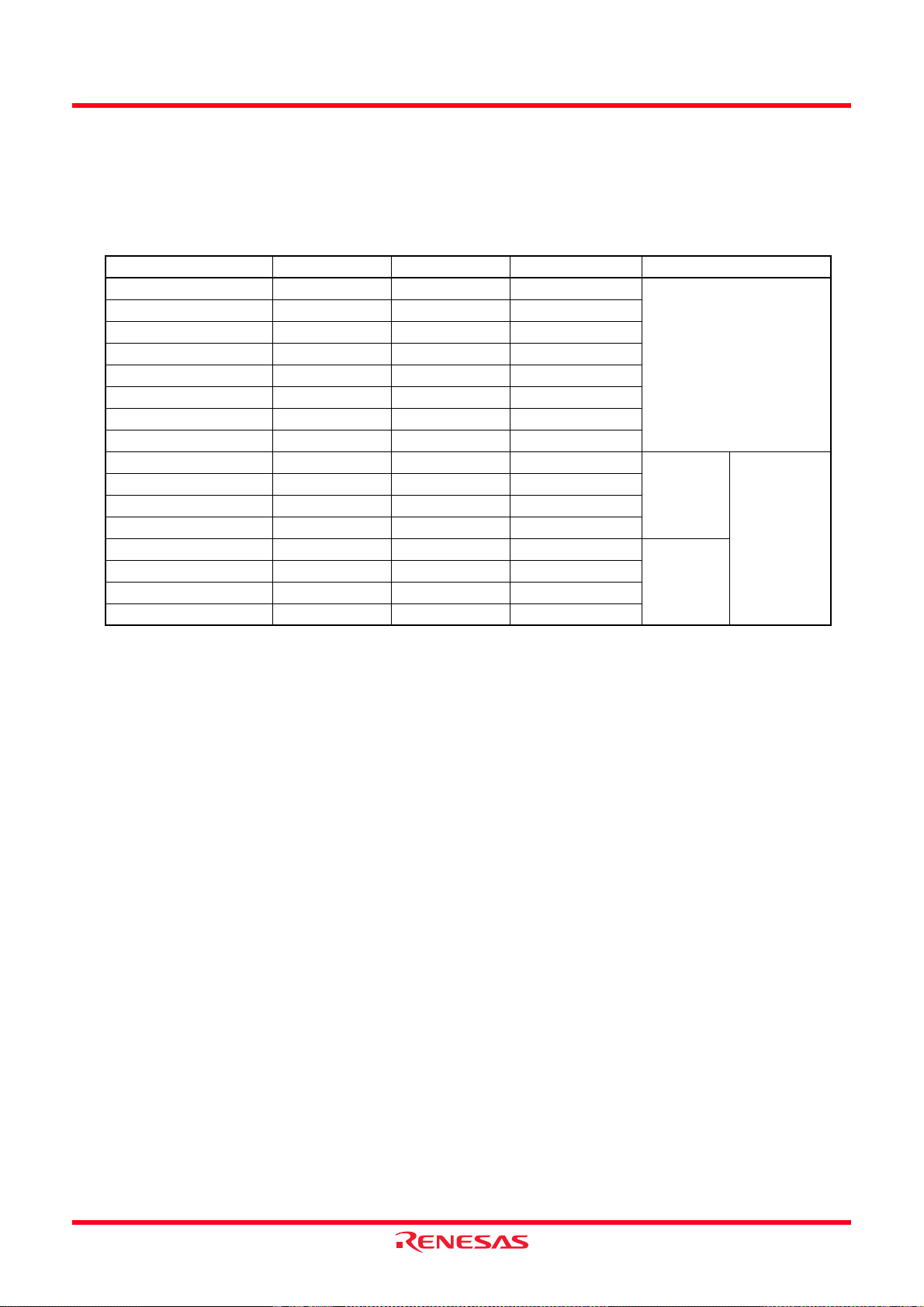
R8C/2C Group, R8C/2D Group 1. Overview
1.2 Product List
Table 1.5 lists Product List for R8C/2C Group, Figure 1.1 shows a Part Number, Memory Size, and Package of
R8C/2C Group, Table 1.6 lists Product List for R8C/2D Group, and Figure 1.2 shows a Part Number, Memory
Size, and Package of R8C/2D Group.
Table 1.5 Product List for R8C/2C Group Current of Dec. 2007
Part No. ROM Capacity RAM Capacity Package Type Remarks
R5F212C7SNFP 48 Kbytes 2.5 Kbytes PLQP0080KB-A N version
R5F212C8SNFP 64 Kbytes 3 Kbytes PLQP0080KB-A
R5F212CASNFP 96 Kbytes 7 Kbytes PLQP0080KB-A
R5F212CCSNFP 128 Kbytes 7.5 Kbytes PLQP0080KB-A
R5F212C7SDFP 48 Kbytes 2.5 Kbytes PLQP0080KB-A D version
R5F212C8SDFP 64 Kbytes 3 Kbytes PLQP0080KB-A
R5F212CASDFP 96 Kbytes 7 Kbytes PLQP0080KB-A
R5F212CCSDFP 128 Kbytes 7.5 Kbytes PLQP0080KB-A
R5F212C7SNXXXFP 48 Kbytes 2.5 Kbytes PLQP0080KB-A N version Factory
R5F212C8SNXXXFP 64 Kbytes 3 Kbytes PLQP0080KB-A
R5F212CASNXXXFP 96 Kbytes 7 Kbytes PLQP0080KB-A
R5F212CCSNXXXFP 128 Kbytes 7.5 Kbytes PLQP0080KB-A
R5F212C7SDXXXFP 48 Kbytes 2.5 Kbytes PLQP0080KB-A D version
R5F212C8SDXXXFP 64 Kbytes 3 Kbytes PLQP0080KB-A
R5F212CASDXXXFP 96 Kbytes 7 Kbytes PLQP0080KB-A
R5F212CCSDXXXFP 128 Kbytes 7.5 Kbytes PLQP0080KB-A
NOTE:
1. The user ROM is programmed before shipment.
programming
product
(1)
Rev.2.00 Dec 05, 2007 Page 6 of 585
REJ09B0339-0200
Page 28
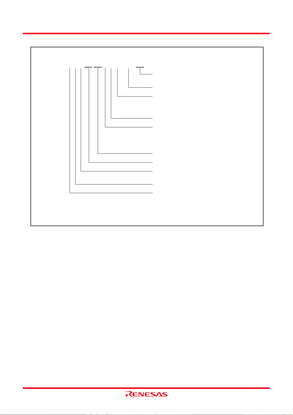
R8C/2C Group, R8C/2D Group 1. Overview
Part No. R 5 F 21 2C 7 S N XXX FP
Package type:
FP: PLQP0080KB-A (0.5 mm pin-pitch, 12 mm square body)
ROM number
Classification
N: Operating ambient temperature -20°C to 85°C
D: Operating ambient temperature -40°C to 85°C
Y: Operating ambient temperature -20°C to 105°C
S: Low-voltage version
ROM capacity
7: 48 KB
8: 64 KB
A: 96 KB
C: 128 KB
R8C/2C Group
R8C/Tiny Series
Memory type
F: Flash memory
(1)
Renesas MCU
Renesas semiconductor
NOTE:
1. Please contact Renesas Technology sales offices for the Y version.
Figure 1.1 Part Number, Memory Size, and Package of R8C/2C Group
Rev.2.00 Dec 05, 2007 Page 7 of 585
REJ09B0339-0200
Page 29
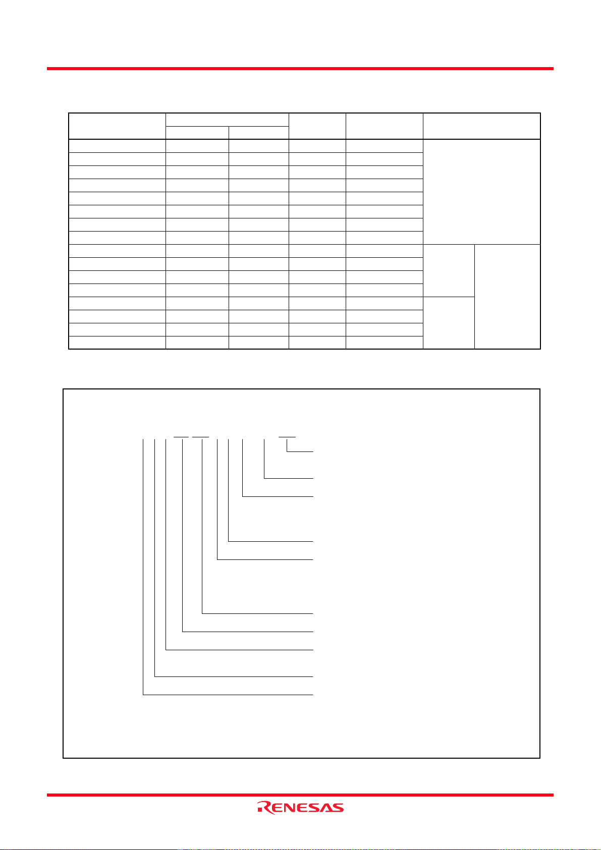
R8C/2C Group, R8C/2D Group 1. Overview
Table 1.6 Product List for R8C/2D Group Current of Dec. 2007
Part No.
ROM Capacity
Program ROM Data flash
R5F212D7SNFP 48 Kbytes 1 Kbyte × 2 2.5 Kbytes PLQP0080KB-A N version
R5F212D8SNFP 64 Kbytes 1 Kbyte × 2 3 Kbytes PLQP0080KB-A
R5F212DASNFP 96 Kbytes 1 Kbyte × 2 7 Kbytes PLQP0080KB-A
R5F212DCSNFP 128 Kbytes 1 Kbyte × 2 7.5 Kbytes PLQP0080KB-A
R5F212D7SDFP 48 Kbytes 1 Kbyte × 2 2.5 Kbytes PLQP0080KB-A D version
R5F212D8SDFP 64 Kbytes 1 Kbyte × 2 3 Kbytes PLQP0080KB-A
R5F212DASDFP 96 Kbytes 1 Kbyte × 2 7 Kbytes PLQP0080KB-A
R5F212DCSDFP 128 Kbytes 1 Kbyte × 2 7.5 Kbytes PLQP0080KB-A
R5F212D7SNXXXFP 48 Kbytes 1 Kbyte × 2 2.5 Kbytes PLQP0080KB-A N version
R5F212D8SNXXXFP 64 Kbytes 1 Kbyte × 2 3 Kbytes PLQP0080KB-A
R5F212DASNXXXFP 96 Kbytes 1 Kbyte × 2 7 Kbytes PLQP0080KB-A
R5F212DCSNXXXFP 128 Kbytes 1 Kbyte × 2 7.5 Kbytes PLQP0080KB-A
R5F212D7SDXXXFP 48 Kbytes 1 Kbyte × 2 2.5 Kbytes PLQP0080KB-A D version
R5F212D8SDXXXFP 64 Kbytes 1 Kbyte × 2 3 Kbytes PLQP0080KB-A
R5F212DASDXXXFP 96 Kbytes 1 Kbyte × 2 7 Kbytes PLQP0080KB-A
R5F212DCSDXXXFP 128 Kbytes 1 Kbyte × 2 7.5 Kbytes PLQP0080KB-A
RAM
Capacity
Package Type Remarks
Factory
programming
product
(1)
NOTE:
1. The user ROM is programmed before shipment.
Part No. R 5 F 21 2D 7 S N XXX FP
NOTE:
1. Please contact Renesas Technology sales offices for the Y version.
Package type:
FP: PLQP0080KB-A (0.5 mm pin-pitch, 12 mm square body)
ROM number
Classification
N: Operating ambient temperature -20°C to 85°C
D: Operating ambient temperature -40°C to 85°C
Y: Operating ambient temperature -20°C to 105°C
S: Low-voltage version
ROM capacity
7: 48 KB
8: 64 KB
A: 96 KB
C: 128 KB
R8C/2D Group
R8C/Tiny Series
Memory type
F: Flash memory
Renesas MCU
Renesas semiconductor
(1)
Figure 1.2 Part Number, Memory Size, and Package of R8C/2D Group
Rev.2.00 Dec 05, 2007 Page 8 of 585
REJ09B0339-0200
Page 30
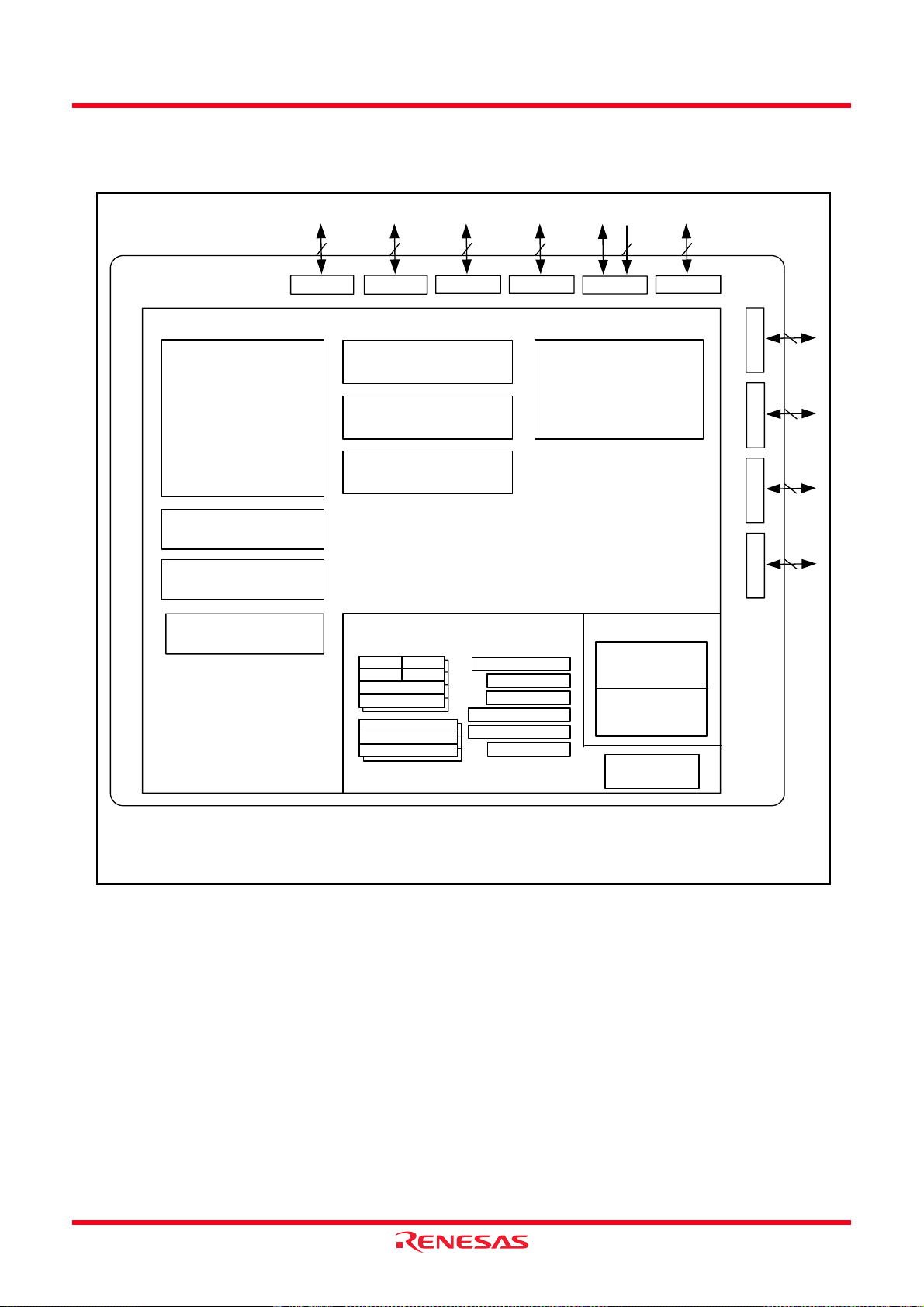
R8C/2C Group, R8C/2D Group 1. Overview
1.3 Block Diagram
Figure 1.3 shows a Block Diagram.
I/O ports
Peripheral functions
Timer RA (8 bits × 1)
Timer RB (8 bits × 1)
Timer RC (16 bits × 1)
Timer RD (16 bits × 2)
Timer RE (8 bits × 1)
Timer RF (16 bits × 1)
(10 bits
Timers
Watchdog timer
(15 bits)
A/D converter
× 20 channels)
D/A converter
(8 bits
× 2)
Port P0
8
8
Port P1
clock synchronous serial I/O
(8 bits × 3)
I2C bus or SSU
(8 bits × 1)
LIN module
Port P2
UART or
R8C/Tiny Series CPU core
R0H R0L
R1H
R1L
R2
R3
A0
A1
FB
8
8
Port P3
System clock generation
High-speed on-chip oscillator
Low-speed on-chip oscillator
3 2
Port P4
circuit
XIN-XOUT
XCIN-XCOUT
8
Port P5
Port P6
8
Port P7
8
Port P8
8
Port P9
4
Memory
SB
USP
ISP
INTB
PC
FLG
(1)
ROM
(2)
RAM
Multiplier
Figure 1.3 Block Diagram
Rev.2.00 Dec 05, 2007 Page 9 of 585
REJ09B0339-0200
NOTES:
1. ROM size varies with MCU type.
2. RAM size varies with MCU type.
Page 31

R8C/2C Group, R8C/2D Group 1. Overview
1.4 Pin Assignment
Figure 1.4 shows Pin Assignment (Top View). Tables 1.7 and 1.8 outlines the Pin Name Information by Pin
Number.
(2)
(2)
(2)
P7_4/AN16
P7_3/AN15
P7_2/AN14
P7_1/AN13
P7_0/AN12
P0_0/AN7
P0_1/AN6
P0_2/AN5
P0_3/AN4
P0_4/AN3
P6_2
P6_1
P0_5/AN2/CLK1
P0_6/AN1/DA0
VSS/AVSS
P0_7/AN0/DA1
VREF
VCC/AVCC
P3_7/SSO
P3_5/SCL/SSCK
P7_5/AN17
61
62
63
64
65
66
67
68
69
70
71
72
73
74
75
76
77
78
79
80
1 3456789101112131415162
P1_0/Kl0/AN8
P7_6/AN18
P7_7/AN19
P1_3/Kl3/AN11
P1_1/Kl1/AN9
P1_2/Kl2/AN10
R8C/2C Group
R8C/2D Group
PLQP0080KB-A(80P6Q-A)
P3_0/TRAO
P3_6/(INT1)
P3_2/(INT2)
52 51 50 49
(top view)
P3_1/TRBO
P6_3/TXD2
48 47 46 45 44 43 42 4160 59 58 57 56 55 54 53
P6_4/RXD2
P6_5/(CLK1)/CLK2
P6_7/INT3/RXD1
P6_6/INT2/TXD1
P8_0/TRFO00
P6_0/TREO
P4_5/INT0
17 18 19 20
P8_1/TRFO01
40
39
38
37
36
35
34
33
32
31
30
29
28
27
26
25
24
23
22
21
P8_2/TRFO02
P8_3/TRFO10/TRFI
P8_4/TRFO11
P8_5/TRFO12
P8_6
P8_7
P1_4/TXD0
P1_5/RXD0/(TRAIO)/(INT1)
P1_6/CLK0
P1_7/TRAIO/INT1
P2_0/TRDIOA0/TRDCLK
P2_1/TRDIOB0
P2_2/TRDIOC0
P2_3/TRDIOD0
P2_4/TRDIOA1
P2_5/TRDIOB1
P2_6/TRDIOC1
P2_7/TRDIOD1
P9_0
P9_1
(2)
P5_7
P5_6
P5_5
MODE
P3_3/SSI
P3_4/SDA/SCS
NOTES:
1. P4_7/XOUT are an input-only port.
2. Can be assigned to the pin in parentheses by a program.
3. Confirm the pin 1 position on the package by referring to the package dimensions.
Figure 1.4 Pin Assignment (Top View)
Rev.2.00 Dec 05, 2007 Page 10 of 585
REJ09B0339-0200
(1)
P9_3
RESET
P4_3/XCIN
P4_4/XCOUT
P4_6/XIN
VSS/AVSS
P4_7/XOUT
VCC/AVCC
P5_2/TRCIOB
P5_3/TRCIOC
P5_4/TRCIOD
P9_2
P5_0/TRCCLK
P5_1/TRCIOA/TRCTRG
Page 32

R8C/2C Group, R8C/2D Group 1. Overview
Table 1.7 Pin Name Information by Pin Number (1)
Pin
Number
Control Pin Port
Interrupt Timer
1 P3_3 SSI
2 P3_4
3 P5_7
4 P5_6
5 P5_5
6MODE
7 XCIN P4_3
8 XCOUT P4_4
9
RESET
10 XOUT P4_7
11 VSS/AVSS
12 XIN P4_6
13 VCC/AVCC
14 P5_4 TRCIOD
15 P5_3 TRCIOC
16 P5_2 TRCIOB
17 P5_1 TRCIOA/TRCTRG
18 P5_0 TRCCLK
19 P9_3
20 P9_2
21 P9_1
22 P9_0
23 P2_7 TRDIOD1
24 P2_6 TRDIOC1
25 P2_5 TRDIOB1
26 P2_4 TRDIOA1
27 P2_3 TRDIOD0
28 P2_2 TRDIOC0
29 P2_1 TRDIOB0
30 P2_0 TRDIOA0/ TRDCLK
31 P1_7
INT1
32 P1_6 CLK0
33 P1_5
(INT1
(1)
)
34 P1_4 TXD0
35 P8_7
36 P8_6
37 P8_5 TRFO12
38 P8_4 TRFO11
39 P8_3 TRFO10/TRFI
40 P8_2 TRFO02
41 P8_1 TRFO01
42 P8_0 TRFO00
43 P6_0 TREO
44 P4_5
45 P6_6
INT0
INT2
NOTE:
1. Can be assigned to the pin in parentheses by a program.
I/O Pin Functions for of Peripheral Modules
Serial
Interface
SSU
SCS
TRAIO
(TRAIO)
(1)
RXD0
INT0
TXD1
2
C bus
I
SDA
A/D Converter,
D/A Converter
Rev.2.00 Dec 05, 2007 Page 11 of 585
REJ09B0339-0200
Page 33

R8C/2C Group, R8C/2D Group 1. Overview
Table 1.8 Pin Name Information by Pin Number (2)
Pin
Number
46 P6_7
Control Pin Port
Interrupt Timer
INT3
47 P6_5
48 P6_4 RXD2
49 P6_3 TXD2
50 P3_1 TRBO
51 P3_0 TRAO
52 P3_6
53 P3_2
54 P1_3
55 P1_2
56 P1_1
57 P1_0
(INT1
(INT2
KI3
KI2
KI1
KI0
(1)
)
(1)
)
58 P7_7 AN19
59 P7_6 AN18
60 P7_5 AN17
61 P7_4 AN16
62 P7_3 AN15
63 P7_2 AN14
64 P7_1 AN13
65 P7_0 AN12
66 P0_0 AN7
67 P0_1 AN6
68 P0_2 AN5
69 P0_3 AN4
70 P0_4 AN3
71 P6_2
72 P6_1
73 P0_5 CLK1 AN2
74 P0_6 AN1/DA0
75 VSS/AVSS
76 P0_7 AN0/DA1
77 VREF
78 VCC/AVCC
79 P3_7 SSO
80 P3_5 SSCK SCL
NOTE:
1. Can be assigned to the pin in parentheses by a program.
I/O Pin Functions for of Peripheral Modules
Serial
Interface
SSU
2
C bus
I
RXD1
(1)
(CLK1)
/CLK2
A/D Converter,
D/A Converter
AN11
AN10
AN9
AN8
Rev.2.00 Dec 05, 2007 Page 12 of 585
REJ09B0339-0200
Page 34

R8C/2C Group, R8C/2D Group 1. Overview
1.5 Pin Functions
Tables 1.9 and 1.10 list Pin Functions.
Table 1.9 Pin Functions (1)
Item Pin Name
Power supply input VCC, VSS − Apply 2.2 V to 5.5 V to the VCC pin. Apply 0 V to the VSS pin.
Analog power
supply input
Reset input RESET
MODE MODE I Connect this pin to VCC via a resistor.
XIN clock input XIN I These pins are provided for XIN clock generation circuit I/O.
XIN clock output XOUT O
XCIN clock input XCIN I These pins are provided for XCIN clock generation circuit I/O.
XCIN clock output XCOUT O
INT interrupt input INT0 to INT3 IINT interrupt input pins.
Key input interrupt
Timer RA TRAIO I/O Timer RA I/O pin
Timer RB TRBO O Timer RB output pin
Timer RC TRCCLK I External clock input pin
Timer RD TRDIOA0, TRDIOA1,
Timer RE TREO O Divided clock output pin
Timer RF TRFI I Timer RF input pin
Serial interface CLK0, CLK1, CLK2 I/O Transfer clock I/O pins
2
I
C bus
SSU SSI I/O Data I/O pin
Reference voltage
input
I: Input O: Output I/O: Input and output
NOTE:
1. Refer to the oscillator manufacturer for oscillation characteristics.
AVCC, AVSS − Power supply for the A/D converter.
KI0 to KI3
TRAO O Timer RA output pin
TRCTRG I External trigger input pin
TRCIOA, TRCIOB,
TRCIOC, TRCIOD
TRDIOB0, TRDIOB1,
TRDIOC0, TRDIOC1,
TRDIOD0, TRDIOD1
TRDCLK I External clock input pin
TRFO00 to TRFO02,
TRFO10 to TRFO12
RXD0, RXD1, RXD2 I Serial data input pins
TXD0, TXD1, TXD2 O Serial data output pins
SCL I/O Clock I/O pin
SDA I/O Data I/O pin
SCS
SSCK I/O Clock I/O pin
SSO I/O Data I/O pin
VREF I Reference voltage input pin to A/D converter and D/A
I/O Type
Connect a capacitor between AVCC and AVSS.
I Input “L” on this pin resets the MCU.
Connect a ceramic resonator or a crystal oscillator between
the XIN and XOUT pins
to the XIN pin and leave the XOUT pin open.
Connect a crystal oscillator between the XCIN and XCOUT
(1)
pins
. To use an external clock, input it to the XCIN pin and
leave the XCOUT pin open.
INT0 is timer RD input pin. INT1 is timer RA input pin.
I Key input interrupt input pins
I/O Timer RC I/O pins
I/O Timer RD I/O pins
O Timer RF output pins
I/O Chip-select signal I/O pin
converter
Description
(1)
. To use an external clock, input it
Rev.2.00 Dec 05, 2007 Page 13 of 585
REJ09B0339-0200
Page 35

R8C/2C Group, R8C/2D Group 1. Overview
Table 1.10 Pin Functions (2)
Item Pin Name
A/D converter AN0 to AN19 I Analog input pins to A/D converter
D/A converter DA0 to DA1 O D/A converter output pins
I/O port P0_0 to P0_7,
P1_0 to P1_7,
P2_0 to P2_7,
P3_0 to P3_7,
P4_3 to P4_5,
P5_0 to P5_7,
P6_0 to P6_7,
P7_0 to P7_7,
P8_0 to P8_7,
P9_0 to P9_3
Input port P4_6, P4_7 I Input-only ports
I: Input O: Output I/O: Input and output
I/O Type
I/O CMOS I/O ports. Each port has an I/O select direction
register, allowing each pin in the port to be directed for input
or output individually.
Any port set to input can be set to use a pull-up resistor or not
by a program.
P2_0 to P2_7 also function as LED drive ports.
Description
Rev.2.00 Dec 05, 2007 Page 14 of 585
REJ09B0339-0200
Page 36

R8C/2C Group, R8C/2D Group 2. Central Processing Unit (CPU)
2. Central Processing Unit (CPU)
Figure 2.1 shows the CPU Registers. The CPU contains 13 registers. R0, R1, R2, R3, A0, A1, and FB configure a
register bank. There are two sets of register bank.
b31
R2
R3
b15 b8b7
R0H (high-order of R0)
R1H (high-order of R1)
R0L (low-order of R0)
R1L (low-order of R1)
R2
R3
A0
A1
FB
b15b19
INTBH
The 4 high order bits of INTB are INTBH and
the 16 low order bits of INTB are INTBL.
b19
INTBL
PC
b15
USP
ISP
SB
b0
Data registers
Address registers
Frame base register
b0
Interrupt table register
b0
Program counter
b0
User stack pointer
Interrupt stack pointer
Static base register
(1)
(1)
(1)
b15
IPL
NOTE:
1. These registers comprise a register bank. There are two register banks.
Figure 2.1 CPU Registers
b15
b0
FLG
b8
b7
b0
C
DZSBOIU
Flag register
Carry flag
Debug flag
Zero flag
Sign flag
Register bank select flag
Overflow flag
Interrupt enable flag
Stack pointer select flag
Reserved bit
Processor interrupt priority level
Reserved bit
Rev.2.00 Dec 05, 2007 Page 15 of 585
REJ09B0339-0200
Page 37

R8C/2C Group, R8C/2D Group 2. Central Processing Unit (CPU)
2.1 Data Registers (R0, R1, R2, and R3)
R0 is a 16-bit register for transfer, arithmetic, and logic operation s. The same applies to R1 to R3. R0 can be split
into high-order bits (R0H) and low-order bits (R0L) to be used separatel y as 8-bit data regi sters. R1H and R 1L are
analogous to R0H and R0L. R2 can be combined with R0 and used as a 32-bit data regi ster (R2R0). R3R1 is
analogous to R2R0.
2.2 Address Registers (A0 and A1)
A0 is a 16-bit register for address register indirect addressing and address register relative addressing. It is also
used for transfer, arithmetic, and logic operations. A1 is analogous to A0. A1 can be combined with A0 and as a 32bit address register (A1A0).
2.3 Frame Base Register (FB)
FB is a 16-bit register for FB relative addressing.
2.4 Interrupt Table Register (INTB)
INTB is a 20-bit register that indicates the start address of an interrupt vector table.
2.5 Program Counter (PC)
PC is 20 bits wide and indicates the address of the next instruction to be executed.
2.6 User Stack Pointer (USP) and Interrupt Stack Pointer (ISP)
The stack pointers (SP), USP, and ISP, are each 16 bits wide. The U flag of FLG is used to switch between
USP and ISP.
2.7 Static Base Register (SB)
SB is a 16-bit register for SB relative addressing.
2.8 Flag Register (FLG)
FLG is an 11-bit register indicating the CPU state.
2.8.1 Carry Flag (C)
The C flag retains carry, borrow, or shift-out bits that have been generated by the arithmetic and logic unit.
2.8.2 Debug Flag (D)
The D flag is for debugging only. Set it to 0.
2.8.3 Zero Flag (Z)
The Z flag is set to 1 when an arithmetic operation results in 0; otherwise to 0.
2.8.4 Sign Flag (S)
The S flag is set to 1 when an arithmetic operation results in a negative value; otherwise to 0.
2.8.5 Register Bank Select Flag (B)
Register bank 0 is selected when the B flag is 0. Register bank 1 is selected when this flag is set to 1.
2.8.6 Overflow Flag (O)
The O flag is set to 1 when an operation results in an overflow; otherwise to 0.
Rev.2.00 Dec 05, 2007 Page 16 of 585
REJ09B0339-0200
Page 38

R8C/2C Group, R8C/2D Group 2. Central Processing Unit (CPU)
2.8.7 Interrupt Enable Flag (I)
The I flag enables maskable interrupts.
Interrupt are disabled when the I flag is set to 0, and are enabled when the I flag is set to 1. The I flag is set to 0
when an interrupt request is acknowledged.
2.8.8 Stack Pointer Select Flag (U)
ISP is selected when the U flag is set to 0; USP is selected when the U flag is set to 1.
The U flag is set to 0 when a hardware interrupt request is acknowledged or the INT instruction of software
interrupt numbers 0 to 31 is executed.
2.8.9 Processor Interrupt Priority Level (IPL)
IPL is 3 bits wide and assigns processor interrupt priority levels from level 0 to level 7.
If a requested interrupt has higher priority than IPL, the interrupt is enabled.
2.8.10 Reserved Bit
If necessary, set to 0. When read, the content is undefined.
Rev.2.00 Dec 05, 2007 Page 17 of 585
REJ09B0339-0200
Page 39

R8C/2C Group, R8C/2D Group 3. Memory
3. Memory
3.1 R8C/2C Group
Figure 3.1 is a Memory Map of R8C/2C Group. The R8C/2C group has 1 Mbyte of address space from addresses
00000h to FFFFFh.
The internal ROM is allocated lower addresses, beginning with address 0FFFFh. For example, a 48-Kbyte internal
ROM area is allocated addresses 04000h to 0FFFFh.
The fixed interrupt vector table is allocated addresses 0FFDCh to 0FFFFh. They store the starting address of each
interrupt routine.
The internal RAM is allocated higher addresses, beginning with address 00400h. For example, a 2.5-Kbyte internal
RAM area is allocated addresses 00400h to 00DFFh. The internal RAM is used not only for storing data but also
for calling subroutines and as stacks when interrupt requests are acknowledged.
Special function registers (SFRs) are allocated addresses 00000h to 002FFh. The peripheral function control
registers are allocated here. All addresses within the SFR, which have nothing allocated are reserved for future use
and cannot be accessed by users.
00000h
002FFh
00400h
0XXXXh
03000h
0WWWWh
0YYYYh
0FFFFh
ZZZZZh
FFFFFh
NOTE:
1. The blank regions are reserved. Do not access locations in these regions.
SFR
(Refer to 4. Special
Function Registers
(SFRs))
Internal RAM
Internal RAM
Internal ROM
(program ROM)
Internal ROM
(program ROM)
Expanded area
0FFDCh
Watchdog timer, oscillation stop detection, voltage monitor
0FFFFh
Undefined instruction
Overflow
BRK instruction
Address match
Single step
(Reserved)
(Reserved)
Reset
Internal ROM Internal RAM
Size Address 0YYYYh
48 Kbytes
64 Kbytes
96 Kbytes
128 Kbytes
04000h
04000h
04000h
04000h
Address ZZZZZh Size
13FFFh
1BFFFh
23FFFh
Figure 3.1 Memory Map of R8C/2C Group
Rev.2.00 Dec 05, 2007 Page 18 of 585
REJ09B0339-0200
Address 0XXXXh
−
2.5 Kbytes
3 Kbytes
7 Kbytes
7.5 Kbytes
00DFFh
00FFFh
011FFh
011FFh
Address 0WWWWh
−
−
03DFFh
03FFFh
Page 40

R8C/2C Group, R8C/2D Group 3. Memory
3.2 R8C/2D Group
Figure 3.2 is a Memory Map of R8C/2D Group. The R8C/2D group has 1 Mbyte of address space from addresses
00000h to FFFFFh.
The internal ROM (program ROM) is allocated lower addresses, beginning with address 0FFFFh. For example, a
48-Kbyte internal ROM area is allocated addresses 04000h to 0FFFFh.
The fixed interrupt vector table is allocated addresses 0FFDCh to 0FFFFh. They store the starting address of each
interrupt routine.
The internal ROM (data flash) is allocated addresses 02400h to 02BFFh.
The internal RAM area is allocated higher addresses, beginning with address 00400h. For example, a 2.5-Kbyte
internal RAM is allocated addresses 00400h to 00DFFh. The internal RAM is used not only for storing data but
also for calling subroutines and as stacks when interrupt requests are acknowledged.
Special function registers (SFRs) are allocated addresses 00000h to 002FFh. The peripheral function control
registers are allocated here. All addresses within the SFR, which have nothing allocated are reserved for future use
and cannot be accessed by users.
00000h
002FFh
00400h
0XXXXh
02400h
02BFFh
03000h
0WWWWh
0YYYYh
0FFFFh
ZZZZZh
FFFFFh
NOTES:
1. Data flash block A (1 Kbyte) and B (1 Kbyte) are shown.
2. The blank regions are reserved. Do not access locations in these regions.
SFR
(Refer to 4. Special
Function Registers
(SFRs))
Internal RAM
Internal ROM
(data flash)
Internal RAM
Internal ROM
(program ROM)
Internal ROM
(program ROM)
Expanded area
(1)
0FFDCh
Watchdog timer, oscillation stop detection, voltage monitor
0FFFFh
Undefined instruction
Overflow
BRK instruction
Address match
Single step
(Reserved)
(Reserved)
Reset
Internal ROM Internal RAM
Size Address 0YYYYh
48 Kbytes
64 Kbytes
96 Kbytes
128 Kbytes
04000h
04000h
04000h
04000h
13FFFh
1BFFFh
23FFFh
Figure 3.2 Memory Map of R8C/2D Group
Rev.2.00 Dec 05, 2007 Page 19 of 585
REJ09B0339-0200
Address 0XXXXhAddress ZZZZZh Size
−
2.5 Kbytes
3 Kbytes
7 Kbytes
7.5 Kbytes
00DFFh
00FFFh
011FFh
011FFh
Address 0WWWWh
−
−
03DFFh
03FFFh
Page 41

R8C/2C Group, R8C/2D Group 4. Special Function Registers (SFRs)
4. Special Function Registers (SFRs)
An SFR (special function register) is a control register for a peripheral function. Tables 4.1 to 4.12 list the special
function registers.
Table 4.1 SFR Information (1)
Address Register Symbol After reset
0000h
0001h
0002h
0003h
0004h Processor Mode Register 0 PM0 00h
0005h Processor Mode Register 1 PM1 00h
0006h System Clock Control Register 0 CM0 01101000b
0007h System Clock Control Register 1 CM1 00100000b
0008h Module Operation Enable Register MSTCR 00h
0009h
000Ah Protect Register PRCR 00h
000Bh
000Ch Oscillation Stop Detection Register OCD 00000100b
000Dh Watchdog Timer Reset Register WDTR XXh
000Eh Watchdog Timer Start Register WDTS XXh
000Fh Watchdog Timer Control Register WDC 00X11111b
0010h Address Match Interrupt Register 0 RMAD0 00h
0011h 00h
0012h 00h
0013h Address Match Interrupt Enable Register AIER 00h
0014h Address Match Interrupt Register 1 RMAD1 00h
0015h 00h
0016h 00h
0017h
0018h
0019h
001Ah
001Bh
001Ch Count Source Protection Mode Register CSPR 00h
001Dh
001Eh
001Fh
0020h
0021h
0022h
0023h High-Speed On-Chip Oscillator Control Register 0 FRA0 00h
0024h High-Speed On-Chip Oscillator Control Register 1 FRA1 When shipping
0025h High-Speed On-Chip Oscillator Control Register 2 FRA2 00h
0026h
0027h
0028h Clock Prescaler Reset Flag CPSRF 00h
0029h
002Ah
002Bh High-Speed On-Chip Oscillator Control Register 6 FRA6 When Shipping
002Ch High-Speed On-Chip Oscillator Control Register 7 FRA7 When Shipping
(1)
10000000b
(6)
0030h
0031h
0032h
0033h
0034h
0035h
0036h
0037h
0038h
0039h
003Ah
003Eh
003Fh
X: Undefined
NOTES:
1. The blank regions are reserved. Do not access locations in these regions.
2. Software reset, watchdog timer reset, voltage monitor 1 reset, or voltage monitor 2 reset do not affect this register.
3. The LVD0ON bit in the OFS register is set to 1 and hardware reset.
4. Power-on reset, voltage monitor 0 reset, or the LVD0ON bit in the OFS register is set to 0 and hardware reset.
5. Software reset, watchdog timer reset, voltage monitor 1 reset, or voltage monitor 2 reset do not affect b2 and b3.
6. The CSPROINI bit in the OFS register is set to 0.
Voltage Detection Register 1
Voltage Detection Register 2
Voltage Monitor 1 Circuit Control Register
Voltage Monitor 2 Circuit Control Register
Voltage Monitor 0 Circuit Control Register
(2)
(2)
Rev.2.00 Dec 05, 2007 Page 20 of 585
REJ09B0339-0200
VCA1 00001000b
VCA2
(5)
(5)
(2)
VW1C 00001000b
VW2C 00h
VW0C
(3)
00h
00100000b
0000X000b
0100X001b
(4)
(3)
(4)
Page 42

R8C/2C Group, R8C/2D Group 4. Special Function Registers (SFRs)
Table 4.2 SFR Information (2)
Address Register Symbol After reset
0040h
0041h
0042h
0043h
0044h
0045h
0046h
0047h Timer RC Interrupt Control Register TRCIC XXXXX000b
0048h Timer RD0 Interrupt Control Register TRD0IC XXXXX000b
0049h Timer RD1 Interrupt Control Register TRD1IC XXXXX000b
004Ah Timer RE Interrupt Control Register TREIC XXXXX000b
004Bh UART2 Transmit Interrupt Control Register S2TIC XXXXX000b
004Ch UART2 Receive Interrupt Control Register S2RIC XXXXX000b
004Dh Key Input Interrupt Control Register KUPIC XXXXX000b
004Eh
004Fh
0050h Compare 1 Interrupt Control Register CMP1IC XXXXX000b
0051h UART0 Transmit Interrupt Control Register S0TIC XXXXX000b
0052h UART0 Receive Interrupt Control Register S0RIC XXXXX000b
0053h UART1 Transmit Interrupt Control Register S1TIC XXXXX000b
0054h UART1 Receive Interrupt Control Register S1RIC XXXXX000b
0055h INT2 Interrupt Control Register INT2IC XX00X000b
0056h Timer RA Interrupt Control Register TRAIC XXXXX000b
0057h
0058h Timer RB Interrupt Control Register TRBIC XXXXX000b
0059h INT1 Interrupt Control Register INT1IC XX00X000b
005Ah INT3 Interrupt Control Register INT3IC XX00X000b
005Bh Timer RF Interrupt Control Register TRFIC XXXXX000b
005Ch Compare 0 Interrupt Control Register CMP0IC XXXXX000b
005Dh INT0 Interrupt Control Register INT0IC XX00X000b
005Eh A/D Conversion Interrupt Control Register ADIC XXXXX000b
005Fh Capture Interrupt Control Register CAPIC XXXXX000b
0060h
0061h
0062h
0063h
0064h
0065h
0066h
0067h
0068h
0069h
006Ah
006Bh
006Ch
006Dh
006Eh
006Fh
0070h
0071h
0072h
0073h
0074h
0075h
0076h
0077h
0078h
0079h
007Ah
007Bh
007Ch
007Dh
007Eh
007Fh
X: Undefined
NOTES:
1. The blank regions are reserved. Do not access locations in these regions.
2. Selected by the IICSEL bit in the PMR register.
SSU/IIC Interrupt Control Register
(1)
(2)
SSUIC / IICIC XXXXX000b
Rev.2.00 Dec 05, 2007 Page 21 of 585
REJ09B0339-0200
Page 43

R8C/2C Group, R8C/2D Group 4. Special Function Registers (SFRs)
Table 4.3 SFR Information (3)
Address Register Symbol After reset
0080h
0081h
0082h
0083h
0084h
0085h
0086h
0087h
0088h
0089h
008Ah
008Bh
008Ch
008Dh
008Eh
008Fh
0090h
0091h
0092h
0093h
0094h
0095h
0096h
0097h
0098h
0099h
009Ah
009Bh
009Ch
009Dh
009Eh
009Fh
00A0h UART0 Transmit/Receive Mode Register U0MR 00h
00A1h UART0 Bit Rate Register U0BRG XXh
00A2h UART0 Transmit Buffer Register U0TB XXh
00A3h XXh
00A4h UART0 Transmit/Receive Control Register 0 U0C0 00001000b
00A5h UART0 Transmit/Receive Control Register 1 U0C1 00000010b
00A6h UART0 Receive Buffer Register U0RB XXh
00A7h XXh
00A8h UART1 Transmit/Receive Mode Register U1MR 00h
00A9h UART1 Bit Rate Register U1BRG XXh
00AAh UART1 Transmit Buffer Register U1TB XXh
00ABh XXh
00ACh UART1 Transmit/Receive Control Register 0 U1C0 00001000b
00ADh UART1 Transmit/Receive Control Register 1 U1C1 00000010b
00AEh UART1 Receive Buffer Register U1RB XXh
00AFh XXh
00B0h
00B1h
00B2h
00B3h
00B4h
00B5h
00B6h
00B7h
00B8h
00B9h
00BAh
00BBh
00BCh
00BDh
00BEh
00BFh
X: Undefined
NOTES:
1. The blank regions are reserved. Do not access locations in these regions.
2. Selected by the IICSEL bit in the PMR register.
SS Control Register H / IIC bus Control Register 1
SS Control Register L / IIC bus Control Register 2
SS Mode Register / IIC bus Mode Register
SS Enable Register / IIC bus Interrupt Enable Register
SS Status Register / IIC bus Status Register
SS Mode Register 2 / Slave Address Register
SS Transmit Data Register / IIC bus Transmit Data Register
SS Receive Data Register / IIC bus Receive Data Register
(1)
(2)
(2)
(2)
(2)
(2)
(2)
(2)
(2)
SSCRH / ICCR1 00h
SSCRL / ICCR2 01111101b
SSMR / ICMR 00011000b
SSER / ICIER 00h
SSSR / ICSR 00h / 0000X000b
SSMR2 / SAR 00h
SSTDR / ICDRT FFh
SSRDR / ICDRR FFh
Rev.2.00 Dec 05, 2007 Page 22 of 585
REJ09B0339-0200
Page 44

R8C/2C Group, R8C/2D Group 4. Special Function Registers (SFRs)
Table 4.4 SFR Information (4)
Address Register Symbol After reset
00C0h
00C1h
00C2h
00C3h
00C4h
00C5h
00C6h
00C7h
00C8h
00C9h
00CAh
00CBh
00CCh
00CDh
00CEh
00CFh
00D0h
00D1h
00D2h
00D3h
00D4h
00D5h
00D6h
00D7h
00D8h D/A Register 0 DA0 00h
00D9h
00DAh D/A Register 1 DA1 00h
00DBh
00DCh D/A Control Register DACON 00h
00DDh
00DEh
00DFh
00E0h Port P0 Register P0 XXh
00E1h Port P1 Register P1 XXh
00E2h Port P0 Direction Register PD0 00h
00E3h Port P1 Direction Register PD1 00h
00E4h Port P2 Register P2 XXh
00E5h Port P3 Register P3 XXh
00E6h Port P2 Direction Register PD2 00h
00E7h Port P3 Direction Register PD3 00h
00E8h Port P4 Register P4 XXh
00E9h Port P5 Register P5 XXh
00EAh Port P4 Direction Register PD4 00h
00EBh Port P5 Direction Register PD5 00h
00ECh Port P6 Register P6 XXh
00EDh
00EEh Port P6 Direction Register PD6 00h
00EFh
00F0h
00F1h
00F2h
00F3h
00F4h Port P2 Drive Capacity Control Register P2DRR 00h
00F5h UART1 Function Select Register U1SR 000000XXb
00F6h
00F7h
00F8h Port Mode Register PMR 00h
00F9h External Input Enable Register INTEN 00h
00FAh INT Input Filter Select Register INTF 00h
00FBh Key Input Enable Register KIEN 00h
00FCh Pull-Up Control Register 0 PUR0 00h
00FDh Pull-Up Control Register 1 PUR1 XX000000b
00FEh
00FFh
X: Undefined
NOTE:
1. The blank regions are reserved. Do not access locations in these regions.
(1)
Rev.2.00 Dec 05, 2007 Page 23 of 585
REJ09B0339-0200
Page 45

R8C/2C Group, R8C/2D Group 4. Special Function Registers (SFRs)
Table 4.5 SFR Information (5)
Address Register Symbol After reset
0100h Timer RA Control Register TRACR 00h
0101h Timer RA I/O Control Register TRAIOC 00h
0102h Timer RA Mode Register TRAMR 00h
0103h Timer RA Prescaler Register TRAPRE FFh
0104h Timer RA Register TRA FFh
0105h LIN Control Register 2 LINCR2 00h
0106h LIN Control Register LINCR 00h
0107h LIN Status Register LINST 00h
0108h Timer RB Control Register TRBCR 00h
0109h Timer RB One-Shot Control Register TRBOCR 00h
010Ah Timer RB I/O Control Register TRBIOC 00h
010Bh Timer RB Mode Register TRBMR 00h
010Ch Timer RB Prescaler Register TRBPRE FFh
010Dh Timer RB Secondary Register TRBSC FFh
010Eh Timer RB Primary Register TRBPR FFh
010Fh
0110h
0111h
0112h
0113h
0114h
0115h
0116h
0117h
0118h Timer RE Second Data Register / Counter Data Register TRESEC 00h
0119h Timer RE Minute Data Register / Compare Data Register TREMIN 00h
011Ah Timer RE Hour Data Register TREHR 00h
011Bh Timer RE Day of Week Data Register TREWK 00h
011Ch Timer RE Control Register 1 TRECR1 00h
011Dh Timer RE Control Register 2 TRECR2 00h
011Eh Timer RE Clock Source Select Register TRECSR 00001000b
011Fh
0120h Timer RC Mode Register TRCMR 01001000b
0121h Timer RC Control Register 1 TRCCR1 00h
0122h Timer RC Interrupt Enable Register TRCIER 01110000b
0123h Timer RC Status Register TRCSR 01110000b
0124h Timer RC I/O Control Register 0 TRCIOR0 10001000b
0125h Timer RC I/O Control Register 1 TRCIOR1 10001000b
0126h Timer RC Counter TRC 00h
0127h 00h
0128h Timer RC General Register A TRCGRA FFh
0129h FFh
012Ah Timer RC General Register B TRCGRB FFh
012Bh FFh
012Ch Timer RC General Register C TRCGRC FFh
012Dh FFh
012Eh Timer RC General Register D TRCGRD FFh
012Fh FFh
0130h Timer RC Control Register 2 TRCCR2 00011111b
0131h Timer RC Digital Filter Function Select Register TRCDF 00h
0132h Timer RC Output Master Enable Register TRCOER 01111111b
0133h
0134h
0135h
0136h
0137h Timer RD Start Register TRDSTR 11111100b
0138h Timer RD Mode Register TRDMR 00001110b
0139h Timer RD PWM Mode Register TRDPMR 10001000b
013Ah Timer RD Function Control Register TRDFCR 10000000b
013Bh Timer RD Output Master Enable Register 1 TRDOER1 FFh
013Ch Timer RD Output Master Enable Register 2 TRDOER2 01111111b
013Dh Timer RD Output Control Register TRDOCR 00h
013Eh Timer RD Digital Filter Function Select Register 0 TRDDF0 00h
013Fh Timer RD Digital Filter Function Select Register 1 TRDDF1 00h
NOTE:
1. The blank regions are reserved. Do not access locations in these regions
(1)
Rev.2.00 Dec 05, 2007 Page 24 of 585
REJ09B0339-0200
Page 46

R8C/2C Group, R8C/2D Group 4. Special Function Registers (SFRs)
Table 4.6 SFR Information (6)
Address Register Symbol After reset
0140h Timer RD Control Register 0 TRDCR0 00h
0141h Timer RD I/O Control Register A0 TRDIORA0 10001000b
0142h Timer RD I/O Control Register C0 TRDIORC0 10001000b
0143h Timer RD Status Register 0 TRDSR0 11000000b
0144h Timer RD Interrupt Enable Register 0 TRDIER0 11100000b
0145h Timer RD PWM Mode Output Level Control Register 0 TRDPOCR0 11111000b
0146h Timer RD Counter 0 TRD0 00h
0147h 00h
0148h Timer RD General Register A0 TRDGRA0 FFh
0149h FFh
014Ah Timer RD General Register B0 TRDGRB0 FFh
014Bh FFh
014Ch Timer RD General Register C0 TRDGRC0 FFh
014Dh FFh
014Eh Timer RD General Register D0 TRDGRD0 FFh
014Fh FFh
0150h Timer RD Control Register 1 TRDCR1 00h
0151h Timer RD I/O Control Register A1 TRDIORA1 10001000b
0152h Timer RD I/O Control Register C1 TRDIORC1 10001000b
0153h Timer RD Status Register 1 TRDSR1 11000000b
0154h Timer RD Interrupt Enable Register 1 TRDIER1 11100000b
0155h Timer RD PWM Mode Output Level Control Register 1 TRDPOCR1 11111000b
0156h Timer RD Counter 1 TRD1 00h
0157h 00h
0158h Timer RD General Register A1 TRDGRA1 FFh
0159h FFh
015Ah Timer RD General Register B1 TRDGRB1 FFh
015Bh FFh
015Ch Timer RD General Register C1 TRDGRC1 FFh
015Dh FFh
015Eh Timer RD General Register D1 TRDGRD1 FFh
015Fh FFh
0160h UART2 Transmit/Receive Mode Register U2MR 00h
0161h UART2 Bit Rate Register U2BRG XXh
0162h UART2 Transmit Buffer Register U2TB XXh
0163h XXh
0164h UART2 Transmit/Receive Control Register 0 U2C0 00001000b
0165h UART2 Transmit/Receive Control Register 1 U2C1 00000010b
0166h UART2 Receive Buffer Register U2RB XXh
0167h XXh
0168h
0169h
016Ah
016Bh
016Ch
016Dh
016Eh
016Fh
0170h
0171h
0172h
0173h
0174h
0175h
0176h
0177h
0178h
0179h
017Ah
017Bh
017Ch
017Dh
017Eh
017Fh
X: Undefined
NOTE:
1. The blank regions are reserved. Do not access locations in these regions.
(1)
Rev.2.00 Dec 05, 2007 Page 25 of 585
REJ09B0339-0200
Page 47

R8C/2C Group, R8C/2D Group 4. Special Function Registers (SFRs)
Table 4.7 SFR Information (7)
Address Register Symbol After reset
0180h
0181h
0182h
0183h
0184h
0185h
0186h
0187h
0188h
0189h
018Ah
018Bh
018Ch
018Dh
018Eh
018Fh
0190h
0191h
0192h
0193h
0194h
0195h
0196h
0197h
0198h
0199h
019Ah
019Bh
019Ch
019Dh
019Eh
019Fh
01A0h
01A1h
01A2h
01A3h
01A4h
01A5h
01A6h
01A7h
01A8h
01A9h
01AAh
01ABh
01ACh
01ADh
01AEh
01AFh
01B0h
01B1h
01B2h
01B3h Flash Memory Control Register 4 FMR4 01000000b
01B4h
01B5h Flash Memory Control Register 1 FMR1 1000000Xb
01B6h
01B7h Flash Memory Control Register 0 FMR0 00000001b
01B8h
01B9h
01BAh
01BBh
01BCh
01BDh
01BEh
01BFh
X: Undefined
NOTE:
1. The blank regions are reserved. Do not access locations in these regions.
(1)
Rev.2.00 Dec 05, 2007 Page 26 of 585
REJ09B0339-0200
Page 48

R8C/2C Group, R8C/2D Group 4. Special Function Registers (SFRs)
Table 4.8 SFR Information (8)
Address Register Symbol After reset
01C0h
01C1h
01C2h
01C3h
01C4h
01C5h
01C6h
01C7h
01C8h
01C9h
01CAh
01CBh
01CCh
01CDh
01CEh
01CFh
01D0h
01D1h
01D2h
01D3h
01D4h
01D5h
01D6h
01D7h
01D8h
01D9h
01DAh
01DBh
01DCh
01DDh
01DEh
01DFh
01E0h
01E1h
01E2h
01E3h
01E4h
01E5h
01E6h
01E7h
01E8h
01E9h
01EAh
01EBh
01ECh
01EDh
01EEh
01EFh
01F0h
01F1h
01F2h
01F3h
01F4h
01F5h
01F6h
01F7h
01F8h
01F9h
01FAh
01FBh
01FCh
01FDh
01FEh
01FFh
NOTE:
1. The blank regions are reserved. Do not access locations in these regions.
(1)
Rev.2.00 Dec 05, 2007 Page 27 of 585
REJ09B0339-0200
Page 49

R8C/2C Group, R8C/2D Group 4. Special Function Registers (SFRs)
Table 4.9 SFR Information (9)
Address Register Symbol After reset
0200h
0201h
0202h
0203h
0204h
0205h
0206h
0207h
0208h
0209h
020Ah
020Bh
020Ch
020Dh
020Eh
020Fh
0210h
0211h
0212h
0213h
0214h
0215h
0216h
0217h
0218h
0219h
021Ah
021Bh
021Ch
021Dh
021Eh
021Fh
0220h
0221h
0222h
0223h
0224h
0225h
0226h
0227h
0228h
0229h
022Ah
022Bh
022Ch
022Dh
022Eh
022Fh
0230h
0231h
0232h
0233h
0234h
0235h
0236h
0237h
0238h
0239h
023Ah
023Bh
023Ch
023Dh
023Eh
023Fh
NOTE:
1. The blank regions are reserved. Do not access locations in these regions.
(1)
Rev.2.00 Dec 05, 2007 Page 28 of 585
REJ09B0339-0200
Page 50

R8C/2C Group, R8C/2D Group 4. Special Function Registers (SFRs)
Table 4.10 SFR Information (10)
Address Register Symbol After reset
0240h
0241h
0242h
0243h
0244h
0245h
0246h
0247h
0248h
0249h
024Ah
024Bh
024Ch
024Dh
024Eh
024Fh
0250h
0251h
0252h
0253h
0254h
0255h
0256h
0257h
0258h
0259h
025Ah
025Bh
025Ch
025Dh
025Eh
025Fh
0260h
0261h
0262h
0263h
0264h
0265h
0266h
0267h
0268h
0269h
026Ah
026Bh
026Ch
026Dh
026Eh
026Fh
0270h
0271h
0272h
0273h
0274h
0275h
0276h
0277h
0278h
0279h
027Ah
027Bh
027Ch
027Dh
027Eh
027Fh
NOTE:
1. The blank regions are reserved. Do not access locations in these regions.
(1)
Rev.2.00 Dec 05, 2007 Page 29 of 585
REJ09B0339-0200
Page 51

R8C/2C Group, R8C/2D Group 4. Special Function Registers (SFRs)
Table 4.11 SFR Information (11)
Address Register Symbol After reset
0280h
0281h
0282h
0283h
0284h
0285h
0286h
0287h
0288h
0289h
028Ah
028Bh
028Ch
028Dh
028Eh
028Fh
0290h Timer RF Register TRF 00h
0291h 00h
0292h
0293h
0294h
0295h
0296h
0297h
0298h
0299h
029Ah Timer RF Control Register 0 TRFCR0 00h
029Bh Timer RF Control Register 1 TRFCR1 00h
029Ch
029Dh
029Eh Compare 1 Register TRFM1 FFh
029Fh FFh
02A0h
02A1h
02A2h
02A3h
02A4h
02A5h
02A6h
02A7h
02A8h
02A9h
02AAh
02ABh
02ACh
02ADh
02AEh
02AFh
02B0h
02B1h
02B2h
02B3h
02B4h
02B5h
02B6h
02B7h
02B8h
02B9h
02BAh
02BBh
02BCh
02BDh
02BEh
02BFh
NOTES:
1. The blank regions are reserved. Do not access locations in these regions.
2. After input capture mode.
3. After output compare mode.
Capture / Compare 0 Register TRFM0
(1)
0000h
FFFFh
(2)
(3)
Rev.2.00 Dec 05, 2007 Page 30 of 585
REJ09B0339-0200
Page 52

R8C/2C Group, R8C/2D Group 4. Special Function Registers (SFRs)
Table 4.12 SFR Information (12)
Address Register Symbol After reset
02C0h A/D Register 0 AD0 XXh
02C1h XXh
02C2h A/D Register 1 AD1 XXh
02C3h XXh
02C4h A/D Register 2 AD2 XXh
02C5h XXh
02C6h A/D Register 3 AD3 XXh
02C7h XXh
02C8h
02C9h
02CAh
02CBh
02CCh
02CDh
02CEh
02CFh
02D0h
02D1h
02D2h
02D3h
02D4h A/D Control Register 2 ADCON2 00001000b
02D5h
02D6h A/D Control Register 0 ADCON0 00000011b
02D7h A/D Control Register 1 ADCON1 00h
02D8h
02D9h
02DAh
02DBh
02DCh
02DDh
02DEh
02DFh
02E0h Port P7 Direction Register PD7 00h
02E1h
02E2h Port P7 Register P7 XXh
02E3h
02E4h Port P8 Direction Register PD8 00h
02E5h Port P9 Direction Register PD9 X0h
02E6h Port P8 Register P8 XXh
02E7h Port P9 Register P9 XXh
02E8h
02E9h
02EAh
02EBh
02ECh
02EDh
02EEh
02EFh
02F0h
02F1h
02F2h
02F3h
02F4h
02F5h
02F6h
02F7h
02F8h
02F9h
02FAh
02FBh
02FCh Pull-Up Control Register 2 PUR2 XXX00000b
02FDh
02FEh
02FFh Timer RF Output Control Register TRFOUT 00h
(1)
FFFFh Option Function Select Register OFS (Note 2)
X: Undefined
NOTES:
1. The blank regions are reserved. Do not access locations in these regions.
2. The OFS register cannot be changed by a program. Use a flash programmer to write to it.
Rev.2.00 Dec 05, 2007 Page 31 of 585
REJ09B0339-0200
Page 53

R8C/2C Group, R8C/2D Group 5. Resets
5. Resets
The following resets are implemented: hardware reset, power-on reset, voltage monitor 0 reset, voltage monitor 1
reset, voltage monitor 2 reset, watchdog timer reset, and software reset.
Table 5.1 lists the Reset Names and Sources.
Table 5.1 Reset Names and Sources
Reset Name Source
Hardware reset Input voltage of RESET
Power-on reset VCC rises
Voltage monitor 0 reset VCC falls (monitor voltage: Vdet0)
Voltage monitor 1 reset VCC falls (monitor voltage: Vdet1)
Voltage monitor 2 reset VCC falls (monitor voltage: Vdet2)
Watchdog timer reset Underflow of watchdog timer
Software reset Write 1 to PM03 bit in PM0 register
pin is held “L”
RESET
VCC
Power-on reset
circuit
Voltage
detection
circuit
Watchdog
timer
CPU
Hardware reset
Power-on reset
Voltage monitor 0 reset
Voltage monitor 1 reset
Voltage monitor 2
reset
Watchdog timer
reset
Software reset
VCA13: Bit in VCA1 register
VCA25, VCA26, VCA27: Bits in VCA2 register
VW0C0, VW0C1, VW0C6, VW0F0, VW0F1, VW0C7: Bits in VW0C register
VW1C2, VW1C3: Bits in VW1C register
VW2C2, VW2C3: Bits in VW2C register
SFRs
Bits VCA25,
VW0C0, and
VW0C6
SFRs
Bits VCA25,
VW0C0, and
VW0C6
SFRs
Bits VCA13, VCA26, VCA27,
VW1C2, VW1C3,
VW2C2, VW2C3,
VW0C1, VW0F0,
VW0F1, and VW0C7
Pin, CPU, and
SFR bits other than
those listed above
Figure 5.1 Block Diagram of Reset Circuit
Rev.2.00 Dec 05, 2007 Page 32 of 585
REJ09B0339-0200
Page 54

R8C/2C Group, R8C/2D Group 5. Resets
Table 5.2 shows the Pin Functions while RESET Pin Level is “L”, Figure 5.2 shows the CPU Register Status after
Reset, Figure 5.3 shows the Reset Sequence, and Figure 5.4 shows the OFS Register.
Table 5.2 Pin Functions while RESET
Pin Level is “L”
Pin Name Pin Functions
P0 to P3, P5 to P8 Input port
P4_3 to P4_7 Input port
P9_0 to P9_3 Input port
b15
b15
0000h
0000h
0000h
0000h
0000h
0000h
0000h
b19
00000h
Content of addresses 0FFFEh to 0FFFCh
b15
0000h
0000h
0000h
b15
0000h
b8
b7
b0
Data register(R0)
Data register(R1)
Data register(R2)
Data register(R3)
Address register(A0)
Address register(A1)
Frame base register(FB)
b0
Interrupt table register(INTB)
Program counter(PC)
b0
User stack pointer(USP)
Interrupt stack pointer(ISP)
Static base register(SB)
b0
Flag register(FLG)
b0
IPL
Figure 5.2 CPU Register Status after Reset
Rev.2.00 Dec 05, 2007 Page 33 of 585
REJ09B0339-0200
C
DZSBOIU
Page 55

R8C/2C Group, R8C/2D Group 5. Resets
fOCO-S
RESET pin
Internal reset
signal
CPU clock
Address
(internal address
signal)
NOTES:
1. Hardware reset.
2. When the “L” input width to the RESET pin is set to fOCO-S clock × 32 cycles or more, setting the RESET pin to “H” also sets the internal
10 cycles or more are needed
fOCO-S clock × 32 cycles
Start time of flash memory
(CPU clock × 14 cycles)
reset signal to “H” at the same.
(1)
(2)
CPU clock × 28 cycles
Figure 5.3 Reset Sequence
Option Function Select Register
b7 b6 b5 b4 b3 b2 b1 b0
111
NOTES:
The OFS register is on the flash memory. Write to the OFS register w ith a program. Af ter w riting is completed, do not
1.
w rite additions to the OFS register.
2.
To use the pow er-on reset, set the LV D0ON bit to 0 (voltage monitor 0 reset enabled after hardw are reset).
3. If the block including the OFS register is erased, FFh is set to the OFS register.
Symbol Addres s When Shipping
OFS
Bit Symbol Bit Name Function RW
WDTON RW
—
(b1)
ROMCR
ROMCP1
—
(b4)
LVD0ON
—
(b6)
CSPROINI
(1)
0FFFFh FFh
Watchdog timer start
select bit
0 : Starts w atchdog timer automatically af ter reset
1 : Watchdog timer is inactive af ter reset
Reserved bit Set to 1.
ROM code protect
disabled bit
0 : ROM c ode protect disabled
1 : ROMCP1 enabled
ROM code protect bit 0 : ROM code protect enabled
1 : ROM c ode protect disabled
Reserved bit Set to 1.
Voltage detection 0
circuit start bit
(2)
0 : Voltage monitor 0 reset enabled after hardw are
res et
1 : Voltage monitor 0 reset disabled after hardw are
res et
Reserved bit Set to 1.
Count source protect
mode after reset select
0 : Count source protect mode enabled after reset
1 : Count sourc e protec t mode disabled after reset
bit
0FFFCh 0FFFEh
0FFFDh
(3)
Content of reset vector
RW
RW
RW
RW
RW
RW
RW
Figure 5.4 OFS Register
Rev.2.00 Dec 05, 2007 Page 34 of 585
REJ09B0339-0200
Page 56

R8C/2C Group, R8C/2D Group 5. Resets
5.1 Hardware Reset
A reset is applied using the RESET pin. When an “L” signal is applied to the RESET pin while the supply voltage
meets the recommended operating conditions, pins, CPU, and SFRs are all reset (refer to Table 5.2 Pi n Functions
while RESET
program is executed beginning with the address indicated by the reset vector. After reset, the low-speed on-chip
oscillator clock divided by 8 is automatically selected as the CPU clock.
Refer to 4. Special Function Registers (SFRs) for the state of the SFRs after reset.
The internal RAM is not reset. If the RESET
contents of internal RAM will be undefined.
Figure 5.5 shows an Example of Hardware Reset Circuit a nd Operation and Figure 5.6 shows an Example o f
Hardware Reset Circuit (Usage Example of External Supply Voltage Detection Circuit) and Operation.
Pin Level is “L”). When the input level applied to the RESET pin changes from “L” to “H”, a
pin is pulled “L” while writing to the internal RAM is in progress, the
5.1.1 When Power Supply is Stable
(1) Apply “L” to the RESET pin.
(2) Wait for 10 µs or more.
(3) Apply “H” to the RESET
pin.
5.1.2 Power On
(1) Apply “L” to the RESET pin.
(2) Let the supply voltage increase until it meets the recommended operating conditions.
(3) Wait for td(P-R) or more to allow the internal power supply to stabilize (refer to 21. Electrical
Characteristics).
(4) Wait for 10 µs or more.
(5) Apply “H” to the RESET
pin.
Rev.2.00 Dec 05, 2007 Page 35 of 585
REJ09B0339-0200
Page 57

R8C/2C Group, R8C/2D Group 5. Resets
VCC
VCC
0 V
RESET
RESET
0 V
NOTE:
1. Refer to 21. Electrical Characteristics.
2.2 V
td(P-R) + 10 µs or more
Figure 5.5 Example of Hardware Reset Circuit and Operation
5 V
VCC
0 V
5 V
RESET
RESET VCC
Supply voltage
detection circuit
0.2 VCC or below
2.2 V
0 V
td(P-R) + 10 µs or more
Example when
VCC = 5 V
NOTE:
1. Refer to
21. Electrical Characteristics.
Figure 5.6 Example of Hardware Reset Circui t (Us a ge Exam pl e of Exte rnal Supply Voltage
Detection Circuit) and Operation
Rev.2.00 Dec 05, 2007 Page 36 of 585
REJ09B0339-0200
Page 58

R8C/2C Group, R8C/2D Group 5. Resets
5.2 Power-On Reset Function
When the RESET pin is connected to the VCC pin via a pull-up resistor, and the VCC pin voltage level rises while
the rise gradient is trth or more, the power-on reset function is enabled and the MCU resets its pins, CPU, and SFR.
When a capacitor is connected to the RESET
When the input voltage to the VCC pin reaches the Vdet0 level or above, the low-speed on-chip oscillator clock
starts counting. When the low-speed on-chip oscillator clock count reaches 32, the internal reset signal is held “H”
and the MCU enters the reset sequence (refer to Figure 5.3). The low-speed on-chip oscillator clock divided by 8 is
automatically selected as the CPU clock after reset.
Refer to 4. Special Function Registers (SFRs) for the states of the SFR after power-on reset.
The voltage monitor 0 reset is enabled after power-on reset.
Figure 5.7 shows an Example of Power-On Reset Circuit and Operation.
VCC
4.7 kٶ
(reference)
RESET
pin, too, always keep the voltage to the RESET pin 0.8VCC or more.
(3)
Vdet0
External
Power V
reset signal
CC
Vpor1
w(por1)
t
Internal
(“L” valid)
NOTES:
1. When using the voltage monitor 0 digital filter, ensure that the voltage is within the MCU operation voltage
range (2.2 V or above) during the sampling time.
2. The sampling clock can be selected. Refer to 6. Voltage Detection Circuit for details.
3. Vdet0 indicates the voltage detection level of the voltage detection 0 circuit. Refer to 6. Voltage Detection
Circuit for details.
4. Refer to 21. Electrical Characteristics.
5. To use the power-on reset function, enable voltage monitor 0 reset by setting the LVD0ON bit in the OFS
register to 0, the VW0C0 and VW0C6 bits in the VW0C register to 1 respectively, and the VCA25 bit in the
VCA2 register to 1.
trth
1
f
OCO-S
Sampling time
× 32
2.2V
(1, 2)
trth
f
Figure 5.7 Example of Power-On Reset Circuit and Operation
Vpor2
1
OCO-S
Vdet0
× 32
(3)
Rev.2.00 Dec 05, 2007 Page 37 of 585
REJ09B0339-0200
Page 59

R8C/2C Group, R8C/2D Group 5. Resets
5.3 Voltage Monitor 0 Reset
A reset is applied using the on-chip voltage detection 0 circuit. The voltage detection 0 circuit monitors the input
voltage to the VCC pin. The voltage to monitor is Vdet0.
When the input voltage to the VCC pin reaches the Vdet0 level or below, the pins, CPU, and SFR are reset.
When the input voltage to the VCC pin reaches the Vdet0 level or above, the low-speed on-chip oscillator clock
start counting. When the low-speed on-chip oscillator clock count reaches 32, the internal reset signal is held “H”
and the MCU enters the reset sequence (refer to Figure 5.3). The low-speed on-chip oscillator clock divided by 8 is
automatically selected as the CPU clock after reset.
The LVD0ON bit in the OFS register can be used to enable or disable voltage monitor 0 reset after a hardware
reset. Setting the LVD0ON bit is only valid after a hardware reset.
To use the power-on reset function, enable voltage monitor 0 reset by setting the LVD0ON bit in the OFS register
to 0, the VW0C0 and VW0C6 bits in the VW0C register to 1 respectively, and the VCA25 bit in the VCA2 register
to 1.
The LVD0ON bit cannot be changed by a p rogram. To set the LVD0ON bit, writ e 0 (voltage monitor 0 reset
enabled after hardware reset) or 1 (voltage monitor 0 reset disabled after hardware reset) to bit 5 of address 0FFFFh
using a flash programmer.
Refer to Figure 5.4 OFS Register for details of the OFS register.
Refer to 4. Special Function Registers (SFRs) for the status of the SFR after voltage monitor 0 reset.
The internal RAM is not reset. When the input voltage to the VCC pin reaches the Vdet0 level or below while
writing to the internal RAM is in progress, the contents of internal RAM are undefined.
Refer to 6. Voltage Detection Circuit for details of voltage monitor 0 reset.
5.4 Voltage Monitor 1 Reset
A reset is applied using the on-chip voltage detection 1 circuit. The voltage detection 1 circuit monitors the input
voltage to the VCC pin. The voltage to monitor is Vdet1.
When the input voltage to the VCC pin reaches the Vdet1 level or below, the pins, CPU, and SFR are
program is executed beginning with the address indicated by the reset vector. After reset, the low-speed on-chip
oscillator clock divided by 8 is automatically selected as the CPU clock.
The voltage monitor 1 does not reset some portions of the SFR. Refer to 4. Special Function Registers (SFRs) for
details.
The internal RAM is not reset. When the input voltage to the VCC pin reaches the Vdet1 level or below while
writing to the internal RAM is in progress, the contents of internal RAM are undefined.
Refer to 6. Voltage Detection Circuit for details of voltage monitor 1 reset.
reset and a
5.5 Voltage Monitor 2 Reset
A reset is applied using the on-chip voltage detection 2 circuit. The voltage detection 2 circuit monitors the input
voltage to the VCC pin. The voltage to monitor is Vdet2.
When the input voltage to the VCC pin
program beginning with the address indicated by the reset vector is executed. After reset, the low-speed on-chip
oscillator clock divided by 8 is automatically selected as the CPU clock.
The voltage monitor 2 does not reset some SFRs. Refer to 4. Special Function Registers (SFRs) for details.
The internal RAM is not reset. When the input voltage to the VCC pin reaches the Vdet2 level or below while
writing to the internal RAM is in progress, the contents of internal RAM are undefined.
Refer to 6. Voltage Detection Circuit for details of voltage monitor 2 reset.
reaches
the Vdet2 level or below, the pins, CPU, and SFR are reset and the
Rev.2.00 Dec 05, 2007 Page 38 of 585
REJ09B0339-0200
Page 60

R8C/2C Group, R8C/2D Group 5. Resets
5.6 Watchdog Timer Reset
When the PM12 bit in the PM1 register is set to 1 (reset when watchdog timer underflows), the MCU resets its pins,
CPU, and SFR if the watchdog timer underflows. Then the program b eginning with the address in dicated by the
reset vector is executed. After reset, the low-speed on-chip oscillator clock divided by 8 is automatically selected as
the CPU clock.
The watchdog timer reset does not reset some SFRs. Refer to 4. Special Function Registers (SFRs) for details.
The internal RAM is not reset. When the watchdog timer underflows, the contents of internal RAM are undefined.
Refer to 13. Watchdog Timer for details of the watchdog timer.
5.7 Software Reset
When the PM03 bit in the PM0 register is set to 1 (MCU reset), the MCU resets its pins, CPU, and SFR. The
program beginning with the address indicated by the reset vector is executed. After reset, the low-speed on-chip
oscillator clock divided by 8 is automatically selected for the CPU clock.
The software reset does not reset some SFRs. Refer to 4. Special Function Registers (SFRs) for details.
The internal RAM is not reset.
Rev.2.00 Dec 05, 2007 Page 39 of 585
REJ09B0339-0200
Page 61

R8C/2C Group, R8C/2D Group 6. Voltage Detection Circuit
6. Voltage Detection Circuit
The voltage detection circuit monitors the input voltage to the VCC pin. This circuit can be used to monitor the VCC
input voltage by a program. Alternately, voltage monitor 0 reset, voltage monitor 1 interrupt, voltage monitor 1 reset,
voltage monitor 2 interrupt, and voltage monitor 2 reset can also be used.
Table 6.1 lists the Specifications of Voltage Detection Circuit and Figures 6.1 to 6.4 show the Block Diagrams. Figures
6.5 to 6.8 show the Associated Registers.
Table 6.1 Specifications of Voltage Detection Circuit
Item Voltage Detection 0 Voltage Detection 1 Voltage Detection 2
VCC Monitor Voltage to monitor Vdet0 Vdet1 Vdet2
Detection target Whether passing
Monitor None VW1C3 bit in VW1C
Process
When Voltage
is Detected
Digital Filter Switch
Reset Voltage monitor 0 reset Voltage monitor 1 reset Voltage monitor 2 reset
Interrupt None Voltage monitor 1 interrupt Voltage monitor 2 interrupt
enabled/disabled
Sampling time (Divide-by-n of fOCO-S)
through Vdet0 by rising
or falling
Reset at Vdet0 > VCC;
restart CPU operation at
VCC > Vdet0
Available Available Available
× 4
n: 1, 2, 4, and 8
Passing through Vdet1 by
rising or falling
register
Whether VCC is higher or
lower than Vdet1
Reset at Vdet1 > VCC;
restart CPU operation
after a specified time
Interrupt request at Vdet1
> VCC and VCC > Vdet1
when digital filter is
enabled;
interrupt request at Vdet1
> VCC or VCC > Vdet1
when digital filter is
disabled
(Divide-by-n of fOCO-S)
× 4
n: 1, 2, 4, and 8
Passing through Vdet2 by
rising or falling
VCA13 bit in VCA1
register
Whether VCC is higher or
lower than Vdet2
Reset at Vdet2 > VCC;
restart CPU operation
after a specified time
Interrupt request at Vdet2
> VCC and VCC > Vdet2
when digital filter is
enabled;
interrupt request at Vdet2
> VCC or VCC > Vdet2
when digital filter is
disabled
(Divide-by-n of fOCO-S)
× 4
n: 1, 2, 4, and 8
Rev.2.00 Dec 05, 2007 Page 40 of 585
REJ09B0339-0200
Page 62

R8C/2C Group, R8C/2D Group 6. Voltage Detection Circuit
VCC
Internal
reference
voltage
VCA27
+
-
VCA26
+
-
VCA25
+
-
≥ Vdet2
≥ Vdet1
≥ Vdet0
Noise
filter
Noise
filter
Voltage detection 2
signal
VCA1 register
b3
VCA13 bit
Voltage detection 1
signal
VW1C register
b3
VW1C3 bit
Voltage detection 0
signal
Figure 6.1 Block Diagram of Voltage Detectio n Circuit
Voltage monitor 0 reset generation circuit
VW0F1 to VW0F0
= 00b
Voltage detection 0 circuit
fOCO-S
VCA25
VCC
+
Internal
reference
voltage
-
Voltage detection 0
signal is held “H” when
VCA25 bit is set to 0
(disabled)
VW0C0 to VW0C1, VW0F0 to VW0F1, VW0C6, VW0C7: Bits in VW0C register
VCA25: Bit in VCA2 regi ster
Voltage
detection 0
signal
1/2 1/2 1/2
= 01b
= 10b
= 11b
VW0C7
Digital
filter
VW0C1
VW0C1
VW0C0
VW0C6
Voltage monitor 0
reset signal
Figure 6.2 Block Diagram of Voltage Monitor 0 Reset Generation Circuit
Rev.2.00 Dec 05, 2007 Page 41 of 585
REJ09B0339-0200
Page 63

R8C/2C Group, R8C/2D Group 6. Voltage Detection Circuit
Voltage monitor 1 interrupt/reset generation circuit
VW1F1 to VW1F0
= 00b
Voltage detection 1 circuit
VCA26
VCC
+
Internal
reference
voltage
VW1C0 to VW1C3, VW1F0, VW1F1, VW1C 6, VW1C7: Bits in VW1C register
VCA26: Bit in VCA2 register
Noise filter
-
(Filter width: 200 ns)
Voltage detection 1 signal
is held “H” when VCA26 bit
is set to 0 (disabled)
fOCO-S
Voltage
detection
1 signal
VW1C3
1/2 1/2 1/2
= 01b
= 10b
= 11b
VW1C7
VW1C2 bit is set to 0 (not detected) by
writing 0 by a program.
When VCA26 bit is set to 0 (voltage
detection 1 circuit disabled), VW1C2
bit is set to 0
VW1C1
Digital
filter
VW1C1
VW1C0
VW1C6
VW1C2
Watchdog
timer interrupt
signal
Voltage monitor 1
interrupt signal
Oscillation stop
detection
interrupt signal
Non-maskable
interrupt signal
Voltage monitor 1
reset signal
Figure 6.3 Block Diagram of Voltage Monitor 1 Interrupt/Reset Generation Circuit
Voltage monitor 2 interr upt/reset generation circuit
VW2F1 to VW2F0
= 00b
Voltage detection 2 circuit
VCA27
VCC
+
-
(Filter width: 200 ns)
Noise filter
Watchdog timer
underflow signal
Voltage detection 2 signal
is held “H” when VCA27 bit
is set to 0 (disabled)
Internal
reference
voltage
Watchdog timer block
VW2C0 to VW2C3, VW2F0, VW2F1, VW2C6, VW2C7: Bits in VW2C register
VCA13: Bit in VCA1 register
VCA27: Bit in VCA2 register
fOCO-S
VCA13
Voltage
detection
2 signal
1/2 1/2 1/2
VW2C3
This bit is set to 0 (not detected) by writing 0
by a program.
= 01b
= 10b
= 11b
VW2C7
VW2C2 bit is set to 0 (not detected) by
writing 0 by a program.
When VCA27 bit is set to 0 (voltage
detection 2 circuit disabled), VW2C2
bit is set to 0
VW2C1
Digital
filter
VW2C1
VW2C0
VW2C6
VW2C2
timer interrupt
Voltage monitor 2
interrupt signal
Oscillation stop
interrupt signal
Watchdog
signal
detection
Non-maskable
interrupt signal
Voltage monitor 2
reset signal
Figure 6.4 Block Diagram of Voltage Monitor 2 Interrupt/Reset Generation Circuit
Rev.2.00 Dec 05, 2007 Page 42 of 585
REJ09B0339-0200
Page 64

R8C/2C Group, R8C/2D Group 6. Voltage Detection Circuit
Voltage Detection Register 1
0
b0
00
Symbol Address Af ter Reset
VCA1
0031h 00001000b
(2)
Bit Symbol Bit Name Function RW
—
Reserved bits
Set to 0.
(b2-b0)
0 : VCC < Vdet2
1 : VCC ≥ Vdet2 or voltage detection 2
VCA13
Voltage detection 2 signal monitor
(1)
flag
circ uit disabled
—
Reserved bits Set to 0.
(b7-b4)
RW
RO
RW
b7 b6 b5 b4 b3 b2 b1
0000
NOTES:
The VCA13 bit is enabled w hen the VCA27 bit in the VCA2 register is s et to 1 (voltage detection 2 circuit enabled).
1.
The VCA13 bit is set to 1 (VCC ≥ Vdet 2) w hen the VCA27 bit in the VCA2 register is set to 0 (voltage detection 2
circ uit disabled).
2. The softw are reset, w atchdog timer reset, voltage monitor 1 reset, and voltage monitor 2 reset do not af fect this
register.
Voltage Detection Register 2
b3 b2 b1 b0b7 b6 b5 b4
0000
(1)
Symbol Address A f ter Reset
(5)
The LVD0ON bit in the OFS register is
set to 1 and hardw are reset : 00h
Pow er-on reset, voltage monitor 0 reset
or LVD0ON bit in the OFS register is
VCA2 0032h
set to 0, and hardw are res et : 00100000b
Bit Symbol Bit Name Function RW
VCA20
—
Internal pow er low
consumption enable bit
Reserved bits Set to 0.
0 : Disables low consumption
(6)
1 : Enables low cons umption
(b4-b1)
VCA25
VCA26
VCA27
Voltage detection 0 enable
(2)
bit
Voltage detection 1 enable
(3)
bit
Voltage detection 2 enable
(4)
bit
0 : Voltage detection 0 circ uit disabled
1 : Voltage detection 0 circ uit enabled
0 : Voltage detection 1 circ uit disabled
1 : Voltage detection 1 circ uit enabled
0 : Voltage detection 2 circ uit disabled
1 : Voltage detection 2 circ uit enabled
NOTES:
Set the PRC3 bit in the PRCR register to 1 (w rite enable) before w riting to the VCA2 register.
1.
2.
To use the voltage monitor 0 reset, set the V CA25 bit to 1.
Af ter the V CA25 bit is set to 1 from 0, the voltage detection circuit w aits f or td(E-A) to elapse bef ore starting
operation.
To use the voltage monitor 1 interrupt/res et or the VW1C3 bit in the VW1C register, set the VCA26 bit to 1.
3.
Af ter the V CA26 bit is set to 1 from 0, the voltage detection circuit w aits f or td(E-A) to elapse bef ore starting
operation.
4.
To use the voltage monitor 2 interrupt/res et or the VCA13 bit in the VCA1 register, set the VCA27 bit to 1.
Af ter the V CA27 bit is set to 1 from 0, the voltage detection circuit w aits f or td(E-A) to elapse bef ore starting
operation.
5.
Softw are res et, w atchdog timer reset, voltage monitor 1 reset, and v oltage monitor 2 reset do not affect this
register.
6. Use the VCA20 bit only w hen entering to w ait mode. To s et the VCA20 bit, follow the procedure show n in
10.10 Procedure for Enabli ng Reduced Internal P ower Consumption Using VCA20 bit
RW
RW
RW
RW
RW
Figur e
.
Figure 6.5 Registers VCA1 and VCA2
Rev.2.00 Dec 05, 2007 Page 43 of 585
REJ09B0339-0200
Page 65

R8C/2C Group, R8C/2D Group 6. Voltage Detection Circuit
Voltage Monit or 0 Circuit Control Register
b7 b6 b5 b4
b3 b2
b1 b0
0
Symbol Address
VW0C 0038h
Bit Symbol Bit Name Function RW
VW0C0 RW
Voltage monitor 0 reset
enable bit
(3)
Voltage monitor 0 digital filter
VW0C1
VW0C2
disable mode select bit
Reserved bit
—
Reserved bit
(b3)
Sampling clock select bits
VW0F0 RW
VW0F1 RW
Voltage monitor 0 circuit
VW0C6
mode select bit
(1)
After Reset
(2)
The LVD0ON bit in the OFS register is
set to 1 and hardw are reset : 0000X000b
Pow er-on reset, voltage monitor 0 reset
or LVD0ON bit in the OFS register is s et
to 0, and hardw are reset : 0100X001b
0 : Disable
1 : Enable
0 : Digital filter enabled mode
(digital filter circuit enabled)
1 : Digital filter disabled mode
(digital filter circuit disabled)
Set to 0.
When read, the content is undefined.
b5 b4
0 0 : fOCO-S divided by 1
0 1 : fOCO-S divided by 2
1 0 : fOCO-S divided by 4
1 1 : fOCO-S divided by 8
When the VW0C0 bit is set to 1 (voltage monitor 0
reset enabled), set to 1.
RW
RW
RO
RW
VW0C7
NOTES:
1.
Set the PRC3 bit in the PRCR register to 1 (w rite enable) before w riting to the VW0C register.
2.
The value remains unchanged af ter a sof tw are reset, w atchdog timer res et, voltage monitor 1 reset, and voltage
monitor 2 reset.
3.
The VW0C0 bit is enabled w hen the VCA25 bit in the VCA2 register is s et to 1 (voltage detection 0 circ uit
enabled). Set the VW0C0 bit to 0 (disable), w hen the VCA25 bit is set to 0 (voltage detection 0 circuit disabled).
The VW0C7 bit is enabled w hen the VW0C1 bit set to 1 (digital filter disabled mode) .
4.
Figure 6.6 VW0C Register
Voltage monitor 0 reset
generation condition select
(4)
bit
When the VW0C1 bit is set to 1 (digital filter
disabled mode) , set to 1.
RW
Rev.2.00 Dec 05, 2007 Page 44 of 585
REJ09B0339-0200
Page 66

R8C/2C Group, R8C/2D Group 6. Voltage Detection Circuit
Voltage Monitor 1 Circuit Control Register
b2
b1 b0b3b7 b6 b5 b4
Symbol Address Af ter Reset
VW1C 0036h 00001000b
Bit Symbol Bit Name Function RW
VW1C0 RW
VW1C1
VW1C2
VW1C3
VW1F0 RW
VW1F1 RW
VW1C6
VW1C7
Voltage monitor 1 interrupt/reset
enable bit
(6)
Voltage monitor 1 digital filter
disable mode s elect bit
Voltage change detection
(3, 4, 8)
flag
Voltage detection 1 signal monitor
(3, 8 )
flag
Sampling clock select bits
Voltage monitor 1 circuit mode
select bit
(5)
Voltage monitor 1 interrupt/reset
generation condition select bit
(1)
(8)
0 : Disable
1 : Enable
(2)
0 : Digital filter enabled mode
(digital filter circuit enabled)
1 : Digital filter disabled mode
RW
(digital filter circuit disabled)
0 : Not detected
1 : Vdet1 cros sing detected
RW
0 : V CC < V d e t 1
1 : V CC ≥ Vdet1 or voltage detection 1
RO
circ uit disabled
b5 b4
0 0 : fOCO-S divided by 1
0 1 : fOCO-S divided by 2
1 0 : fOCO-S divided by 4
1 1 : fOCO-S divided by 8
0 : Voltage monitor 1 interrupt mode
1 : Voltage monitor 1 reset mode
0 : When VCC reaches Vdet1 or above
(7, 9 )
1 : When VCC reaches Vdet1 or below
RW
RW
NOTES:
Set the PRC3 bit in the PRCR register to 1 (rew rite enable) before w riting to the VW1C register.
1.
To use the voltage monitor 1 interrupt to exit stop mode and to return again, w rite 0 to the VW1C1 bit before w riting
2.
1.
Bits VW1C2 and VW1C3 are enabled w hen the VCA26 bit in the VCA2 register is s et to 1 (voltage detection 1 circuit
3.
enabled).
Set this bit to 0 by a program. When 0 is w ritten by a program, it is set to 0 (and remains unchanged even if 1 is
4.
w ritten to it) .
The VW1C6 bit is enabled w hen the VW1C0 bit is set to 1 (voltage monitor 1 interrupt/enabled reset).
5.
The VW1C0 bit is enabled w hen the VCA26 bit in the VCA2 register is set to 1 (voltage detection 1 circuit enabled).
6.
Set the VW1C0 bit to 0 (disable) w hen the VCA26 bit is set to 0 (voltage detection 1 circuit disabled).
The VW1C7 bit is enabled w hen the VW1C1 bit is set to 1 (digital filter disabled mode).
7.
Bits VW1C2 and VW1C3 remain unchanged af ter a sof tw are reset, w atchdog timer reset, voltage monitor 1 reset,
8.
or voltage monitor 2 reset.
When the VW1C6 bit is set to 1 (voltage monitor 1 reset mode), set the VW1C7 bit to 1 (w hen VCC reaches Vdet1 or
9.
below ). (Do not set to 0.)
Figure 6.7 VW1C Register
Rev.2.00 Dec 05, 2007 Page 45 of 585
REJ09B0339-0200
Page 67

R8C/2C Group, R8C/2D Group 6. Voltage Detection Circuit
Voltage Monitor 2 Circuit Control Register
b7 b6 b5 b4 b3 b2
b1 b0
Symbol A ddress After Reset
VW2C 0037h 00h
Bit Symbol Bit Name Function RW
VW2C0 RW
Voltage monitor 2 interrupt/reset
enable bit
(6)
Voltage monitor 2 digital filter
VW2C1
VW2C2
VW2C3
disable mode select bit
Voltage change detection
(3, 4, 8)
flag
WDT detection flag
Sampling clock select bits
VW2F0 RW
VW2F1 RW
VW2C6
Voltage monitor 2 circuit mode
select bit
(5)
Voltage monitor 2 interrupt/reset
VW2C7
generation condition select bit
(1)
(4, 8 )
(8)
0 : Disable
1 : Enable
(2)
0 : Digital filter enabled mode
(digital filter circuit enabled)
1 : Digital filter disabled mode
RW
(digital filter circuit disabled)
0 : Not detected
1 : VCC has crossed V det2
0 : Not detected
1 : Detected
b5 b4
RW
RW
0 0 : f OCO-S divided by 1
0 1 : f OCO-S divided by 2
1 0 : f OCO-S divided by 4
1 1 : f OCO-S divided by 8
0 : Voltage monitor 2 interrupt mode
1 : Voltage monitor 2 res et mode
0 : When VCC reaches Vdet2 or abov e
(7, 9 )
1 : When VCC reaches Vdet2 or below
RW
RW
NOTES:
1.
Set the PRC3 bit in the PRCR register to 1 (w rite enable) before w riting to the VW2C register.
2.
To use the voltage monitor 2 interrupt to ex it stop mode and to return again, w rite 0 to the VW2C1
bit before w riting 1.
3.
The VW2C2 bit is enabled w hen the VCA27 bit in the VCA2 register is set to 1 (voltage detection 2 circ uit
enabled).
4.
Set this bit to 0 by a program. When 0 is w ritten by a program, it is set to 0 (and remains unchanged even if 1 is
w ritten to it).
5.
The VW2C6 bit is enabled w hen the VW2C0 bit is set to 1 (voltage monitor 2 interrupt/enables reset).
6.
The VW2C0 bit is enabled w hen the VCA27 bit in the VCA2 register is set to 1 (voltage detection 2 circ uit
enabled). Set the VW2C0 bit to 0 (disable) w hen the VCA27 bit is set to 0 (voltage detection 2 circuit disabled).
7.
The VW2C7 bit is enabled w hen the VW2C1 bit is set to 1 (digital filter disabled mode).
8.
Bits VW2C2 and VW2C3 remain unchanged after a s of tw are res et, w atchdog timer res et, voltage monitor 1 reset,
or voltage monitor 2 reset.
9. When the VW2C6 bit is set to 1 (v oltage monitor 2 res et mode), set the V W2C7 bit to 1 (w hen VCC reaches Vdet2
or below ). (Do not set to 0.)
Figure 6.8 VW2C Register
Rev.2.00 Dec 05, 2007 Page 46 of 585
REJ09B0339-0200
Page 68

R8C/2C Group, R8C/2D Group 6. Voltage Detection Circuit
6.1 VCC Input Voltage
6.1.1 Monitoring Vdet0
Vdet0 cannot be monitored.
6.1.2 Monitoring Vdet1
Set the VCA26 bit in the VCA2 reg ister to 1 (voltag e detection 1 cir cuit enabled). A fter td(E-A) has e lapsed
(refer to 21. Electrical Characteristics), Vdet1 can be monitored by the VW1C3 bit in the VW1C register.
6.1.3 Monitoring Vdet2
Set the VCA27 bit in the VCA2 reg ister to 1 (voltag e detection 2 cir cuit enabled). A fter td(E-A) has e lapsed
(refer to 21. Electrical Characteristics), Vdet2 can be monitored by the VCA13 bit in the VCA1 register.
Rev.2.00 Dec 05, 2007 Page 47 of 585
REJ09B0339-0200
Page 69

R8C/2C Group, R8C/2D Group 6. Voltage Detection Circuit
6.2 Voltage Monitor 0 Reset
Table 6.2 lists the Procedure for Setting Bits Associated with Voltage Monitor Reset and Figure 6.9 shows an
Example of Voltage Monitor 0 Reset Operation. To use the voltage monitor 0 reset to exit stop mode, set the
VW0C1 bit in the VW0C register to 1 (digital filter disabled).
Table 6.2 Procedure for Setting Bits Associated with Voltage Monitor Reset
Step When Using Digital Filter When Not Using Digital Filter
1 Set the VCA25 bit in the VCA2 register to 1 (voltage detection 0 circuit enabled)
2 Wait for td(E-A)
Select the sampling clock of the digital filter
3
by the VW0F0 to VW0F1 bits in the VW0C
register
(1)
4
(1)
5
Set the VW0C1 bit in the VW0C register to
0 (digital filter enabled)
Set the VW0C6 bit in the VW0C register to 1 (voltage monitor 0 reset mode)
6 Set the VW0C2 bit in the VW0C register to 0
7 Set the CM14 bit in the CM1 register to 0
(low-speed on-chip oscillator on)
8 Wait for 4 cycles of the sampling clock of
the digital filter
9 Set the VW0C0 bit in the VW0C register to 1 (voltage monitor 0 reset enabled)
Set the VW0C7 bit in the VW0C register to
1
Set the VW0C1 bit in the VW0C register to
1 (digital filter disabled)
−
− (No wait time required)
NOTE:
1. When the VW0C0 bit is set to 0, steps 3, 4, and 5 can be executed simultaneously (with 1
instruction).
VCC
Vdet0
1
× 32
fOCO-S
1
fOCO-S
× 32
When the VW0C1 bit is set
to 0 (digital filter enabled)
When the VW0C1 bit is set
to 1 (digital filter disabl ed)
and the VW0C7 bit is set
to 1
VW0C1 and VW0C7: Bits in VW0C register
Internal reset signal
Internal reset signal
The above applies under the following conditions.
• VCA25 bit in VCA2 register = 1 (voltage detection 0 circuit enabled)
• VW0C0 bit in VW0C registe r = 1 (voltage monitor 0 reset enabled)
• VW0C6 bit in VW0C register = 1 (voltage monitor 0 reset mode)
When the internal reset signal is held “L”, the pins, CPU and SFR are reset.
The internal reset sign al level changes from “L” to “H”, and a program is executed beginn ing with the address indicated by
the reset vector.
Refer to
Sampling clock of
digital filter
× 4 cycles
4. Special Function Registers (SFRs) for the SFR status after reset.
Figure 6.9 Example of Voltage Monitor 0 Reset Operation
Rev.2.00 Dec 05, 2007 Page 48 of 585
REJ09B0339-0200
Page 70

R8C/2C Group, R8C/2D Group 6. Voltage Detection Circuit
6.3 Voltage Monitor 1 Interrupt and Voltage Monitor 1 Reset
Table 6.3 lists the Procedure for Setting Bits Associated with Voltage Monitor 1 Interrupt and Reset. Figure 6.10
shows an Example of Voltage Monitor 1 Interrupt and Voltage Monitor 1 Reset Operation. To use the voltage
monitor 1 interrupt or voltage monitor 1 reset to exit stop mode, set the VW1C1 bit in the VW1C register to 1
(digital filter disabled).
Table 6.3 Procedure for Setting Bits Associated with Voltage Monitor 1 Interrupt and Reset
When Using Digital Filter When Not Using Digital Filter
Step
1 Set the VCA26 bit in the VCA2 register to 1 (voltage detection 1 circuit enabled)
2 Wait for td(E-A)
3
(2)
4
(2)
5
6 Set the VW1C2 bit in the VW1C register to 0 (passing of Vdet1 is not detected)
7 Set the CM14 bit in the CM1 register to 0
8 Wait for 4 cycles of the sampling clock of the
9 Set the VW1C0 bit in the VW1C register to 1 (voltage monitor 1 interrupt/reset enabled)
NOTES:
1. Set the VW1C7 bit to 1 (when VCC reaches Vdet1 or below) for the voltage monitor 1 reset.
2. When the VW1C0 bit is set to 0, steps 3, 4, and 5 can be executed simultaneously (with 1
instruction).
Voltage Monitor 1
Interrupt
Voltage Monitor 1
Reset
Select the sampling clock of the digital filter
by the VW1F0 to VW1F1 bits in the VW1C
register
Set the VW1C1 bit in the VW1C register to 0
(digital filter enabled)
Set the VW1C6 bit in
the VW1C register to
0 (voltage monitor 1
interrupt mode)
Set the VW1C6 bit in
the VW1C register to
1 (voltage monitor 1
reset mode)
(low-speed on-chip oscillator on)
digital filter
Voltage Monitor 1
Interrupt
Voltage Monitor 1
Reset
Select the timing of the interrupt and reset
request by the VW1C7 bit in the VW1C
register
(1)
Set the VW1C1 bit in the VW1C register to 1
(digital filter disabled)
Set the VW1C6 bit in
the VW1C register to
0 (voltage monitor 1
interrupt mode)
Set the VW1C6 bit in
the VW1C register to
1 (voltage monitor 1
reset mode)
-
− (No wait time required)
Rev.2.00 Dec 05, 2007 Page 49 of 585
REJ09B0339-0200
Page 71

R8C/2C Group, R8C/2D Group 6. Voltage Detection Circuit
When the VW1C1 bit is set
to 0 (digital filter enabled)
When the VW1C1 bit is
set to 1 (digital filter
disabled) and the
VW1C7 bit is set to 0
(Vdet1 or above)
When the VW1C1 bit is
set to 1 (digital filter
disabled) and the
VW1C7 bit is set to 1
(Vdet1 or below)
Vdet1
(1)
2.2 V
VW1C3 bit
VW1C2 bit
Voltage monitor 1
interrupt request
(VW1C6 = 0)
Internal reset signal
(VW1C6 = 1)
VW1C2 bit
Voltage monitor 1
interrupt request
(VW1C6 = 0)
VW1C2 bit
Voltage monitor 1
interrupt request
(VW1C6 = 0)
Internal reset signal
(VW1C6 = 1)
VCC
1
0
4 cycles of sampling clock of
digital filter
1
0
1
0
1
0
4 cycles of sampling clock of
digital filter
Set to 0 by a program
Set to 0 by interrupt request
acknowledgement
Set to 0 by a program
Set to 0 by interrupt
request acknowledgement
Set to 0 by a program
Set to 0 by interrupt
request
acknowledgement
VW1C1, VW1C2, VW1C3, VW1C6, VW1C7: Bit in VW1C Register
The above applies under the following conditions.
• VCA26 bit in VCA2 register = 1 (voltage detection 1 circuit enabled)
• VW1C0 bit in VW1C register = 1 (voltage monitor 1 interrupt and voltage monitor 1 reset enabled)
NOTE:
1. If voltage monitor 0 reset is not used, set the power supply to VCC ≥ 2.2.
Figure 6.10 Example of Voltage Monitor 1 Interrupt and Voltage Monitor 1 Reset Operation
Rev.2.00 Dec 05, 2007 Page 50 of 585
REJ09B0339-0200
Page 72

R8C/2C Group, R8C/2D Group 6. Voltage Detection Circuit
6.4 Voltage Monitor 2 Interrupt and Voltage Monitor 2 Reset
Table 6.4 lists the Procedure for Setting Bits Associated with Voltage Monitor 2 Interrupt and Reset. Figure 6.11
shows an Example of Voltage Monitor 2 Interrupt and Voltage Monitor 2 Reset Operation. To use the voltage
monitor 2 interrupt or voltage monitor 2 reset to exit stop mode, set the VW2C1 bit in the VW2C register to 1
(digital filter disabled).
Table 6.4 Procedure for Setting Bits Associated with Voltage Monitor 2 Interrupt and Reset
When Using Digital Filter When Not Using Digital Filter
Step
1 Set the VCA27 bit in the VCA2 register to 1 (voltage detection 2 circuit enabled)
2 Wait for td(E-A)
3
4
(2)
5
6 Set the VW2C2 bit in the VW2C register to 0 (passing of Vdet2 is not detected)
7 Set the CM14 bit in the CM1 register to 0
8 Wait for 4 cycles of the sampling clock of the
9 Set the VW2C0 bit in the VW2C register to 1 (voltage monitor 2 interrupt/reset enabled)
NOTES:
1. Set the VW2C7 bit to 1 (when VCC reaches Vdet2 or below) for the voltage monitor 2 reset.
2. When the VW2C0 bit is set to 0, steps 3, 4, and 5 can be executed simultaneously (with 1
instruction).
Voltage Monitor 2
Interrupt
Voltage Monitor 2
Reset
Select the sampling clock of the digital filter
by the VW2F0 to VW2F1 bits in the VW2C
register
Set the VW2C1 bit in the VW2C register to 0
(digital filter enabled)
Set the VW2C6 bit in
the VW2C register to
0 (voltage monitor 2
interrupt mode)
Set the VW2C6 bit in
the VW2C register to
1 (voltage monitor 2
reset mode)
(low-speed on-chip oscillator on)
digital filter
Voltage Monitor 2
Interrupt
Voltage Monitor 2
Reset
Select the timing of the interrupt and reset
request by the VW2C7 bit in the VW2C
register
(1)
Set the VW2C1 bit in the VW2C register to 1
(digital filter disabled)
Set the VW2C6 bit in
the VW2C register to
0 (voltage monitor 2
interrupt mode)
Set the VW2C6 bit in
the VW2C register to
1 (voltage monitor 2
reset mode)
-
− (No wait time required)
Rev.2.00 Dec 05, 2007 Page 51 of 585
REJ09B0339-0200
Page 73

R8C/2C Group, R8C/2D Group 6. Voltage Detection Circuit
When the VW2C1 bit is set
to 0 (digital filter enabled)
When the VW2C1 bit is
set to 1 (digital filter
disabled) and the
VW2C7 bit is set to 0
(Vdet2 or above)
When the VW2C1 bit is
set to 1 (digital filter
disabled) and the
VW2C7 bit is set to 1
(Vdet2 or below)
Vdet2
(1)
2.2 V
VCA13 bit
VW2C2 bit
Voltage monitor 2
interrupt request
(VW2C6 = 0)
Internal reset signal
(VW2C6 = 1)
VW2C2 bit
Voltage monitor 2
interrupt request
(VW2C6 = 0)
VW2C2 bit
Voltage monitor 2
interrupt request
(VW2C6 = 0)
Internal reset signal
(VW2C6 = 1)
VCC
1
0
4 cycles of sampling clock of
digital filter
1
0
1
0
1
0
4 cycles of sampling clock of
digital filter
Set to 0 by a program
Set to 0 by interrupt request
acknowledgement
Set to 0 by a program
Set to 0 by interrupt
request acknowledgement
Set to 0 by a program
Set to 0 by interrupt
request
acknowledgement
VCA13: Bit in VCA1 register
VW2C1, VW2C2, VW2C6, VW2C7: Bits in VW2C register
The above applies under the following conditions.
• VCA27 bit in VCA2 register = 1 (voltage detection 2 circuit enabled)
• VW2C0 bit in VW2C register = 1 (voltage monitor 2 interrupt and voltage monitor 2 reset enabled)
NOTE:
1. When voltage monitor 0 reset is not used, set the power supply to VCC ≥ 2.2.
Figure 6.11 Example of Voltage Monitor 2 Interrupt and Voltage Monitor 2 Reset Operation
Rev.2.00 Dec 05, 2007 Page 52 of 585
REJ09B0339-0200
Page 74

R8C/2C Group, R8C/2D Group 7. Programmable I/O Ports
7. Programmable I/O Ports
There are 71 programmable Input/Output ports (I/O ports) P0 to P3, P4_3 to P4_5, P5 to P8 and P9_0 to P9_3. Also,
P4_6 and P4_7 can be used as input-only ports if the XIN clock oscillation circuit is not used.
Table 7.1 lists an Overview of Programmable I/O Ports.
Table 7.1 Overview of Programmable I/O Ports
Ports I/O Type of Output I/O Setting Internal Pull-Up Resister
P0 to P3, P5 to P8, P9_0
to P9_3
P4_3 I/O CMOS3 State Set per bit
P4_4, P4_5 I/O CMOS3 State Set per bit
P4_6, P4_7
(2)
I/O CMOS3 State Set per bit
Set every 4 bits
Set every bit
Set every 2 bits
I (No output function) None None
NOTES:
1. In input mode, whether an internal pull-up resistor is connected or not can be selected by registers
PUR0, PUR1, and PUR2.
2. When the XIN clock oscillation circuit is not used, these ports can be used as the input-only ports.
7.1 Functions of Programmable I/O Ports
The PDi_j (j = 0 to 7) bit in the PDi (i = 0 to 9) register controls I/O of the ports P0 to P3, P4_3 to P4_5, P5 to P8
and P9_0 to P9_3. The Pi register consists of a port latch to hold output data and a circuit to read pin states.
Figures 7.1 to 7.11 show the Configurations of Programmable I/O Ports. Figure 7.12 shows the Configuration of
I/O Pins. Table 7.2 lists the Functions of Programmable I/O Ports. Also, Figure 7.13 shows the PDi (i = 0 to 9)
Registers. Figure 7.14 shows the Pi (i = 0 to 9) Registers, Figure 7.15 shows the P2DRR Register, Figure 7.16
shows the PMR Register, and Figure 7.17 shows Registers PUR0, PUR1, and PUR2.
(1)
(1)
(1)
Table 7.2 Functions of Programmable I/O Ports
Operation When
Accessing
Pi Register
Value of PDi_j Bit in PDi Register
When PDi_j Bit is Set to 0 (Input Mode) When PDi_j Bit is Set to 1 (Output Mode)
(1)
Reading Read pin input level Read the port latch
Writing Write to the port latch
Write to the port latch. The value written to
the port latch is output from the pin.
i = 0 to 9, j = 0 to 7
NOTE:
1. Nothing is assigned to bits PD4_0 to PD4_2, PD4_6, and PD4_7.
Rev.2.00 Dec 05, 2007 Page 53 of 585
REJ09B0339-0200
Page 75

R8C/2C Group, R8C/2D Group 7. Programmable I/O Ports
7.2 Effect on Peripheral Functions
Programmable I/O ports function as I/O ports for peripheral functions (Refer to Table 1.7 Pin Name Information
by Pin Number (1) and Table 1.8 Pin Name Information by Pin Number (2)).
Table 7.3 lists the Setting of PDi_j Bit when Functioning as I/O Ports for Peripheral Functions (i = 0 to 9, j = 0 to
7).
Refer to the description of each function for information on how to set peripheral functions.
Table 7.3 Setting of PDi_j Bit when Functioning as I/O Ports for Peripheral Functions
(i = 0 to 9, j = 0 to 7)
I/O of Peripheral Functions PDi_j Bit Settings for Shared Pin Functions
Input Set this bit to 0 (input mode).
Output This bit can be set to either 0 or 1 (output regardless of the port setting)
7.3 Pins Other than Programmable I/O Ports
Figure 7.12 shows the Configuration of I/O Pins.
Rev.2.00 Dec 05, 2007 Page 54 of 585
REJ09B0339-0200
Page 76

R8C/2C Group, R8C/2D Group 7. Programmable I/O Ports
P0_0 to P0_4
P0_5
Data bus
Pull-up selection
Direction
register
Port latchData bus
Analog input
Pull-up selection
Direction
register
Output from indivi dual peripheral functio n
Port latch
(Note 1)
(Note 1)
1
(Note 1)
(Note 1)
Input to individual peripheral function
Analog input
P0_6 and P0_7
Port latchData bus
NOTE:
1. symbolizes a parasitic diode.
Ensure the input voltage to each port does not exceed VCC.
Direction
register
Pull-up selection
Analog input
Analog output
D/A converter output enable
Figure 7.1 Configuration of Programmable I/O Ports (1)
(Note 1)
(Note 1)
Rev.2.00 Dec 05, 2007 Page 55 of 585
REJ09B0339-0200
Page 77

R8C/2C Group, R8C/2D Group 7. Programmable I/O Ports
P1_0 to P1_3
P1_4
Data bus
Pull-up selection
Direction
register
1
Output from indivi dual peripheral function
Port latchData bus
Input to individual peripheral function
Analog input
Pull-up selection
Direction
register
1
Output from indivi dual peripheral function
Port latch
(Note 1)
(Note 1)
(Note 1)
P1_5 and P1_7
Data bus
Input to individual peripheral function
NOTE:
Pull-up selection
Direction
register
1
Output from indivi dual peripheral function
Port latch
INT1 input
1. symbolizes a parasitic diode.
Ensure the input voltage to each port does not exceed VCC.
(Note 1)
(Note 1)
(Note 1)
Digital
filter
Figure 7.2 Configuration of Programmable I/O Ports (2)
Rev.2.00 Dec 05, 2007 Page 56 of 585
REJ09B0339-0200
Page 78

R8C/2C Group, R8C/2D Group 7. Programmable I/O Ports
P1_6
P2
Direction
register
Output from individu al peripheral function
Data bus
Input to individual peripheral function
Output from individu al peripheral function
Data bus
Port latch
Direction
register
Port latch
Pull-up selection
1
(Note 1)
(Note 1)
Drive capacity selection
Pull-up selection
1
(Note 1)
Input to individual peripheral function
P3_0 and P3_1
Data bus
Pull-up selection
Direction
register
Output from individual peripheral function
Port latch
(Note 1)
Drive capacity selection
1
(Note 1)
(Note 1)
NOTE:
1. symbolizes a parasitic diode.
Ensure the input voltage to each port does not exceed VCC.
Figure 7.3 Configuration of Programmable I/O Ports (3)
Rev.2.00 Dec 05, 2007 Page 57 of 585
REJ09B0339-0200
Page 79

R8C/2C Group, R8C/2D Group 7. Programmable I/O Ports
P3_2 and P3_6
Direction
Port latchData bus
Input to INT1 and INT2
P3_3, P3_4, P3_5, and P3_7
Direction
Output from individual peripheral function
Data bus
Port latch
Pull-up selection
register
(Note 1)
(Note 1)
Digital
filter
Pull-up selection
register
1
(Note 1)
Input to individual peripheral function
NOTE:
1. symbolizes a parasitic diode.
Ensure the input voltage to each port does not exceed VCC.
Figure 7.4 Configuration of Programmable I/O Ports (4)
(Note 1)
Rev.2.00 Dec 05, 2007 Page 58 of 585
REJ09B0339-0200
Page 80

R8C/2C Group, R8C/2D Group 7. Programmable I/O Ports
P4_3/XCIN
Data bus
P4_4/XCOUT
Data bus
Direction
register
Port latch
Direction
register
Port latch
Pull-up selection
Pull-up selection
Clocked inverter
(Note 1)
(Note 1)
(2)
(Note 3)
(Note 1)
P4_5
Direction
register
Port latchData bus
INT0 input
(Note 1)
Pull-up selection
(Note 1)
(Note 1)
Digital
filter
NOTES:
1. symbolizes a parasitic diode.
Ensure the input voltage to each port does not exceed VCC.
2. When CM10 = 1 or CM04 = 0, the clocked inverter is cut off.
3. When CM04 = 0 the feedback resistor is disconnected.
Figure 7.5 Configuration of Programmable I/O Ports (5)
Rev.2.00 Dec 05, 2007 Page 59 of 585
REJ09B0339-0200
Page 81

R8C/2C Group, R8C/2D Group 7. Programmable I/O Ports
P4_6/XIN
P4_7/XOUT
P5_0
Data bus
Data bus
Direction
register
Port latchData bus
Clocked inverter
Pull-up selection
(Note 1)
(2)
(Note 3)
(Note 4)
(Note 1)
(Note 1)
(Note 1)
(Note 1)
Input to individual peripheral function
NOTES:
1. symbolizes a parasitic diode.
Ensure the input voltage to each port does not exceed VCC.
2. When CM05 = 1, CM10 = 1, or CM13 = 0, the clocked inverter is cut off.
3. When CM10 = 1 or CM13 = 0, the feedback resistor is disconnected.
4. When CM05 = CM13 = 1 or CM10 = CM13 = 1, this pin is pulled up.
Figure 7.6 Configuration of Programmable I/O Ports (6)
(Note 1)
Rev.2.00 Dec 05, 2007 Page 60 of 585
REJ09B0339-0200
Page 82

R8C/2C Group, R8C/2D Group 7. Programmable I/O Ports
P5_1 to P5_4
Data bus
P5_5 to P5_7
Pull-up selection
Direction
register
Output from individual peripheral function
Port latch
Input to individual peripheral function
Pull-up selection
Direction
register
Port latchData bus
1
(Note 1)
(Note 1)
(Note 1)
P6_0
Pull-up selection
Direction
register
Output from individual peripheral function
Data bus
NOTE:
1. symbolizes a parasitic diode.
Ensure the input voltage to each port does not exceed VCC.
Port latch
(Note 1)
1
(Note 1)
(Note 1)
Figure 7.7 Configuration of Programmable I/O Ports (7)
Rev.2.00 Dec 05, 2007 Page 61 of 585
REJ09B0339-0200
Page 83

R8C/2C Group, R8C/2D Group 7. Programmable I/O Ports
P6_1 and P6_2
P6_3
Data bus
Pull-up selection
Direction
register
Port latchData bus
Pull-up selection
Direction
register
Output from individual peripheral function
Port latch
(Note 1)
(Note 1)
1
(Note 1)
(Note 1)
Direction
register
Pull-up selection
P6_4
Port latchData bus
Input to individual peripheral function
NOTE:
1. symbolizes a parasitic diode.
Ensure the input voltage to each port does not exceed VCC.
Figure 7.8 Configuration of Programmable I/O Ports (8)
(Note 1)
(Note 1)
Rev.2.00 Dec 05, 2007 Page 62 of 585
REJ09B0339-0200
Page 84

R8C/2C Group, R8C/2D Group 7. Programmable I/O Ports
P6_5
P6_6
Direction
register
Output from indivi dual peripheral function
Data bus
Input to individual peripheral function
Data bus
Data bus
Port latch
Output from individual peripheral function
Pull-up selection
Direction
register
Port latch
1
(Note 1)
(Note 1)
Pull-up selection
1
(Note 1)
(Note 1)
P6_7
Direction
register
Port latchData bus
INT3 input
Input to individual peripheral function
NOTE:
1. symbolizes a parasitic diode.
Ensure the input voltage to each port does not exceed VCC.
INT2 input
Pull-up selection
Digital
filter
(Note 1)
(Note 1)
Digital
filter
Figure 7.9 Configuration of Programmable I/O Ports (9)
Rev.2.00 Dec 05, 2007 Page 63 of 585
REJ09B0339-0200
Page 85

R8C/2C Group, R8C/2D Group 7. Programmable I/O Ports
P7_0 to P7_7
Pull-up selection
Direction
register
Port latchData bus
Analog input
NOTE:
1. symbolizes a parasitic diode.
Ensure the input voltage to each port does not exceed VCC.
Figure 7.10 Configuration of Programmable I/O Ports (10)
(Note 1)
(Note 1)
Rev.2.00 Dec 05, 2007 Page 64 of 585
REJ09B0339-0200
Page 86

R8C/2C Group, R8C/2D Group 7. Programmable I/O Ports
P8_0 to P8_2, P8_4, and P8_5
Pull-up selection
Direction
register
1
(Note 1)
Output from individual peripheral function
Data bus
Port latch
(Note 1)
P8_3
Direction
register
Output from individual peripheral function
Data bus
Input to individual peripheral function
Port latch
P8_6, P8_7, and P9_0 to P9_3
Direction
register
Port latchData bus
Pull-up selection
1
(Note 1)
(Note 1)
Pull-up selection
(Note 1)
(Note 1)
NOTE:
1. symbolizes a parasitic diode.
Ensure the input voltage to each port does not exceed VCC.
Figure 7.11 Configuration of Programmable I/O Ports (11)
Rev.2.00 Dec 05, 2007 Page 65 of 585
REJ09B0339-0200
Page 87

R8C/2C Group, R8C/2D Group 7. Programmable I/O Ports
MODE
MODE signal input
(Note 1)
RESET
RESET signal input
NOTE:
1. symbolizes a parasitic diode.
Ensure the input voltage to each port does not exceed VCC.
Figure 7.12 Configuration of I/O Pins
(Note 1)
(Note 1)
Rev.2.00 Dec 05, 2007 Page 66 of 585
REJ09B0339-0200
Page 88

R8C/2C Group, R8C/2D Group 7. Programmable I/O Ports
Port Pi Direc tion Register (i = 0 to 9)
b7 b6 b5 b4
NOTES:
b3 b2
b1 b0
Symbol Addr ess Af ter Reset
PD0
PD1
PD2
PD3
PD4
PD5
PD6
PD7
PD8
PD9
(1)
(2)
(3)
00E2h 00h
00E3h 00h
00E6h 00h
00E7h 00h
00EA h 00h
00EBh 00h
00EEh 00h
02E0h 00h
02E4h 00h
02E5h 00h
Bit Symbol Bit Name Function RW
PDi _0
PDi _1
PDi _2
PDi_3 Port Pi_3 direction bit
Port Pi_0 direction bit
Port Pi_1 direction bit
Port Pi_2 direction bit
(f unc tions as an input port)
1 : Output mode
(f unc tions as an output port)
PDi _4
PDi _5
PDi _6
Port Pi_5 direction bit
Port Pi_6 direction bit
PDi_7 Port Pi_7 direction bit
1.
Write to the PD0 register w ith the next instruction after that used to s et the PRC2 bit in the PRCR register to 1 (w rite
enabled).
2.
Bits PD4_0 to PD4_2, PD4_6, and PD4_7 in the PD4 register are unav ailable on this MCU.
If it is neces sary to set bits PD4_0 to PD4_2, PD4_6 and PD4_7, set to 0. When read, the c ontent is 0.
3. Bits PD9_4 to PD9_7 in the PD9 register are unavailable on this MCU.
If it is neces sary to set bits PD9_4 to PD9_7, set to 0.
RW0 : Input mode
RW
RW
RW
RWPort Pi_4 direction bit
RW
RW
RW
Figure 7.13 PDi (i = 0 to 9) Registers
Rev.2.00 Dec 05, 2007 Page 67 of 585
REJ09B0339-0200
Page 89

R8C/2C Group, R8C/2D Group 7. Programmable I/O Ports
Port Pi Register (i = 0 to 9)
b7 b6 b5 b4 b0
NOTES:
b3 b2 b1
Symbol Address Af ter Reset
P0
P1
P2
P3
P4
P5
P6
P7
P8
P9
(1)
(2)
00E0h Undefined
00E1h Undefined
00E4h Undefined
00E5h Undefined
00E8h Undefined
00E9h Undefined
00ECh Undefined
02E2h Undefined
02E6h Undefined
02E7h Undefined
Bit Symbol Bit Name Function RW
Pi_ 0
Pi_ 1
Pi_ 2
Pi_ 3
Pi_ 4
Pi_ 5
Pi_ 6
Pi_ 7
1.
Bits P4_0 to P4_2 in the P4 register are unavailable on this MCU.
Port Pi_1 bit
Port Pi_2 bit
Port Pi_3 bit
Port Pi_4 bit
Port Pi_5 bit
Port Pi_6 bit RW
Port Pi_7 bit
The pin level of any I/O port w hich is s et to
input mode c an be read by reading the
corresponding bit in this register. The pin level
of any I/O port w hich is s et to output mode
can be controlled by w riting to the
corresponding bit in this register.
0 : “L” level
1 : “H” level
If it is neces sary to set bits P4_0 to P4_2, set to 0. When read, the content is 0.
2.
Bits P9_4 to P9_7 in the P9 register are unavailable on this MCU.
If it is neces sary to set bits P9_4 to P9_7, set to 0. When read, the content is 0.
RWPort Pi_0 bit
RW
RW
RW
RW
RW
RW
Figure 7.14 Pi (i = 0 to 9) Regi st ers
Rev.2.00 Dec 05, 2007 Page 68 of 585
REJ09B0339-0200
Page 90

R8C/2C Group, R8C/2D Group 7. Programmable I/O Ports
r
_
_
Port P2 Drive Capacit y Control Register
b7 b6 b5 b4
NOTE:
b3 b2 b1 b0
Symbol Address Af ter Reset
P2 DRR
00F4h 00h
Bit Symbol Bit Name Function RW
P2DRR0
P2DRR1
P2DRR2
P2DRR3
P2_0 drive capacity
P2_1 drive capacity
P2_2 drive capacity
P2_3 drive capacity
P2DRR4RWP2_4 drive capacity RW
P2DRR5
P2_5 drive capacity RW
P2DRR6 P2_6 drive capacity
P2DRR7
P2_7 drive capacity
1. Both “H” and “L” output are set to high drive c apacity.
Set P2 output transistor drive capacity
0 : Low
(1)
1 : High
RW
RW
RW
RW
RW
Figure 7.15 P2DRR Register
Port Mode Registe
b0
00
b3 b20b1
0
Symbol A ddress A f ter Reset
b7 b6 b5 b4
PMR
Bit Symbol Bit Name Function RW
INT1 SEL
INT2 SEL
—
(b3-b2)
U1 PINS EL
—
(b6-b5)
IICSEL RW
Figure 7.16 PMR Regi st er
00F8h 00h
____
INT1
pin select bit
____
pin select bit
INT2
0 : Selects P1_5, P1_7
1 : Selects P3_6
0 : Selects P6_6
1 : Selects P3_2
Reserved bits Set to 0.
UART1 enable bit
Res er v ed bi t s
2
C bus sw itch bit
SSU / I
To use the UART1, set to 1.
Set to 0.
0 : Selects SSU function
1 : Selects I
2
C bus func tion
RW
RW
RW
RW
RW
Rev.2.00 Dec 05, 2007 Page 69 of 585
REJ09B0339-0200
Page 91

R8C/2C Group, R8C/2D Group 7. Programmable I/O Ports
Pull-Up Control Register 0
b0b7 b6 b5 b4 b3 b2 b1
Symbol Address Af ter Reset
PUR0
00FCh 00h
Bit Symbol Bit Name Function RW
PU00 0 : Not pulled up
PU0 1
PU0 2
P0_0 to P0_3 pull-up
P0_4 to P0_7 pull-up
P1_0 to P1_3 pull-up
PU03 P1_4 to P1_7 pull-up
PU0 4
PU0 5
P2_0 to P2_3 pull-up
P2_4 to P2_7 pull-up
PU06 P3_0 to P3_3 pll-up
PU0 7
(1)
(1)
(1)
(1)
(1)
(1)
(1)
(1)
1 : Pulled up
RW
RW
RW
RW
RW
RW
RW
RWP3_4 to P3_7 pll-up
NOTE:
When this bit is set to 1 (pulled up), the pin w hose direc tion bit is set to 0 (input mode) is pulled up.
1.
Pull-Up Control Register 1
b7 b6 b5 b4 b0
NOTE:
b3 b2 b1
Symbol Addr ess Af ter Reset
PUR1
00FDh XX000000b
Bit Symbol Bit Name Function RW
PU1 0 P4_ 3 p u l l - up
PU11 P4_4 and P4_5 pull-up
PU12 P5_0 to P5_3 pull-up
PU1 3
P5_4 to P5_7 pull-up
PU14 P6_0 to P6_3 pull-up
PU15 P6_4 to P6_7 pull-up
—
(b7-b6)
1.
When this bit is set to 1 (pulled up), the pin w hose direction bit is set to 0 (input mode) is pulled up.
Nothing is ass igned. If necess ary , set to 0.
When read, the content is undefined.
(1)
(1)
(1)
(1)
(1)
(1)
0 : Not pulled up
1 : Pulled up
RW
RW
RW
RW
RW
RW
—
Pull-Up Control Register 2
b0b7 b6
b3 b2 b1b5 b4
Symbol Addr ess Af ter Reset
PUR2
02FCh XXX00000b
Bit Symbol Bit Name Function RW
PU2 0
P7_0 to P7_3 pull-up
PU21 P7_4 to P7_7 pull-up
PU22 P8_0 to P8_3 pull-up
PU23 P8_4 to P8_7 pull-up
PU24 P9_0 to P9_3 pull-up
—
(b7-b5)
Nothing is ass igned. If necess ary , set to 0.
When read, the content is undefined.
NOTE:
1.
When this bit is set to 1 (pulled up), the pin w hose direction bit is set to 0 (input mode) is pulled up.
Figure 7.17 Registers PUR0, PUR1, and PUR2
Rev.2.00 Dec 05, 2007 Page 70 of 585
REJ09B0339-0200
(1)
(1)
(1)
(1)
(1)
0 : Not pulled up
1 : Pulled up
RW
RW
RW
RW
RW
—
Page 92
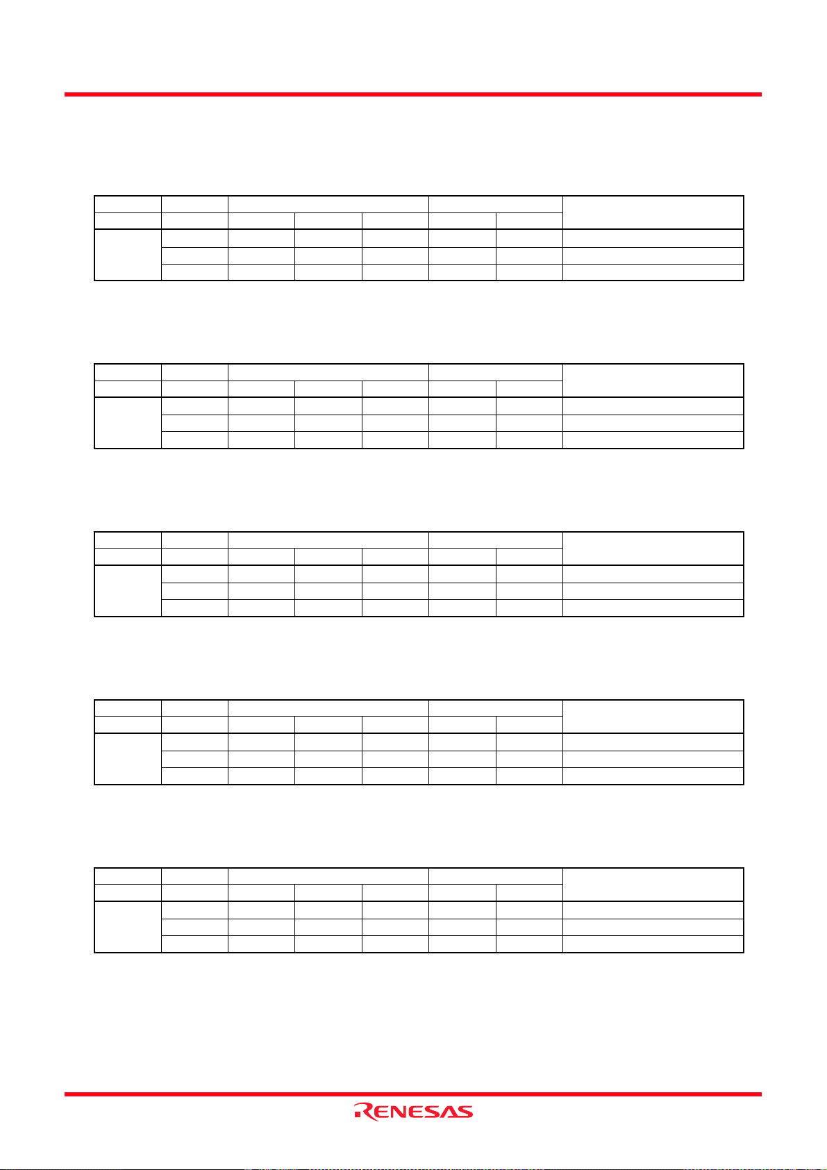
R8C/2C Group, R8C/2D Group 7. Programmable I/O Ports
7.4 Port settings
Tables 7.4 to 7.81 list the port settings.
Table 7.4 Port P0_0/AN7
Register PD0 ADCON0 ADCON2
Bit PD0_0 CH2 CH1 CH0 ADGSEL1 ADGSEL0
Setting
Value
X: 0 or 1
NOTE:
1. Pulled up by setting the PU00 bit in the PUR0 register to 1.
0XXXXX
1 X X X X X Output port
011100A/D converter input (AN7)
Table 7.5 Port P0_1/AN6
Register PD0 ADCON0 ADCON2
Bit PD0_1 CH2 CH1 CH0 ADGSEL1 ADGSEL0
Setting
Value
X: 0 or 1
NOTE:
1. Pulled up by setting the PU00 bit in the PUR0 register to 1.
0XXXXX
1 X X X X X Output port
011000A/D converter input (AN6)
Input port
Input port
Function
(1)
Function
(1)
Table 7.6 Port P0_2/AN5
Register PD0 ADCON0 ADCON2
Bit PD0_2 CH2 CH1 CH0 ADGSEL1 ADGSEL0
Setting
Value
X: 0 or 1
NOTE:
1. Pulled up by setting the PU00 bit in the PUR0 register to 1.
0XXXXX
1 X X X X X Output port
010100A/D converter input (AN5)
Table 7.7 Port P0_3/AN4
Register PD0 ADCON0 ADCON2
Bit PD0_3 CH2 CH1 CH0 ADGSEL1 ADGSEL0
Setting
Value
X: 0 or 1
NOTE:
1. Pulled up by setting the PU00 bit in the PUR0 register to 1.
0XXXXX
1 X X X X X Output port
010000A/D converter input (AN4)
Table 7.8 Port P0_4/AN3
Register PD0 ADCON0 ADCON2
Bit PD0_4 CH2 CH1 CH0 ADGSEL1 ADGSEL0
Setting
Value
X: 0 or 1
NOTE:
1. Pulled up by setting the PU01 bit in the PUR0 register to 1.
0XXXXX
1 X X X X X Output port
001100A/D converter input (AN3)
Input port
Input port
Input port
Function
(1)
Function
(1)
Function
(1)
Rev.2.00 Dec 05, 2007 Page 71 of 585
REJ09B0339-0200
Page 93

R8C/2C Group, R8C/2D Group 7. Programmable I/O Ports
Table 7.9 Port P0_5/AN2/CLK1
Register
Bit
Setting
Value
X: 0 or 1
NOTE:
1. Pulled up by setting the PU01 bit in the PUR0 register to 1.
PD0 ADCON0 ADCON2 PMR U1MR U1SR
PD0_5 CH2 CH1 CH0 ADGSEL1 ADGSEL0 U1PINSEL SMD2 SMD1 SMD0 CKDIR CLK11PSEL CLK10PSEL
X Other than 001b X X X
0 XXX X X
1 XXX X X
0010 0 0 X XXX X X X
0 XXX X X 1 X X X 1
X XXX X X 1 0 0 1 0
0 XXX X X X
X XXX 1 X X
X Other than 001b X X X
X XXX 0 X X
01
Function
(1)
Input port
Output port0 XXX X X X
A/D converter
input (AN2)
CLK1 (external
clock) input
CLK1 (internal
clock) output
Table 7.10 Port P0_6/AN1/DA0
Register PD0 ADCON0 ADCON2 DACON
Bit PD0_6 CH2 CH1 CH0 ADGSEL1 ADGSEL0 DA0E
0XXX X X X
Setting
Value
1 X X X X X X Output port
0 0 0 1 0 0 X A/D converter input (AN1)
0 X X X X X 1 D/A converter output (DA0)
X: 0 or 1
NOTE:
1. Pulled up by setting the PU01 bit in the PUR0 register to 1.
Input port
Function
(1)
Table 7.11 Port P0_7/AN0/DA1
Register PD0 ADCON0 ADCON2 DACON
Bit PD0_7 CH2 CH1 CH0 ADGSEL1 ADGSEL0 DA1E
0XXXXXX
Setting
Value
X: 0 or 1
NOTE:
1. Pulled up by setting the PU01 bit in the PUR0 register to 1.
1 X X X X X X Output port
0 0 0 0 0 0 X A/D converter input (AN0)
0 X X X X X 1 D/A converter output (DA1)
Input port
Function
(1)
Rev.2.00 Dec 05, 2007 Page 72 of 585
REJ09B0339-0200
Page 94

R8C/2C Group, R8C/2D Group 7. Programmable I/O Ports
Table 7.12 Port P1_0/KI0/AN8
Register PD1 KIEN ADCON0 ADCON2
Bit PD1_0 KI0EN CH2 CH1 CH0 ADGSEL1 ADGSEL0
0XXXXX X
Setting
Value
X: 0 or 1
NOTE:
1. Pulled up by setting the PU02 bit in the PUR0 register to 1.
1 X X X X X X Output port
0 1XXXX X
0 X 1 0 0 0 1 A/D converter input (AN8)
Input port
0 input
KI
Function
(1)
Table 7.13 Port P1_1/KI1/AN9
Register PD1 KIEN ADCON0 ADCON2
Bit PD1_1 KI1EN CH2 CH1 CH0 ADGSEL1 ADGSEL0
0XXXX X X
Setting
Value
X: 0 or 1
NOTE:
1. Pulled up by setting the PU02 bit in the PUR0 register to 1.
1 X X X X X X Output port
01XXXX X
0 X 1 0 1 0 1 A/D converter input (AN9)
Input port
1 input
KI
Function
(1)
Table 7.14 Port P1_2/KI2/AN10
Register PD1 KIEN ADCON0 ADCON2
Bit PD1_2 KI2EN CH2 CH1 CH0 ADGSEL1 ADGSEL0
0XXXX X X
Setting
Value
X: 0 or 1
NOTE:
1. Pulled up by setting the PU02 bit in the PUR0 register to 1.
1 X X X X X X Output port
01XXXX X
0 X 1 1 0 0 1 A/D converter input (AN10)
Table 7.15 Port P1_3/KI3/AN11
Register PD1 KIEN ADCON0 ADCON2
Bit PD1_3 KI3EN CH2 CH1 CH0 ADGSEL1 ADGSEL0
0XXXX X X
Setting
Value
X: 0 or 1
NOTE:
1. Pulled up by setting the PU02 bit in the PUR0 register to 1.
1 X X X X X X Output port
01XXXX X
0 X 1 1 1 0 1 A/D converter input (AN11)
Table 7.16 Port P1_4/TXD0
Register PD1 U0MR
Bit PD1_4 SMD2 SMD1 SMD0
0000
1 0 0 0 Output port
Setting
Value
X: 0 or 1
NOTES:
1. Pulled up by setting the PU03 bit in the PUR0 register to 1.
2. N-channel open-drain output by setting the NCH bit in the U0C0 register to 1.
X
001
100
101
110
Input port
TXD0 output
(1)
(2)
Function
Input port
2 input
KI
Input port
input
KI3
Function
(1)
Function
(1)
Rev.2.00 Dec 05, 2007 Page 73 of 585
REJ09B0339-0200
Page 95

R8C/2C Group, R8C/2D Group 7. Programmable I/O Ports
Table 7.17 Port P1_5/RXD0/(TRAIO)/(INT1)
Register PD1 TRAIOC TRAMR INTEN PMR
Bit PD1_5 TIOSEL TOPCR TMOD2 TMOD1 TMOD0 INT1EN INT1SEL
0XXXX
0
Setting
Value
X: 0 or 1
NOTE:
1. Pulled up by setting the PU03 bit in the PUR0 register to 1.
1
0
0 1 X Other than 001b X X TRAIO input
0 1 X Other than 001b 1 0
X 1 0 0 0 1 X X TRAIO pulse output
X1XXX
X X Other than 001b
0XXXX
X X Other than 001b
X
0001
X
Other than 001b
XX
X X Output portX1XXX
XX
Input port
RXD0 input
TRAIO/INT1
Function
(1)
(1)
input
Table 7.18 Port P1_6/CLK0
Register PD1 U0MR
Bit PD1_6 SMD2 SMD1 SMD0 CKDIR
Setting
Value
X: 0 or 1
NOTE:
1. Pulled up by setting the PU03 bit in the PUR0 register to 1.
0
1 Other than 001b X Output port
0 X X X 1 CLK0 (external clock) input
X 0 0 1 0 CLK0 (internal clock) output
Other than 001b X
XXX1
Input port
(1)
Function
Table 7.19 Port P1_7/TRAIO/INT1
Register PD1 TRAIOC TRAMR INTEN PMR
Bit PD1_7 TIOSEL TOPCR TMOD2 TMOD1 TMOD0 INT1EN INT1SEL
1XXXX
0
Setting
Value
X: 0 or 1
NOTE:
1. Pulled up by setting the PU03 bit in the PUR0 register to 1.
1
0 0 X Other than 001b X X TRAIO input
0 0 X Other than 001b 1 0
X 0 0 0 0 1 X X TRAIO pulse output
X1XXX
X X Other than 001b
1XXXX
X X Other than 001b
XX
X X Output portX1XXX
Input port
TRAIO/INT1
(1)
Function
input
Rev.2.00 Dec 05, 2007 Page 74 of 585
REJ09B0339-0200
Page 96

R8C/2C Group, R8C/2D Group 7. Programmable I/O Ports
Table 7.20 Port P2_0/TRDIOA0/TRDCLK
Register PD2 TRDOER1 TRDFCR TRDIORA0
Bit PD2_0 EA0 CMD1 CMD0 STCLK PWM3 IOA2 IOA1 IOA0
0 1 XXXXXXX
1 1 XXXXXXX
Setting
Value
0 X 0 0 0 1 1 X X Timer mode (input capture function)
0 X XX1 1000External clock input (TRDCLK)
X00000XXX
X00001
001
01X
X: 0 or 1
NOTES:
1. Pulled up by setting the PU04 bit in the PUR0 register to 1.
2. Output drive capacity high by setting the P2DRR0 bit in the P2DRR register to 1.
Input port
Output port
PWM3 mode waveform output
Timer mode waveform output
(output compare function)
Function
(1)
(2)
(2)
(2)
Table 7.21 Port P2_1/TRDIOB0
Register PD2 TRDOER1 TRDFCR TRDPMR TRDIORA0
Bit PD2_1 EB0 CMD1 CMD0 PWM3 PWMB0 IOB2 IOB1 IOB0
01XXXXXXX
11XXXXXXX
0 X 0 0 1 0 1 X X Timer mode (input capture function)
10
11
X X X X X Complementary PWM mode waveform output
001
01X
Setting
Value
X0
X001XXXXX
X0000XXXX
X00011XXX
X00010
X: 0 or 1
NOTES:
1. Pulled up by setting the PU04 bit in the PUR0 register to 1.
2. Output drive capacity high by setting the P2DRR1 bit in the P2DRR register to 1.
Input port
Output port
Reset synchronous PWM mode waveform output
PWM3 mode waveform output
PWM mode waveform output
Timer mode waveform output (output compare
function)
(1)
(2)
Function
(2)
(2)
(2)
Table 7.22 Port P2_2/TRDIOC0
Register PD2 TRDOER1 TRDFCR TRDPMR TRDIORC0
Bit PD2_2 EC0 CMD1 CMD0 PWM3 PWMC0 IOC2 IOC1 IOC0
0 1 XXX X XXX
1 1 XXX X XXX
0 X 0 0 1 0 1 X X Timer mode (input capture function)
Setting
Value
X0
X001XXXXX
X 0 001 1 XXX
X 0 001 0
X: 0 or 1
NOTES:
1. Pulled up by setting the PU04 bit in the PUR0 register to 1.
2. Output drive capacity high by setting the P2DRR2 bit in the P2DRR register to 1.
10
11
XXXXX
001
01X
Function
Input port
Output port
Complementary PWM mode waveform
output
Reset synchronous PWM mode waveform
output
PWM mode waveform output
Timer mode waveform output (output
compare function)
(1)
(2)
(2)
(2)
(2)
(2)
Rev.2.00 Dec 05, 2007 Page 75 of 585
REJ09B0339-0200
Page 97

R8C/2C Group, R8C/2D Group 7. Programmable I/O Ports
Table 7.23 Port P2_3/TRDIOD0
Register PD2 TRDOER1 TRDFCR TRDPMR TRDIORC0
Bit PD2_3 ED0 CMD1 CMD0 PWM3 PWMD0 IOD2 IOD1 IOD0
0 1 XXX X XXX
1 1 XXX X XXX
0 X 0 0 1 0 1 X X Timer mode (input capture function)
10
11
XXXXX
Setting
Value
X0
X001XXXXX
X 0 001 1 XXX
X 0 001 0
001
01X
X: 0 or 1
NOTES:
1. Pulled up by setting the PU04 bit in the PUR0 register to 1.
2. Output drive capacity high by setting the P2DRR3 bit in the P2DRR register to 1.
Input port
Output port
Complementary PWM mode waveform
(2)
output
Reset synchronous PWM mode waveform
(2)
output
PWM mode waveform output
Timer mode waveform output (output
compare function)
Function
(1)
(2)
(2)
(2)
Table 7.24 Port P2_4/TRDIOA1
Register PD2 TRDOER1 TRDFCR TRDIORA1
Bit PD2_4 EA1 CMD1 CMD0 PWM3 IOA2 IOA1 IOA0
0 1 XXXXXX
1 1 XXXXXX
0 X 0 0 1 1 X X Timer mode (input capture function)
Setting
Value
X0
10
11
XXXX
X001XXXX
X 0 001
001
01X
X: 0 or 1
NOTES:
1. Pulled up by setting the PU05 bit in the PUR0 register to 1.
2. Output drive capacity high by setting the P2DRR4 bit in the P2DRR register to 1.
Input port
Output port
(1)
(2)
Complementary PWM mode waveform output
Reset synchronous PWM mode waveform output
Timer mode waveform output
(output compare function)
Function
(2)
(2)
(2)
Table 7.25 Port P2_5/TRDIOB1
Register PD2 TRDOER1 TRDFCR TRDPMR TRDIORA1
Bit PD2_5 EB1 CMD1 CMD0 PWM3 PWMB1 IOB2 IOB1 IOB0
0 1 XXX X XXX
1 1 XXX X XXX
0 X 0 0 1 0 1 X X Timer mode (input capture function)
Setting
Value
X0
X001XXXXX
X 0 001 1 XXX
X 0 001 0
X: 0 or 1
NOTES:
1. Pulled up by setting the PU05 bit in the PUR0 register to 1.
2. Output drive capacity high by setting the P2DRR5 bit in the P2DRR register to 1.
10
11
XXXXX
001
01X
Function
Input port
Output port
(1)
(2)
Complementary PWM mode waveform
(2)
output
Reset synchronous PWM mode waveform
(2)
output
PWM mode waveform output
(2)
Timer mode waveform output (output
compare function)
(2)
Rev.2.00 Dec 05, 2007 Page 76 of 585
REJ09B0339-0200
Page 98

R8C/2C Group, R8C/2D Group 7. Programmable I/O Ports
Table 7.26 Port P2_6/TRDIOC1
Register PD2 TRDOER1 TRDFCR TRDPMR TRDIORC1
Bit PD2_6 EC1 CMD1 CMD0 PWM3 PWMC1 IOC2 IOC1 IOC0
0 1 XXX X XXX
1 1 XXX X XXX
0 X 0 0 1 0 1 X X Timer mode (input capture function)
10
11
XXXXX
Setting
Value
X0
X001XXXXX
X 0 001 1 XXX
X 0 001 0
001
01X
X: 0 or 1
NOTES:
1. Pulled up by setting the PU05 bit in the PUR0 register to 1.
2. Output drive capacity high by setting the P2DRR6 bit in the P2DRR register to 1.
Input port
Output port
Complementary PWM mode waveform
(2)
output
Reset synchronous PWM mode waveform
(2)
output
PWM mode waveform output
Timer mode waveform output (output
compare function)
Function
(1)
(2)
(2)
(2)
Table 7.27 Port P2_7/TRDIOD1
Register PD2 TRDOER1 TRDFCR TRDPMR TRDIORC1
Bit PD2_7 ED1 CMD1 CMD0 PWM3 PWMD1 IOD2 IOD1 IOD0
0 1 XXX X XXX
1 1 XXX X XXX
0 X 0 0 1 0 1 X X Timer mode (input capture function)
10
11
XXXXX
Setting
Value
X0
X001XXXXX
X 0 001 1 XXX
X 0 001 0
001
01X
X: 0 or 1
NOTES:
1. Pulled up by setting the PU05 bit in the PUR0 register to 1.
2. Output drive capacity high by setting the P2DRR7 bit in the P2DRR register to 1.
Input port
Output port
Complementary PWM mode waveform
(2)
output
Reset synchronous PWM mode waveform
(2)
output
PWM mode waveform output
Timer mode waveform output
(output compare function)
Function
(1)
(2)
(2)
(2)
Rev.2.00 Dec 05, 2007 Page 77 of 585
REJ09B0339-0200
Page 99

R8C/2C Group, R8C/2D Group 7. Programmable I/O Ports
Table 7.28 Port P3_0/TRAO
Register PD3 TRAIOC
Bit PD3_0 TOENA
Setting
Value
X: 0 or 1
NOTE:
1. Pulled up by setting the PU06 bit in the PUR0 register to 1.
00
1 0 Output port
X 1 TRAO output
Input port
(1)
Function
Table 7.29 Port P3_1/TRBO
Register PD3 TRBMR TRBIOC
Bit PD3_1 TMOD1 TMOD0 TOCNT
000X
Setting
Value
X: 0 or 1
NOTE:
1. Pulled up by setting the PU06 bit in the PUR0 register to 1.
100X
X 01b 1
X Other than 00b 0 TRBO output
Input port
Output port
(1)
Function
Table 7.30 Port P3_2/(INT2)
Register PD3 INTEN PMR
Bit PD3_2 INT2EN INT2SEL
Setting
Value
X: 0 or 1
NOTE:
1. Pulled up by setting the PU06 bit in the PUR0 register to 1.
0XX
1 X X Output port
011
Input port
input
INT2
(1)
Function
Table 7.31 Port P3_3/SSI
Clock Synchronous Serial I/O with Chip Select
Register PD3
Bit PD3_3 SSI output control SSI input control IICSEL
0
Setting
Value
X: 0 or 1
NOTES:
1. Pulled up by setting the PU06 bit in the PUR0 register to 1.
2. N-channel open-drain output by setting the SOOS bit in the SSMR2 register to 1 when this pin functions as output.
1
X 0 1 0 SSI input
X1 00
(Refer to Table 16.4 Association between
Communication Modes and I/O Pins
000
XX1
000
XX1
.)
PMR
Input port
Output port
SSI output
Function
(1)
(2)
(2)
Rev.2.00 Dec 05, 2007 Page 78 of 585
REJ09B0339-0200
Page 100

R8C/2C Group, R8C/2D Group 7. Programmable I/O Ports
Table 7.32 Port P3_4/SDA/SCS
Register PD3 SSMR2 PMR ICCR1
Bit PD3_4 CSS1 CSS0 IICSEL ICE
Setting
Value
0000X
000X0
1000X
100X0
X010X
X
10
11
0X
Input port
Output port
SCS
SCS output
(1)
(2)
input
(2)
X X X 1 1 SDA input/output
X: 0 or 1
NOTES:
1. Pulled up by setting the PU07 bit in the PUR0 register to 1.
2. N-channel open-drain output by setting the CSOS bit in the SSMR2 register to 1 when this pin functions as output.
Function
Table 7.33 Port P3_5/SCL/SSCK
Clock Synchronous Serial I/O with Chip Select
Register PD3
Bit PD3_5 SSCK output control SSCK input control IICSEL ICE
Setting
Value
X: 0 or 1
NOTES:
1. Pulled up by setting the PU07 bit in the PUR0 register to 1.
2. N-channel open-drain output by setting the SCKOS bit in the SSMR2 register to 1 when this pin functions as output.
(Refer to Table 16.4 Association between
Communication Modes and I/O Pins
00 00X
00 0X0
10 00X
10 0X0
.)
PMR ICCR1
Input port
Output port
(1)
(2)
X 0 1 0 0 SSCK input
X1 000
SSCK output
(2)
X 1 0 1 1 SCL input/output
Function
Table 7.34 Port P3_6/(INT1)
Register PD3 INTEN PMR
Bit PD3_6 INT1EN INT1SEL
Setting
Value
0XX
1 X X Output port
011
Input port
input
INT1
X: 0 or 1
NOTE:
1. Pulled up by setting the PU07 bit in the PUR0 register to 1.
Table 7.35 Port P3_7/SSO
Register PD3
Bit PD3_7 SSO output control SSO input control SOOS IICSEL
Setting
Value
X: 0 or 1
NOTE:
1. Pulled up by setting the PU07 bit in the PUR0 register to 1.
Clock Synchronous Serial I/O with Chip Select
(Refer to Table 16.4 Association between
Communication Modes and I/O Pins
0
1
00X0
XX 1
0000
XX 1
SSMR2 PMR
.)
X 0 1 0 0 SSO input
X 1 0 0 0 SSO output (CMOS output)
X1 0 10
Function
(1)
Function
Input port
(1)
Output port
SSO output (N-channel open-drain
output)
Rev.2.00 Dec 05, 2007 Page 79 of 585
REJ09B0339-0200
 Loading...