

Page 1

REJ09B0252-0110
16
R8C/1A Group, R8C/1B Group
Hardware Manual
RENESAS 16-BIT SINGLE-CHIP MICROCOMPUTER
M16C FAMILY / R8C/Tiny SERIES
All information contained in these materials, including products and product specifications,
represents information on the product at the time of publication and is subject to change by
Renesas Technology Corp. without notice. Please review the latest information published
by Renesas Technology Corp. through various means, including the Renesas Technology
Corp. website (http://www.renesas.com).
Rev.1.10
Revision Date: Mar 17, 2006
www.renesas.com
Page 2

Keep safety first in your circuit designs!
1.
Renesas Technology Corp. puts the maximum effort into making semiconductor products
better and more reliable, but there is always the possibility that trouble may occur with
them. Trouble with semiconductors may lead to personal injury, fire or property damage.
Remember to give due consideration to safety when making your circuit designs, with appropriate measures such as (i) placement of substitutive, auxiliary circuits, (ii) use of nonflammable material or (iii) prevention against any malfunction or mishap.
Notes regarding these materials
1.
These materials are intended as a reference to assist our customers in the selection of the
Renesas Technology Corp. product best suited to the customer's application; they do not
convey any license under any intellectual property rights, or any other rights, belonging to
Renesas Technology Corp. or a third party.
2.
Renesas Technology Corp. assumes no responsibility for any damage, or infringement of
any third-party's rights, originating in the use of any product data, diagrams, charts, programs, algorithms, or circuit application examples contained in these materials.
3.
All information contained in these materials, including product data, diagrams, charts, programs and algorithms represents information on products at the time of publication of these
materials, and are subject to change by Renesas Technology Corp. without notice due to
product improvements or other reasons. It is therefore recommended that customers contact Renesas Technology Corp. or an authorized Renesas Technology Corp. product distributor for the latest product information before purchasing a product listed herein.
The information described here may contain technical inaccuracies or typographical errors.
Renesas Technology Corp. assumes no responsibility for any damage, liability, or other
loss rising from these inaccuracies or errors.
Please also pay attention to information published by Renesas Technology Corp. by various means, including the Renesas Technology Corp. Semiconductor home page (http://
www.renesas.com).
4.
When using any or all of the information contained in these materials, including product
data, diagrams, charts, programs, and algorithms, please be sure to evaluate all information as a total system before making a final decision on the applicability of the information
and products. Renesas Technology Corp. assumes no responsibility for any damage, liability or other loss resulting from the information contained herein.
5.
Renesas Technology Corp. semiconductors are not designed or manufactured for use in a
device or system that is used under circumstances in which human life is potentially at
stake. Please contact Renesas Technology Corp. or an authorized Renesas Technology
Corp. product distributor when considering the use of a product contained herein for any
specific purposes, such as apparatus or systems for transportation, vehicular, medical,
aerospace, nuclear, or undersea repeater use.
6.
The prior written approval of Renesas Technology Corp. is necessary to reprint or reproduce in whole or in part these materials.
7.
If these products or technologies are subject to the Japanese export control restrictions,
they must be exported under a license from the Japanese government and cannot be imported into a country other than the approved destination.
Any diversion or reexport contrary to the export control laws and regulations of Japan and/
or the country of destination is prohibited.
8.
Please contact Renesas Technology Corp. for further details on these materials or the
products contained therein.
Page 3

General Precautions in the Handling of MPU/MCU Products
The following usage notes are applicable to all MPU/MC U pr o duct s fr om R e nesas. For d et a il ed usa ge not es on the
products covered by this manual, refer to the relevant sections of the manual. If the descriptions un der General
Precautions in the Handling of MPU/MCU Products and in the body of the manual differ from each other, the description
in the body of the manual takes precedence.
1. Handling of Unused Pins
Handle unused pins in accord with the directions given under Handling of Unused Pins in the manual.
The input pins of CMOS products are generally in the high-impedance state. In operation with an
unused pin in the open-circuit state, extra electromagnetic noise is induced in the vicinity of LSI, an
associated shoot-through current flows internally, and malfunctions occur due to the false
recognition of the pin state as an input signal become possible. Unused pins should be handled as
described under Handling of Unused Pins in the manual.
2. Processing at Power-on
The state of the product is undefined at the moment when power is supplied.
The states of internal circuits in the LSI are indeterminate and the states of register settings and pins
are undefined at the moment when power is supplied.
In a finished product where the reset signal is applied to the external reset pin, the states of pins are
not guaranteed from the moment when power is supplied until the reset process is completed.
In a similar way, the states of pins in a product that is reset by an on-chip power-on reset function
are not guaranteed from the moment when power is supplied until the power reaches the level at
which resetting has been specified.
3. Prohibition of Access to Reserved Addresses
Access to reserved addresses is prohibited.
The reserved addresses are provided for the possible future expansion of functions. Do not access
these addresses; the correct operation of LSI is not guaranteed if they are accessed.
4. Clock Signals
After applying a reset, only release the reset line after the operating clock signal has become stable.
When switching the clock signal during program execution, wait until the target clock signal has
stabilized.
When the clock signal is generated with an external resonator (or from an external oscillator) during
a reset, ensure that the reset line is only released after full stabilization of the clock signal. Moreover,
when switching to a clock signal produced with an external resonator (or by an external oscillator)
while program execution is in progress, wait until the target clock signal is stable.
5. Differences between Products
Before changing from one product to another, i.e. to one with a different type number, confirm that the
change will not lead to problems.
The characteristics of MPU/MCU in the same group but having different type numbers may differ
because of the differences in internal memory capacity and layout pattern. When changing to
products of different type numbers, implement a system-evaluation test for each of the products.
Page 4

How to Use This Manual
1. Purpose and Target Readers
This manual is designed to provide the user with an understanding of the hardware functions and electrical
characteristics of the MCU. It is intended for users designing application systems incorporating the MCU. A basic
knowledge of electric circuits, logical circuits, and MCUs is necessary in order to use this manual.
The manual comprises an overview of the product; descriptions of the CPU, system control functions, peripheral
functions, and electrical characteristics; and usage notes.
Particular attention should be paid to the precautionary notes when using the manual. These notes occur
within the body of the text, at the end of each section, and in the Usage Notes section.
The revision history summarizes the locations of revisions and additions. It does not list all revisions. Refer
to the text of the manual for details.
The following documents apply to the R8C/1A Group, R8C/1B Group. Make sure to refer to the latest versions of
these documents. The newest versions of the documents li sted may be obtained fro m the Renesas Technology Web
site.
Document Type Description Document Title Document No.
Datasheet Hardware overview and electrical characteristics R8C/1A Group,
R8C/1B Group
Datasheet
Hardware manual Hardware specifications (pin assignments,
memory maps, peripheral function
specifications, electrical characteristics, timing
charts) and operation description
Note: Refer to the application notes for details on
using peripheral functions.
Software manual Description of CPU instruction set R8C/Tiny Series
Application note Information on using peripheral functions and
application examples
Sample programs
Information on writing programs in assembly
language and C
Renesas
technical update
Product specifications, updates on documents,
etc.
R8C/1A Group,
R8C/1B Group
Hardware Manual
Software Manual
Available from Renesas
Technology Web site.
REJ03B0144
This hardware
manual
REJ09B0001
Page 5

2. Notation of Numbers and Symbols
The notation conventions for register names, bit names, numbers, and symbols used in this manual are described
below.
(1) Register Names, Bit Names, and Pin Names
Registers, bits, and pins are referred to in the text by symbols. The symbol is accompanied by the word
“register,” “bit,” or “pin” to distinguish the three categories.
Examples the PM03 bit in the PM0 register
P3_5 pin, VCC pin
(2) Notation of Numbers
The indication “b” is appended to numeric valu es given i n binary format. However, nothing is appended to the
values of single bits. The indication “h” is appended to numeric values given in hexadecimal format. Nothing
is appended to numeric values given in decimal format.
Examples Binary: 11b
Hexadecimal: EFA0h
Decimal: 1234
Page 6
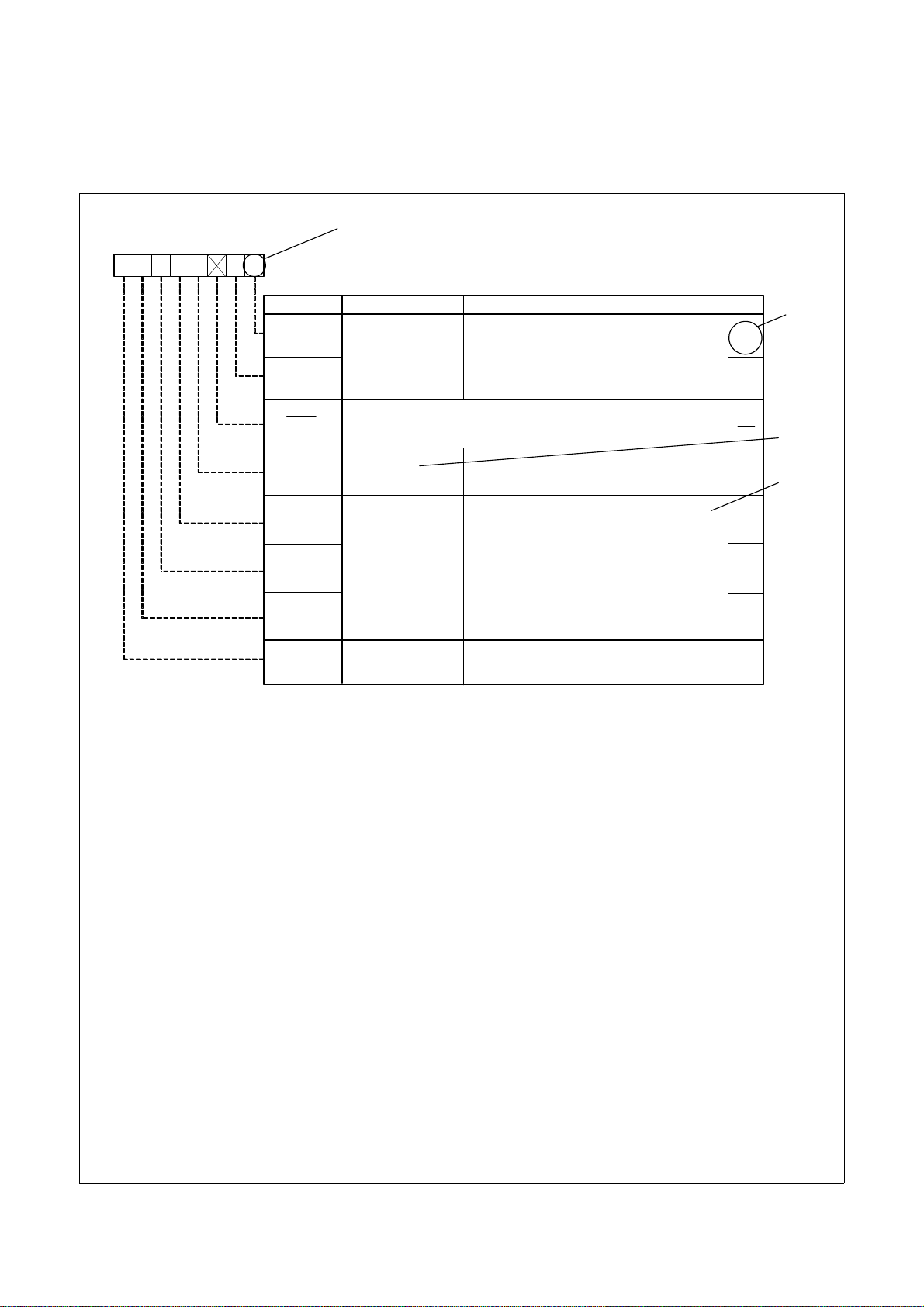
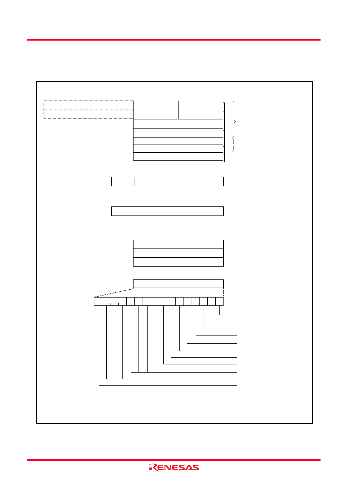
3. Register Notation
The symbols and terms used in register diagrams are described below.
XXX Register
b7 b6 b5 b4 b3 b2 b1 b0
0
XXX0
XXX1
(b2)
(b3)
XXX4
XXX5
XXX6
XXX7
*1
Symbol Address After Reset
XXX XXX 00h
Bit NameBit Symbol
XXX bits
Nothing is assigned. If necessary, set to 0.
When read, the content is undefined.
Reserved bits
XXX bits
XXX bit
b1 b0
1 0: XXX
0 1: XXX
1 0: Do not set.
1 1: XXX
Set to 0.
Function varies according to the operating
mode.
0: XXX
1: XXX
Function
RW
RW
RW
RW
RW
WO
RW
RO
*2
*3
*4
*1
Blank: Set to 0 or 1 according to the application.
0: Set to 0.
1: Set to 1.
X: Nothing is assigned.
*2
RW: Read and write.
RO: Read only.
WO: Write only.
−: Nothing is assigned.
*3
• Reserved bit
Reserved bit. Set to specified value.
*4
• Nothing is assigned
Nothing is assigned to the bit. As the bit may be used for future functions, if necessary, set to 0.
• Do not set to a value
Operation is not guaranteed when a value is set.
• Function varies according to the operating mode.
The function of the bit varies with the peripheral function mode. Refer to the register diagram for information
on the individual modes.
Page 7

4. List of Abbreviations and Acronyms
Abbreviation Full Form
ACIA Asynchronous Communication Interface Adapter
bps bits per second
CRC Cyclic Redundancy Check
DMA Direct Memory Access
DMAC Direct Memory Access Controller
GSM Global System for Mobile Communications
Hi-Z High Impedance
IEBus Inter Equipment bus
I/O Input/Output
IrDA Infrared Data Association
LSB Least Significant Bit
MSB Most Significant Bit
NC Non-Connection
PLL Phase Locked Loop
PWM Pulse Width Modulation
SFR Special Function Registers
SIM Subscriber Identity Module
UART Universal Asynchronous Receiver/Transmitter
VCO Voltage Controlled Oscillator
Page 8

Table of Contents
SFR Page Reference B - 1
1. Overview 1
1.1 Applications.................................................................................................1
1.2 Performance Overview................................................................................2
1.3 Block Diagram.............................................................................................4
1.4 Product Information.....................................................................................5
1.5 Pin Assignments..........................................................................................7
1.6 Pin Functions.............................................................................................10
2. Central Processing Unit (CPU) 13
2.1 Data Registers (R0, R1, R2, and R3)........................................................14
2.2 Address Registers (A0 and A1).................................................................14
2.3 Frame Base Register (FB) ........................................................................14
2.4 Interrupt Table Register (INTB).................................................................14
2.5 Program Counter (PC) ..............................................................................14
2.6 User Stack Pointer (USP) and Interrupt Stack Pointer (ISP).....................14
2.7 Static Base Register (SB)..........................................................................14
2.8 Flag Register (FLG)...................................................................................14
2.8.1 Carry Flag (C).....................................................................................14
2.8.2 Debug Flag (D)...................................................................................14
2.8.3 Zero Flag (Z).......................................................................................14
2.8.4 Sign Flag (S).......................................................................................14
2.8.5 Register Bank Select Flag (B)............................................................14
2.8.6 Overflow Flag (O)...............................................................................14
2.8.7 Interrupt Enable Flag (I)......................................................................15
2.8.8 Stack Pointer Select Flag (U).............................................................15
2.8.9 Processor Interrupt Priority Level (IPL) ..............................................15
2.8.10 Reserved Bit.......................................................................................15
3. Memory 16
3.1 R8C/1A Group...........................................................................................16
3.2 R8C/1B Group...........................................................................................17
A - 1
Page 9

4. Special Function Registers (SFRs) 18
5. Programmable I/O Ports 22
5.1 Functions of Programmable I/O Ports.......................................................22
5.2 Effect on Peripheral Functions..................................................................22
5.3 Pins Other than Programmable I/O Ports..................................................22
5.4 Port Settings..............................................................................................30
5.5 Unassigned Pin Handling..........................................................................35
6. Resets 36
6.1 Hardware Reset ........................................................................................38
6.1.1 When Power Supply is Stable............................................................38
6.1.2 Power On............................................................................................38
6.2 Power-On Reset Function.........................................................................40
6.3 Voltage Monitor 1 Reset ...........................................................................41
6.4 Voltage Monitor 2 Reset............................................................................41
6.5 Watchdog Timer Reset..............................................................................41
6.6 Software Reset..........................................................................................41
7. Voltage Detection Circuit 42
7.1 VCC Input Voltage.....................................................................................48
7.1.1 Monitoring Vdet1 ................................................................................48
7.1.2 Monitoring Vdet2 ................................................................................48
7.1.3 Digital Filter.........................................................................................48
7.2 Voltage Monitor 1 Reset............................................................................50
7.3 Voltage Monitor 2 Interrupt and Voltage Monitor 2 Reset......................... 51
8. Processor Mode 53
8.1 Processor Modes ...................................................................................... 53
9. Bus 55
10. Clock Generation Circuit 56
10.1 Main Clock.................................................................................................63
10.2 On-Chip Oscillator Clocks.........................................................................64
10.2.1 Low-Speed On-Chip Oscillator Clock.................................................64
10.2.2 High-Speed On-Chip Oscillator Clock................................................64
A - 2
Page 10

10.3 CPU Clock and Peripheral Function Clock................................................65
10.3.1 System Clock......................................................................................65
10.3.2 CPU Clock..........................................................................................65
10.3.3 Peripheral Function Clock (f1, f2, f4, f8, f32)......................................65
10.3.4 fRING and fRING128..........................................................................65
10.3.5 fRING-fast...........................................................................................65
10.3.6 fRING-S..............................................................................................65
10.4 Power Control............................................................................................66
10.4.1 Standard Operating Mode..................................................................66
10.4.2 Wait Mode ..........................................................................................67
10.4.3 Stop Mode..........................................................................................69
10.5 Oscillation Stop Detection Function..........................................................71
10.5.1 How to Use Oscillation Stop Detection Function................................71
10.6 Notes on Clock Generation Circuit............................................................73
10.6.1 Stop Mode and Wait Mode.................................................................73
10.6.2 Oscillation Stop Detection Function....................................................73
10.6.3 Oscillation Circuit Constants...............................................................73
10.6.4 High-Speed On-Chip Oscillator Clock................................................73
11. Protection 74
12. Interrupts 75
12.1 Interrupt Overview.....................................................................................75
12.1.1 Types of Interrupts..............................................................................75
12.1.2 Software Interrupts.............................................................................76
12.1.3 Special Interrupts................................................................................77
12.1.4 Peripheral Function Interrupt..............................................................77
12.1.5 Interrupts and Interrupt Vectors..........................................................78
12.1.6 Interrupt Control..................................................................................80
12.2 INT Interrupt..............................................................................................88
12.2.1 INT0 Interrupt .....................................................................................88
12.2.2 INT0 Input Filter..................................................................................89
12.2.3 INT1 Interrupt .....................................................................................90
12.2.4 INT3 Interrupt .....................................................................................91
12.3 Key Input Interrupt.....................................................................................93
12.4 Address Match Interrupt............................................................................95
A - 3
Page 11

12.5 Notes on Interrupts....................................................................................97
12.5.1 Reading Address 00000h...................................................................97
12.5.2 SP Setting...........................................................................................97
12.5.3 External Interrupt and Key Input Interrupt ..........................................97
12.5.4 Watchdog Timer Interrupt...................................................................97
12.5.5 Changing Interrupt Sources................................................................98
12.5.6 Changing Interrupt Control Register Contents ...................................99
13. Watchdog Timer 100
13.1 Count Source Protection Mode Disabled................................................103
13.2 Count Source Protection Mode Enabled.................................................104
14. Timers 105
14.1 Timer X....................................................................................................106
14.1.1 Timer Mode ......................................................................................109
14.1.2 Pulse Output Mode...........................................................................110
14.1.3 Event Counter Mode.........................................................................112
14.1.4 Pulse Width Measurement Mode .....................................................113
14.1.5 Pulse Period Measurement Mode....................................................116
14.1.6 Notes on Timer X..............................................................................119
14.2 Timer Z....................................................................................................120
14.2.1 Timer Mode ......................................................................................125
14.2.2 Programmable Waveform Generation Mode....................................127
14.2.3 Programmable One-shot Generation Mode .....................................130
14.2.4 Programmable Wait One-Shot Generation Mode.............................133
14.2.5 Notes on Timer Z..............................................................................137
14.3 Timer C....................................................................................................138
14.3.1 Input Capture Mode..........................................................................144
14.3.2 Output Compare Mode.....................................................................146
14.3.3 Notes on Timer C .............................................................................148
15. Serial Interface 149
15.1 Clock Synchronous Serial I/O Mode .......................................................155
15.1.1 Polarity Select Function....................................................................158
15.1.2 LSB First/MSB First Select Function................................................158
15.1.3 Continuous Receive Mode ...............................................................159
A - 4
Page 12

15.2 Clock Asynchronous Serial I/O (UART) Mode ........................................160
15.2.1 CNTR0 Pin Select Function..............................................................163
15.2.2 Bit Rate.............................................................................................164
15.3 Notes on Serial Interface......................................................................... 165
16. Clock Synchronous Serial Interface 166
16.1 Mode Selection........................................................................................166
16.2 Clock Synchronous Serial I/O with Chip Select (SSU)............................167
16.2.1 Transfer Clock..................................................................................176
16.2.2 SS Shift Register (SSTRSR)............................................................178
16.2.3 Interrupt Requests............................................................................179
16.2.4 Communication Modes and Pin Functions.......................................180
16.2.5 Clock Synchronous Communication Mode.......................................181
16.2.6 Operation in 4-Wire Bus Communication Mode...............................188
16.2.7 SCS Pin Control and Arbitration.......................................................194
16.2.8 Notes on Clock Synchronous Serial I/O with Chip Select ................195
16.3 I2C bus Interface .....................................................................................196
16.3.1 Transfer Clock..................................................................................206
16.3.2 Interrupt Requests............................................................................207
16.3.3 I2C bus Interface Mode.....................................................................208
16.3.4 Clock Synchronous Serial Mode ......................................................219
16.3.5 Noise Canceller................................................................................222
16.3.6 Bit Synchronization Circuit................................................................223
16.3.7 Examples of Register Setting...........................................................224
16.3.8 Notes on I2C bus Interface...............................................................228
17. A/D Converter 229
17.1 One-Shot Mode.......................................................................................233
17.2 Repeat Mode........................................................................................... 235
17.3 Sample and Hold.....................................................................................237
17.4 A/D Conversion Cycles ...........................................................................237
17.5 Internal Equivalent Circuit of Analog Input Block ....................................238
17.6 Inflow Current Bypass Circuit..................................................................239
17.7 Output Impedance of Sensor under A/D Conversion..............................240
17.8 Notes on A/D Converter..........................................................................242
A - 5
Page 13

18. Flash Memory 243
18.1 Overview.................................................................................................243
18.2 Memory Map...........................................................................................245
18.3 Functions to Prevent Rewriting of Flash Memory....................................247
18.3.1 ID Code Check Function ..................................................................247
18.3.2 ROM Code Protect Function ............................................................248
18.4 CPU Rewrite Mode..................................................................................249
18.4.1 EW0 Mode........................................................................................250
18.4.2 EW1 Mode........................................................................................250
18.4.3 Software Commands........................................................................259
18.4.4 Status Register.................................................................................263
18.4.5 Full Status Check .............................................................................264
18.5 Standard Serial I/O Mode........................................................................ 266
18.5.1 ID Code Check Function ..................................................................266
18.6 Parallel I/O Mode.....................................................................................270
18.6.1 ROM Code Protect Function ............................................................270
18.7 Notes on Flash Memory..........................................................................271
18.7.1 CPU Rewrite Mode...........................................................................271
19. Electrical Characteristics 273
20. Usage Notes 293
20.1 Notes on Clock Generation Circuit..........................................................293
20.1.1 Stop Mode and Wait Mode...............................................................293
20.1.2 Oscillation Stop Detection Function..................................................293
20.1.3 Oscillation Circuit Constants.............................................................293
20.1.4 High-Speed On-Chip Oscillator Clock..............................................293
20.2 Notes on Interrupts..................................................................................294
20.2.1 Reading Address 00000h.................................................................294
20.2.2 SP Setting.........................................................................................294
20.2.3 External Interrupt and Key Input Interrupt ........................................294
20.2.4 Watchdog Timer Interrupt.................................................................294
20.2.5 Changing Interrupt Sources..............................................................295
20.2.6 Changing Interrupt Control Register Contents .................................296
20.3 Precautions on Timers............................................................................297
20.3.1 Notes on Timer X..............................................................................297
A - 6
Page 14

20.3.2 Notes on Timer Z..............................................................................297
20.3.3 Notes on Timer C .............................................................................298
20.4 Notes on Serial Interface.........................................................................299
20.5 Precautions on Clock Synchronous Serial Interface...............................300
20.5.1 Notes on Clock Synchronous Serial I/O with Chip Select ................300
20.5.2 Notes on I2C bus Interface...............................................................301
20.6 Notes on A/D Converter..........................................................................302
20.7 Notes on Flash Memory..........................................................................303
20.7.1 CPU Rewrite Mode...........................................................................303
20.8 Notes on Noise........................................................................................305
20.8.1 Inserting a Bypass Capacitor between VCC and VSS Pins as a
Countermeasure against Noise and Latch-Up .................................305
20.8.2 Countermeasures against Noise Error of Port Control Registers.....305
21. Notes on On-Chip Debugger 306
Appendix 1. Package Dimensions 307
Appendix 2. Connection Examples between Serial Writer and On-Chip
Debugging Emulator 309
Appendix 3. Example of Oscillation Evaluation Circuit 310
Register Index 311
A - 7
Page 15

SFR Page Reference
Address Register Symbol Page
0000h
0001h
0002h
0003h
0004h Processor Mode Register 0 PM0 53
0005h Processor Mode Register 1 PM1 54
0006h System Clock Control Register 0 CM0 58
0007h System Clock Control Register 1 CM1 59
0008h
0009h Address Match Interrupt Enable Register AIER 96
000Ah Protect Register PRCR 74
000Bh
000Ch Oscillation Stop Detection Register OCD 60
000Dh Watchdog Timer Reset Register WDTR 102
000Eh Watchdog Timer Start Register WDTS 102
000Fh Watchdog Timer Control Register WDC 101
0010h Address Match Interrupt Register 0 RMAD0 96
0011h
0012h
0013h
0014h Address Match Interrupt Register 1 RMAD1 96
0015h
0016h
0017h
0018h
0019h
001Ah
001Bh
001Ch Count Source Protection Mode Register CSPR 102
001Dh
001Eh
INT0 Input Filter Select Register
001Fh
0020h High-Speed On-Chip Oscillator Control
Register 0
0021h High-Speed On-Chip Oscillator Control
Register 1
0022h High-Speed On-Chip Oscillator Control
Register 2
0023h
0024h
0025h
0026h
0027h
0028h
0029h
002Ah
002Bh
002Ch
002Dh
002Eh
002Fh
0030h
0031h Voltage Detection Register 1 VCA1 45
0032h Voltage Detection Register 2 VCA2 45
0033h
0034h
0035h
0036h Voltage Monitor 1 Circuit Control Register VW1C 46
0037h Voltage Monitor 2 Circuit Control Register VW2C 47
0038h
0039h
003Ah
003Bh
003Ch
003Dh
003Eh
003Fh
INT0F 88
HRA0 61
HRA1 62
HRA2 62
NOTE:
1. The blank regions are reserved.
Do not access locations in these regions.
Address Register Symbol Page
0040h
0041h
0042h
0043h
0044h
0045h
0046h
0047h
0048h
0049h
004Ah
004Bh
004Ch
004Dh Key Input Interrupt Control Register KUPIC 80
004Eh A/D Conversion Interru pt Con trol Register ADIC 80
004Fh SSU/IIC Interrupt Control Register SSUAIC/IIC2AIC 80
0050h Compare 1 Interrupt Control Register CMP1IC 80
0051h UART0 Transmit Interrupt Control Register S0TIC 80
0052h UART0 Receive Interrupt Control Register S0RIC 80
0053h UART1 Transmit Interrupt Control Register S1TIC 80
0054h UART1 Receive Interrupt Control Register S1RIC 80
0055h
0056h Timer X Interrupt Control Register TXIC 80
0057h
0058h Timer Z Interrupt Control Registe r TZIC 80
0059h INT1 Interrupt Control Register INT1IC 80
005Ah INT3 Interrupt Control Register INT3IC 80
005Bh Timer C Interrupt Control Register TCIC 80
005Ch Compare 0 Interrupt Control Register CMP0IC 80
005Dh INT0 Interrupt Control Register INT0IC 81
005Eh
005Fh
0060h
0061h
0062h
0063h
0064h
0065h
0066h
0067h
0068h
0069h
006Ah
006Bh
006Ch
006Dh
006Eh
006Fh
0070h
0071h
0072h
0073h
0074h
0075h
0076h
0077h
0078h
0079h
007Ah
007Bh
007Ch
007Dh
007Eh
007Fh
B - 1
Page 16
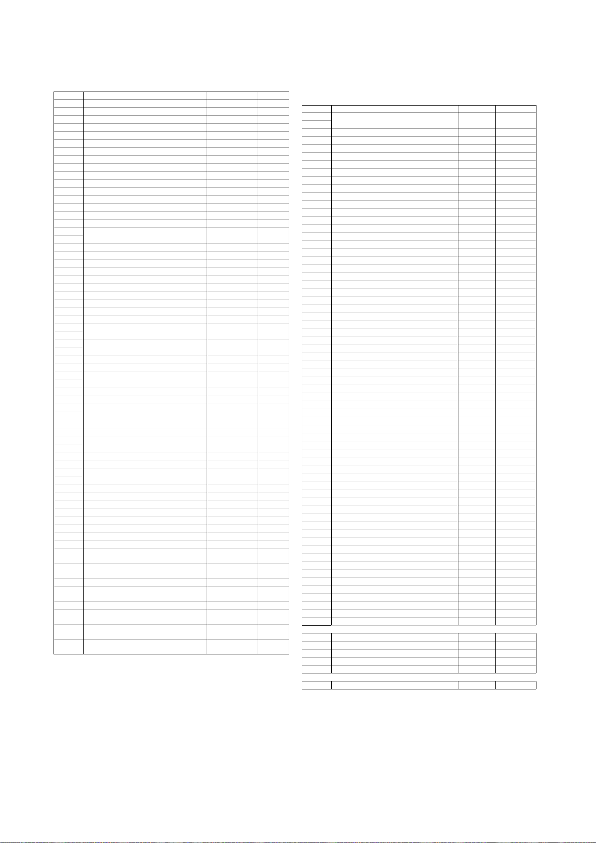
Address Register Symbol Page
0080h Timer Z Mode Register TZMR 121
0081h
0082h
0083h
0084h Timer Z Waveform Output Control Register PUM 123
0085h Prescaler Z Register PREZ 122
0086h Timer Z Secondary Register TZSC 122
0087h Timer Z Primary Register TZPR 122
0088h
0089h
008Ah Timer Z Output Control Register TZOC 123
008Bh Timer X Mode Register TXMR 107
008Ch Prescaler X Register PREX 108
008Dh Timer X Register TX 108
008Eh Timer Count Source Setting Register TCSS 108,124
008Fh
0090h Timer C Register TC 140
0091h
0092h
0093h
0094h
0095h
0096h External Input Enable Register INTEN 88
0097h
0098h Key Input Enable Register KIEN 94
0099h
009Ah Timer C Control Register 0 TCC0 141
009Bh Timer C Control Register 1 TCC1 142
009Ch Capture, Compare 0 Register TM0 140
009Dh
009Eh Compare 1 Register TM1 140
009Fh
00A0h UART0 Transmit/Receive Mode Register U0MR 152
00A1h UART0 Bit Rate Register U0BRG 151
00A2h UART0 Transmit Buffer Register U0TB 151
00A3h
00A4h UART0 Transmit/Receive Control R eg ister 0 U0C0 153
00A5h UART0 Transmit/Receive Control R eg ister 1 U0C1 154
00A6h UART0 Receive Buffer Register U0RB 151
00A7h
00A8h UART1 Transmit/Receive Mode Register U1MR 152
00A9h UART1 Bit Rate Register U1BRG 151
00AAh UART1 Transmit Buffer Register U1TB 151
00ABh
00ACh UART1 Transmit/Receive Control Register 0 U1C0 153
00ADh UART1 Transmit/Receive Control Register 1 U1C1 154
00AEh UART1 Receive Buffer Register U1RB 151
00AFh
00B0h UART Transmit/Receive Control Register 2 UCON 154
00B1h
00B2h
00B3h
00B4h
00B5h
00B6h
00B7h
00B8h SS Control Register H / IIC bus Control
Register 1
00B9h SS Control Register L / IIC bus Control
Register 2
00BAh SS Mode Register / IIC bus Mode Register SSMR / ICMR 171, 201
00BBh SS Enable Register / IIC bus Interrupt
Enable Register
00BCh SS Status Register / IIC bus Status Register SSSR / ICSR 173, 203
00BDh SS Mode Register 2 / Slave Address
Register
00BEh SS Transmit Data Register / IIC bus
Transmit Data Register
00BFh SS Receive Data Register / IIC bus Receive
Data Register
SSCRH / ICCR1 169, 199
SSCRL / ICCR2 170, 200
SSER / ICIER 172, 202
SSMR2 / SAR 174, 204
SSTDR / ICDRT 175, 204
SSRDR / ICDRR 175, 205
NOTE:
1. The blank regions, 0100h to 01B2h, and 01C0h to 02FFh
are reserved.
Do not access locations in these regions.
Address Register Symbol Page
00C0h A/D Register AD 232
00C1h
00C2h
00C3h
00C4h
00C5h
00C6h
00C7h
00C8h
00C9h
00CAh
00CBh
00CCh
00CDh
00CEh
00CFh
00D0h
00D1h
00D2h
00D3h
00D4h A/D Control Register 2 ADCON2 232
00D5h
00D6h A/D Control Register 0 ADCON0 231
00D7h A/D Control Register 1 ADCON1 231
00D8h
00D9h
00DAh
00DBh
00DCh
00DDh
00DEh
00DFh
00E0h
00E1h Port P1 Register P1 27
00E2h
00E3h Port P1 Direction Register PD1 27
00E4h
00E5h Port P3 Register P3 27
00E6h
00E7h Port P3 Direction Register PD3 27
00E8h Port P4 Register P4 28
00E9h
00EAh Port P4 Direction Register PD4 27
00EBh
00ECh
00EDh
00EEh
00EFh
00F0h
00F1h
00F2h
00F3h
00F4h
00F5h
00F6h
00F7h
00F8h Port Mode Register PMR 28, 175, 205
00F9h
00FAh
00FBh
00FCh Pull-Up Control Register 0 PUR0 29
00FDh Pull-Up Control Register 1 PUR1 29
00FEh Port P1 Drive Capacity Control Register DRR 29
00FFh Timer C Output Control Register TCOUT 143
01B3h Flash Memory Control Register 4 FMR4 255
01B4h
01B5h Flash Memory Control Register 1 FMR1 254
01B6h
01B7h Flash Memory Control Register 0 FMR0 253
0FFFFh Optional Function Select Register OFS 101, 248
B - 2
Page 17

R8C/1A Group, R8C/1B Group
REJ09B0252-0110
SINGLE-CHIP 16-BIT CMOS MICROCOMPUTER
Mar 17, 2006
1. Overview
These MCUs are fabricated using the high-performance silicon gate CMOS process, embedding the R8C/
Tiny Series CPU core, and is p ackaged in a 20-pin molded- plastic LSSOP, SDIP or a 28-pin plastic moldedHWQFN. It implements sophisticated instructions for a high level of instruction efficiency. With 1 Mbyte of
address space, they are capable of executing instructions at high speed.
Furthermore, the R8C/1B Group has on-chip data flash ROM (1 KB × 2 blocks).
The difference between the R8C/1A Group and R8C/1B Group is only the presence or absence of data
flash ROM. Their peripheral functions are the same.
1.1 Applications
Electric household appliances, office equipment, housing equipment (sensors, security systems),
general industrial equipment, audio equipment, etc.
Rev.1.10
Rev.1.10 Mar 17, 2006 Page 1 of 312
REJ09B0252-0110
Page 18
R8C/1A Group, R8C/1B Group 1. Overview
1.2 Performance Overview
Table 1.1 outlines the Functions and Specifications for R8C/1A Group and Table 1.2 outlines the
Functions and Specifications for R8C/1B Group.
Table 1.1 Functions and Specifications for R8C/1A Group
Item Specification
CPU Number of fundamental
instructions
Minimum instruction execution
time
Operating mode Single-chip
Address space 1 Mbyte
Memory capacity See Table 1.3 Product Information for R8C/1A Group
Peripheral
Functions
Electric
Characteristics
Flash Memory Programming and erasure voltage VCC = 2.7 to 5.5 V
Operating Ambient Temperature -20 to 85°C
Package 20-pin molded-plastic LSSOP
NOTE:
1. I2C bus is a trademark of Koninklijke Philips Electronics N. V.
Ports I/O ports: 13 pins (including LED drive port)
LED drive ports I/O ports: 4 pins
Timers Timer X: 8 bits × 1 channel, timer Z: 8 bits × 1 channel
Serial interfaces 1 channel
Clock synchronous serial interface 1 channel
A/D converter 10-bit A/D converter: 1 circuit, 4 channels
Watchdog timer 15 bits × 1 channel (with prescaler)
Interrupts Internal: 9 sources, External: 4 sources, Sof tware: 4 sources,
Clock generation circuits 2 circuits
Oscillation stop detection function Main clock oscillation stop detection function
Voltage detection circuit On-chip
Power-on reset circuit On-chip
Supply voltage VCC = 3.0 to 5.5 V (f(XIN) = 20 MHz)
Current consumption Typ . 9 m A
Programming and erasure
endurance
89 instructions
50 ns (f(XIN) = 20 MHz, VCC = 3.0 to 5.5 V)
100 ns (f(XIN) = 10 MHz, VCC = 2.7 to 5.5 V)
Input port: 3 pins
(Each timer equipped with 8-bit prescaler)
Timer C: 16 bits × 1 channel
(Input capture and output compare circuits)
Clock synchronous serial I/O, UART
1 channel
UART
2
C bus Interface
I
Clock synchronous serial I/O with chip select (SSU)
Reset start selectable, count source protection mode
Priority levels: 7 levels
• Main clock oscillation circuit (with on-chip feedback
resistor)
• On-chip oscillator (high speed, low speed)
High-speed on-chip oscillator has frequency adjustment
function
VCC = 2.7 to 5.5 V (f(XIN) = 10 MHz)
(VCC = 5.0 V , f(XIN) = 20 M Hz, A/D converter stopped )
Typ. 5 mA
Typ. 35 µA (VCC = 3.0 V, wait mode, peripheral clock off)
Typ. 0.7 µA (VCC = 3.0 V, stop mode)
100 times
-40 to 85°C (D version)
20-pin molded-plastic SDIP
28-pin molded-plastic HWQFN
(VCC = 3.0 V, f(XIN) = 10 MHz, A/D converter stopped)
(1)
Rev.1.10 Mar 17, 2006 Page 2 of 312
REJ09B0252-0110
Page 19
R8C/1A Group, R8C/1B Group 1. Overview
Table 1.2 Functions and Specifications for R8C/1B Group
Item Specification
CPU Number of fundamental
instructions
Minimum instruction execution
time
Operating mode Single-chip
Address space 1 Mbyte
Memory capacity See Table 1.4 Product Information for R8C/1B Group
Peripheral
Functions
Electric
Characteristics
Flash Memory Programming and erasure voltage VCC = 2.7 to 5.5 V
Operating Ambient Temperature -20 to 85°C
Package 20-pin molded-plastic LSSOP
NOTE:
1. I2C bus is a trademark of Koninklijke Philips Electronics N. V.
Ports I/O ports: 13 pins (including LED drive port)
LED drive ports I/O port s: 4 pins
Timers Timer X: 8 bits × 1 channel, timer Z: 8 bits × 1 channel
Serial interfaces 1 channel
Clock synchronous serial interface 1 channel
A/D converter 10-bit A/D converter: 1 circuit, 4 channels
Watchdog timer 15 bits × 1 channel (with prescaler)
Interrupts Internal: 9 sources, External: 4 sources, Software: 4 sources,
Clock generation circuits 2 circuits
Oscillation stop detection function Main clock oscillation stop detection function
Voltage detection circuit On-chip
Power on reset circuit On-chip
Supply voltage VCC = 3.0 to 5.5 V (f(XIN) = 20 MHz)
Current consumption T yp. 9 mA
Programming and erasure
endurance
89 instructions
50 ns (f(XIN) = 20 MHz, VCC = 3.0 to 5.5 V)
100 ns (f(XIN) = 10 MHz, VCC = 2.7 to 5.5 V)
Input port: 3 pins
(Each timer equipped with 8-bit prescaler)
Timer C: 16 bits × 1 channel
(Input capture and output compare circuits)
Clock synchronous serial I/O, UART
1 channel
UART
2
C bus Interface
I
Clock synchronous serial I/O with chip select (SSU)
Reset start selectable, count source protection mode
Priority levels: 7 levels
• Main clock generation circuit (with on-chip feedback
resistor)
• On-chip oscillator (high speed, low speed)
High-speed on-chip oscillator has frequency adjustment
function
VCC = 2.7 to 5.5 V (f(XIN) = 10 MHz)
(VCC = 5.0 V, f(XIN) = 20 MHz, A/D converter stopped)
Typ. 5 mA (VCC = 3.0 V, f(XIN) = 10 MHz, A/D converter stopped)
Typ. 35 µA (VCC = 3.0 V, wait mode, peripheral clock off)
Typ. 0.7 µA (VCC = 3.0 V, stop mode)
10,000 times (data flash)
1,000 times (program ROM)
-40 to 85°C (D version)
20-pin molded-plastic SDIP
28-pin molded-plastic HWQFN
(1)
Rev.1.10 Mar 17, 2006 Page 3 of 312
REJ09B0252-0110
Page 20
R8C/1A Group, R8C/1B Group 1. Overview
1.3 Block Diagram
Figure 1.1 shows a Block Diagram.
I/O ports Port P1
Peripheral Functions
Timers
Timer X (8 bits)
Timer Z (8 bits)
Timer C (16 bits)
Watchdog timer
(15 bits)
A/D converter
(10 bits
UART or
clock synchronous serial I/O
(8 bits
(8 bits
R8C/Tiny Series CPU core
R0H R0L
R1H
R2
R3
A0
A1
FB
8
× 4 channels)
× 1 channel)
UART
× 1 channel)
R1L
4
Port P3 Port P4
System clock generator
XIN-XOUT
High-speed on-chip
oscillator
Low-speed on-chip
oscillator
SSU (8 bits × 1 channel)
or I
2
C bus
Memory
SB
USP
ISP
INTB
PC
FLG
ROM
RAM
Multiplier
1 3
(1)
(2)
Figure 1.1 Block Diagram
NOTES:
1. ROM size varies with MCU t ype.
2. RAM size varies with MCU type.
Rev.1.10 Mar 17, 2006 Page 4 of 312
REJ09B0252-0110
Page 21
R8C/1A Group, R8C/1B Group 1. Overview
1.4 Product Information
Table 1.3 lists Product Information for R8C/1A Group and Table 1.4 lists Product Information for R8C/1B
Group.
Table 1.3 Product Information for R8C/1A Group Current of Mar 2006
Type No. ROM Capacity RAM Capacity Package Type Remarks
R5F211A1SP 4 Kbytes 384 bytes PLSP0020JB-A Flash memory version
R5F211A2SP 8 Kbytes 512 bytes PLSP0020JB-A
R5F211A3SP 12 Kbytes 768 bytes PLSP0020JB-A
R5F211A4SP 16 Kbytes 1 Kbyte PLSP0020JB-A
R5F211A1DSP (D) 4 Kbytes 384 bytes PLSP0020JB-A D version
R5F211A2DSP (D) 8 Kbytes 512 bytes PLSP0020JB-A
R5F211A3DSP (D) 1 2 Kby te s 768 by te s PLSP0020JB-A
R5F211A4DSP (D) 16 Kbytes 1 Kbyte PLSP0020JB-A
R5F211A1DD 4 Kbytes 384 bytes PRDP0020BA-A Flash memory version
R5F211A2DD 8 Kbytes 512 bytes PRDP0020BA-A
R5F211A3DD 12 Kbytes 768 bytes PRDP0020BA-A
R5F211A4DD 16 Kbytes 1 Kbyte PRDP0020BA-A
R5F211A2NP 8 Kbytes 512 bytes PWQN0028KA-B Flash memory version
R5F211A3NP 12 Kbytes 768 bytes PWQN0028KA-B
R5F211A4NP 16 Kbytes 1 Kbyte PWQN0028KA-B
(D): Under development
Type No. R 5 F 21 1A 4 D SP
Package type:
SP: PLSP0020JB-A
DD: PRDP0020BA-A
NP: PWQN0028KA-B
Classification
D: Operating ambient temperature -40°C to 85°C
No Symbol: Operating ambient temperature -20°C to 85°C
ROM capacity
1: 4 KB
2: 8 KB
3: 12 KB
4: 16 KB
R8C/1A Group
R8C/Tiny Series
Memory type
F: Flash memory version
Renesas MCU
Renesas semiconductors
Figure 1.2 Type Number, Memory Size, and Package of R8C/1A Group
Rev.1.10 Mar 17, 2006 Page 5 of 312
REJ09B0252-0110
Page 22

R8C/1A Group, R8C/1B Group 1. Overview
Table 1.4 Product Information for R8C/1B Group Current of Mar 2006
Type No.
ROM Capacity
Program ROM Data Flash
RAM
Capacity
Package Type Remarks
R5F211B1SP 4 Kbytes 1 kbyte × 2 384 bytes PLSP0020JB-A Flash memory version
R5F211B2SP 8 Kbytes 1 kbyte × 2 512 bytes PLSP0020JB-A
R5F211B3SP 12 Kbytes 1 kbyte × 2 768 bytes PLSP0020JB-A
R5F211B4SP 16 Kbytes 1 kbyte × 2 1 Kbyte PLSP0020JB-A
R5F211B1DSP (D) 4 Kbytes 1 kbyte × 2 384 bytes PLSP0020JB-A D version
R5F211B2DSP (D) 8 Kbytes 1 kbyte × 2 512 bytes PLSP0020JB-A
R5F211B3DSP (D) 12 Kbytes 1 kbyte × 2 768 bytes PLSP0020JB-A
R5F211B4DSP (D) 16 Kbytes 1 kbyte × 2 1 Kbyte PLSP0020JB-A
R5F211B1DD 4 Kbytes 1 kbyte × 2 384 bytes PRDP0020B A-A Flash memory version
R5F211B2DD 8 Kbytes 1 kbyte × 2 512 bytes PRDP0020BA-A
R5F211B3DD 12 Kbytes 1 kbyte × 2 768 bytes PRDP0020BA-A
R5F211B4DD 16 Kbytes 1 kbyte × 2 1 Kbyte PRDP0020BA-A
R5F211B2NP 8 Kbytes 1 kbyte × 2 512 bytes PWQN0028KA-B Flash memory version
R5F211B3NP 12 Kbytes 1 kbyte × 2 768 bytes PWQN0028KA-B
R5F211B4NP 16 Kbytes 1 kbyte × 2 1 Kbyte PWQN0028KA-B
(D): Under development
Type No. R 5 F 21 1B 4 D SP
Package type:
SP: PLSP0020JB-A
DD: PRDP0020BA-A
NP: PWQN0028KA-B
Classification
D: Operating ambient temperature -40°C to 85°C
No Symbol: Operating am bient temperature -20
ROM capacity
1: 4 KB
2: 8 KB
3: 12 KB
4: 16 KB
R8C/1B Group
R8C/Tiny Series
Memory Type
F: Flash memory version
Renesas MCU
Renesas semiconductors
Figure 1.3 Type Number, Memory Size, and Package of R8C/1B Group
°C to 85°C
Rev.1.10 Mar 17, 2006 Page 6 of 312
REJ09B0252-0110
Page 23
R8C/1A Group, R8C/1B Group 1. Overview
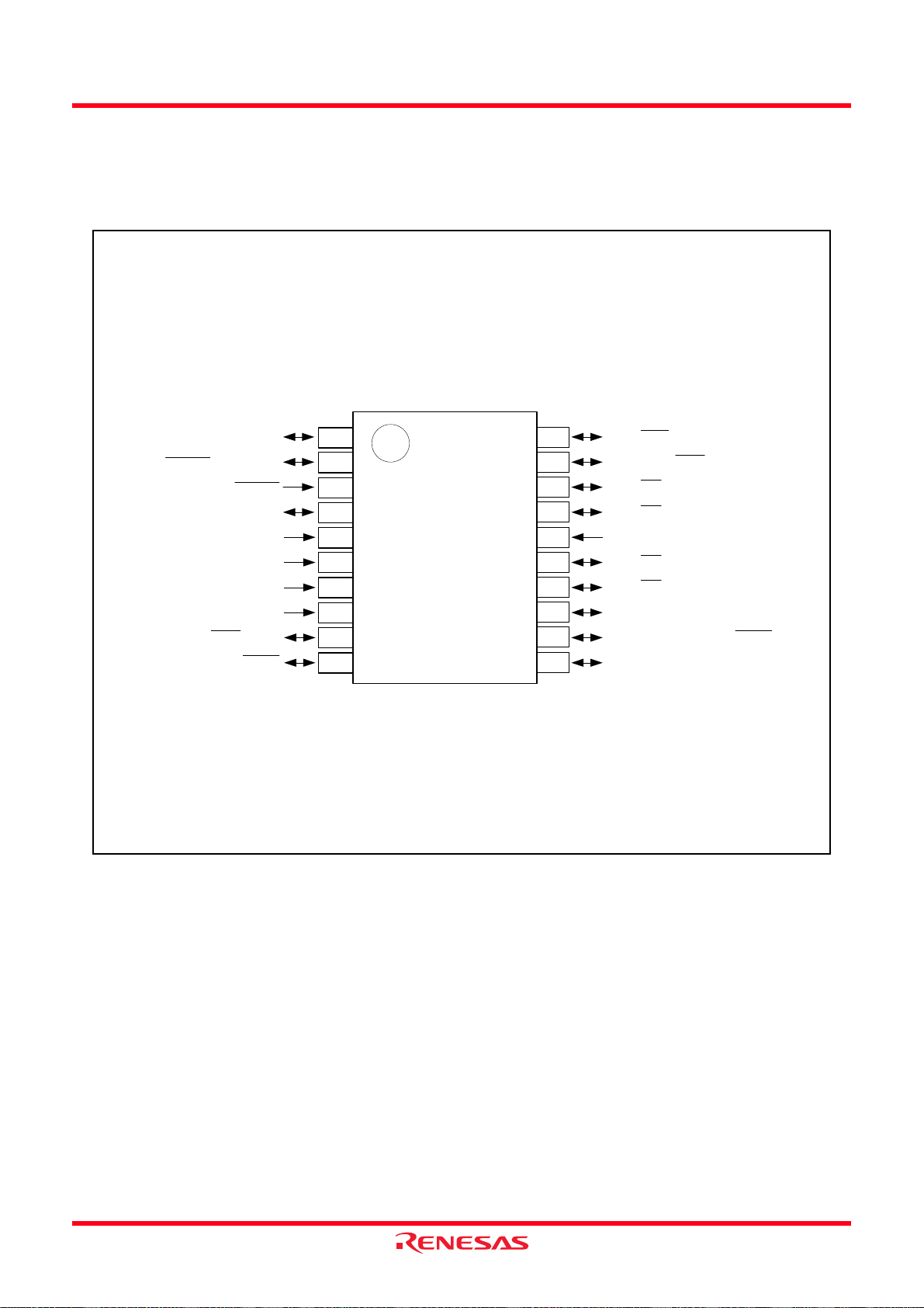
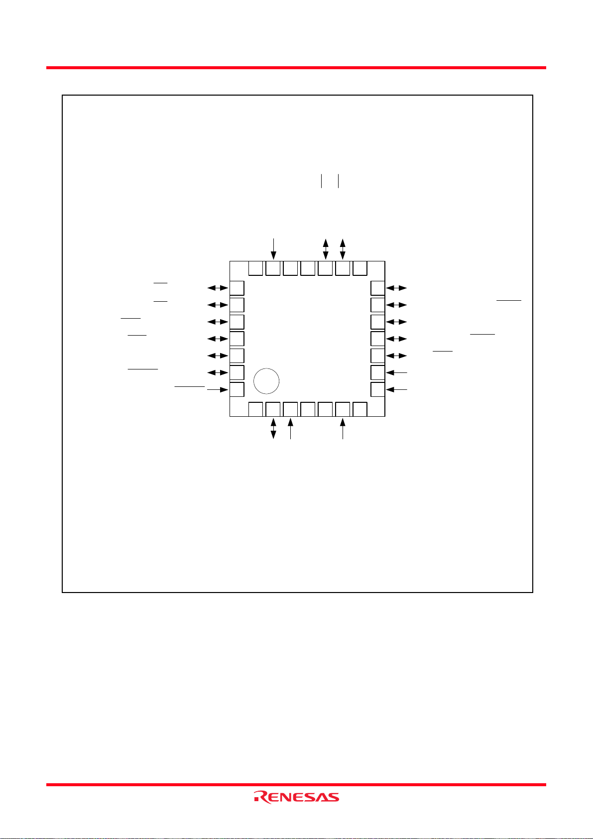
1.5 Pin Assignments
Figure 1.4 shows Pin Assignments for PLSP0020JB-A Package (Top View), Figure 1.5 shows Pin
Assignments for PRDP0020BA-A Package (Top View) and Figure 1.6 shows Pin Assignments for
PWQN0028KA-B Package (Top View).
PIN assignments (top view)
P3_5/SSCK/SCL/CMP1_2
P3_7/CNTR0/SSO/TXD1
RESET
XOUT/P4_7
VSS/AVSS
XIN/P4_6
VCC/AVCC
MODE
P4_5/INT0/RXD1
P1_7/CNTR00/INT10
1
2
3
(1)
4
5
6
7
8
9
10
R8C/1A Group
R8C/1B Group
20 P3_4/SCS/SDA/CMP1_1
19 P3_3/TCIN/INT3/SSI00/CMP1_0
18 P1_0/KI0/AN8/CMP0_0
17
16 P4_2/VREF
15 P1_2/KI2/AN10/CMP0_2
14 P1_3/KI3/AN11/TZOUT
13 P1_4/TXD0
12 P1_5/RXD0/CNTR01/INT11
11 P1_6/CLK0/SSI01
P1_1/KI1/AN9/CMP0_1
NOTE:
1. P4_7 is an input-only port.
Package: PLSP0020JB-A (20P2F-A)
Figure 1.4 Pin Assignments for PLSP0020JB-A Package (Top View)
Rev.1.10 Mar 17, 2006 Page 7 of 312
REJ09B0252-0110
Page 24
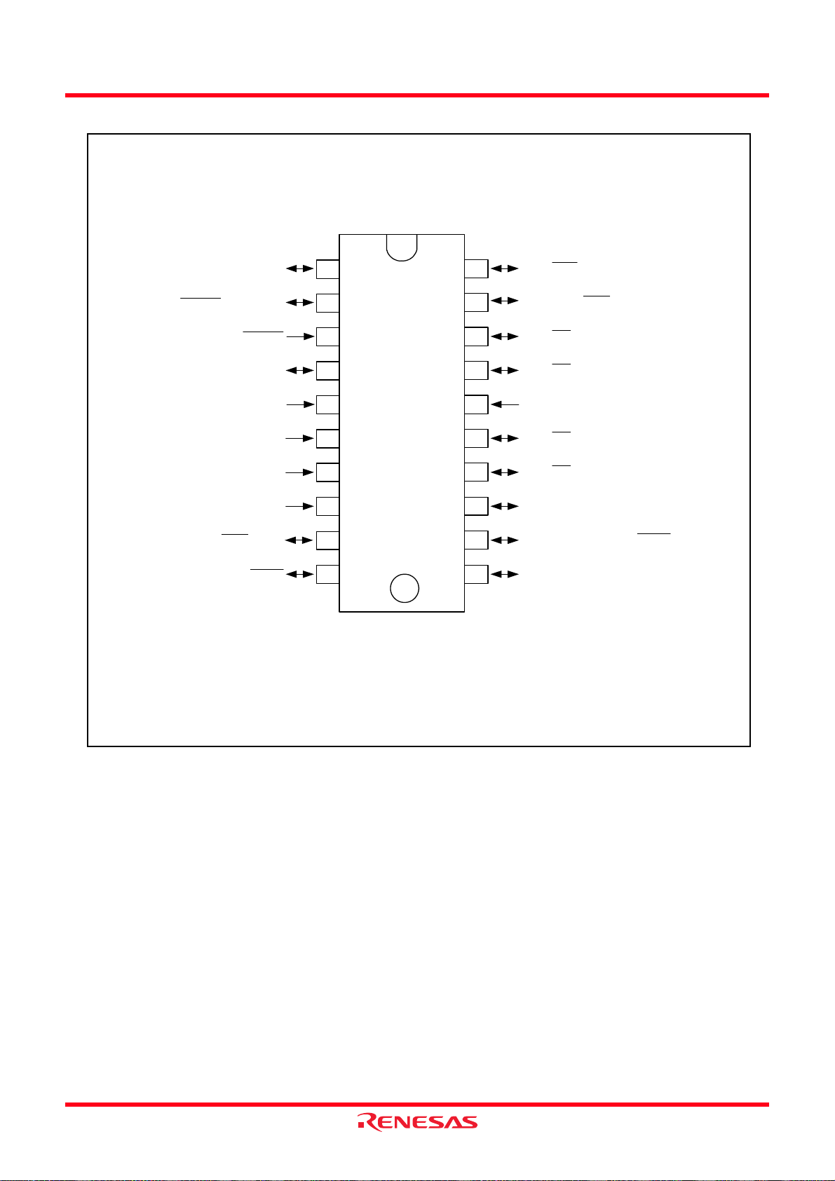
R8C/1A Group, R8C/1B Group 1. Overview
PIN assignments (top view)
P3_5/SSCK/SCL/CMP1_2
P3_7/CNTR0/SSO/TXD1
RESET
XOUT/P4_7
VSS/AVSS
XIN/P4_6
VCC/AVCC
MODE
P4_5/INT0/RXD1
P1_7/CNTR00/INT10
1
2
3
(1)
4
5
6
7
8
9
10
R8C/1B Group
NOTE:
1. P4_7 is an input-only port.
R8C/1A Group
20 P3_4/SCS/SDA/CMP1_1
19 P3_3/TCIN/INT3/SSI00/CMP1_0
18 P1_0/KI0/AN8/CMP0_0
17 P1_1/KI1/AN9/CMP0_1
16 P4_2/VREF
15 P1_2/KI2/AN10/CMP0_2
14 P1_3/KI3/AN11/TZOUT
13 P1_4/TXD0
12 P1_5/RXD0/CNTR01/INT11
11 P1_6/CLK0/SSI01
Package: PRDP0020BA-A (20P4B)
Figure 1.5 Pin Assignments for PRDP0020BA-A Package (Top View)
Rev.1.10 Mar 17, 2006 Page 8 of 312
REJ09B0252-0110
Page 25
R8C/1A Group, R8C/1B Group 1. Overview
PIN Assignment (top view)
P1_3/AN11/KI3/TZOUT
P1_2/AN10/KI2/CMP0_2
NC
NC
P4_2/VREF
NC
21 20 19 18 17 16 15
NC
P1_1/AN9/KI1/CMP0_1
P1_0/AN8/KI0/CMP0_0
P3_3/TCIN/INT3/SSI00/CMP1_0
P3_4/SCS/SDA/CMP1_1
P3_5/SSCK/SCL/CMP1_2
P3_7/CNTR0/SSO/TXD1
RESET
NOTES:
22
23
24
25
26
27
28
R8C/1A Group
R8C/1B Group
1 2 3 4 5 6 7
NC
(1)
XOUT/P4_7
NC
VSS/AVSS
1. P4_7 is a port for the input.
P1_4/TXD0
P1_5/RXD0/CNTR01/INT11
P1_6/CLK0/SSI01
P1_7/CNTR00/INT10
P4_5/INT0/RXD1
MODE
VCC/AVCC
NC
14
13
12
11
10
9
8
NC
XIN/P4_6
Package: PWQN0028KA-B(28PJW-B)
Figure 1.6 Pin Assignments for PWQN0028KA-B Package (Top View)
Rev.1.10 Mar 17, 2006 Page 9 of 312
REJ09B0252-0110
Page 26
R8C/1A Group, R8C/1B Group 1. Overview
1.6 Pin Functions
Table 1.5 lists Pin Functions, Table 1.6 lists Pin Name Information by Pin Number of PLSP0020JB-A,
PRDP0020BA-A Packages and Table 1.7 lists Pin Name Information by Pin Number of PWQN0028KAB Package.
Table 1.5 Pin Functions
Type Symbol I/O Type Description
Power Supply Input VCC, VSS I Apply 2.7 V to 5.5 V to the VCC pin.
Apply 0 V to the VSS pin.
Analog Power
Supply Input
Reset Input RESET
MODE MODE I Connect this pin to VCC via a resistor.
Main Clock Input XIN I These pins are provided for main clock generation
Main Clock Output XOUT O
INT
Interrupt INT0, INT1, INT3 I INT interrupt input pins
Key Input Interrupt KI0
Timer X CNTR0 I/O Timer X I/O pin
Timer Z TZOUT O Timer Z output pin
Timer C TCIN I Timer C input pin
Serial Interface CLK0 I/O Transfer clock I/O pin
Clock synchronous
serial I/O with chip
select (SSU)
2
I
C bus Interface
Reference V oltage
Input
A/D Converter AN8 to AN11 I Analog input pins to A/D converter
I/O Port P1_0 to P1_7,
Input Port P4_2, P4_6, P4_7 I Input-only ports
I: Input O: Output I/O: Input and output
AVCC, AVSS I Power supply for the A/D converter
Connect a capacitor between AVCC and AVSS.
I Input “L” on this pin resets the MCU.
circuit I/O. Connect a ceramic resonator or a
crystal oscillator between the XIN and XOUT pins.
To use an external clock, input it to the XIN pin and
leave the XOUT pin open.
to KI3 I Key input interrupt input pins
CNTR0
CMP0_0 to CMP0_2,
CMP1_0 to CMP1_2
RXD0, RXD1 I Serial data input pins
TXD0, TXD1 O Serial data output pins
SSI00, SSI01 I/O Data I/O pin.
SCS
SSCK I/O Clock I/O pin
SSO I/O Data I/O pin
SCL I/O Clock I/O pin
SDA I/O Data I/O pin
VREF I Reference voltage input pin to A/D converter
P3_3 to P3_5, P3_7,
P4_5
O Timer X output pin
O Timer C output pins
I/O Chip-select signal I/O pin
I/O CMOS I/O ports. Each port has an I/O select
direction register, allowing each pin in the port to
be directed for input or output individually.
Any port set to input can be set to use a pull-up
resistor or not by a program.
P1_0 to P1_3 also function as LED drive ports.
Rev.1.10 Mar 17, 2006 Page 10 of 312
REJ09B0252-0110
Page 27
R8C/1A Group, R8C/1B Group 1. Overview
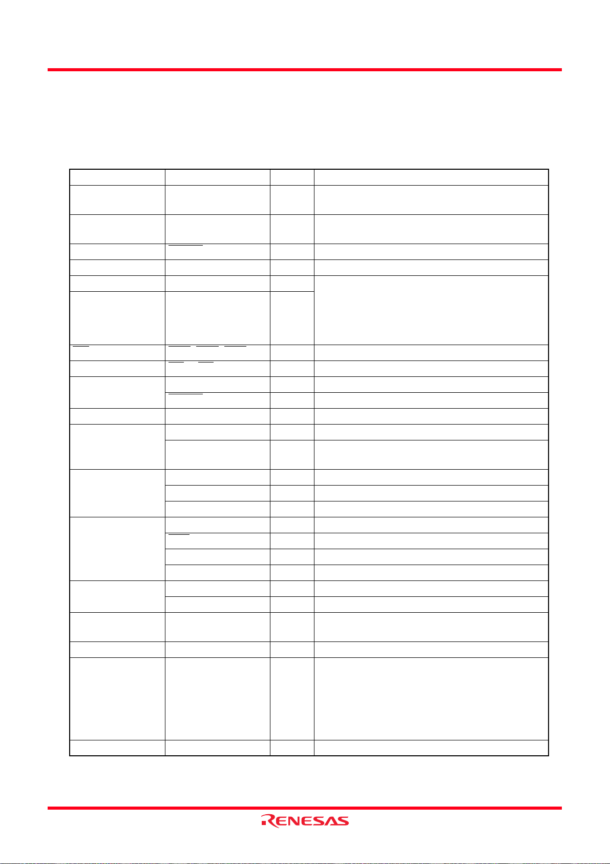
Table 1.6 Pin Name Information by Pin Number of PLSP0020JB-A, PRDP0020BA-A Packages
I/O Pin Functions for Peripheral Modules
Pin
Number
Control
Pin
Port
Interrupt Timer
Serial
Interface
Clock
Synchronous
Serial I/O with
2
I
C bus
Interface
A/D
Converter
Chip Select
1 P3_5 CMP1_2 SSCK SCL
2P3_7
3
RESET
CNTR0
TXD1 SSO
4XOUTP4_7
5 VSS/AVSS
6XINP4_6
7VCC/AVCC
8MODE
9P4_5
10 P1_7
INT0
INT10
CNTR00
RXD1
11 P1_6 CLK0 SSI01
12 P1_5
INT11
CNTR01 RXD0
13 P1_4 TXD0
14 P1_3
15 P1_2
KI3
KI2
TZOUT AN11
CMP0_2 AN10
16 VREF P4_2
17 P1_1
18 P1_0
19 P3_3
KI1
KI0
INT3
CMP0_1 AN9
CMP0_0 AN8
TCIN/
SSI00
CMP1_0
20 P3_4 CMP1_1
SCS
SDA
Rev.1.10 Mar 17, 2006 Page 11 of 312
REJ09B0252-0110
Page 28
R8C/1A Group, R8C/1B Group 1. Overview
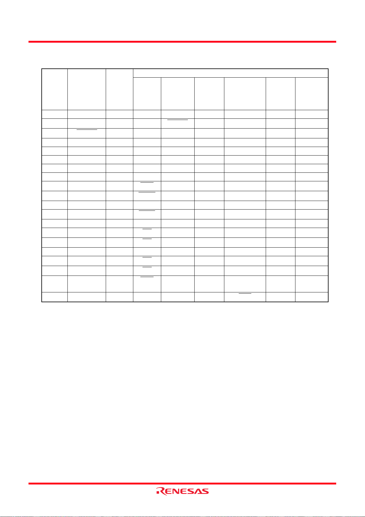
Table 1.7 Pin Name Information by Pin Number of PWQN0028KA-B Package
I/O Pin Functions for Peripheral Modules
Pin
Number
Control
Pin
Port
Interrupt Timer
Serial
Interface
Clock
Synchronous
Serial I/O with
2
I
C bus
Interface
A/D
Converter
Chip Select
1NC
2XOUTP4_7
3 VSS/AVSS
4NC
5NC
6XINP4_6
7NC
8VCC/AVCC
9MODE
10 P4_5
11 P1_7
INT0
INT10
CNTR00
RXD1
12 P1_6 CLK0 SSI01
13 P1_5
INT11
CNTR01 RX D0
14 P1_4 TXD0
15 NC
16 P1_3
17 P1_2
KI3
KI2
TZOUT AN11
CMP0_2 AN10
18 NC
19 NC
20 VREF P4_2
21 NC
22 P1_1
23 P1_0
24 P3_3
KI1
KI0
INT3
25 P3_4 CMP1_1
CMP0_1 AN9
CMP0_0 AN8
TCIN/CMP1_0 SSI00
SCS
SDA
26 P3_5 CMP1_2 SSCK SCL
27 P3_7
28
RESET
CNTR0
TXD1 SSO
Rev.1.10 Mar 17, 2006 Page 12 of 312
REJ09B0252-0110
Page 29
R8C/1A Group, R8C/1B Group 2. Central Processing Unit (CPU)
2. Central Processing Unit (CPU)
Figure 2.1 shows the CPU Registers. The CPU contains 13 registers. R0, R1, R2, R3, A0, A1, and FB
configure a register bank. There are two sets of register bank.
b31
R2
R3
b15 b8b7
R0H (high-order of R0)
R1H (high-order of R1) R1L (low-order of R1)
R0L (low-order of R0)
R2
R3
A0
A1
FB
b15b19
INTBH
The 4 high order bits of INTB are INTBH and
the 16 low bits of INTB are INTBL.
b19
INTBL
PC
b15
USP
ISP
SB
b0
Data registers
Address registers
Frame base register
b0
Interrupt table register
b0
Program counter
b0
User stack pointer
Interrupt stack pointer
Static base register
(1)
(1)
(1)
b15
IPL
NOTE:
1. These registers comprise a register bank. There are two register banks.
Figure 2.1 CPU Register
b15
b0
FLG
b8
b7
b0
C
DZSBOIU
Flag register
Carry flag
Debug flag
Zero flag
Sign flag
Register bank select flag
Overflow flag
Interrupt enable flag
Stack pointer select flag
Reserved bit
Processor interrupt priority level
Reserved bit
Rev.1.10 Mar 17, 2006 Page 13 of 312
REJ09B0252-0110
Page 30

R8C/1A Group, R8C/1B Group 2. Central Processing Unit (CPU)
2.1 Data Registers (R0, R1, R2, and R3)
R0 is a 16-bit register for transfer, arithmetic, and logic operations. T he same applies to R1 to R3. R0
can be split into high-order bits (R0H) and low-order bits (R0L) to be used separately as 8-bit data
registers. R1H and R1L are analogous to R0H and R0L. R2 can be combined with R0 and used as a 32bit data register (R2R0). R3R1 is analogous to R2R0.
2.2 Address Registers (A0 and A1)
A0 is a 16-bit register for address register indirect addressing and address register relative addressing.
It is also used for transfer and arithmetic and logic operation s. A1 is analogous to A0. A1 can be
combined with A0 and used as a 32-bit address register (A1A0).
2.3 Frame Base Register (FB)
FB is a 16-bit register for FB relative addressing.
2.4 Interrupt Table Register (INTB)
INTB is a 20-bit register that indicates the start address of an interrupt vector table.
2.5 Program Counter (PC)
PC is 20 bits wide indicates the address of the next instruction to be executed.
2.6 User Stack Pointer (USP) and Interrupt Stack Pointer (ISP)
The stack pointer (SP), USP, and ISP, are each 16 bits wide. The U flag of FLG is used to switch
between USP and ISP.
2.7 Static Base Register (SB)
SB is a 16-bit register for SB relative addressing.
2.8 Flag Register (FLG)
FLG is an 11-bit register indicating the CPU state.
2.8.1 Carry Flag (C)
The C flag retains a carry, borrow, or shift-out bits that have been generated by the arithmetic and
logic unit.
2.8.2 Debug Flag (D)
The D flag is for debugging only. Set it to 0.
2.8.3 Zero Flag (Z)
The Z flag is set to 1 when an arithmetic operation results in 0; otherwise to 0.
2.8.4 Sign Flag (S)
The S flag is set to 1 when an arithmetic operation results in a negative value; otherwise to 0.
2.8.5 Register Bank Select Flag (B)
Register bank 0 is selected when the B flag is 0. Register bank 1 is selected when this flag is set to 1.
2.8.6 Overflow Flag (O)
The O flag is set to 1 when the operation results in an overflow; otherwise to 0.
Rev.1.10 Mar 17, 2006 Page 14 of 312
REJ09B0252-0110
Page 31

R8C/1A Group, R8C/1B Group 2. Central Processing Unit (CPU)
2.8.7 Interrupt Enable Flag (I)
The I flag enables maskable interrupts.
Interrupts are disabled when the I flag is set to 0, and are enabled when the I flag is set to 1. The I
flag is set to 0 when an interrupt request is acknowledged.
2.8.8 Stack Pointer Select Flag (U)
ISP is selected when the U flag is set to 0; USP is selected when the U flag is set to 1.
The U flag is set to 0 when a hardware interrupt request is acknowledged or the INT instruction of
software interrupt numbers 0 to 31 is executed.
2.8.9 Processor Interrupt Priority Level (IPL)
IPL is 3 bits wide, assigns processor interrupt priority levels from level 0 to level 7.
If a requested interrupt has higher priority than IPL, the interrupt is enabled.
2.8.10 Reserved Bit
If necessary, set to 0. When read, the content is undefined.
Rev.1.10 Mar 17, 2006 Page 15 of 312
REJ09B0252-0110
Page 32

R8C/1A Group, R8C/1B Group 3. Memory
3. Memory
3.1 R8C/1A Group
Figure 3.1 is a Memory Map of R8C/1A Group. The R8C/1A Group has 1 Mbyte of address space from
addresses 00000h to FFFFFh.
The internal ROM is allocated lower addresses, beginning with address 0FFFFh. For exam ple, a 16Kbyte internal ROM area is allocated addresses 0C000h to 0FFFFh.
The fixed interrupt vector table is allocated addresses 0FFDCh to 0FFFFh. They store the starting
address of each interrupt routine.
The internal RAM is allocated higher addresses, beginning with a ddress 00400h. For example, a 1Kbyte internal RAM area is allocated addresses 00400h to 007FFh. The internal RAM is used not only
for storing data but also for calling subroutines and as stacks when interrupt requests are
acknowledged.
Special function registers (SFRs) are allocated addresses 00000h to 002FFh. The peripheral function
control registers are allocated here. All addresses within the SFR, which have nothing allocated are
reserved for future use and cannot be accessed by users.
00000h
(See 4. Special Function
002FFh
00400h
0XXXXh
0YYYYh
0FFFFh
FFFFFh
NOTE:
1. The blank regions are reserved. Do not access locations in these regions.
R5F211A4SP, R5F211A4DSP, R5F211A4DD, R5F211A4NP
R5F211A3SP, R5F211A3DSP, R5F211A3DD, R5F211A3NP
R5F211A2SP, R5F211A2DSP, R5F211A2DD, R5F211A2NP
R5F211A1SP, R5F211A1DSP, R5F211A1DD
SFR
Registers (SFRs))
Internal RAM
Internal ROM
Expanded area
Part Number
0FFDCh
Watchdog timer•oscillation stop detection•voltage monitor 2
0FFFFh
Internal ROM Internal RAM
Size
16 Kbytes
12 Kbytes
8 Kbytes
4 Kbytes
Undefined instruction
Overflow
BRK instruction
Address match
Single step
Address break
(Reserved)
Address
0YYYYh
0C000h
0D000h
0E000h
0F000h
Reset
768 bytes
512 bytes
384 bytes
Size
1 Kbyte
Address
0XXXXh
007FFh
006FFh
005FFh
0057Fh
Figure 3.1 Memory Map of R8C/1A Group
Rev.1.10 Mar 17, 2006 Page 16 of 312
REJ09B0252-0110
Page 33

R8C/1A Group, R8C/1B Group 3. Memory
3.2 R8C/1B Group
Figure 3.2 is a Memory Map of R8C/1B Group. The R8C/1B Group has 1 Mbyte of address space from
addresses 00000h to FFFFFh.
The internal ROM (program ROM) is allocated lower addresses, beginning with address 0FFFFh. For
example, a 16-Kbyte internal ROM area is allocated addresses 0C000h to 0FFFFh.
The fixed interrupt vector table is allocated addresses 0FFDCh to 0FFFFh. They store the starting
address of each interrupt routine.
The internal ROM (data flash) is allocated addresses 02400h to 02BFFh.
The internal RAM is allocated higher addresses beginning with address 00400h. For example, a 1Kbyte internal RAM area is allocated addresses 00400h to 007FFh. The internal RAM is used not only
for storing data but also for calling subroutines and as stacks when interrupt requests are
acknowledged.
Special function registers (SFRs) are allocated addresses 00000h to 002FFh. The peripheral function
control registers are allocated here. All addresses within the SFR, which have nothing allocated are
reserved for future use and cannot be accessed by users.
00000h
(See 4. Special Function
002FFh
00400h
0XXXXh
02400h
02BFFh
0YYYYh
0FFFFh
FFFFFh
NOTES:
1. Data flash block A (1 Kbyte) and B (1 Kbyte) are shown.
2. The blank regions are reserved. Do not access locations in these regions.
R5F211B4SP, R5F211B4DSP, R5F211B4DD, R5F211B4NP
R5F211B3SP, R5F211B3DSP, R5F211B3DD, R5F211B3NP
R5F211B2SP, R5F211B2DSP, R5F211B2DD, R5F211B2NP
R5F211B1SP, R5F211B1DSP, R5F211B1DD
SFR
Registers (SFRs))
Internal RAM
Internal ROM
(data Flash)
Internal ROM
(program ROM)
Expanded area
Part Number
(1)
0FFDCh
0FFFFh
Undefined instruction
Overflow
BRK instruction
Address match
Watchdog timer • oscillation stop detection • voltage monitor 2
Internal ROM Internal RAM
Size
16 Kbytes
12 Kbytes
8 Kbytes
4 Kbytes
Address break
Address
0YYYYh
0C000h
0D000h
0E000h
0F000h
Single step
(Reserved)
Reset
Size
1 Kbyte
768 bytes
512 bytes
384 bytes
Address
0XXXXh
007FFh
006FFh
005FFh
0057Fh
Figure 3.2 Memory Map of R8C/1B Group
Rev.1.10 Mar 17, 2006 Page 17 of 312
REJ09B0252-0110
Page 34

R8C/1A Group, R8C/1B Group 4. Special Function Registers (SFRs)
4. Special Function Registers (SFRs)
An SFR (special function register) is a control register for a peripheral function. Tables 4.1 to 4.4 list the
special function registers.
Table 4.1 SFR Information (1)
Address Register Symbol After reset
0000h
0001h
0002h
0003h
0004h Processor Mode Register 0 PM0 00h
0005h Processor Mode Register 1 PM1 00h
0006h System Clock Control Register 0 CM0 0110 1000b
0007h System Clock Control Register 1 CM1 00100000b
0008h
0009h Address Match Interrupt Enable Register AIER 00h
000Ah Protect Register PRCR 00h
000Bh
000Ch Oscillation Stop Detection Register OCD 00000100b
000Dh Watchdog Timer Reset Register WDTR XXh
000Eh Watchdog Timer Start Register WDTS XXh
000Fh Watchdog Timer Control Register WDC 000XXXXXb
0010h Address Match Interrupt Register 0 RMAD0 00h
0011h 00h
0012h X0h
0013h
0014h Address Match Interrupt Register 1 RMAD1 00h
0015h 00h
0016h X0h
0017h
0018h
0019h
001Ah
001Bh
001Ch Count Source Protection Mode Register CSPR 00h
001Dh
001Eh
001Fh
0020h High-Speed On-Chip Oscillator Control Register 0 HRA0 00h
0021h High-Speed On-Chip Oscillator Control Register 1 HRA1 When shipping
0022h High-Speed On-Chip Oscillator Control Register 2 HRA2 00h
0023h
INT0
Input Filter Select Register
(1)
INT0F 00h
002Ah
002Bh
002Ch
002Dh
002Eh
002Fh
0030h
0031h
0032h
0033h
0034h
0035h
0036h
0037h
0038h
0039h
003Ah
003Bh
003Ch
003Dh
003Eh
003Fh
Voltage Detection Register 1
Voltage Detection Register 2
Voltage Monitor 1 Circuit Control Regist er
Voltage Monitor 2 Circuit Control Regist er
(2)
(2)
(2)
(5)
X: Undefined
NOTES:
1. The blank regions are reserved. Do not access locations in these regions.
2. Software reset, watchdog timer reset, and voltage monitor 2 reset do not affect this register.
3. After hardware reset.
4. After power-on reset or voltage monitor 1 reset.
5. Software reset, watchdog timer reset, and voltage monitor 2 reset do not affect b2 and b3.
VCA1 00001000b
VCA2
VW1C
VW2C 00h
(3)
00h
01000000b
0000X000b
0100X001b
(4)
(3)
(4)
Rev.1.10 Mar 17, 2006 Page 18 of 312
REJ09B0252-0110
Page 35

R8C/1A Group, R8C/1B Group 4. Special Function Registers (SFRs)
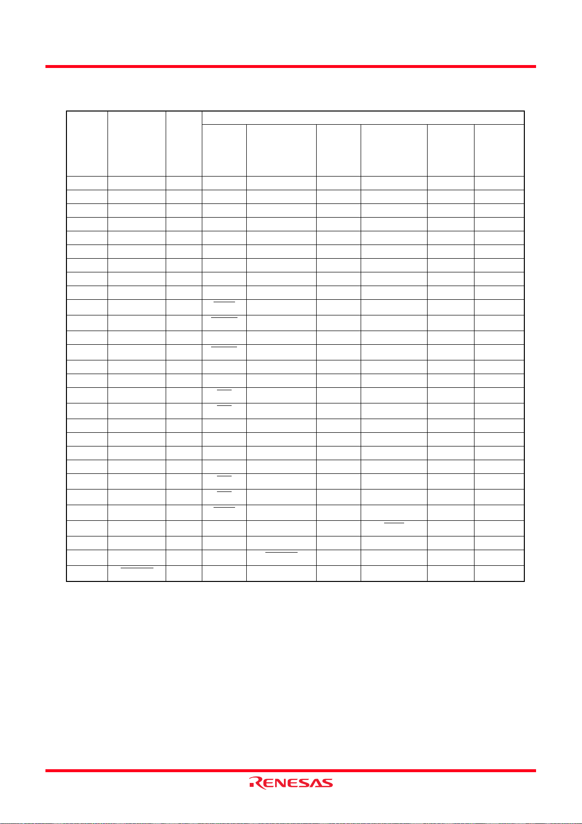
Table 4.2 SFR Information (2)
Address Register Symbol After reset
0040h
0041h
0042h
0043h
0044h
0045h
0046h
0047h
0048h
0049h
004Ah
004Bh
004Ch
004Dh Key Input Interrupt Control Register KUPIC XXXXX000b
004Eh A/D Conversion Interrupt Control Register ADIC XXXXX000b
004Fh
0050h Compare 1 Interrupt Control Register CMP1IC XXXXX000b
0051h UART0 Transmit Interrupt Control Register S0TIC XXXXX000b
0052h UART0 Receive Interrupt Control Register S0RIC XXXXX000b
0053h UART1 Transmit Interrupt Control Register S1TIC XXXXX000b
0054h UART1 Receive Interrupt Control Register S1RIC XXXXX000b
0055h
0056h Timer X Interrupt Control Register TXIC XXXXX000b
0057h
0058h Timer Z Interrupt Control Register TZIC XXXXX000b
0059h INT1 Interrupt Control Register INT1IC XXXXX000b
005Ah INT3 Interrupt Control Register INT3IC XXXXX000b
005Bh Timer C Interrupt Control Register TCIC XXXXX000b
005Ch Compare 0 Interrupt Control Register CMP0IC XXXXX000b
005Dh INT0 Interrupt Control Register INT0IC XX00X000b
005Eh
005Fh
0060h
0061h
0062h
0063h
0064h
0065h
0066h
0067h
0068h
0069h
006Ah
006Bh
006Ch
006Dh
006Eh
006Fh
0070h
0071h
0072h
0073h
0074h
0075h
0076h
0077h
0078h
0079h
007Ah
007Bh
007Ch
007Dh
007Eh
007Fh
SSU/IIC Interrupt Control Register
(1)
(2)
SSUAIC/IIC2AIC XXXXX000b
X: Undefined
NOTES:
1. The blank regions are reserved. Do not access locations in these regions.
2. Selected by the IICSEL bit in the PMR register.
Rev.1.10 Mar 17, 2006 Page 19 of 312
REJ09B0252-0110
Page 36

R8C/1A Group, R8C/1B Group 4. Special Function Registers (SFRs)
Table 4.3 SFR Information (3)
Address Register Symbol After reset
0080h Timer Z Mode Register TZMR 00h
0081h
0082h
0083h
0084h Timer Z Waveform Output Control Register PUM 00h
0085h Prescaler Z Register PREZ FFh
0086h Timer Z Secondary Register TZSC FFh
0087h Timer Z Primary Register TZPR FFh
0088h
0089h
008Ah Timer Z Output Control Register TZOC 00h
008Bh Timer X Mode Register TXMR 00h
008Ch Prescaler X Register PREX FFh
008Dh Timer X Register TX FFh
008Eh Timer Count Source Setting Register TCSS 00h
008Fh
0090h Timer C Register TC 00h
0091h 00h
0092h
0093h
0094h
0095h
0096h External Input Enable Register INTEN 00h
0097h
0098h Key Input Enable Register KIEN 00h
0099h
009Ah Timer C Control Register 0 TCC0 00h
009Bh Timer C Control Register 1 TCC1 00h
009Ch Capture, Compare 0 Register TM0
009Dh
009Eh Compare 1 Register TM1 FFh
009Fh FFh
00A0h UART0 Transmit/Receive Mode Register U0MR 00h
00A1h UART0 Bit Rate Generator U0BRG XXh
00A2h UART0 Transmit Buffer Register U0TB XXh
00A3h XXh
00A4h UART0 Transmit/Receive Control Register 0 U0C0 00001000b
00A5h UART0 Transmit/Receive Control Register 1 U0C1 00000010b
00A6h UART0 Receive Buffer Register U0RB XXh
00A7h XXh
00A8h UART1 Transmit/Receive Mode Register U1MR 00h
00A9h UART1 Bit Rate Generator U1BRG XXh
00AAh UART1 Transmit Buffer Register U1TB XXh
00ABh XXh
00ACh UART1 Transmit/Receive Control Register 0 U1C0 00001000b
00ADh UART1 Transmit/Receive Control Register 1 U1C1 00000010b
00AEh UART1 Receive Buffer Register U1RB XXh
00AFh XXh
00B0h UART Transmit/Receive Control Register 2 UCON 00h
00B1h
00B2h
00B3h
00B4h
00B5h
00B6h
00B7h
00B8h
00B9h
00BAh
00BBh
00BCh
00BDh
00BEh
00BFh
SS Control Register H / IIC bus Control Register 1
SS Control Register L / IIC bus Control Register 2
SS Mode Register / IIC bus Mode Register
SS Enable Register / IIC bus Interrupt Enable Register
SS Status Register / IIC bus Status Register
SS Mode Register 2 / Slave Address Register
SS Transmit Data Register / IIC bus Transmit Data Register
SS Receive Data Register / IIC bus Receive Data Register
(1)
0000h
FFFFh
(4)
(4)
(4)
(4)
(4)
(4)
(4)
(4)
SSCRH / ICCR1 00h
SSCRL / ICCR2 01111101b
SSMR / ICMR 00011000b
SSER / ICIER 00h
SSSR / ICSR 00h / 0000X000b
SSMR2 / SAR 00h
SSTDR / ICDRT FFh
SSRDR / ICDRR FFh
X: Undefined
NOTES:
1. The blank regions are reserved. Do not access locations in these regions.
2. In input capture mode.
3. In output compare mode.
4. Selected by the IICSEL bit in the PMR register.
(2)
(3)
Rev.1.10 Mar 17, 2006 Page 20 of 312
REJ09B0252-0110
Page 37

R8C/1A Group, R8C/1B Group 4. Special Function Registers (SFRs)
Table 4.4 SFR Information (4)
Address Register Symbol After reset
00C0h A/D Register AD XXh
00C1h XXh
00C2h
00C3h
00C4h
00C5h
00C6h
00C7h
00C8h
00C9h
00CAh
00CBh
00CCh
00CDh
00CEh
00CFh
00D0h
00D1h
00D2h
00D3h
00D4h A/D Control Register 2 ADCON2 00h
00D5h
00D6h A/D Control Register 0 ADCON0 00000XXXb
00D7h A/D Control Register 1 ADCON1 00h
00D8h
00D9h
00DAh
00DBh
00DCh
00DDh
00DEh
00DFh
00E0h
00E1h Port P1 Register P1 XXh
00E2h
00E3h Port P1 Direction Register PD1 00h
00E4h
00E5h Port P3 Register P3 XXh
00E6h
00E7h Port P3 Direction Register PD3 00h
00E8h Port P4 Register P4 XXh
00E9h
00EAh Port P4 Direction Register PD4 00h
00EBh
00ECh
00EDh
00EEh
00EFh
00F0h
00F1h
00F2h
00F3h
00F4h
00F5h
00F6h
00F7h
00F8h Port Mode Register PMR 00h
00F9h
00FAh
00FBh
00FCh Pull-Up Control Register 0 PUR0 00XX0000b
00FDh Pull-Up Control Register 1 PUR1 XXXXXX0Xb
00FEh Port P1 Drive Capacity Control Register DRR 00h
00FFh Timer C Output Control Register TCOUT 00h
01B3h Flash Memory Control Register 4 FMR4 01000000b
01B4h
01B5h Flash Memory Control Register 1 FMR1 1000000Xb
01B6h
01B7h Flash Memory Control Register 0 FMR0 00000001b
0FFFFh Optional Function Select Register OFS (2)
(1)
X: Undefined
NOTES:
1. Blank regions, 0100h to 01B2h and 01B8h to 02FFh are all reserved. Do not access locations in these regions.
2. The OFS register cannot be changed by a user program. Use a flash programmer to write to it.
Rev.1.10 Mar 17, 2006 Page 21 of 312
REJ09B0252-0110
Page 38

R8C/1A Group, R8C/1B Group 5. Programmable I/O Ports
5. Programmable I/O Ports
There are 13 programmable Input/Output ports (I/O ports) P1, P3_3 to P3_5, P3_7, and P4_5. 4_2 can be used as an
input-only port. Also, P4_6 and P4_7 can be used as input-only ports if the main clock oscillation circuit is not used.
Table 5.1 lists an Overview of Programmable I/O Ports.
Table 5.1 Overview of Programmable I/O Ports
Ports I/O Type of Output I/O Setting
P1 I/O CMOS3 state Set per bit
P3_3, P4_5 I/O CMOS3 state Set per bit
P3_4, P3_5, P3_7 I/O CMOS3 state Set per bit
(3)
P4_2, P4_6, P4_7
NOTES:
1. In input mode, whether an internal pull-up resistor is connected or not can be selected by registers PUR0 and
PUR1.
2. These ports can be used as the LED drive port by setting the DRR register to 1 (high).
3. When the main clock oscillation circuit is not used, P4_6 and P4_7 can be used as input -only ports.
I (No output function) None None None
Internal Pull-Up
Resistor
Set every 4 bits
Set every bit
Set every 3 bits
(1)
(1)
(1)
5.1 Functions of Programmable I/O Ports
The PDi_j (j=0 to 7) bit in the PDi (i=1, 3, and 4) register controls I/O of ports P1, P3_3 to P3_5, P3_7, and P4_5.
The Pi register consists of a port la tch to ho ld output data and a circuit to read pin states. Figures 5.1 to 5.3 show the
Configurations of Programmable I/O Ports.
Table 5.2 lists the Functions of Programmable I/O Ports. Also, Figure 5.5 shows Registers PD1, PD3, and PD4.
Figure 5.6 shows Registers P1 and P3, Figure 5.9 shows Registers PUR0 and PUR1 and Figure 5.10 shows the
DRR Register.
Drive Capacity
Selection
Set every bit
P1_0 to P1_3
None
None
(2)
of
Table 5.2 Functions of Programmable I/O Ports
Operation when
Accessing
Pi Register
Reading Read pin input level Read the port latch
Writing Write to the port latch Write to the port latch. The value written to the
NOTE:
1. Nothing is assigned to bits PD3_0 to PD3_2, PD3_6, PD4_0 to PD4_4, PD4_6, and PD4_7.
When PDi_j Bit is Set to 0 (Input Mode) When PDi_j Bit is Set to 1 (Output Mode)
Value of PDi_j Bit in PDi Register
port latch is output from the pin.
(1)
5.2 Effect on Peripheral Functions
Programmable I/O ports function as I/O ports for peripheral functions (Refer to T able 1.6 Pin Name Information by
Pin Number of PLSP0020JB-A, PRDP0020BA-A Packages). Table 5.3 lists the Settings of PDi_j Bit when
Functioning as I/O Ports for Peripheral Functions. Refer to the description of each function for information on how
to set peripheral functions.
Table 5.3 Settings of PDi_j Bit when Functioning as I/O Ports for Peripheral Functions
I/O of Peripheral Functions PDi_j Bit Settings for Shared Pin Functions
Input Set this bit to 0 (input mode).
Output This bit can be set to either 0 or 1 (output regardless of the port setting).
5.3 Pins Other than Programmable I/O Ports
Figure 5.4 shows the Configuration of I/O Pins.
Rev.1.10 Mar 17, 2006 Page 22 of 312
REJ09B0252-0110
Page 39

R8C/1A Group, R8C/1B Group 5. Programmable I/O Ports
P1_0 to P1_3
Output from individual peripheral function
Data bus
P1_4
Output from individual peripheral function
Data bus
Pull-up selection
Direction
register
1
Port latch
Input to individual peripheral function
Analog input
Pull-up selection
Direction
register
1
Port latch
(Note 1)
Drive capacity selection
P1_5
Direction
register
Data bus
Input to individual peripheral function
NOTE :
1. symbolizes a parasitic diode.
Ensure the input voltage to each port will not exceed VCC.
Port latch
(Note 1)
Pull-up selection
(Note 1)
Figure 5.1 Configuration of Programmable I/O Ports (1)
Rev.1.10 Mar 17, 2006 Page 23 of 312
REJ09B0252-0110
Page 40

R8C/1A Group, R8C/1B Group 5. Programmable I/O Ports
P1_6, P1_7
Data bus
P3_3
Pull-up selection
Direction
register
Output from individual peripheral function
Port latch
Input to individual peripheral function
Pull-up selection
Direction
register
Output from individual peripheral function
Data bus
Port latch
1
(Note 1)
1
Input to individual peripheral function
P3_4, P3_5, P3_7
Output from individual peripheral function
Data bus
Input to individual peripheral function
Direction
register
Port latch
(Note 1)
Digital
filter
Pull-up selection
1
(Note 1)
NOTE :
1. symbolizes a parasitic diode.
Ensure the input voltage to each port will not exceed VCC.
Figure 5.2 Configuration of Programmable I/O Ports (2)
Rev.1.10 Mar 17, 2006 Page 24 of 312
REJ09B0252-0110
Page 41

R8C/1A Group, R8C/1B Group 5. Programmable I/O Ports
P4_2
Vref of A/D converter
(Note 4)
Data bus
P4_5
Data bus
Input to individual peripheral function
P4_6/XIN
Direction
register
Port latch
Pull-up selection
(Note 4)
Digital
filter
Data bus
Clocked inverter
(1)
(Note 2)
P4_7/XOUT
Data bus
NOTES:
1. When CM05 = 1, CM10 = 1, or CM13 = 0, the clocked inverter is cut off.
2. When CM10 = 1 or CM13 = 0, the feedback resistor is disconnected.
3. When CM05 = CM13 = 1 or CM10 = CM13 = 1, this pin is pulled up.
4. symbolizes a parasitic diode.
Ensure the input voltage to each port does not exceed VCC.
Figure 5.3 Configuration of Programmable I/O Ports (3)
Rev.1.10 Mar 17, 2006 Page 25 of 312
REJ09B0252-0110
(Note 4)
(Note 3)
(Note 4)
Page 42

R8C/1A Group, R8C/1B Group 5. Programmable I/O Ports
MODE
MODE signal input
(Note 1)
RESET
RESET signal input
(Note 1)
NOTE :
1. symbolizes a parasitic diode.
Ensure the input voltage to each port will not exceed VCC.
Figure 5.4 Configuration of I/O Pins
Rev.1.10 Mar 17, 2006 Page 26 of 312
REJ09B0252-0110
Page 43

R8C/1A Group, R8C/1B Group 5. Programmable I/O Ports
Port P i Di rect i on Regi ster (i = 1, 3 , 4)
b7 b6 b5 b4 b3 b2
b1 b0
(1, 2)
Symbol Address After Reset
PD1
PD3
PD4
00E3h 00h
00E7h 00h
00EAh 00h
Bit Symbol Bit Name Function RW
PDi_0
PDi_1
PDi_2
Port Pi0 direction bit
Port Pi1 direction bit
Port Pi2 direction bit
PDi_3 Port Pi3 di rection bit
PDi_4
PDi_5
PDi_6
Port Pi4 direction bit
Port Pi5 direction bit
Port Pi6 direction bit RW
PDi_7 Port Pi7 di rection bit RW
NOTES :
Bits PD3_0 to PD3_2, and PD3_6 in the PD3 register are unavailable on this MCU.
1.
I f it is necessary to set bits PD3_0 to PD3_2, and PD3_6, set to 0 (input mode). When read, the content is 0.
Bits PD4_0 to PD4_4, PD4_6, and PD4_7 in the PD4 register are unavailable on this MCU. If it is necessary to set bits
2.
PD4_0 to PD4_4, PD4_6, and PD4_7, set to 0 (input mode). When read, the content is 0.
Figure 5.5 Registers PD1, PD3, and PD4
(functions as an input port)
1 : Output mode
(functions as an output port)
RW0 : Input mode
RW
RW
RW
RW
RW
Port P i Regi st er (i = 1, 3 )
b7 b6 b5 b4 b0
b3 b2 b1
(1)
Symbol Address After Reset
P1
P3
Bit Symbol Bit Name Function RW
Pi_0
Pi_1
Pi_2
Pi_3
Pi_4
Pi_5
Pi_6
Pi_7
Port Pi1 bit
Port Pi2 bit
Port Pi3 bit
Port Pi4 bit
Port Pi5 bit
Port Pi6 bit RW
Port Pi7 bit
NOTE :
Bits P3_0 to P3_2, and P3_6 in the P3 register are unavailable on this MCU.
1.
I f it is necessary to set bits P3_0 to P3_2, and P3_6, set to 0 (“L” level). When read, the content is 0.
Figure 5.6 Registers P1 and P3
00E1h Undefined
00E5h Undefined
The pi n level of any I/O port which is set
to input mode can be read by reading the
corresponding bit in this register. The pin
level of any I/O port which is set to output
mode can be controlled by w riting to the
corresponding bit in this register.
0 : “L” level
1 : “H” level
(1)
RWPort Pi0 bit
RW
RW
RW
RW
RW
RW
Rev.1.10 Mar 17, 2006 Page 27 of 312
REJ09B0252-0110
Page 44

R8C/1A Group, R8C/1B Group 5. Programmable I/O Ports
r
Port P 4 Regis ter
b7 b6 b5 b4 b3 b2 b1
b0
Symbol Address After Reset
P4
Bit Symbol Bit N ame Function R W
—
(b1-b0)
P4_2
—
(b4-b3)
P4_5
Nothing is assigned. If necessary, set to 0 (“L” level).
When read, the content is 0.
Port P4_2 bit
Nothing is assigned. If necessary, set to 0 (“L” level).
When read, the content is 0.
Port P4_5 bit
00E8h U ndefined
The level of the pin can be read by reading the bit.
0 : “L” level
1 : “H” level
The pi n level of any I/O port w hich is set to input mode
can be read by reading the corresponding bit in this
register. The pin level of any I/O port w hich is set to
output mode can be controlled by writing to the
corresponding bit in this register.
0 : “L” level
1 : “H” level
—
R
—
RW
P4_6
P4_7
Figure 5.7 P4 Register
Port Mo de Regi st e
b7 b6 b5 b4 b3 b20b10b0
000
0
Symbol Address After Reset
PMR
Bit Symbol Bit Name Function RW
—
(b2-b0)
SSIS EL
—
(b6-b4)
IICSEL RW
Port P4_6 bit
Port P4_7 bit
00F8h 00h
Res erved bits
SSI signal pin select bit
Res erved bits
2
C bus sw itch bit
SSU / I
The level of the pin can be read by reading the bit.
0 : “L” level
1 : “H” level
Set to 0.
0 : P3_3 pin is used for SSI00 pin.
1 : P1_6 pin is used for SSI01 pin.
Set to 0.
0 : Selects SSU function.
1 : Selects I
2
C bus function.
R
R
RW
RW
RW
Figure 5.8 PMR Register
Rev.1.10 Mar 17, 2006 Page 28 of 312
REJ09B0252-0110
Page 45

R8C/1A Group, R8C/1B Group 5. Programmable I/O Ports
Pul l -Up Cont ro l Regi ster 0
b7 b6 b5 b4
NOTE :
b3 b2 b10b0
0
Symbol Address After Reset
PUR0
00FCh 00X X0000b
Bit Symbol Bit Name Function RW
(b1-b0)
PU02
PU03
—
(b5-b4)
PU06
PU07
Reserved bits
P1_0 to P1_3 pull-up
(1)
(1)
Set to 0.
0 : Not pulled up
1 : Pulled up
Nothing is assigned. If necessary, set to 0.
When read, the content is undefined.
P3_3 pull-up
P3_4 to P3_5, and P3_7 pll-up
(1)
(1)
1 : Pulled up
1.RWWhen this bit is set to 1 (pulled up), the pin whose direction bit is set to 0 (input mode) is pulled up.
RW
RWP1_4 to P1_7 pull-up
—
RW0 : Not pulled up
RW
Pul l-Up Cont rol Regi s t er 1
b7 b6 b5 b4 b0
NOTE :
b3 b2 b1
Symbol Address After Reset
PUR1
00FDh XXXXXX0Xb
Bit Symbol Bit Name Function RW
—
(b0)
PU11
—
(b7-b2)
When the PU11 bit is set to 1 (pulled up), and the PD4_5 bit is set to 0 (input mode), the P4_5 pin is
1.
Noth ing is assigned. If necessary, set to 0.
When read, the content is undefined.
P4_5 pull-up
(1)
0 : Not pulled up
1 : Pulled up
Noth ing is assigned. If necessary, set to 0.
When read, the content is undefined.
pulled up.
—
RW
—
Figure 5.9 Registers PUR0 and PUR1
Port P 1 Drive Capacity Cont rol Regi st er
b7 b6 b5 b4
0000
b3 b2 b1 b0
Symbol Address After Reset
DRR
Bit Symbol Bit Name Function RW
DRR0
DRR1 P1_1 drive capacity
DRR2
DRR3 P1_3 drive capacity RW
Reserved bits(b7-b4)
Figure 5.10 DRR Register
Rev.1.10 Mar 17, 2006 Page 29 of 312
REJ09B0252-0110
00FEh 00h
Set P1 N-channel output transistor drive
capacity.
0 : Low
1 : H igh
Set to 0.
RWP 1_0 drive capacity
RW
RWP 1_2 drive capacity
RW
Page 46

R8C/1A Group, R8C/1B Group 5. Programmable I/O Ports
5.4 Port Settings
Ta bles 5.4 to 5.17 list the port settings.
Table 5.4 Port P1_0/KI0/AN8/CMP0_0
Register PD1 PUR0 DRR KIEN ADCON0 TCOUT P1
Bit PD1_0 PU02 DRR0 KI0EN CH2, CH1, CH0, ADGSEL0 TCOUT0 P1_0
0 0 X X XXXXb 0 X Input port (not pulled up)
0 1 X X XXXXb 0 X Input port (pulled up)
0 0 X 1 XXXXb 0 X KI0
Setting
Value
X: 0 or 1
0 0 X X 1001b 0 X A/D Converter input (AN8)
1 X 0 X XXXXb 0 X Output port
1 X 1 X XXXXb 0 X Output port (High drive)
X X 0 X XXXXb 1 0 Output port
X X 1 X XXXXb 1 0 Output port (High drive)
X X X X XXXXb 1 1 CMP0_0 output
Table 5.5 Port P1_1/KI1/AN9/CMP0_1
Register PD1 PUR0 DRR KIEN ADCON0 TCOUT P1
Bit PD1_1 PU02 DRR1 KI1EN CH2, CH1, CH0, ADGSEL0 TCOUT1 P1_1
0 0 X X XXXXb 0 X Input port (not pulled up)
0 1 X X XXXXb 0 X Input port (pulled up)
0 0 X 1 XXXXb 0 X KI1
Setting
Value
X: 0 or 1
0 0 X X 1011b 0 X A/D converter input (AN9)
1 X 0 X XXXXb 0 X Output port
1 X 1 X XXXXb 0 X Output port (high drive)
X X 0 X XXXXb 1 0 Output port
X X 1 X XXXXb 1 0 Output port (high drive)
X X X X XXXXb 1 1 CMP0_1 output
Function
input
Function
input
Table 5.6 Port P1_2/KI2/AN10/CMP0_2
Register PD1 PUR0 DRR KIEN ADCON0 TCOUT P1
Bit PD1_2 PU02 DRR2 KI2EN CH2, CH1, CH0, ADGSEL0 TCOUT2 P1_2
0 0 X X XXXXb 0 X Input port (not pulled up)
0 1 X X XXXXb 0 X Input port (pulled up)
0 0 X 1 XXXXb 0 X KI2
Setting
Value
X: 0 or 1
0 0 X X 1101b 0 X A/D converter input (AN10)
1 X 0 X XXXXb 0 X Output port
1 X 1 X XXXXb 0 X Output port (high drive)
X X 0 X XXXXb 1 0 Output port
X X 1 X XXXXb 1 0 Output port (high drive)
X X X X XXXXb 1 1 CMP0_2 input
Rev.1.10 Mar 17, 2006 Page 30 of 312
REJ09B0252-0110
Function
input
Page 47

R8C/1A Group, R8C/1B Group 5. Programmable I/O Ports
Table 5.7 Port P1_3/KI3/AN11/TZOUT
Register PD1 PUR0 DRR KIEN ADCON0 TZMR TZOC
Bit PD1_3 PU02 DRR3 KI3EN
0 0 X X XXXXb 00b X Input port (not pulled up)
0 1 X X XXXXb 00b X Input port (pulled up)
0 0 X 1 XXXXb 00b X KI3
0 0 X X 1111b 00b X A/D converter input (AN11)
Setting
Value
X: 0 or 1
1 X 0 X XXXXb 00b X Output port
1 X 1 X XXXXb 00b X Output port (high drive)
X X 0 X XXXXb 01b 1 Output port
X X 1 X XXXXb 01b 1 Output port (high drive)
X X X X XXXXb 01b 0 TZOUT output
X X X X XXXXb 1Xb X TZOUT output
CH2, CH1, CH0,
ADGSEL0
TZMOD1,
TZMOD0
TZOCNT
Function
input
Table 5.8 P o rt P1 _4 /T XD0
Register PD1 PUR0 U0MR U0C0
Bit PD1_4 PU03 SMD2, SMD1, SMD0 NCH
0 0 000b X Input port (not pulled up)
0 1 000b X Input port (pulled up)
1 X 000b X Output port
001b
Setting
Value
X: 0 or 1
XX
XX
100b
101b
110b
001b
100b
101b
110b
Table 5.9 P or t P1 _5 /RXD 0/ CNT R0 1/ INT 11
Register PD1 PUR0 UCON TXMR
Bit PD1_5 PU03 CNTRSEL TXMOD1, TXMOD0
0 0 X XXb Input port (not pulled up)
0 1 X XXb Input port (pulled up)
Setting
Value
0 X X Other than 01b RXD0 input
0 X 1 Other than 01b CNTR01/INT11
1 X X Other than 01b Output port
1 X 1 Other than 01b CNTR01 output
Function
0 TXD0 output, CMOS output
1 TXD0 output, N-channel open output
Function
input
Rev.1.10 Mar 17, 2006 Page 31 of 312
REJ09B0252-0110
Page 48

R8C/1A Group, R8C/1B Group 5. Programmable I/O Ports
Table 5.10 Port P1_6/CLK0 /SSI01
Register PD1 PUR0 U0MR
Bit PD1_6 PU03
Setting
Value
X: 0 or 1
0 0 Other than 0X10b 0 0 X Input port (not pulled up)
0 1 Other than 0X10b 0 0 X Input port (pulled up)
0 0 XXX1b 0 0 X CLK0 (external clock) input
1 X Other than 0X10b 0 0 X Output port
X X 0X10b 0 0 X
X X XXXXb 0 1 1 SSI01 input
X X XXXXb 1 0 1 SSI01 output
SMD2, SMD1,
SMD0, CKDIR
SSU (Refer to
between Communication Modes and
SSI Output Control SSI Input Control SSISEL
Table 16.4 Association
I/O Pins
Table 5.11 Port P1_7/CN TR00 /I NT 10
Register PD1 PUR0 TXMR UCON
Bit PD1_7 PU03 TXMOD1, TXMOD0 CNTRSEL
0 0 Other than 01b X Input port (not pulled up)
Setting
Value
X: 0 or 1
0 1 Other than 01b X Input port (pulled up)
0 0 Other than 01b 0 CNTR00/INT10
1 X Other than 01b X Output port
X X Other than 01b 0 CNTR00 output
PMR
)
CLK0 (internal clock)
output
Function
input
Function
Table 5.12 Port P3_3/T CIN /INT3/SSI00/CMP1_0
Register PD3 PUR0
Bit PD3_3 PU06
0 0 0 0 0 X X Input port (not pulled up)
0 1 0 0 0 X X Input port (pulled up)
X 0 0 1 X X 0 SSI00 input
Setting
Value
X: 0 or 1
1 X 0 0 0 X X Output port
X X 0 0 1 0 X Output port
X X 0 0 1 1 X CMP1_0 output
X X 1 0 X X 0 SSI00 output
0 X 1 1 0 X X TCIN input/INT3
SSU (Refer to
Association between
Communication Modes
and I/O Pins
SSI Output
Control
Table 16.4
)
SSI Input
Control
TCOUT3 P3_3 SSISEL
TCOUT P3 PMR
Function
Rev.1.10 Mar 17, 2006 Page 32 of 312
REJ09B0252-0110
Page 49

R8C/1A Group, R8C/1B Group 5. Programmable I/O Ports
Table 5.13 Port P3_4/SCS/SDA/CMP1_1
Register PD3 PUR0
Bit PD3_4 PU07
0 0 0 0 0 X 0 Input port (not pulled up)
0 1 0 0 0 X 0 Input port (pulled up)
00 0 1 0X0SCS
Setting
Value
X: 0 or 1
X X 0 0 X X 1 SDA input/output
1 X 0 0 0 X 0 Output port
X X 0 0 1 0 0 Output port
X X 0 0 1 1 0 CMP1_1 output
XX 1 0 XX0SCS
SSU (Refer to
Association between
Communication Modes
and I/O Pins
Output
SCS
Control
Table 16.4
)
SCS Input
Control
Table 5.14 Port P3_5/SS CK/SCL/CMP1_2
Register PD3 PUR0
Bit PD3_5 PU07
0 0 0 0 0 X 0 Input port (not pulled up)
0 1 0 0 0 X 0 Input port (pulled up)
0 0 0 1 0 X 0 SSCK input
Setting
Value
X: 0 or 1
X X 0 0 X X 1 SCL input/output
1 X 0 0 0 X 0 Output port
X X 0 0 1 0 0 Output port
X X 0 0 1 1 0 CMP1_2 output
X X 1 0 X X 0 SSCK output
SSU (Refer to
Association between
Communication Modes
and I/O Pins
SSCK Output
Control
Table 16.4
SSCK Input
TCOUT P3 ICCR1
TCOUT4 P3_4 ICE
TCOUT P3 ICCR1
)
Control
TCOUT5 P3_5 ICE
Function
input
output
Function
Rev.1.10 Mar 17, 2006 Page 33 of 312
REJ09B0252-0110
Page 50

R8C/1A Group, R8C/1B Group 5. Programmable I/O Ports
Table 5.15 Port P3_7/CN TR 0/SSO/TXD1
Register PD3 PUR0 U1MR
Bit PD3_7 PU07
0 0 000b 0 0 0 0Xb Input port (not pulled up)
0 1 000b 0 0 0 0Xb Input port (pulled up)
1 X 000b 0 0 0 0Xb Output port
Setting
Value
X: 0 or 1
XX
X X 000b 0 0 1 XXb CNTR0
X X XXXb 0 1 X XXb SSO input pin
X X XXXb 1 0 X XXb SSO output pin
SMD1, SMD0
SMD2,
001b
100b
101b
110b
SSU (Refer to
Association between
Communication Modes
and I/O Pins
SSO Output
Control
0 0 X 11b TXD1 output pin
Table 16.4
)
SSO Input
Control
TXOCNT
Table 5.16 Port XIN/P4_6 , XOUT/P4_7
Register CM1 CM1 CM0 Circuit Specification
Bit CM13 CM10 CM05
1 1 1 OFF OFF XIN-XOUT oscillation stop
Setting
Value
X: 0 or 1
101OFFON
1 0 1 OFF ON XIN-XOUT oscillation stop
1 0 0 ON ON XIN-XOUT oscillation
0 X X OFF OFF Input port
Oscillation
Buffer
TXMR UCON
U1SEL1,
U1SEL0
Feedback
Resistance
External input to XIN pin, “H” output
from XOUT pin
Function
output pin
Function
Table 5.17 Port P4_5/INT0/RXD1
Register PD4 PUR1 UCON INTEN
Bit PD4_5 PU11 U1SEL1, U1SEL0 INT0EN
0 0 00b 0 Input port (not pulled up)
0 1 00b 0 Input port (pulled up)
Setting
Value
X: 0 or 1
0 0 00b 1 INT0
X0
1 X 00b X Output port
01b
11b
Rev.1.10 Mar 17, 2006 Page 34 of 312
REJ09B0252-0110
Function
input
0 RXD1 input
Page 51

R8C/1A Group, R8C/1B Group 5. Programmable I/O Ports
5.5 Unassigned Pin Handling
Table 5.18 lists Unassigned Pin Handling. Figu re 5.11 shows Unassigned Pin Handling.
Table 5.18 Unassigned Pin Handling
Pin Name Connection
Ports P1, P3_3 to P3_5,
P3_7, P4_5
Ports P4_6, P4_7
Port P4_2/VREF Connect to VCC
RESET
(3)
NOTES:
1. If these ports are set to output mode and lef t open, they remain in input mode until they are switched
to output mode by a program. The voltage level of these pins may be undefined and the power
supply current may increase while the ports remain in input mode.
The content of the direction registers may change due to noise or program runaway caused by
noise. In order to enhance program reliability, the program should periodically repeat the setting of
the direction registers.
2. Connect these unassigned pins to the MCU using the shortest wire length (2 cm or less) possible.
3. When the power-on reset function is in use.
• After setting to input mode, connect each pin to VSS via a resistor (pull-
(1, 2)
(2)
down) or connect each pin to VCC via a resistor (pull-up).
• After setting to output mode, leave these pins open.
Connect to VCC via a pull-up resistor
Connect to VCC via a pull-up resistor
(2)
(2)
Port P1, P3_3 to P3_5,
NOTE:
1. When the power-on reset function is in use.
P3_7, P4_5
Figure 5.11 Unassigned Pin Handling
MCU
(Input mode)
(Input mode)
(Output mode)
Port P4_6, P4_7
Port P4_2/VREF
:
:
RESET
:
:
Open
(1)
Rev.1.10 Mar 17, 2006 Page 35 of 312
REJ09B0252-0110
Page 52

R8C/1A Group, R8C/1B Group 6. Resets
6. Resets
The following resets are implemented: hardware reset, power-on reset, voltage monitor 1 reset, voltage monitor 2 reset,
watchdog timer reset, and software reset. Table 6.1 lists the Reset Names and Sources.
Table 6.1 Reset Names and Sources
Reset Name Source
Hardware reset Input voltage of RESET
Power-on reset VCC rises.
Voltage monitor 1 reset VCC falls (monitor voltage: Vdet1).
Voltage monitor 2 reset VCC falls (monitor voltage: Vdet2).
Watchdog timer reset Underflow of watchdog timer
Software reset Write 1 to PM03 bit in PM0 register.
pin is held “L”.
RESET
VCC
Power-on
reset circuit
Voltage
detection
circuit
Watchdog
timer
CPU
Hardware reset
Power-on reset
Voltage monitor 1 reset
Voltage monitor 2 reset
Watchdog timer
reset
Software reset
VCA13: Bit in VCA1 regis ter
VCA26, VCA27: Bits in VCA2 register
VW1C0 to VW1C2, VW1F0, VW1F1, VW1C6, VW1 C7: Bit s in VW1C regi st er
VW2C2, VW2C3: Bits in VW2C register
SFRs
bits VCA26,
VW1C0 and
VW1C6
SFRs
bits VCA13, VCA27,
VW1C1, VW1C2,
VW1F0, VW1F1, VW1C7,
VW2C2, and VW2C3
Pin, CPU, and
SFR bits other than
those listed above
Figure 6.1 Block Diagram of Reset Circuit
Rev.1.10 Mar 17, 2006 Page 36 of 312
REJ09B0252-0110
Page 53

R8C/1A Group, R8C/1B Group 6. Resets
Table 6.2 shows the Pin Functions after Reset, Figure 6.2 shows CPU Register Status after Reset and
Figure 6.3 shows Reset Sequence.
Table 6.2 Pin Functions after Reset
Pin Name Pin Functions
P1 Input port
P3_3
to P3_5, P3_7 Input port
P4_2, P4_5
to P4_7 Input port
b15
b15
0000h
0000h
0000h
0000h
0000h
0000h
0000h
b19
00000h
Content of addresses 0FFFEh to 0FFFCh
b15
0000h
0000h
0000h
b15
0000h
b8
b7
b0
Data register(R0)
Data register(R1)
Data register(R2)
Data register(R3)
Address register(A0)
Address register(A1)
Frame base register(FB)
b0
Interrupt table register(INTB)
Program counter(PC)
b0
User stack pointer(USP)
Interrupt stack pointer(ISP)
Static base register(SB)
b0
Flag register(FLG)
b0
IPL
Figure 6.2 CPU Register Status after Reset
fRING-S
(1)
Internal reset
signal
CPU clock
Address
(internal address
signal)
20 cycles or more are needed
Flash memory activation time
(CPU clock × 11 cycles)
NOTE:
1. Hardware reset
Figure 6.3 Reset Sequence
Rev.1.10 Mar 17, 2006 Page 37 of 312
REJ09B0252-0110
DZSBOIU
CPU clock × 28 cycles
C
0FFFCh
0FFFDh
0FFFEh
Content of reset vector
Page 54

R8C/1A Group, R8C/1B Group 6. Resets
6.1 Hardware Reset
A reset is applied using the RESET pin. When an “L” signal is applied to the RESET pin while the supply voltage
meets the recommended operating conditions, pins, CPU, and SFRs are reset (refer to Table 6.2 Pin Functions
after Reset). When the input level applied to the RESET
beginning with the address indicated by th e reset vector. After reset, the low-speed on-chip oscillator clock divided
by 8 is automatically selected as the CPU clock.
Refer to 4. Special Function Registers (SFRs) for the state of the SFRs after reset.
The internal RAM is not reset. If the RESET
contents of internal RAM will be undefined.
Figure 6.4 shows an Example of Hardware Reset Circuit a nd Operation and Figure 6.5 shows an Example o f
Hardware Reset Circuit (Usage Example of External Supply Voltage Detection Circuit) and Operation.
pin is pulled “L” while writing to the internal RAM is in progress, the
pin changes from “L” to “H”, a program is executed
6.1.1 When Power Supply is Stable
(1) Apply “L” to the RESET pin.
(2) Wait for 500 µs (1/fRING-S × 20).
(3) Apply “H” to the RESET
pin.
6.1.2 Power On
(1) Apply “L” to the RESET pin.
(2) Let the supply voltage increase until it meets the recommended operating condition.
(3) Wait for td(P-R) or more to allow the internal power supply to stabilize (refer to 19. Electrical
Characteristics).
(4) Wait for 500 µs (1/fRING-S × 20).
(5) Apply “H” to the RESET
pin.
Rev.1.10 Mar 17, 2006 Page 38 of 312
REJ09B0252-0110
Page 55

R8C/1A Group, R8C/1B Group 6. Resets
VCC
VCC
0V
RESET
RESET
0V
NOTE:
1. Refer to 19. Electrical Characteristics.
2.7 V
td(P-R) + 500 µs or more
Figure 6.4 Example of Hardware Reset Circuit and Operation
5V
VCC
0V
5V
RESET
RESET VCC
Supply voltage
detection circuit
0.2 VCC or below
2.7 V
0V
td(P-R) + 500 µs or more
Example when
VCC = 5 V
NOTE:
1. Refer to 19. Electrical Characteristics.
Figure 6.5 Example of Hardware Reset Circuit (Usage Example of Exte rn al Suppl y Voltage
Detection Circuit) and Operation
Rev.1.10 Mar 17, 2006 Page 39 of 312
REJ09B0252-0110
Page 56

R8C/1A Group, R8C/1B Group 6. Resets
6.2 Power-On Reset Function
When the RESET pin is connected to the VCC pin via a pull-up resistor of about 5 kΩ, and the VCC pin voltage
level rises, the power-on reset function is enabled and the MCU resets its pins, CPU, and SFR. When a capacitor is
connected to the RESET
When the input voltage to the VCC pin reaches the Vdet1 level or above, the low-speed on-chip oscillator clock
starts counting. When the low-speed on-chip oscillator clock count reaches 32, the internal reset signal is held “H”
and the MCU enters the reset sequence (refer to Figure 6.3). The low-speed on-chip oscillator clock divide by 8 is
automatically selected as the CPU after reset.
Refer to 4. Special Function Registers (SFRs) for the status of the SFR after power-on reset.
The voltage monitor 1 reset is enabled after power-on reset.
Figure 6.6 shows an Example of Power-On Reset Circuit and Operation.
pin, always keep the voltage to the RESET pin 0.8VCC or more.
0 V
0 V
0.1 V to 2.7 V
(1, 2)
tw(por2) tw(Vpor2–Vdet1)
within td(P-R)
Vccmin
Vpor2
0.8 VCC or above
1
f
RING-S
VCC
VCC
About
5 kΩ
RESET
(3)
V
det1
Vpor1
t
w(por1)
Internal reset signal
NOTES:
1. The supply voltage must be held within the MCU’s operating voltage range (Vccmin or above) over the sampling time.
2. A sampling clock can be selected. Refer to 7. Voltage Detection Circuit for details.
3. Vdet1 indicates voltage detection level for the voltage detection 1 circuit. Refer to 7. Voltage Detection Circuit for details.
4. Refer to 19. Electrical Characteristics.
(active “L”)
tw(Vpor1–Vdet1)
1
f
RING-S
RESET
Sampling time
× 32
× 32
Vdet1
(3)
Figure 6.6 Example of Power-On Reset Circuit and Operation
Rev.1.10 Mar 17, 2006 Page 40 of 312
REJ09B0252-0110
Page 57

R8C/1A Group, R8C/1B Group 6. Resets
6.3 Voltage Monitor 1 Reset
A reset is applied using the on-chip voltage detection 1 circuit. The voltage detection 1 circuit monitors the input
voltage to the VCC pin. The voltage to monitor is Vdet1.
When the input voltage to the VCC pin reaches the Vdet1 level or below, the pins, CPU, and SFR are reset.
When the input voltage to the VCC pin reaches the Vdet1 level or above, the low-speed on-chip oscillator clock
starts counting. When the low-speed on-chip oscillator clock count reaches 32, the internal reset signal is held “H”
and the MCU enters the reset sequence (refer to Figure 6.3). The low-speed on-chip oscillator clock divided by 8 is
automatically selected as the CPU after reset.
Refer to 4. Special Function Registers (SFRs) for the status of the SFR after voltage monitor 1 reset.
The internal RAM is not reset. When the input voltage to the VCC pin reaches the Vdet1 level or below while
writing to the internal RAM is in progress, the contents of internal RAM are undefined.
Refer to 7. Voltage Detection Circuit for details of voltage monitor 1 reset.
6.4 Voltage Monitor 2 Reset
A reset is applied using the on-chip voltage detection 2 circuit. The voltage detection 2 circuit monitors the input
voltage to the VCC pin. The voltage to monitor is Vdet2.
When the input voltage to the VCC pin reaches the Vdet2 level or below, pins, CPU, and SFR are reset and the
program beginning with the address indicated by the reset vector is executed. After reset, the low-speed on-chip
oscillator clock divided by 8 is automatically selected as the CPU clock.
The voltage monitor 2 does not reset some SFRs. Refer to 4. Special Function Registers (SFRs) for details.
The internal RAM is not reset. When the input voltage to the VCC pin reaches the Vdet2 level or below while
writing to the internal RAM is in progress, the contents of internal RAM are undefined.
Refer to 7. Voltage Detection Circuit for details of voltage monitor 2 reset.
6.5 Watchdog Timer Reset
When the PM12 bit in the PM1 register is set to 1 (reset when watchdog timer underflows), the MCU resets its pins,
CPU, and SFR if the watchdog timer underflows. Then the program b eginning with the address in dicated by the
reset vector is executed. After reset, the low-speed on-chip oscillator clock divided by 8 is automatically selected as
the CPU clock.
The watchdog timer reset does not reset some SFRs. Refer to 4. Special Function Registers (SFRs) for details.
The internal RAM is not reset. When the watchdog timer underflows, the contents of internal RAM are undefined.
Refer to 13. Watchdog Timer for details of the watchdog timer.
6.6 Software Reset
When the PM03 bit in the PM0 register is set to 1 (MCU reset), the MCU resets its pins, CPU, and SFR. The
program beginning with the address indicated by the reset vector is executed. After reset, the low-speed on-chip
oscillator clock divided by 8 is automatically selected for the CPU clock.
The software reset does not reset some SFRs. Refer to 4. Special Function Registers (SFRs) for details.
The internal RAM is not reset.
Rev.1.10 Mar 17, 2006 Page 41 of 312
REJ09B0252-0110
Page 58

R8C/1A Group, R8C/1B Group 7. Voltage Detection Circuit
7. Voltage Detection Circuit
The voltage detection circuit monitors the input voltage to the VCC pin. This circuit can be used to monitor the VCC
input voltage by a program. Alternately, voltage monitor 1 reset, voltage monitor 2 interrupt, and voltage monitor 2
reset can also be used.
T able 7.1 lists the Specifications of Voltage Detection Circuit and Figures 7.1 to 7.3 show the Block Diagrams. Figures
7.4 to 7.6 show the Associated Registers.
Table 7.1 Specifications of Voltage Detection Circuit
Item Voltage Detection 1 Voltage Detection 2
VCC monitor Voltage to monitor Vdet1 Vdet2
Detection target Passing through Vdet1
Monitor None VCA13 bit in VCA1
Process when voltage is
detected
Digital filter Switch
Reset Voltage monitor 1 reset Voltage monitor 2 reset
Interrupt None Voltage monitor 2
enabled/disabled
Sampling time (Divide-by-n of fRING-S)
by rising or falling
Reset at Vdet1 > VCC;
restart CPU operation at
VCC > Vdet1
Available Available
x 4
n: 1, 2, 4, and 8
Passing through Vdet2
by rising or falling
register
Whether VCC is higher
or lower than Vdet2
Reset at Vdet2 > VCC;
restart CPU operation
after a specified time
interrupt
Interrupt request at
Vdet2 > VCC and VCC >
Vdet2 when digital filter
is enabled;
interrupt request at
Vdet2 > VCC or VCC >
Vdet2 when digital filter
is disabled
(Divide-by-n of fRING-S)
x 4
n: 1, 2, 4, and 8
Rev.1.10 Mar 17, 2006 Page 42 of 312
REJ09B0252-0110
Page 59

R8C/1A Group, R8C/1B Group 7. Voltage Detection Circuit
VCC
VCA27
+
Internal
reference
voltage
-
≥ Vdet2
VCA26
+
-
≥ Vdet1
Figure 7.1 Block Diagram of Voltage Detection Circuit
Voltage monitor 1 reset generation circuit
VW1F1 to VW1F0
= 00b
Voltage detection 1 circuit
VCA26
fRING-S
1/2 1/2 1/2
= 01b
= 10b
= 11b
Noise filter
Voltage detection 2
signal
VCA1 register
b3
VCA13 bit
Voltage detection 1
signal
VCC
+
Internal
-
reference
voltage
VW1C0 to VW1C1, VW1F0 to VW1F1, VW1C6, VW1C7: Bits in VW1C register
VCA26: Bit in VCA2 register
Voltage detection 1
signal is held “H” when
VCA26 bit is set to 0
(disabled).
Voltage
detection 1
signal
VW1C1
VW1C7
Digital
filter
Figure 7.2 Block Diagram of Voltage Monitor 1 Reset Generation Circuit
VW1C0
VW1C6
Voltage
monitor 1
reset
signal
Rev.1.10 Mar 17, 2006 Page 43 of 312
REJ09B0252-0110
Page 60

R8C/1A Group, R8C/1B Group 7. Voltage Detection Circuit
Voltage monitor 2 interrupt/reset ge ne rat io n c irc u it
VW2F1 to VW2F0
= 00b
Voltage detection 2 circuit
VCA27
VCC
+
(Filter width: 200 ns)
Noise filter
Watchdog timer
underflow signal
Voltage detection 2 signal
is held “H” when VCA27 bit
is set to 0 (disabled).
Internal
reference
voltage
Watchdog timer block
VW2C0 to VW2C3, VW2F2, VW2F1, VW2C6, VW2C7: Bits in VW2C register
VCA13: Bit in VCA1 register
VCA27: Bit in VCA2 register
fRING-S
VCA13
Voltage
detection
2 signal
1/2 1/2 1/2
VW2C3
VW2C7
This bit is set to 0 (not detected) by writing
0 by a program.
= 01b
= 10b
= 11b
VW2C1
VW2C2 bit is set to 0 (not detected)
by writing 0 by a program.
When VCA27 bit is set to 0 (voltage
detection 2 circuit disabled), VW2C2
bit is set to 0.
Digital
Filter
VW2C0
VW2C6
VW2C2
Watchdog
timer interrupt
signal
Voltage monitor 2
interrupt signal
Oscillation stop
detection
interrupt signal
Non-maskable
interrupt signal
Voltage
monitor 2
reset signal
Figure 7.3 Block Diagram of Voltage Monitor 2 Interrupt / Reset Generation Circuit
Rev.1.10 Mar 17, 2006 Page 44 of 312
REJ09B0252-0110
Page 61

R8C/1A Group, R8C/1B Group 7. Voltage Detection Circuit
Vol tage Det ect i on Regi st er 1
b7 b6 b5 b4 b3 b2 b1 b0
0000
NOTES :
1.2.The VCA13 bit is enabled when the VCA27 bit in the VCA2 register is set to 1 (voltage detection 2 circuit enabled).
0
00
Symbol Address After Reset
VCA1
0031h 0000100 0b
(2)
Bit Symbol Bit Name Function RW
—
Reserved bits
Set to 0.
(b2-b0)
VCA13
Voltage detection 2 signal monitor
(1)
flag
0 : VCC < Vdet2
1 : VCC ≥ Vdet2 or voltage detection 2
circuit disabled
—
Reserved bits Set to 0.
(b7-b4)
The VCA13 bit is set to 1 (VCC ≥ Vdet 2) w hen the VCA27 bit in the VCA2 register is set to 0 (voltage detection 2
circuit disabled).
The software reset, watchdog timer reset, and voltage monitor 2 reset do not affect this register.
RW
RO
RW
Vol t ag e Det ect i on Regi st er 2
b3 b2 b1 b0b7 b6 b5 b4
000000
(1)
Symbol Address
VCA2 0032h Pow er-on reset, voltage monitor 1 reset :
Bit Symbol Bit Name Function RW
—
Reserved bits Set to 0.
(b5-b0)
VCA26
VCA27
Voltage detection 1 enable bit
Voltage detection 2 enable bit
NOTES :
1.
Set the PRC3 bit in the PRCR register to 1 (write enable) before writing to this register.
2.
To use the voltage monitor 1 reset, set the VCA26 bit to 1.
After the VCA26 bit is set to 1 from 0, the voltage detection circuit waits for td(E-A) to elapse before starting
operation.
3.
To use the voltage monitor 2 interrupt/reset or the VCA13 bit in the VCA1 register, set the VCA27 bit to 1.
After the VCA27 bit is set to 1 from 0, the voltage detection circuit waits for td(E-A) to elapse before starting
operation.
4.
Softw are reset, w atchdog timer reset, and voltage monitor 2 reset do not affect this register.
Figure 7.4 Registers VCA1 and VCA2
After Reset
(4)
Hardware reset : 00h
01000000b
RW
(2)
(3)
0 : Voltage detection 1 circuit disabled
1 : Voltage detection 1 circuit enabled
0 : Voltage detection 2 circuit disabled
1 : Voltage detection 2 circuit enabled
RW
RW
Rev.1.10 Mar 17, 2006 Page 45 of 312
REJ09B0252-0110
Page 62

R8C/1A Group, R8C/1B Group 7. Voltage Detection Circuit
Vol tage Mo ni tor 1 Circui t Control Regi st er
b7 b6 b5 b4 b3 b2
b1 b0
0
Symbol Address After Reset
VW1C 0036h Hardw are reset : 0000X000b
Bit Symbol Bit Name Function RW
VW1C0 RW
Voltage moni tor 1 reset enable
(3)
bit
Voltage moni tor 1 digi tal filter
VW1C1
VW1C2
—
disable mode select bit
Reserved bit
Reserved bit
(b3)
Sampling clock select bits
VW1F0 RW
VW1F1 RW
Voltage moni tor 1 circuit mode
VW1C6
select bit
(1)
(2)
Pow er-on reset, voltage monitor 1 reset :
0100X001b
0 : Disable
1 : Enable
0 : Digital filter enabled mode
(digital filter circuit enabled)
1 : Digital filter disabled mode
(digital filter circuit disabled)
Set to 0.
When read, the content is undefined.
b5 b4
0 0 : fRING-S divided by 1
0 1 : fRING-S divided by 2
1 0 : fRING-S divided by 4
1 1 : fRING-S divided by 8
When the VW1C0 bit is set to 1 (voltage
monitor 1 reset enabled), set to 1.
RW
RW
RO
RW
VW1C7
NOTES :
1.
Set the PRC3 bit in the PRCR register to 1 (write enable) before writing to this register.
When rewriting the VW1C register, the VW1C2 bit may be set to 1. Set the VW1C2 bit to 0 after rewriting the VW1C
register.
2.
The value rem ains unchanged after a software reset, w atchdog timer reset, or voltage monitor 2 reset.
3.
The VW1C 0 bit is enabled w hen the VCA26 bit in the VCA2 register is set to 1 (voltage detection 1 circuit
enabled). Set the VW1C0 bit to 0 (disable), w hen the VCA26 bit is set to 0 (voltage detection 1 circuit disabled).
Figure 7.5 VW1C Register
Voltage moni tor 1 reset generation
condition select bit
When the VW1C1 bit is set to 1 (digital filter
disabled mode), set to 1.
RW
Rev.1.10 Mar 17, 2006 Page 46 of 312
REJ09B0252-0110
Page 63

R8C/1A Group, R8C/1B Group 7. Voltage Detection Circuit
r
Voltage Monit or 2 Circ uit Control Registe
b2
b1 b0b3b7 b6 b5 b4
Symbol Address After Reset
VW2C 0037h 00h
Bit Symbol Bit Name Function RW
VW2C0 RW
VW2C1
VW2C2
VW2C3
VW2F0 RW
VW2F1 RW
VW2C6
VW2C7
Voltage moni tor 2 interrupt /
reset enable bit
Voltage moni tor 2 digi tal filter
disabled mode select bit
Voltage change detection
(3,4,8)
flag
WDT detection flag
Sampling clock select bits
Voltage moni tor 2 circuit mode
select b it
(5)
Voltage moni tor 2 interrupt /
reset generation condition
select b it
(7,9)
(1)
(6, 10)
(4,8)
(8)
0 : Disable
1 : Enable
(2)
0 : Digital filter enabled mode
(digital filter circuit enabled)
1 : Digital filter disabled mode
RW
(digital filter circuit disabled)
0 : Not detected
1 : Vdet2 crossing detected
0 : Not detected
1 : Detected
b5 b4
RW
RW
0 0 : fRING-S divided by 1
0 1 : fRING-S divided by 2
1 0 : fRING-S divided by 4
1 1 : fRING-S divided by 8
0 : Voltage monitor 2 interrupt mode
1 : Voltage monitor 2 reset mode
RW
0 : When VCC reaches Vdet2 or above.
1 : When VCC reaches Vdet2 or below.
RW
NOTES :
1.
Set the PRC3 bit in the PRCR register to 1 (rew rite enable) before w riting to this register.
When rewriting the VW2C register, the VW2C2 bit may be set to 1. Set the VW2C2 bit to 0 after rew riting the VW2C
register.
2.
When the voltage monitor 2 interrupt is used to exit stop mode and to return again, write 0 to the VW2C1
bit before w riting 1.
3.
Thi s bit is enabled when the VCA27 bit in the VCA2 register is set to 1 (voltage detection 2 circuit
enabled).
4.
Set this bit to 0 by a program. When 0 i s written by a program, it i s set to 0 (and remains unchanged even if 1 is
w ritten to it).
5.
Thi s bit is enabled when the VW2C0 bit is set to 1 (voltage monitor 2 interrupt/reset enabled).
6.
The VW2C 0 bit is enabled w hen the VCA27 bit in the VCA2 register is set to 1 (voltage detection 2 circuit
enabled). Set the VW2C0 bit to 0 (disable) w hen the VCA27 bit is set to 0 (voltage detection 2 circuit disabled).
7.
The VW2C 7 bit is enabled w hen the VW2C1 bit is set to 1 (digital filter disabled mode).
8.
Bits VW2C2 and VW2C3 remain unchanged after a software reset, w atchdog timer reset, or voltage monitor 2 reset.
9.
When the VW2C6 bit is set to 1 (voltage monitor 2 reset mode), set the VW2C7 bit to 1 (w hen VCC
reaches Vdet2 or below ). (Do not set to 0.)
10. Set the VW2C0 bit to 0 (disabled) when the VCA13 bit in the VCA1 register is set to 1 (VCC ≥ Vdet2 or voltage
detection 2 circuit disabled), the VW2C1 bit i s set to 1 (digital filter disabled mode), and the VW2C7 bit i s set to 0
(w hen VCC reaches Vdet2 or above).
Set the VW2C0 bit to 0 (disabled) w hen the VCA13 bit is set to 0 (VCC < Vdet2), the VW2C 1 bit is set to 1 (digital
filter disabled mode), and the VW2C7 bit is set to 1 (w hen VCC reaches Vdet2 or below ).
Figure 7.6 VW2C Register
Rev.1.10 Mar 17, 2006 Page 47 of 312
REJ09B0252-0110
Page 64

R8C/1A Group, R8C/1B Group 7. Voltage Detection Circuit
7.1 VCC Input Voltage
7.1.1 Monitoring Vdet1
Vdet1 cannot be monitored.
7.1.2 Monitoring Vdet2
Set the VCA27 bit in the VCA2 reg ister to 1 (voltag e detection 2 cir cuit enabled). A fter td(E-A) has e lapsed
(refer to 19. Electrical Characteristics), Vdet2 can be monitored by the VCA13 bit in the VCA1 register.
7.1.3 Digital Filter
A digital filter can be used for monitoring the VCC inpu t voltage. When the VW1C 1 bit in the V W1C register
is set to 0 (digital filter enabled) for the voltage monitor 1 circuit and the VW2C1 bit in the VW2C register is set
to 0 (digital filter enabled) for the voltage monitor 2 circuit, the digital filter circuit is enabled.
fRING-S divided by 1, 2, 4, or 8 may be selected as a sampling clock.
The level of VCC input voltage is sampled every sa mpling clock cycle, and when the sampled input level
matches two times, the internal reset signal changes to “L” or a voltage monitor 2 interrupt request is generated.
Rev.1.10 Mar 17, 2006 Page 48 of 312
REJ09B0252-0110
Page 65

R8C/1A Group, R8C/1B Group 7. Voltage Detection Circuit
Voltage monitor 1 reset
VCC
Vdet1
Sampling
timing
Internal reset signal
Sampling clock of digital filter x 4 cycles
Operation when the VW1C1 bit in the VW1C register is set to 0 (digital filter enabled)
Voltage monitor 2 interrupt
VCC
Vdet2
Sampling
timing
VW2C2 bit in
VW2C register
Voltage monitor 2
interrupt request
Operation when the VW2C1 bit in the VW2C register is set to 0 (digital filter enabled)
and the VW2C6 bit is set to 0 (voltage monitor 2 interrupt mode)
Sampling clock of digital filter x 4 cycles Sampling clock of digital filter x 4 cycles
1
0
Set to 0 by a program
1
0
Set to 0 by an interrupt
request acknowledgment
Figure 7.7 Operating Example of Digital Filter
Rev.1.10 Mar 17, 2006 Page 49 of 312
REJ09B0252-0110
Page 66

R8C/1A Group, R8C/1B Group 7. Voltage Detection Circuit
7.2 Voltage Monitor 1 Reset
Ta ble 7.2 lists the Setting Procedure of Voltage Monitor 1 Reset Associated Bits and Figure 7.8 shows an Operating
Example of Voltage Monitor 1 Reset. To use voltage monitor 1 reset to exit stop mode, set the VW1C1 bit in the
VW1C register to 1 (digital filter disabled).
Table 7.2 Setting Procedure of Voltage Monitor 1 Reset Associated Bits
Step When Using Digital Filter When Not Using Digital Filter
1 Set th e VCA2 6 bit in the VCA2 reg iste r to 1 (voltage detection 1 circuit enabled).
2 Wait for td(E-A)
Select the sampling clock of the digital filter
(1)
3
by bits VW1F0 to VW1F1 in the VW1C
register.
(1)
4
(1)
5
Set the VW1C1 bit in the VW1C register to
0 (digital filter enabled).
Set the VW1C6 bit in the VW1C register to 1 (voltage monitor 1 reset mode).
6 Set the VW1C2 bit in the VW1C register to 0.
7 Set the CM14 bit in the CM1 register to 0
(low-speed on-chip oscillator on).
8 Wait for 4 cycles of the sampling clock of
the digital filter
9 Set th e VW1 C0 bit in the VW1 C regi st er to 1 (voltage monitor 1 reset enabled).
Set the VW1C7 bit in the VW1C register to
1.
Set the VW1C1 bit in the VW1C register to
1 (digital filter disabled).
−
− (No wait time)
NOTE:
1. When the VW1C0 bit is set to 0 (disabled), steps 3, 4, and 5 can be executed simult aneously (with 1
instruction).
VCC
Vdet1
(Typ. 2.85V)
1
fRING-S
1
fRING-S
x 32
x 32
When the VW1C1 bit is set
to 0 (digital filter enabled).
When the VW1C1 bit is set
to 1 (digital filter disabl ed )
and the VW1C7 bit is set
to 1.
VW1C1 and VW1C7: Bits in VW 1C Register
Internal reset signal
Internal reset signal
The above applies under the following conditions.
• VCA26 bit in VCA2 register = 1 (voltage detection 1 circuit enabled)
• VW1C0 bit in VW1C register = 1 (voltage monitor 1 r eset enabled)
• VW1C6 bit in VW1C register = 1 (voltage monitor 1 reset mode)
When the internal reset signal is held “L”, the pins, CPU, and SFR are reset.
The internal reset signal level ch an ges f ro m “L” t o “H”, an d a pro gram is execut e d begi nn ing with th e addre ss ind icated by
the reset vector.
Refer to
Sampling clock of
digital filter x 4 cycles
4. Special Function Register (SFR), for the SFR status after reset.
Figure 7.8 Operating Example of Voltage Monitor 1 Reset
Rev.1.10 Mar 17, 2006 Page 50 of 312
REJ09B0252-0110
Page 67

R8C/1A Group, R8C/1B Group 7. Voltage Detection Circuit
7.3 Voltage Monitor 2 Interrupt and Voltage Monitor 2 Reset
Table 7.3 lists the Setting Procedure of Voltage Monitor 2 Interrupt and Voltage Monitor 2 Reset Associated Bits.
Figure 7.9 shows an Operating Example of Voltage Monitor 2 Interrupt and Voltage Monitor 2 Reset. To use
voltage monitor 2 interrupt or voltage monitor 2 reset to exit stop mode, set the VW2C1 bit in the VW2C register to
1 (digital filter disabled).
Table 7.3 Setting Procedure of Voltage Monitor 2 Interrupt and Voltage Monitor 2 Reset
Associated Bits
When Using Digital Filter When Not Using Digital Filter
Step
1 Set the VCA27 bit in the VCA2 register to 1 (voltage detection 2 circuit enabled).
2 Wait for td(E-A)
(2)
3
(2)
4
(2)
5
6 Set the VW2C2 bit in the VW2C register to 0 (passing of Vdet2 is not detected).
7 Set the CM14 bit in the CM1 register to 0
8 Wait for 4 cycles of the sampling clock of the
9 Set the VW2C0 bit in the VW2C register to 1 (voltage monitor 2 inter ru pt /re se t en ab le d) .
NOTES:
1. Set the VW2C7 bit to 1 (when VCC reaches Vdet2 or below) for the voltage monitor 2 reset.
2. When the VW2C0 bit is set to 0 (disabled), step s 3, 4 and 5 can be executed simultaneously (with 1
instruction).
Voltage Monitor 2
Interrupt
Voltage Monitor 2
Reset
Select the sampling clock of the digital filter
by bits VW2F0 to VW2F1 in the VW2C
register.
Set the VW2C1 bit in the VW2C register to 0
(digital filter enabled).
Set the VW2C6 bit in
the VW2C register to
0 (voltage monitor 2
interrupt mode).
Set the VW2C6 bit in
the VW2C register to
1 (voltage monitor 2
reset mode).
(low-speed on-chip oscillator on).
digital filter
Voltage Monitor 2
Interrupt
Voltage Monitor 2
Reset
Select the timing of the interrupt and reset
request by the VW2C7 bit in the VW2C
register
(1)
.
Set the VW2C1 bit in the VW2C register to 1
(digital filter disabled).
Set the VW2C6 bit in
the VW2C register to
0 (voltage monitor 2
interrupt mode).
Set the VW2C6 bit in
the VW2C register to
1 (voltage monitor 2
reset mode).
−
− (No wait time)
Rev.1.10 Mar 17, 2006 Page 51 of 312
REJ09B0252-0110
Page 68

R8C/1A Group, R8C/1B Group 7. Voltage Detection Circuit
When the VW2C1 bit is set
to 0 (digital filter enabled).
When the VW2C1 bit is
set to 1 (digital filter
disabled) and the
VW2C7 bit is set to 0
(Vdet2 or above).
When the VW2C1 bit is
set to 1 (digital filter
disabled) and the
VW2C7 bit is set to 1
(Vdet2 or below).
Vdet2
(Typ. 3.30 V)
(1)
2.7 V
VCA13 bit
VW2C2 bit
Voltage monitor 2
interrupt request
(VW2C6 = 0)
Internal reset signal
(VW2C6 = 1)
VW2C2 bit
Voltage monitor 2
interrupt request
(VW2C6 = 0)
VW2C2 bit
Voltage monitor 2
interrupt request
(VW2C6 = 0)
Internal reset signal
(VW2C6 = 1)
VCC
1
0
Sampling clock of digital filter
x 4 cycles
1
0
1
0
1
0
Sampling clock of digital filter
x 4 cycles
Set to 0 by a program
Set to 0 by interrupt request
acknowledgement
Set to 0 by a program
Set to 0 by interrupt
request acknowledgement
Set to 0 by a program
Set to 0 by interrupt
request
acknowledgement
VCA13: Bit in VCA1 register
VW2C1, VW2C2, VW2C6, VW2C7: Bit in VW2C register
The above applies under the following conditions.
• VCA27 bit in VCA2 register = 1 (voltage detection 2 circuit enabled)
• VW2C0 bit in VW2C register = 1 (voltage monitor 2 interrupt and voltage monitor 2 reset enabled)
NOTE:
1. If voltage monitor 1 reset is not used, set the power supply to VCC ≥ 2.7.
Figure 7.9 Operating Example of Voltage Monitor 2 Interrupt and Voltage Monitor 2 Reset
Rev.1.10 Mar 17, 2006 Page 52 of 312
REJ09B0252-0110
Page 69

R8C/1A Group, R8C/1B Group 8. Processor Mode
8. Processor Mode
8.1 Processor Modes
Single-chip mode can be selected as the processor mode. Table 8.1 lists Features of Processor Mode. Figure 8.1
shows the PM0 Register and Figure 8.2 shows the PM1 Register.
Table 8.1 Features of Processor Mode
Processor Mode Accessible Areas Pins Assignable as I/O Port Pins
Single-chip mode SFR, internal RAM, internal ROM All pins are I/O ports or peripheral
function I/O pins.
Proces sor M ode Regi st er 0
b7 b6 b5 b4
NOTE :
b3 b2—b1 b0
000
1.
Set the PRC1 bit in the PRCR register to 1 (w rite enable) before rew riting the PM0 register.
Symbol Address After Reset
PM0 0004h 00h
Bit Symbol Bit Name Function RW
—
(b2-b0)
PM03
—
(b7-b4)
Figure 8.1 PM0 Register
(1)
Reserved bits Set to 0.
Software reset bit
Nothing is assigned. If necessary, set to 0.
When read, the content is 0.
RW
The MCU is reset when thi s bit is set to 1.
When read, the content is 0.
RW
Rev.1.10 Mar 17, 2006 Page 53 of 312
REJ09B0252-0110
Page 70

R8C/1A Group, R8C/1B Group 8. Processor Mode
Proces sor M ode Regi st er 1
b7 b6 b5 b4
0
NOTES :
b3 b2—b1 b0
0
Symbol Address After Reset
PM1 0005h 00h
Bit Symbol Bit Name Function RW
—
(b0)
—
(b1)
PM12
—
(b6-b3)
—
(b7)
Set the PRC1 bit in the PRCR register to 1 (write enable) before rew riting the PM1 register.
1.
The PM12 bit is set to 1 by a program (and remai ns unchanged even if 0 is w ritten to it).
2.
When the CSPRO bit in the CSPR register is set to 1 (count source protect mode enabled), the PM12 bit is
automatically set to 1.
Figure 8.2 PM1 Register
(1)
Nothing is assigned. If necessary, set to 0.
When read, the content is undefined.
Reserved bit Set to 0.
WDT interrupt/reset sw itch bit
Nothing is assigned. If necessary, set to 0.
When read, the content is 0.
Reserved bit Set to 0.
0 : Watchdog timer interrupt
1 : Watchdog timer reset
(2)
—
RW
RW
RW
Rev.1.10 Mar 17, 2006 Page 54 of 312
REJ09B0252-0110
Page 71

R8C/1A Group, R8C/1B Group 9. Bus
9. Bus
The bus cycles differ when accessing ROM/RAM, and when accessing SFR. Table 9.1 lists Bus Cycles by Access
Space of the R8C/1A Group and Table 9.2 lists Bus Cycles by Access Space of the R8C/1B Group.
ROM/RAM and SFR are connected to the CPU by an 8-bit bus. When accessing in word (16-bit) units, these areas are
accessed twice in 8-bit units. Table 9.3 lists Access Units and Bus Operations.
Table 9.1 Bus Cycles by Access Space of the R8C/1A Group
Access Area Bus Cycle
SFR 2 cycles of CPU clock
ROM/RAM 1 cycle of CPU clock
Table 9.2 Bus Cycles by Access Space of the R8C/1B Group
Access Area Bus Cycle
SFR/data flash 2 cycles of CPU clock
Program ROM/RAM 1 cycle of CPU clock
Table 9.3 Access Units and Bus Operations
Area
Even address
Byte access
Odd address
Byte access
Even address
Word access
Odd address
Word access
CPU clock
Address
Data
CPU clock
Address
Data
CPU clock
Address
Data
CPU clock
Address
Data
SFR, data flash
Even
Odd
Even
Data
Odd
Data
Data
Data
Even+1
Data
Odd+1
Data
CPU clock
Address
Data
CPU clock
Address
Data
CPU clock
Address
Data
CPU clock
Address
Data
ROM (program ROM), RAM
Even
Data
Odd
Data
Even
Data
Odd
Data
Even+1
Odd+1
Data
Data
Rev.1.10 Mar 17, 2006 Page 55 of 312
REJ09B0252-0110
Page 72

R8C/1A Group, R8C/1B Group 10. Clock Generation Circuit
10. Clock Generation Circuit
The clock generation circuit has:
• Main clock oscillation circuit
• On-chip oscillator (oscillation stop detection function)
Table 10.1 lists Specifications of Clock Generation Circuit. Figure 10.1 shows a Clock Generation Circuit. Figures 9.2
to 10.5 show clock associated registers.
Table 10.1 Specifications of Clock Generation Circuit
Item
Applications • CPU clock source
Clock frequency 0 to 20 MHz Approx. 8 MHz Approx. 125 kHz
Connectable
oscillator
Oscillator
connect pins
Oscillation stop,
restart function
Oscillator status
after reset
Others Externally
NOTE:
1. These pins can be used as P4_6 or P4_7 when using the on-chip oscillator clock as the CPU clock
while the main clock oscillation circuit is not used.
Main Clock
Oscillation Circuit
• Peripheral
function clock
source
•Ceramic
resonator
• Crystal oscillator
XIN, XOUT
Usable Usable Usable
Stop Stop Oscillate
generated clock
can be input
(1)
High-Speed On-Chip Oscillator Low-Speed On-Chip Oscillator
• CPU clock source
• Peripheral function clock
source
• CPU and peripheral function
clock sources when main
clock stops oscillating
−−
(Note 1) (Note 1)
−−
On-Chip Oscillator
• CPU clock sourc e
• Peripheral function clock
source
• CPU and peripheral function
clock sources when main
clock stops oscillating
Rev.1.10 Mar 17, 2006 Page 56 of 312
REJ09B0252-0110
Page 73

R8C/1A Group, R8C/1B Group 10. Clock Generation Circuit
RESET
Power-on reset
Software reset
Interrupt request
CM05
CM10 = 1(Stop mode)
WAIT
instruction
XIN
CM13
CM13
S
R
S
R
XOUT
Frequency adjustable
Q
Q
HRA00
CM14
HRA1 register
Main clock
CM02
HRA2 register
High-speed
on-chip
oscillator
HRA01 = 1
HRA01 = 0
Low-speed
on-chip
oscillator
Oscillation
stop
detection
fRING-fast
fRING-S
OCD2 = 1
OCD2 = 0
System clock
On-chip oscillator clock
fRING
b
c
a
Divider
fRING128
1/128
Power-on
reset circuit
Voltage
detection
circuit
d
e
Timer C Timer ZTimer X
f1
f2
f4
f8
g
f32
h
INT0
Watchdog
timer
CPU clock
A/D
Converter
SSU
I2C bus
UART1
UART0
CM02, CM05, CM06: Bits in CM0 regist er
CM10, CM13, CM14, CM16, CM17: Bits in CM1 register
OCD0, OCD1, OCD2: Bits in OCD regis ter
HRA00, HRA01: Bits in HRA0 register
Oscillation Stop Detection C irc u it
Pulse generation
Main clock
circuit for clock
edge detection and
charge, discharge
control circuit
NOTE :
1. Set the same value in bits OCD1 and OCD0.
b
a
Forcible discharge when OCD0
Charge,
discharge
circuit
1/2 1/2
CM06 = 0
CM17 to CM16 = 00b
(1)
OCD1
c
CM06 = 0
CM17 to CM16 = 01b
(1)
=0
Oscillation Stop Detection
Interrupt Generation
Circuit Detection
Watchdog
Timer Interr upt
Voltage Watch
2 Interrupt
d
e
1/2 1/2 1/2
CM06 = 1
CM06 = 0
CM17 to CM16 = 10b
OCD2 bit switch signal
CM14 bit switch signal
CM06 = 0
CM17 to CM16 = 11b
h
Detail of divide r
Oscillation stop
detection,
Watchdog timer,
Voltage monitor 2
interrupt
g
Figure 10.1 Clock Generation Circuit
Rev.1.10 Mar 17, 2006 Page 57 of 312
REJ09B0252-0110
Page 74

R8C/1A Group, R8C/1B Group 10. Clock Generation Circuit
System Cl ock Co ntrol Regis te r 0
b7 b6 b5 b4 b3 b2 b1 b0
00100
NOTES :
1.
Set the PRC0 bit in the PRCR register to 1 (w rite enable) before rew riting the CM0 register.
2.
The CM05 bit stops the mai n clock when the on-chip oscillator mode is selected.
Do not use this bit to detect w hether the main clock is stopped. To stop the m a in clock, set the bits in the following
order:
(a) Set bits OCD1 and OCD0 in the OCD register to 00b (oscillation stop detection function disabled).
(b) Set the OCD2 bit to 1 (selects on-chip oscillator clock).
3.
To i nput an external clock, set the CM05 bit to 1 (main clock stops) and the CM13 bit in the CM1 register to 1 (XINXOUT pin).
4.
When the CM05 bit is set to 1 (main clock stops), P4_6 and P4_7 can be used as input ports.
5.
When entering stop mode from high or medium speed mode, the CM06 bit is set to 1 (divide-by-8 mode).
Symbol Address After Reset
CM0
Bit Symbol Bit Name Function RW
—
(b1-b0)
CM02
—
(b3)
—
(b4)
CM05
CM06
—
(b7)
(1)
0006h 68h
Reserved bits Set to 0.
WAIT peripheral function clock stop
bit
0 : Peripheral function clock does not stop
in wait mode.
1 : Peripheral function clock stops in
w ait mode.
Reserved bit Set to 1.
Reserved bit Set to 0.
Main cl ock (XIN-XOUT)
(2,4)
stop bit
System clock division select bit 0
0 : Main clock oscillates.
1 : M ain clock stops.
(5)
0 : CM16, CM17 enabled
1 : Divide-by-8 mode
Reserved bit Set to 0.
RW
RW
RW
RW
(3)
RW
RW
RW
Figure 10.2 CM0 Register
Rev.1.10 Mar 17, 2006 Page 58 of 312
REJ09B0252-0110
Page 75

R8C/1A Group, R8C/1B Group 10. Clock Generation Circuit
System Cl ock Co ntrol Regist e r 1
b7 b6 b5 b4 b3 b2 b1 b0
00
Symbol Address After Reset
CM1
(1)
0007h 20h
Bit Symbol Bit Name Function RW
CM10
—
All clock stop control bit
Reserved bit Set to 0.
(4,7,8)
0 : Clock operates.
1 : Stops all clocks (stop mode).
(b1)
—
Reserved bit Set to 0.
(b2)
CM13
CM14
CM15
Port XIN-XOUT sw itch bit
Low-speed on-chip oscillation stop
(5,6,8)
bit
XIN-XOUT drive capacity select bit
(7)
System clock division select b its 1
CM16 RW
0 : Input port P4_6, P4_7
1 : XIN -XOUT Pin
0 : Low -speed on-chip oscillator on
1 : Low -speed on-chip oscillator off
(2)
0 : Low
1 : High
(3)
b7 b6
0 0 : No division mode
0 1 : Divide-by-2 mode
1 0 : Divide-by-4 mode
CM17 RW
1 1 : Divide-by-16 mode
NOTES :
Set the PRC0 bit in the PRCR register to 1 (w rite enable) before rew riting the CM1 register.
1.
When entering stop mode from high or medium speed mode, this bit is set to 1 (drive capacity high).
2.
3.
When the CM06 bit is set to 0 (bits CM16, CM17 enabled), bits CM16 to CM17 are enabled.
4.
I f the CM10 bit is set to 1 (stop mode), the on-chip feedback resistor is disabled.
5.
When the OCD 2 bit is set to 0 (main clock selected), the CM14 bit is set to 1 (low-speed
on-chip oscillator stopped). When the OCD2 bit is set to 1 (on-chip oscillator clock selected), the CM14 bit is set to 0
(low -speed on-chip oscillator on). And remains unchanged even if 1 is w ritten to it.
6.
When using the voltage detection interrupt, set the CM14 bit to 0 (low-speed on-chip oscillator on).
7.8.When the CM10 bit is set to 1 (stop mode), or the CM05 bit in the CM0 register to 1 (main clock stops) and the CM13
bit is set to 1 (XI N-XOUT pin), the XOUT (P4_7) pin becom es “H”.
When the CM13 bit is set to 0 (input ports, P4_6, P 4_ 7), P4_7 (XOUT) enters input mode.
In count source protect mode (refer to
13.2 Count Source Protect Mode
), the value remains unchanged even if
bits CM10 and CM 1 4 are set.
RW
RW
RW
RW
RW
RW
Figure 10.3 CM1 Register
Rev.1.10 Mar 17, 2006 Page 59 of 312
REJ09B0252-0110
Page 76

R8C/1A Group, R8C/1B Group 10. Clock Generation Circuit
Osci l l ation St op Det ect i on Regi ster
b3 b2 b1 b0b7 b6 b5 b4
0000
NOTES :
Set the PRC0 bit in the PRCR register to 1 (w rite enable) before rewriting to this register.
1.
The OCD2 bit is automatically set to 1 (on-chip oscillator clock selected) if a main clock oscill ation stop is detected
2.
while bits OCD1 to OCD0 are set to 11b (oscillation stop detection function enabled). If the OCD3 bit is set to 1 (main
clock stops), the OCD2 bit rem ains unchanged even w hen set to 0 (main clock selected).
The OCD3 bit is enabled when bits OCD1 to OCD0 are set to 11b (oscillation stop detection function
3.
enabled).
Set bits OCD1 to OCD0 to 00b (oscillation stop detection function disabled) before entering stop or
4.
on-chip oscill ator mode (main clock stops).
5.
The OCD3 bit remains 0 (main clock oscillates) if bits OCD1 to OCD0 are set to 00b.
6.
The CM14 bit is set to 0 (low-speed on-chip oscillator on) if the OCD2 bit is set to 1 (on-chip oscillator clock
selected).
7.
Ref er to
Figure 10.8 Switching Clock Source from Low-speed On-Chip Oscillator to Main Clock
sw itching procedure w hen the main clock re-oscill ates after detecting an oscillation stop.
Symbol Address After Reset
OCD
Bit Symbol Bit Name Function RW
Oscillation stop detection enable
OCD0 RW
bits
OCD1 RW
System clock select bit
OCD2
OCD3
—
Clock monitor bit
R e served bits Set to 0.
(b7-b4)
(1)
000Ch 04h
b1 b0
0 0 : Oscill ation stop detection function
disabled
0 1 : Do not set.
1 0 : Do not set.
1 1 : Oscill ation stop detection function
enabled
(6)
0 : Selects main clock.
(4,7)
(7)
1 : Selects on-chip oscillator clock.
(3,5)
0 : Main clock osci lla tes.
1 : M ain clock stops.
(2)
RW
RO
RW
for the
Figure 10.4 OCD Register
Rev.1.10 Mar 17, 2006 Page 60 of 312
REJ09B0252-0110
Page 77

R8C/1A Group, R8C/1B Group 10. Clock Generation Circuit
High-Sp eed On-Chi p Oscil l ator Cont rol Regi st er 0
b7 b6 b5 b4 b3 b2 b1 b0
000000
Symbol Address After Reset
HRA0
(1)
0020h 00h
Bit Symbol Bit Name Function RW
HRA00 RW
HRA01 RW
—
High-speed on-chip oscillator enable
bit
High-speed on-chip oscillator select
(2)
bit
Reserved bits Set to 0.
0 : High-speed on-chip oscillator off
1 : High-speed on-chip oscillator on
0 : Selects low -speed on-chip oscillator.
1 : Selects high-speed on-chip oscillator.
(b7-b2)
NOTES :
1. Set the PRC0 bit in the PRC R register to 1 (w rite enable) before rewriting the HRA0 register.
2.
Change the HRA01 bit under the following conditions.
• HRA00 = 1 (high-speed on-chip oscillation)
• The CM14 bit in the CM1 register = 0 (low -speed on-chip oscillator on)
3.
When setting the HRA01 bit to 0 (low-speed on-chip oscillator selected), do not set the HRA00 bit to 0 (high-speed
on-chip oscillator off) at the same time.
Set the H RA00 bit to 0 after setting the HRA01 bit to 0.
Figure 10.5 HRA0 Register
(3)
RW
Rev.1.10 Mar 17, 2006 Page 61 of 312
REJ09B0252-0110
Page 78

R8C/1A Group, R8C/1B Group 10. Clock Generation Circuit
High-Sp eed On-Chi p Oscil l at o r Cont rol Regi st er 1
b3 b2 b1 b0b7 b6 b5 b4
(1)
Symbol Address After Reset
HRA1
0021h
Function
The frequency of the high-speed on-chip oscillator is adjusted w ith bits 0 to 7.
High-speed on-chip oscillator frequency = 8 MHz
(HRA1 register = value when shipping ; fRING-fast mode 0)
Setting the HRA1 register to a lower value (minimum value: 00h), results in a higher
frequency.
Setting the HRA1 register to a higher value (maximum value: FFh), results in a lower
frequency.
NOTE :
1. Set the PRC0 bit in the PRC R register to 1 (w rite enable) before rewriting the HRA1 register.
High-Sp eed On-Chi p Oscil l ator Cont rol Regi st er 2
b7 b6 b5 b4 b3 b2 b1 b0
000
Symbol Address After Reset
HRA2
(1)
0022h 00h
Bit Symbol Bit Name Function RW
High-speed on-chip oscillator mode
HRA20 RW
select bits
b1 b0
0 0 : fRING-fast mode 0
0 1 : fRING-fast mode 1
1 0 : fRING-fast mode 2
HRA21 RW
1 1 : Do not set.
When Shipping
RW
RW
(2)
(3)
(4)
—
Reserved bits Set to 0.
(b4-b2)
—
(b7-b5)
Nothing is assigned. If necessary, set to 0.
When read, the content is 0.
NOTES :
1. Set the PRC0 bit in the PRC R register to 1 (w rite enable) before rewriting the HRA2 register.
2.
High-speed on-chip oscillator frequency = 8 MHz (HRA1 register = value when shipping)
3.
I f fRING-fast mode 0 i s sw itched to fRING-fast mode 1, the frequency is multi plied by 1.5.
4.
I f fRING-fast mode 0 i s sw itched to fRING-fast mode 2, the frequency is multi plied by 0.5.
Figure 10.6 Registers HRA1 and HRA2
RW
—
Rev.1.10 Mar 17, 2006 Page 62 of 312
REJ09B0252-0110
Page 79

R8C/1A Group, R8C/1B Group 10. Clock Generation Circuit
The clocks generated by the clock generation circuits are described below.
10.1 Main Clock
This clock is supplied by a main clock oscillation circuit. This clock is used as the clock source for the CPU and
peripheral function clocks. The main clock oscillation circuit is configured by connecting a resonator between the
XIN and XOUT pins. The main clock oscillation circuit includes an on-chip feedback resistor, which is
disconnected from the oscillation circuit in stop mode in order to reduce the amount of power consumed by the
chip. The main clock oscillation circuit may also be configured by feeding an externally generated clock to the XIN
pin. Figure 10.7 shows Examples of Main Clock Connection Circuit. During reset and after reset, the main clock
stops.
The main clock starts oscillating when the CM05 bit in the CM0 register is set to 0 (main clock on) after setting the
CM13 bit in the CM1 register to 1 (XIN- XOUT pin).
To use the main clock for the CPU clock source, set the OCD2 bit in the OCD register to 0 (selects main clock)
after the main clock is oscillating stably.
The power consumption can be reduced by setting the CM05 bit in the CM0 reg ister to 1 (main clock stop s) if the
OCD2 bit is set to 1 (select on-chip oscillator clock).
When an external clock is input to th e XIN pin, the main clock does no t stop if the CM05 bit is set to 1. If
necessary, use an external circuit to stop the clock.
In stop mode, all clocks including the main clock stop. Refer to 10.4 Power Control for details.
MCU
(on-chip feedback resistor)
XIN
XOUT
Rd
(1)
COUTCIN
Ceramic resonator external circuit
NOTE :
1. Insert a damping resistor if required. The resistance will vary depending on the oscillator and the oscillation drive
capacity setting. Use the value recommended by the manufacturer of the oscillator.
When the oscillation drive capacity is set to low, check that oscillation is stable. Also, if the oscillator manufacturer's
data sheet specifies that a feedback resistor be added to the chip externally, insert a feedback resistor between XIN
and XOUT following the instructions.
Figure 10.7 Examples of Main Clock Connection Circuit
MCU
(on-chip feedback resistor)
XIN
Externally derived clock
VCC
VSS
External clock input circuit
XOUT
Open
Rev.1.10 Mar 17, 2006 Page 63 of 312
REJ09B0252-0110
Page 80

R8C/1A Group, R8C/1B Group 10. Clock Generation Circuit
10.2 On-Chip Oscillator Clocks
These clocks are supplied by the on-chip oscillators (high-speed on-chip oscillator and a low-speed on-chip
oscillator). The on-chip oscillator clock is selected by the HRA01 bit in the HRA0 register.
10.2.1 Low-Speed On-Chip Oscillator Clock
The clock generated by the low-speed on-chip oscillator is used as the clock source for the CPU clock,
peripheral function clock, fRING, fRING128, and fRING-S.
After reset, the on-chip oscillator clock generated by the low-speed on-chip oscillator divided by 8 is selected as
the CPU clock.
If the main clock stops oscillating when bits OCD1 to OCD0 in the OCD register are set to 11b (oscillation stop
detection function enabled), the low-speed on-chip o scillator automatically starts operating, supplying the
necessary clock for the MCU.
The frequency of the low-speed on-chip oscillator varies depending on the supply voltage and the operating
ambient temperature. Application products must be designed with sufficient margin to allow for t he frequency
changes.
10.2.2 High-Speed On-Chip Oscillator Clock
The clock generated by the high-speed on-chip oscillator is used as the clock source for the CPU clock,
peripheral function clock, fRING, fRING128, and fRING1-fast.
After reset, the on-chip oscillator clock generated by the high-speed on-chip oscillator stops. Oscillation is
started by setting the HRA00 bit in the HRA0 register to 1 (high-speed on-chip oscillator on). The frequency
can be adjusted by registers HRA1 and HRA2.
Since there are differences in delay among the bits in the HRA1 register, make adjustments by changing the
settings of individual bits.
The high-speed on-chip oscillator frequency may be changed in flash memory CPU rewrite mode during autoprogram operation or auto-erase operation. Refer to 10.6.4 High-Speed On-Chip Oscillator Clock for details.
Rev.1.10 Mar 17, 2006 Page 64 of 312
REJ09B0252-0110
Page 81

R8C/1A Group, R8C/1B Group 10. Clock Generation Circuit
10.3 CPU Clock and Peripheral Function Clock
There are a CPU clock to operate the CPU and a peripheral function clock to operate the peripheral functions. Refer
to Figure 10.1 Clock Generation Circuit.
10.3.1 System Clock
The system clock is the clock source for the CPU and peripheral function clocks. Either the main clock or the
on-chip oscillator clock can be selected.
10.3.2 CPU Clock
The CPU clock is an operating clock for the CPU and watchdog timer.
The system clock can be divided by 1 (no division), 2 , 4, 8, or 16 to produce th e CPU clock. Use the CM06 bit
in the CM0 register and bits CM16 to CM17 in the CM1 register to select the value of the division.
After reset, the low-speed on-chip oscillator cl ock divided by 8 p rovides the CPU clock. When entering stop
mode from high-speed or medium-speed mode, the CM06 bit is set to 1 (divide-by-8 mode).
10.3.3 Peripheral Function Clock (f1, f2, f4, f8, f32)
The peripheral function clock is the operating clock for the peripheral functions.
The clock fi (i = 1, 2, 4, 8, and 32) is generated by the system clock divided by i. The clock fi is used for timers
X, Y, Z, and C, the serial interface and the A/D converter.
When the WAIT instruction is executed after setting the CM02 bit in the CM0 register to 1 (peripheral function
clock stops in wait mode), the clock fi stops.
10.3.4 fRING and fRING128
fRING and fRING128 are operating clocks for the peripheral functions.
fRING runs at the same frequency as the on-chip oscillator clock and can be used as the source for timer X.
fRING128 is generated from fRING by dividing it by 128, and it can be used as timer C.
When the WAIT instruction is executed, the clocks fRING and fRING128 do not stop.
10.3.5 fRING-fast
fRING-fast is used as the count source for timer C. fRING-fast is generated by the high-speed on-chip oscillator
and supplied by setting the HRA00 bit to 1.
When the WAIT instruction is executed, the clock fRING-fast does not stop.
10.3.6 fRING-S
fRING-S is an operating clock for the watchdog timer and voltage detection circuit. fRING-S is supplied by
setting the CM14 bit to 0 (low-speed on-chip oscillator on) and uses the clock generated by the low-speed onchip oscillator. When the WAIT instruction is executed or in count source protect mode of the watchdog tim er,
fRING-S does not stop.
Rev.1.10 Mar 17, 2006 Page 65 of 312
REJ09B0252-0110
Page 82

R8C/1A Group, R8C/1B Group 10. Clock Generation Circuit
10.4 Power Control
There are three power control modes. All modes other than wait mode and stop mode are referred to as standard
operating mode.
10.4.1 Standard Operating Mode
Standard operating mode is further separated into four modes.
In standard operating mode, the CPU clock and the peripheral function clock are supplied to operate the CPU
and the peripheral function clocks. Power consumption control is enabled by controlling the CPU clock
frequency. The higher the CPU clock frequency, the more processing power increases. The lower the CPU
clock frequency, the more power consumption decreases. When unnecessary oscillator circuits stop, power
consumption is further reduced.
Before the clock sources for the CPU clock can be switched over, the new clock source needs to be oscillating
and stable. If the new clock source is the main clock, allow sufficient wait time in a program until oscillation is
stabilized before exiting.
Table 10.2 Settings and Modes of Clock Associated Bits
Modes
OCD Register CM1
OCD2 CM17, CM16 CM13 CM06 CM05
Register CM0 Register
High-speed mode 0 00b 1 0 0
Mediumspeed mode
Divide-by-2 0 01b 1 0 0
Divide-by-4 0 10b 1 0 0
Divide-by-8 0 − 110
Divide-by-16 0 11b 1 0 0
High-speed
and low-speed
on-chip
oscillator
modes
(1)
No division 1 00b − 0 −
Divide-by-2 1 01b − 0 −
Divide-by-4 1 10b − 0 −
Divide-by-8 1 −−1 −
Divide-by-16 1 11b − 0 −
NOTE:
1. The low-speed on-chip oscillator is used as the on-chip oscillator clock when the CM14 bit in the
CM1 register is set to 0 (low-speed on-chip oscillator on) and the HRA01 bit in the HRA0 register is
set to 0. The high-speed on-chip oscillator is used as the on-chip oscillator clock when the HRA00
bit in the HRA0 register is set to 1 (high-speed on-chip oscillator A on) and the HRA01 bit in the
HRA0 register is set to 1.
Rev.1.10 Mar 17, 2006 Page 66 of 312
REJ09B0252-0110
Page 83

R8C/1A Group, R8C/1B Group 10. Clock Generation Circuit
10.4.1.1 High-Speed Mode
The main clock divided by 1 (no division) provides the CPU clock. If the CM14 bit is set to 0 (low-speed onchip oscillator on) or the HRA00 bit in the HRA0 register is set to 1 (high-speed on-chip oscillato r on), fRING
and fRING128 can be used as timers X and C. When the HRA00 bit is set to 1, fRING-fast can be used as timer
C. When the CM14 bit is set to 0 (low-speed on-chip oscillator on), fRING-S can be used for the watchdog
timer and voltage detection circuit.
10.4.1.2 Medium-Speed Mode
The main clock divided by 2, 4, 8, or 16 provides the CPU clock. If the CM14 bit is set to 0 (low-speed on-chip
oscillator on) or the HRA00 bit in the HRA0 register is set to 1 (high-speed on-chip oscillator on), fRING and
fRING128 can be used as timers X and C. When the HRA00 bit is set to 1, fRING-fast can be used as timer C.
When the CM14 bit is set to 0 (low-speed on-chip oscillator on), fRING-S can be used for the watchdog timer
and voltage detection circuit.
10.4.1.3 High-Speed and Low-Speed On-Chip Oscillator Modes
The on-chip oscillator clock divi ded by 1 (no divisio n), 2, 4, 8, or 16 provides the CPU clock. The on-chip
oscillator clock is also the clock source for the peripheral function clocks. When the HRA00 bit is set to 1,
fRING-fast can be used as timer C. When the CM14 bit is set to 0 (low-speed on-chip oscillator on), fRING-S
can be used for the watchdog timer and voltage detection circuit.
10.4.2 Wait Mode
Since the CPU clock stops in wait mode, the CPU which operates using the CPU clock and the watchdog timer
when count source protection mode is disabled stop. The main clock and on-chip oscillator clock do not stop
and the peripheral functions using these clocks continue operating.
10.4.2.1 Peripheral Function Clock Stop Function
If the CM02 bit is set to 1 (peripheral function clock stops in wait mode), the f1, f2, f4, f 8, and f32 clocks st op
in wait mode. This reduces power consumption.
10.4.2.2 Entering Wait Mode
The MCU enters wait mode when the WAIT instruction is executed.
10.4.2.3 Pin Status in Wait Mode
The status before wait mode was entered is maintained.
Rev.1.10 Mar 17, 2006 Page 67 of 312
REJ09B0252-0110
Page 84

R8C/1A Group, R8C/1B Group 10. Clock Generation Circuit
10.4.2.4 Exiting Wait Mode
The MCU exits wait mode by a hardware reset or a peripheral function interrupt. To use a hardware reset to exit
wait mode, set bits ILVL2 to ILVL0 for the peripheral function interrupts to 000b (interrupts disabled) before
executing the WAIT instruction.
The peripheral function interrupts are affected by the CM02 bit. When the CM02 bit is set to 0 (peripheral
function clock does not stop in wait mode), all peripheral function interrupts can be used to exit wait mode.
When the CM02 bit is set to 1 (peripheral function clock stops in wait mode), the peripheral functions using the
peripheral function clock stop operating and the peripheral functions operated by external signals can be used to
exit wait mode.
Table 10.3 lists Interrupts to Exit Wait Mode and Usage Conditions.
To use a peripheral function interrupt to exit wait mode, set up the following before executing the WAIT
instruction.
(1) Set the interrupt priority level in bits ILVL2 to ILVL0 in the interrupt control registers of the peripheral
function interrupts to be used for exiting wait mode. Set bits ILVL2 to ILVL0 of the peripheral function
interrupts that are not to be used for exiting wait mode to 000b (interrupt disabled).
(2) Set the I flag to 1.
(3) Operate the peripheral function to be used for exiting wait mode.
When exiting by a peripheral function interrupt, the in terrupt sequence is executed when an interrupt request is
generated and the CPU clock supply is started.
The CPU clock, when exiting wait mode by a peripheral function interrupt, is the same clock as the CPU clock
when the WAIT instruction is executed.
Table 10.3 Interrupts to Exit Wait Mode and Usage Conditions
Interrupt CM02 = 0 CM02 = 1
Serial interface interrupt Usable when operating with
internal or external clock
Key input interrupt Usable Usable
A/D conversion interrupt Usable in one-shot mode (Do not use)
Timer X interrupt Usable in all modes Usable in event counter mode
Timer Z interrupt Usable in all modes (Do not use)
Timer C interrupt Usable in all modes (Do not use)
INT
interrupt
Voltage monitor 2 interrupt Usable Usable
Oscillation stop detection
interrupt
Watchdog timer interrupt Usable in count source protect
Usable
Usable (Do not use)
mode
Usable when operating with
external clock
Usable (INT0 and INT3 can be
used if there is no filter.)
Usable in count source protect
mode
Rev.1.10 Mar 17, 2006 Page 68 of 312
REJ09B0252-0110
Page 85

R8C/1A Group, R8C/1B Group 10. Clock Generation Circuit
10.4.3 Stop Mode
Since the oscillator circuits stop in stop mode, the CPU clock and peripheral function clock stop and the CPU
and peripheral functions that use these clocks stop operating. The least power required to operate the MCU is in
stop mode. If the voltage applied to the VCC pin is VRAM or more, the contents of internal RAM is
maintained.
The peripheral functions clocked by external signals con tinue op erating. Table 10.4 lists Interrupts to Exit Stop
Mode and Usage Conditions.
Table 10.4 Interrupts to Exit Stop Mode and Usage Conditions
Interrupt Usage Conditions
Key input interrupt −
INT0
to INT1 interrupts INT0 can be used if there is no filter.
INT3
interrupt
Timer X interrupt When external pulse is counted in event counter mode.
Serial interface interrupt When external clock is selected.
Volt age monitor 2 interrupt Usable in digital filter disabled mode (VW2C1 bit in VW2C register
No filter. Interr upt request is generated at INT3
TCC0 register is set to 1).
is set to 1)
input (TCC06 bit in
10.4.3.1 Entering Stop Mode
The MCU enters stop mode when the CM10 bit in the CM1 register is set to 1 (all clocks stop). At the same
time, the CM06 bit in the CM0 register is set to 1 (divide-by-8 mode) and the CM15 bit in the CM10 register is
set to 1 (main clock oscillator circuit drive capability high).
When using stop mode, set bits OCD1 to OCD0 to 00b (oscillation stop detection function disabled ) before
entering stop mode.
10.4.3.2 Pin Status in Stop Mode
The status before wait mode was entered is maintained.
However, when the CM13 bit in the CM1 register is set to 1 (XIN-XOUT pins), the XOUT(P4_7) pin is held
“H”. When the CM13 bit is set to 0 (input ports P4_6 and P4_7), the P4_7(XOUT) pin is held in input status.
10.4.3.3 Exiting Stop Mode
The MCU exits stop mode by a hardware reset or peripheral function interrupt.
When using a hardware reset to exit stop mode, set bits ILVL2 to ILVL0 for the peripheral function interrupts to
000b (interrupts disabled) before setting the CM10 bit to 1.
When using a peripheral function interrupt to exit stop mode, set up the fol lowing before setting the CM10 bit
to 1.
(1) Set the interrupt priority level in bits ILVL2 to ILVL 0 of the peripheral function interrupts to be used for
exiting stop mode. Set bits ILVL2 to ILVL0 of the periph eral functio n interrupts th at are not to b e used
for exiting stop mode to 000b (interrupt disabled).
(2) Set the I flag to 1.
(3) Operate the peripheral function to be used for exiting stop mode.
When exiting by a peripheral function interrupt, the interrupt sequence is executed when an interrupt
request is generated and the CPU clock supply is started.
The CPU clock, when exiting stop mode by a peripheral function interrupt, is the divide-by-8 of the clock
which was used before stop mode was entered.
Rev.1.10 Mar 17, 2006 Page 69 of 312
REJ09B0252-0110
Page 86

R8C/1A Group, R8C/1B Group 10. Clock Generation Circuit
Figure 10.8 shows the State Transitions in Power Control.
Reset
Low-speed on-chip
oscillator mode
OCD2 = 1
,
0
HRA01 = 0
=
1
M
C
High-speed mode,
medium-speed mode
OCD2 = 0
CM05 = 0
CM13 = 1
C
M
O
C
D
2
=
0
A
R
H
,
0
1
=
=
4
1
2
D
C
O
3
1
M
C
C
O
H
R
O
A
C
0
D
2
=
1
1
3
=
1
,
0
C
M
0
5
=
CM14 = 0
,
0
=
5
0
M
C
,
1
0
=
=
2
D
0
=
1
,
H
R
A
0
1
CM14 = 1, HRA01 = 0
=
1
,
High-speed on-chip
0
,
oscillator mode
OCD2 = 1
HRA01 = 1
HRA00 = 1
There are six power control modes.
(1) High-speed mode
(2) Medium-speed mode
(3) High-speed on-chip oscillator mode
(4) Low-speed on-chip osci llator mode
(5) Wait mode
(6) Stop mode
HRA00 = 1, HRA01 = 1
CM05: Bit in CM0 register
CM10, CM13, CM14: Bit in CM1 register
OCD2: Bit in OCD register
HRA00, HRA01: Bit in HRA0 register
Interrupt
WAIT
instruction
Interrupt
Wait mode Stop mode
Figure 10.8 State Transitions in Power Control
CM10 = 1
(
all oscillators stop)
Rev.1.10 Mar 17, 2006 Page 70 of 312
REJ09B0252-0110
Page 87

R8C/1A Group, R8C/1B Group 10. Clock Generation Circuit
10.5 Oscillation Stop Detection Function
The oscillation stop detection function detects the stop of the main clock oscillating circuit. The oscillation stop
detection function can be enabled and disabled by bits OCD1 to OCD0 in the OCD register.
Table 10.5 lists the Specifications of Oscillation Stop Detection Function.
When the main clock is the CPU clock source and bits OCD1 to OCD0 are set to 11b (oscillation stop detection
function enabled), the system is placed in the following state if the main clock stops.
• OCD2 bit in OCD register = 1 (on-chip oscillator clock selected)
• OCD3 bit in OCD register = 1 (main clock stops)
• C M14 bit in CM1 register = 0 (low-speed on-chip oscillator oscillates)
• Oscillation stop detection interrupt request is generated .
Table 10.5 Specifications of Oscillation Stop Detection Function
Item Specification
Oscillation stop detection clock and
frequency bandwidth
Enabled condition for oscillation stop
detection function
Operation at oscillation stop detection Oscillation stop detection interrupt is generated
f(XIN) ≥ 2 MHz
Set bits OCD1 to OCD0 to 11b (oscillation stop detection
function enabled).
10.5.1 How to Use Oscillation Stop Detection Function
• The oscillation stop detection interrupt shares a vector with the voltage monitor 2 interrupt, and the
watchdog timer interrupt. When using the oscillation stop detection interrupt and watchd og timer interrupt,
the interrupt source needs to be determined. Table 10.6 lists Determining Interrupt Source for Oscillation
Stop Detection, Watchdog Timer, and Voltage Monitor 2 Interrupts.
• Wh en the main clock restarts after oscillation stop, switch the main clock to the clock source of the CPU
clock and peripheral functions by a program.
• Figure 10.9 shows the Procedure for Switching Clock Source from Low-Speed On-Chip Oscillator to Main
Clock.
• To enter wait mode while using the oscillation stop detection function, set the CM02 bit to 0 (peripheral
function clock does not stop in wait mode).
• Since th e oscillation stop detection function is a function for cases where the main clock is stopped by an
external cause, set bits OCD1 to OCD0 to 00b (oscillatio n st op detection function disabled) when the main
clock stops or is started by a program (stop mode is selected or the CM05 bit is changed).
• This function cannot be used when the main clock frequency is 2 MHz or below. In this case, set bits OCD1
to OCD0 to 00b (oscillation stop detection function disabled).
• To use the low-speed on-chip oscillator clock for the CPU clock and clock sources of peripheral functions
after detecting the oscillation stop, set the HRA01 bit in the HRA0 register to 0 (low-speed on-chip
oscillator selected) and bits OCD1 to OCD0 to 11b (oscillation stop detection function enabled).
To use the high-speed on-chip oscillator clock for the CPU clock and clock sources of peripheral functions
after detecting the oscillation stop, set the HRA01 bit to 1 (high-sp eed on-chip oscillator selected) and bits
OCD1 to OCD0 to 11b (oscillation stop detection function enabled).
Rev.1.10 Mar 17, 2006 Page 71 of 312
REJ09B0252-0110
Page 88

R8C/1A Group, R8C/1B Group 10. Clock Generation Circuit
Table 10.6 Determining Interrupt Source for Oscillation Stop Detection, Watchdog Timer, and
Voltage Monitor 2 Interrupts
Generated Interrupt Source Bit Showing Interrupt Cause
Oscillation stop detection
( (a) or (b) )
(a) OCD3 bit in OCD register = 1
(b) Bits OCD1 to OCD0 in OCD register = 11b and OCD2 bit = 1
Watchdog timer VW2C3 bit in VW2C register = 1
Voltage monitor 2 VW2C2 bit in VW2C register = 1
Switch to main clock
Determine OCD3 bit
1(main clock stops)
0 (main clock oscillates)
Judge several times
Determine several times that the main clock is supplied
Set bits OCD1 to OCD0 to 00b
(oscillation stop detection function
disabled)
Set OCD2 bit to 0
(select main clock)
End
Bits OCD3 to OCD0: Bits in OCD register
Figure 10.9 Procedure for Switching Clock Source from Low-Speed On-Chip Oscillator to Main
Clock
Rev.1.10 Mar 17, 2006 Page 72 of 312
REJ09B0252-0110
Page 89

R8C/1A Group, R8C/1B Group 10. Clock Generation Circuit
10.6 Notes on Clock Generation Circuit
10.6.1 Stop Mode and Wait Mode
When entering stop mode or wait mode, an instruction queue pre-reads 4 bytes from the WAIT instruction or an
instruction that sets the CM10 bit in the CM1 register to 1 (stops all clocks) before the program stops.
Therefore, insert at least four NOPs after the WAIT instruction or an instruction that sets the CM10 bit to 1.
10.6.2 Oscillation Stop Detection Function
Since the oscillation stop detection function cannot be used if the main clock frequency is below 2 MHz, set bits
OCD1 to OCD0 to 00b (oscillation stop detection function disabled) in this case.
10.6.3 Oscillation Circuit Constants
Ask the manufacturer of the oscillator to specify the best oscillation circuit constants for your system.
10.6.4 High-Speed On-Chip Oscillator Clock
The high-speed on-chip oscillator frequency may be changed up to 10%
during auto-program operation or auto-erase operation.
The high-speed on-chip oscillator frequency after auto-program operation ends or auto-erase operation ends is
held the state before the program command or block erase command is generated. Also, this note is not
applicable when the read array command, read status register command, or clear status register command is
generated. The application products must be designed with careful considerations for the frequency change.
(1)
in flash memory CPU rewrite mode
NOTE:
1. Change ratio to 8 MHz frequency adjusted in shipping.
Rev.1.10 Mar 17, 2006 Page 73 of 312
REJ09B0252-0110
Page 90

R8C/1A Group, R8C/1B Group 11. Protection
r
11. Protection
The protection function protects important registers from being easily overwritten when a program runs out of control.
Figure 11.1 shows the PRCR Register. The registers protected by the PRCR register are listed below.
• R egisters protected by PRC0 bit : Registers CM0, CM1, and OCD, HRA0, HRA1, and HRA2
• Registers protected by PRC1 bit: Registers PM0 and PM1
• R egisters protected by PRC3 bit : Registers VCA2, VW1C, and VW2 C
Prot ect Regist e
b7 b6 b5 b4 b3 b2 b1 b0
00 0
Symbol Address After Reset
PRCR
Bit Symbol Bit Name Function RW
Protect bit 0 Writing to registers CM0, CM, OCD, HRA0, HRA1,
PRC0 RW
Protect bit 1 Writing to registers PM0 and PM1 is enabled.
PRC1 RW
000Ah 00h
and HRA2 is enabled.
0 : Disables w riting.
1 : Enables w riting.
0 : Disables w riting.
1 : Enables w riting.
—
(b2)
PRC3
—
(b5-b4)
—
(b7-b6)
Figure 11.1 PRCR Register
Reserved bit Set to 0.
Protect bit 3 Writing to registers VCA2, VW1C, and VW2C is
enabled.
0 : Disables w riting.
1 : Enables w riting.
Reserved bits Set to 0.
Reserved bits When read, the content is 0.
RW
RW
RW
RO
Rev.1.10 Mar 17, 2006 Page 74 of 312
REJ09B0252-0110
Page 91

R8C/1A Group, R8C/1B Group 12. Interrupts
12. Interrupts
12.1 Interrupt Overview
12.1.1 Types of Interrupts
Figure 12.1 shows the types of Interrupts .
Undefined instruction (UND instruction)
Software
(non-maskable interrupt)
Overflow (INTO instruction)
BRK instruction
INT instruction
Interrupt
Special
(non-maskable interrupt)
Hardware
Peripheral function
(maskable interrupt)
NOTES :
1. Peripheral function interrupts in the MCU are used to generate peripheral interrupts.
2. Do not use this interrupt.
This is for use with development tools only.
(1)
Watchdog timer
Oscillation stop detection
Voltage monitor 2
Single step
Address match
Figure 12.1 Interrupts
• Maskable interrupts: The interrupt enable flag (I flag) enables or disables these interrupts. The
interrupt priority order can be changed based on the interrupt priority level.
• Non-m askable interrupts: The interrupt enable flag (I flag) does not enable or disable interrupts. The
interrupt priority order cannot be changed based on interrupt priority level.
(2)
Rev.1.10 Mar 17, 2006 Page 75 of 312
REJ09B0252-0110
Page 92

R8C/1A Group, R8C/1B Group 12. Interrupts
12.1.2 Software Interrupts
A software interrupt is generated when an instruction is executed. Software interrupts are non-maskable.
12.1.2.1 Undefined Instruction Interrupt
The undefined instruction interrupt is generated when the UND instruction is executed.
12.1.2.2 Overflow Interrupt
The overflow interrupt is generated when the O flag is set to 1 (arithmetic operation overflow) and the INTO
instruction is executed. Instructions that set the O flag are: ABS, ADC, ADCF, ADD, CMP, DIV, DIVU, DIVX,
NEG, RMPA, SBB, SHA, and SUB.
12.1.2.3 BRK Interrupt
A BRK interrupt is generated when the BRK instruction is executed.
12.1.2.4 INT Instruction Interrupt
An INT instruction interrupt is generated when the INT instruction is executed. The INT instruction can select
software interrupt numbers 0 to 63. Software interrupt numbers 4 to 31 are assigned to the peripheral function
interrupt. Therefore, the MCU executes the same interrupt routine when the INT instruction is executed as
when a peripheral function interrupt is generated. For software interrupt numbers 0 to 31, the U flag is saved to
the stack during instruction execution and the U flag is set to 0 (ISP selected) before the interrupt sequence is
executed. The U flag is restored from the stack when returning from the interrupt routine. For software interrupt
numbers 32 to 63, the U flag does not change state during instruction execution, and the selected SP is used.
Rev.1.10 Mar 17, 2006 Page 76 of 312
REJ09B0252-0110
Page 93

R8C/1A Group, R8C/1B Group 12. Interrupts
12.1.3 Special Interrupts
Special interrupts are non-maskable.
12.1.3.1 Watchdog Timer Interrupt
The watchdog timer interrupt is generated by the watchdo g timer. Reset the watchdog timer after the watchdog
timer interrupt is generated. For details, refer to 13. Watchdog Timer.
12.1.3.2 Oscillation Stop Detection Interrupt
The oscillation stop detection interrupt is generated by the oscillation stop detection function. For d etails of the
oscillation stop detection function, refer to 10. Clock Generation Circuit.
12.1.3.3 Voltage Monitor 2 Interrupt
The voltage monitor 2 interrupt is generated by the voltage detection circuit. For details of the voltage detection
circuit, refer to 7. Voltage Detection Circuit.
12.1.3.4 Single-Step Interrupt, and Address Break Interrupt
Do not use these interrupts. They are for use by development tools only.
12.1.3.5 Address Match Interrupt
The address match interrupt is generated immediately before executing an instruction that is stored at an
address indicated by registers RMAD0 to RMAD1 when the AIER0 or AIER1 bit in the AIER register is set to
1 (address match interrupt enable). For details of the address match interru pt, refer to 12.4 Address Match
Interrupt.
12.1.4 Peripheral Function Interrupt
The peripheral function interrupt is generated by the internal peripheral function of the MCU and is a maskable
interrupt. Refer to Table 12.2 Relocatable Vector Tables for sources of the peripheral function interrupt. For
details of peripheral functions, refer to the descriptions of individual peripheral functions.
Rev.1.10 Mar 17, 2006 Page 77 of 312
REJ09B0252-0110
Page 94

R8C/1A Group, R8C/1B Group 12. Interrupts
12.1.5 Interrupts and Interrupt Vectors
There are 4 bytes in each vector. Set the starting address of an interrupt routine in each interrupt vector. When
an interrupt request is acknowledged, the CPU branches to the address set in the corresponding interrupt vector.
Figure 12.2 shows an Interrupt Vector.
MSB LSB
Vector address (L)
Low address
Mid address
High address0 0 0 0
Vector address (H)
Figure 12.2 Interrupt Vector
0 0 0 0 0 0 0 0
12.1.5.1 Fixed Vector Tables
The fixed vector tables are allocated addresses 0FFDCh to 0FFFFh. Table 12.1 lists the Fixed Vector Tables.
The vector addresses (H) of fixed vectors are used by the ID code check function. For details, refer to 18.3
Functions to Prevent Rewriting of Flash Memory.
Table 12.1 Fixed Vector Tables
Interrupt Source
Undefined instruction 0FFDCh to 0FFDFh Interrupt on UND
Overflow 0FFE0h to 0FFE3h Interrupt on INTO
BRK instruction 0FFE4h to 0FFE7h If the content of address
Address match 0FFE8h to 0FFEBh 12.4 Address Match Interrupt
Single step
• Watchdog timer
• Oscillation stop
detection
• Voltage monitor 2
Address break
(Reserved) 0FFF8h to 0FFFBh
Reset 0FFFCh to 0FFFFh 6. Resets
NOTE:
1. Do not use these interrupts. They are for use by development support tools only.
(1)
(1)
Vector Addr esses
Address (L) to (H)
instruction
instruction
0FFE7h is FFh, program
execution starts from the
address shown by the
vector in the relocatable
vector table.
0FFECh to 0FFEFh
0FFF0h to 0FFF3h • 13. Watchdog Tim er
0FFF4h to 0FFF7h
Remarks Reference
R8C/Tiny Series Software
Manual
• 10. Clock Generation Circuit
• 7. Voltage Detection Circuit
Rev.1.10 Mar 17, 2006 Page 78 of 312
REJ09B0252-0110
Page 95

R8C/1A Group, R8C/1B Group 12. Interrupts
12.1.5.2 Relocatable Vector Tables
The relocatable vector tables occupy 256 bytes beginning from the starting address set in the INTB register.
Table 12.2 lists the Relocatable Vector Tables.
Table 12.2 Rel oc a table Vector Tables
Interrupt Source
BRK instruction
(2)
Vector Address
Address (L) to Address (H)
+0 to +3 (0000h to 0003h) 0 R8C/Tiny Series
(1)
(Reserved) 1 to 12
Key input +52 to +55 (0034h to 0037h) 13 12.3 Key Input Interrupt
A/D conversion +56 to +59 (0038h to 003Bh) 14 17. A/D Converter
Clock synchronous
+60 to +63 (003Ch to 003Fh) 15 16.2 Clock Synchronous
serial I/O with chip
select / I
interface
2
C bus
(3)
Compare 1 +64 to +67 (0040h to 0043h) 16 14.3 Timer C
UART0 transmit +68 to +71 (0044h to 0047h) 17 15. Serial Interface
UART0 receive +72 to +75 (0048h to 004Bh) 18
UART1 transmit +76 to +79 (004Ch to 004Fh) 19
UART1 receive +80 to +83 (0050h to 0053h) 20
(Reserved) 21
Timer X +88 to +91 (0058h to 005Bh) 22 14.1 Timer X
(Reserved) 23
Timer Z +96 to +99 (0060h to 0063h) 24 14.2 Timer Z
INT1
INT3
+100 to +103 (0064h to 0067h) 25
+104 to +107 (0068h to 006Bh) 26
Timer C +108 to +111 (006Ch to 006Fh) 27 14.3 Timer C
Compare 0 +112 to +115 (0070h to 0073h) 28
INT0
+1 16 to +119 (0074h to 0077h) 29
(Reserved) 30
(Reserved) 31
(2)
Software interrupt
+128 to +131 (0080h to 0083h) to
+252 to +255 (00FCh to 00FFh)
NOTES:
1. These addresses are relative to those in the INTB register.
2. The I flag does not disable these interrupts.
3. The IICSEL bit in the PMR register switches functions.
Software
Interrupt Number
Software Manual
Serial I/O with Chip
Select (SSU),
16.3 I2C bus Interface
12.2 INT
12.2 INT
32 to 63 R8C/Tiny Series
Software Manual
Reference
interrupt
interrupt
Rev.1.10 Mar 17, 2006 Page 79 of 312
REJ09B0252-0110
Page 96

R8C/1A Group, R8C/1B Group 12. Interrupts
12.1.6 Interrupt Control
The following describes enabling and disabling the maskable interrupts and setting the priority for
acknowledgement. The explanation does not apply to nonmaskable interrupts.
Use the I flag in the FLG register, IPL, and bits ILVL2 to ILVL0 in each interrupt control register to enable or
disable maskable interrupts. Whether an interrupt is requested is indicated by the IR bit in each interrupt control
register.
Figure 12.3 shows the Interrupt Control Register and Figure 12.4 shows the INT0IC Register
Interrupt Control Regis ter
KUPIC
ADIC
SSUAIC/IIC2AIC
CMP1IC
S0TIC, S1TIC
S0RIC, S1RIC
TXIC
TZIC
INT1IC
INT3IC
b7 b6 b5 b4 b3 b2 b1 b0
TCIC
CMP0IC
Bit Symbol Function RW
ILVL0 RW
ILVL1 RW
ILVL2 RW
(2)
Symbol
(3)
Interrupt priority level select bits
Address After Reset
004Dh XXXXX000b
004Eh XXXXX000b
004Fh XXXXX000b
0050h XXXXX000b
0051h, 0053h XXXXX000b
0052h, 0054h XXXXX000b
0056h XXXXX000b
0058h XXXXX000b
0059h XXXXX000b
005Ah XXXX X000b
005Bh XXXXX000b
005Ch XXXXX000b
Bit Name
b2 b1 b0
0 0 0 : Level 0 (interrupt disable)
0 0 1 : Level 1
0 1 0 : Level 2
0 1 1 : Level 3
1 0 0 : Level 4
1 0 1 : Level 5
1 1 0 : Level 6
1 1 1 : Level 7
Interrupt request bit
IR
—
(b7-b4)
NOTES :
1.
Only 0 can be w ritten to the IR bit. Do not write 1.
2.
Rewrite the interrupt control register w hen the interrupt request w hich is applicable for the register is not generated.
Ref er to
3.
The IIC SEL bit in the PMR register sw itches functions.
12.5.6 Changing Interrupt Control Registers.
Nothing is assigned. If necessary, set to 0.
When read, the content is undefined.
Figure 12.3 Interrupt Control Register
Rev.1.10 Mar 17, 2006 Page 80 of 312
REJ09B0252-0110
0 : Requests no interrupt
1 : Requests interrupt
RW
(1)
—
Page 97

R8C/1A Group, R8C/1B Group 12. Interrupts
INT0 Int erru pt Cont ro l Regi ster
b7 b6 b5 b4 b3 b2 b1 b0
0
NOTES :
Only 0 can be w ritten to the IR bit. (Do not write 1.)
1.
Rewrite the interrupt control register w hen the interrupt request w hich is applicable for the register is not generated.
2.
Ref er to
3.
I f the INTOP L bit in the I NTEN register is set to 1 (both edges), set the POL bit to 0 (selects falling edge).
4.
The IR bit may be set to 1 (requests interrupt) when the POL bit is rew ritten. R e fer to
12.5.6 C hanging Interrupt Control Registers.
Sources.
Symbol Address After Reset
INT0IC
Bit Symbol Bit Name Function RW
ILVL0 RW
ILVL1 RW
ILVL2 RW
IR
POL
—
(b5)
—
(b7-b6)
(2)
005Dh XX00X000b
Interrupt priority level select bits
b2 b1 b0
0 0 0 : Level 0 (interrupt disable)
0 0 1 : Level 1
0 1 0 : Level 2
0 1 1 : Level 3
1 0 0 : Level 4
1 0 1 : Level 5
1 1 0 : Level 6
1 1 1 : Level 7
I nterrupt request bit 0 : Requests no interrupt.
1 : Requests interrupt.
Polarity sw itch bit
(4)
0 : Selects falling edge.
1 : Selects rising edge.
Reserved bit Set to 0.
Nothing is assigned. If necessary, set to 0.
When read, the content is undefined.
12.5.5 Changing Interrupt
(1)
RW
(3)
RW
RW
—
Figure 12.4 INT0IC Register
Rev.1.10 Mar 17, 2006 Page 81 of 312
REJ09B0252-0110
Page 98

R8C/1A Group, R8C/1B Group 12. Interrupts
12.1.6.1 I Flag
The I flag enables or disables maskable interrupts. Setting the I flag to 1 (enabled) enables maskable interrupts.
Setting the I flag to 0 (disabled) disables all maskable interrupts.
12.1.6.2 IR Bit
The IR bit is set to 1 (interrupt requested) when an interrupt request is generated. Then, when the interrupt
request is acknowledged and the CPU branches to the corresponding interrupt vector, the IR bit is set to 0 (=
interrupt not requested).
The IR bit can be set to 0 by a program. Do not write 1 to this bit.
12.1.6.3 Bits ILVL2 to ILVL0 and IPL
Interrupt priority levels can be set using bits ILVL2 to ILVL0.
Table 12.3 lists the Settings of Interrupt Priority Levels and Table 12.4 lists the Interrupt Priority Levels
Enabled by IPL.
The following are conditions under which an interrupt is acknowledged:
•I flag = 1
•IR bit = 1
•Interrupt priority level > IPL
The I flag, IR bit, bits ILVL2 to ILVL0, and IPL are independent of each other. They do not affect one another.
Table 12.3 Settings of Interrupt Priority
Levels
ILVL2 to ILVL0 Bits Interrupt Priority Level Priority Order
000b Level 0 (interrupt disabled)
001b Level 1 Low
010b Level 2
011b Level 3
100b Level 4
101b Level 5
110b Level 6
111b Level 7 High
−
T able 12.4 Interrupt Priority Levels Enabled by
IPL
IPL Enabled Interrupt Priority Levels
000b Interrupt level 1 and above
001b Interrupt level 2 and above
010b Interrupt level 3 and above
011b Interrupt level 4 and above
100b Interrupt level 5 and above
101b Interrupt level 6 and above
110b Interrupt level 7 and above
111b All maskable interrupts are disabled
Rev.1.10 Mar 17, 2006 Page 82 of 312
REJ09B0252-0110
Page 99

R8C/1A Group, R8C/1B Group 12. Interrupts
12.1.6.4 Interrupt Sequence
An interrupt sequence is performed between an interrupt request ack nowledgement and interrupt routine
execution.
When an interrupt request is generated while an instruction is being executed, the CPU determines its interru pt
priority level after the instruction is completed. The CPU starts the interrupt sequence from the following cycle.
However, for the SMOVB, SMOVF, SSTR, or RMPA instruction, if an interrupt request is generated while the
instruction is being executed, the MCU suspends the instruction to start the interrupt sequence. The interrupt
sequence is performed as indicated below. Figure 12.5 shows the Time Required for Executing Interrupt
Sequence.
(1) The CPU gets interrupt information (interrupt number and interrupt request level) by reading address
00000h. The IR bit for the corresponding interrupt is set to 0 (interrupt not requested).
(2) The FLG register is saved to a temporary register
interrupt sequence.
(3) The I, D, and U flags in the FLG register are set as follows:
The I flag is set to 0 (interrupts disabled).
The D flag is set to 0 (single-step interrupt disabled).
The U flag is set to 0 (ISP selected).
However, the U flag does not change state if an INT instruction for software interrupt number 32 to 63
is executed.
(4) The CPU’s internal temporary register
(1)
is saved to the stack.
(5) The PC is saved to the stack.
(6) The interrupt priority level of the acknowledged interrupt is set in the IPL.
(7) The starting address of the interrupt routine set in the interrupt vector is stored in the PC.
(1)
in the CPU immediately before entering the
After the interrupt sequence is complete d, instructions are executed from the starting address of the interrupt
routine.
NOTE:
1. This register cannot be used by user.
CPU clock
Address bus
Data bus
The undefined state depends on the instruction queue buffer. A read cycle occurs when the instruction queue buffer is
ready to acknowledge instructions.
1234567891011 12 13 14 15 16 17 18 19 20
RD
WR
Address
0000h
Interrupt
information
Undefined
Undefined
Undefined
SP-2 SP-1 SP-4 SP-3 VEC VEC+1 VEC+2 PC
SP-2
contents
SP-1
contents
SP-4
contents
SP-3
contents
contents
VEC
VEC+1
contents
VEC+2
contents
Figure 12.5 Time Required for Executing Interrupt Sequence
Rev.1.10 Mar 17, 2006 Page 83 of 312
REJ09B0252-0110
Page 100

R8C/1A Group, R8C/1B Group 12. Interrupts
12.1.6.5 Interrupt Response Time
Figure 12.6 shows the Interrupt Response Time. The interrupt response time is the period between an interru pt
request generation and the execution of the first instruction in the interrupt routine. The interrupt response time
includes the period between interrupt request generation and the completion of execution of the instruction
(refer to (a) in Figure 12.6) and the period required to perform the interrupt sequence (20 cycles, see (b) in
Figure 12.6).
Interrupt request is generated. Interrupt request is acknowledged.
Time
Instruction Interrupt sequence
(a) 20 cycles (b)
Interrupt response time
(a) Period between interrupt request generation and the completion of execution of an
instruction. The length o f time varies depending on the instruction being executed.
The DIVX instruction requires the longest time, 30 cycles (assuming no wait states and
that a register is set as t he divisor).
(b) 21 cycles for address match and s ingle-step interrupts.
Instruction in
interrupt routine
Figure 12.6 Interrupt Response Time
12.1.6.6 IPL Change when Interrupt Request is Acknowledged
When an interrupt request of a maskable interrupt is acknowledged, the interrupt priority level of the
acknowledged interrupt is set in the IPL.
When a software interrupt or special interrupt request is acknowledged, the level listed in Table 12.5 is set in the
IPL. Table 12.5 lists the IPL Value When a Software or Special Interrupt Is Acknowledged.
Table 12.5 IPL Value When a Software or Special Interrupt Is Acknowledged
Interrupt Source Value Set in IPL
Watchdog timer, oscillation stop detection, voltage monitor 2 7
Software, address match, single-step, address break Not changed
Rev.1.10 Mar 17, 2006 Page 84 of 312
REJ09B0252-0110
 Loading...