

Page 1

R8C/13 Group
REJ03B0069-0100Z
SINGLE-CHIP 16-BIT CMOS MICROCOMPUTER
1. Overview
This MCU is built using the high-performance silicon gate CMOS process using a R8C/Tiny Series CPU
core and is packaged in a 32-pin plastic molded LQFP. This MCU operates using sophisticated instructions
featuring a high level of instruction efficiency. With 1M bytes of address space, it is capable of executing
instructions at high speed.
The data flash ROM (2 KB X 2 blocks) is embedded.
1.1 Applications
Electric household appliance, office equipment, housing equipment (sensor, security), general industrial
equipment, audio, etc.
Rev.1.00
Sep 30, 2004
Rev.1.00 Sep 30, 2004 page 1 of 26
REJ03B0069-0100Z
Page 2
R8C/13 Group 1. Overview
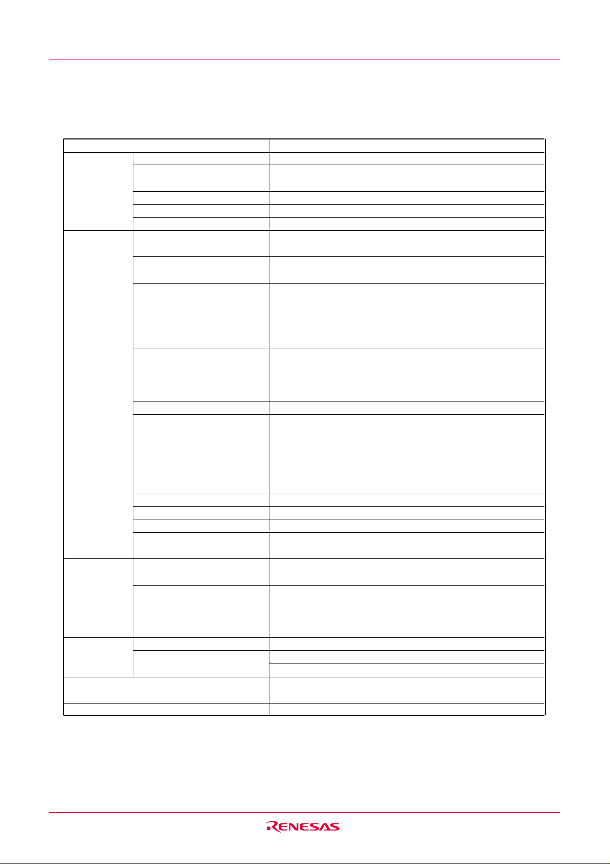
1.2 Performance Outline
Table 1.1. lists the performance outline of this MCU.
Table 1.1 Performance outline
Item Performance
CPU Number of basic instructions 89 instructions
Shortest instruction execution time
Operating mode Single-chip
Address space 1M bytes
Memory capacity See Table 1.2.
Peripheral Interrupt Internal: 11 factors, External: 5 factors,
function Software: 4 factors, Priority level: 7 levels
Watchdog timer 15 bits x 1 (with prescaler)
Timer Timer X: 8 bits x 1 channel, Timer Y: 8 bits x 1 channel,
Serial Interface •1 channel
A/D converter 10-bit A/D converter: 1 circuit, 12 channels
Clock generation circuit 2 circuits
Oscillation stop detection function
Voltage detection circuit Included
Power on reset circuit Included
Port Input/Output: 22 (including LED drive port), Input: 2
Electrical Power supply voltage VCC = 3.0 to 5.5 V (f(XIN) = 20 MHZ)
characteristics
Power consumption Typ. 9 mA (VCC = 5.0 V, (f(XIN) = 20 MHZ, High-speed mode)
Flash memory
Operating ambient temperature -20 to 85 °C
Package 32-pin plastic mold LQFP
Program/erase voltage VCC = 2.7 to 5.5 V
Number of program/erase 10,000 times (Data area)
50 ns (f(XIN) = 20 MHZ, VCC = 3.0 to 5.5 V)
100 ns (f(XIN) = 10 MHZ, VCC = 2.7 to 5.5 V)
Reset start function selectable
Timer Z: 8 bits x 1 channel
(Each timer equipped with 8-bit prescaler)
Timer C: 16 bits x 1 channel
Circuits of input capture and output compare.
Clock synchronous, UART
•1 channel
UART
•Main clock generation circuit (Equipped with a built-in
feedback resistor)
•On-chip oscillator (high speed, low speed)
On High-speed on-chip oscillator the frequency adjustment function is usable.
Stop detection of main clock oscillation
(LED drive I/O port: 8)
VCC = 2.7 to 5.5 V (f(XIN) = 10 MHZ)
Typ. 5 mA (VCC = 3.0 V, (f(XIN) = 10 MHZ, High-speed mode)
Typ. 35µA(VCC = 3.0 V, Wait mode, Peripheral clock stops)
Typ. 0.7µA(VCC = 3.0 V, Stop mode)
1,000 times (Program area)
-40 to 85 °C (D-version)
Rev.1.00 Sep 30, 2004 page 2 of 26
REJ03B0069-0100Z
Page 3
R8C/13 Group 1. Overview
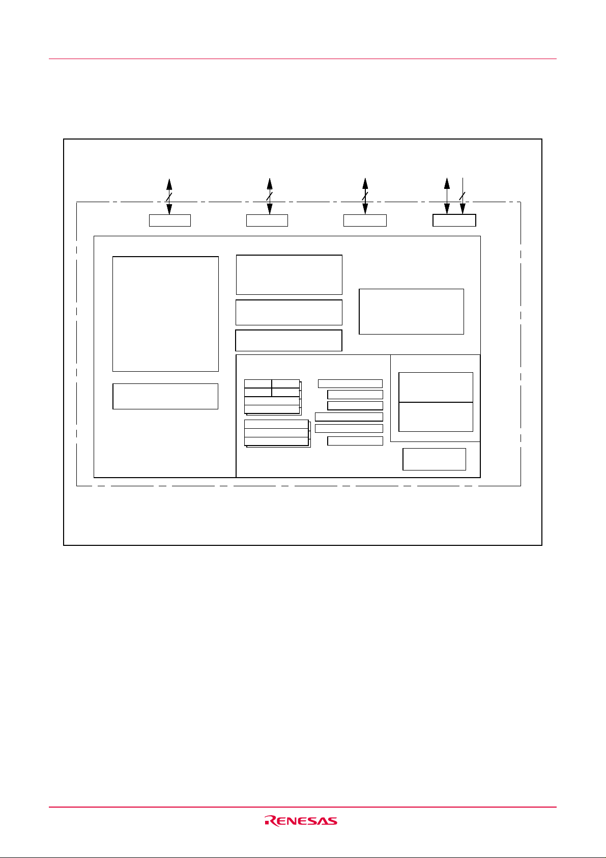
1.3 Block Diagram
Figure 1.1 shows this MCU block diagram.
I/O port
P o r t P 0
Pe r i p h e r a l f u n c t i o n s
T i m e r
Timer X (8 bits)
Timer Y (8 bits)
Timer Z (8 bits)
Timer C (16 bits)
Watchdog timer
(15 bits)
8
8
Port P1
A/D converter
(10 bits ✕ 12 channels)
UART or Clock synchronous
serial I/O
(8 bits ✕ 1 channel)
UART
(8 bits ✕ 1 channel)
R8C Series CPU c or e
R0LR 0 H
R 1 HR1L
R2
R3
A0
A1
FB
5
Port P3
System clock generator
X
High-speed on-chip oscillator
Low-speed on-chip oscillator
SB
USP
ISP
INTB
PC
FLG
IN-XOUT
M e m o r y
M u l t i p l i e r
1 2
P o r t P 4
R O M
( N o t e 1 )
RAM
(Note 2)
Figure 1.1 Block Diagram
N o t e 1 : R O M s i z e d e p e n d s o n M C U t y p e .
N o t e 2 : R A M s i z e d e p e n d s o n M C U t y p e .
Rev.1.00 Sep 30, 2004 page 3 of 26
REJ03B0069-0100Z
Page 4
R8C/13 Group 1. Overview
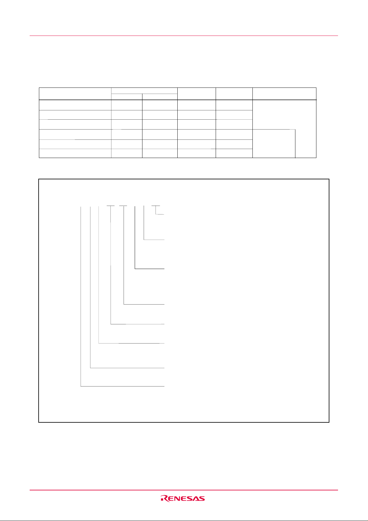
1.4 Product Information
Table 1.2 lists the products.
Table 1.2 Product List
Type No.
R5F21132FP
R5F21133FP
R5F21134FP
R5F21132DFP
R5F21133DFP
R5F21134DFP
ROM capacity
Program area
8K bytes
12K bytes
16K bytes
8K bytes
12K bytes
16K bytes
Type No. R 5 F 21 13 4 D FP
Data area
2K bytes x 2
2K bytes x 2
2K bytes x 2
2K bytes x 2
2K bytes x 2
2K bytes x 2
Package type:
FP : 32P6U
Shows characteristics and others.
D: Operating ambient temperature –40 °C to 85 °C
No symbol: Operating ambient temperature –20 °C to 85 °C
RAM capacity
512 bytes
768 bytes
1K bytes
512 bytes
768 bytes
1K bytes
Package type
32P6U-A
32P6U-A
32P6U-A
32P6U-A
32P6U-A
32P6U-A
As of September 2004
Remarks
Flash memory version
D version
ROM capacity:
2 : 8 KBytes.
3 : 12 KBytes.
4 : 16 KBytes.
R8C/13 group
R8C/Tiny series
Memory type:
F: Flash memory version
Renesas MCU
Renesas semiconductors
Figure 1.2 Type No., Memory Size, and Package
Rev.1.00 Sep 30, 2004 page 4 of 26
REJ03B0069-0100Z
Page 5
R8C/13 Group 1. Overview
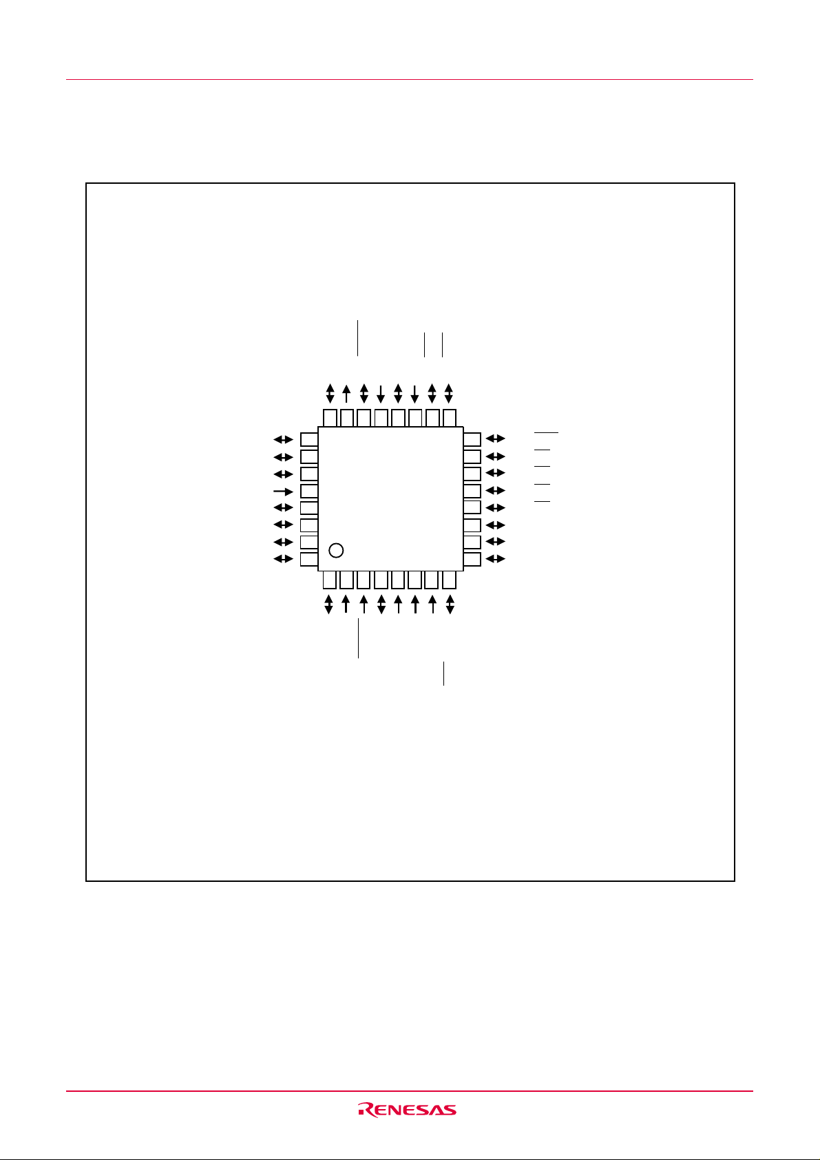
1.5 Pin Assignments
Figure 1.3 shows the pin configuration (top view).
PIN CONFIGURATION (top view)
2
1
0
1
P 06/ A N
P 05/ A N
P 04/ A N
M O D E
P 03/ A N
P 02/ A N
P 01/ A N
P00/AN7/TxD
1
/
0
R
0
N
3
S
/
/
C
S
0
7
C
3
0
A
P
V
V
C N T
C M P
P
I
U
T
A
C M P
2 4 2 3 2 2 2 1 2 0 1 9 1 8 1 7
2 5
1
2 6
2
2 7
3
2 8
2 9
4
3 0
5
3 1
6
11
3 2
R 8 C / 1 3 G r o u p
1 2 3 4 5 6 7 8
/
1
1
R
N
I
/
T
O
Z
/
1
3
E
P
C
F
T
/
/
3
2
R
T
T
V
/
C
/
/
C
3
2
3
3
V
I N
I N
C N T
P
P
C M P
A
1 6
1 5
1 4
1 3
1 2
1 1
1 0
P 45/ I N T
P 10/ K I0/ A N8/ C M P 0
P 11/ K I1/ A N9/ C M P 0
P 12/ K I2/ A N
P 13/ K I3/ A N
P 14/ T x D
P 15/ R x D
9
P16/CLK
0
0
1
1 0
/ C M P 0
2
1 1
0
0
0
1
D
/
0
1
D
N
/
7
3
P
R x
T x
N o t e s :
1 . P 4
7
f u n c t i o n s o n l y a s a n i n p u t p o r t .
2. W h e n u s i n g O n - c h i p d e b u g g e r , d o n o t u s e p i n s P 0
a n d P 37/ T x D
1 0
/ R x D1.
3 . D o n o t c o n n e c t I V c c t o V c c .
Figure 1.3 Pin Configuration (Top View)
)
6
S
S
V
C
E S E
S
T
S
V
P
R
7
4
/
T
O
X
(N o t e 1
U
P
0
C
4
C
R
V
/
N
I
X
/
1
T
/
7
1
P
I N
C N T
0
/ A N7/ T x D
1 1
Package: 32P6U-A
Rev.1.00 Sep 30, 2004 page 5 of 26
REJ03B0069-0100Z
Page 6
R8C/13 Group 1. Overview
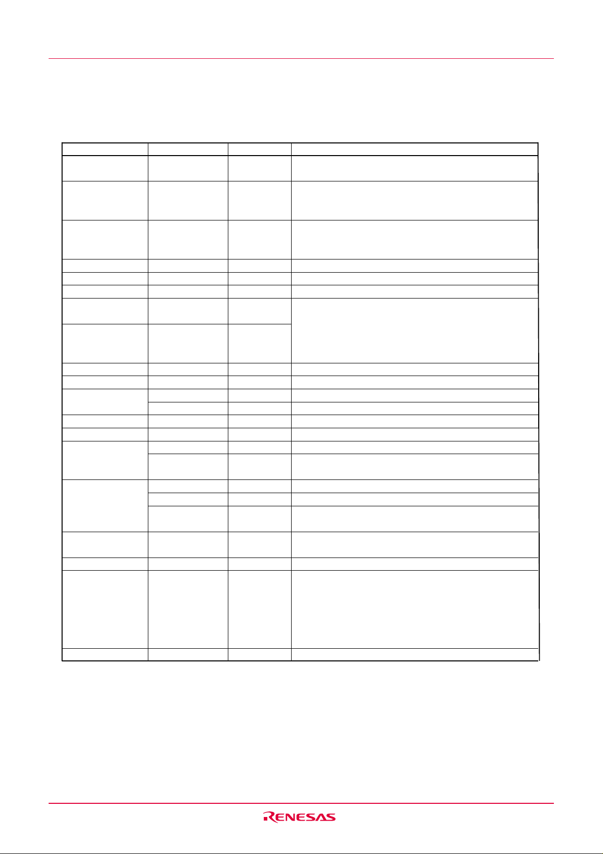
1.6 Pin Description
Table 1.3 shows the pin description
Table 1.3 Pin description
Signal name Pin name I/O type
Power supply Vcc, I
input Vss
IVcc IVcc O
Analog power AVcc, AVss I
supply input
Reset input
___________
RESET I
CNVss CNVss I
MODE MODE I
Main clock input XIN I
Main clock output XOUT O
_____
INT interrupt input
Key input interrupt
Timer X CNTR0 I/O
_______ _______
INT0 to INT3 I
_____ _____
KI0 to KI3 I
__________
CNTR0 O
Timer Y CNTR1 I/O
Timer Z TZOUT O
Timer C TCIN I
CMP00 to CMP03,
O
CMP10 to CMP13
Serial interface CLK0 I/O
RxD0, RxD1 I
TxD0, TxD10,O
TxD11
Reference voltage VREF I
input
A/D converter AN0 to AN11 I
I/O port P00 to P07, I/O
P10 to P17,
P30 to P33, P37,
P45
Input port P46, P47 I
Apply 2.7 V to 5.5 V to the Vcc pin. Apply 0 V to the
Vss pin.
This pin is to stabilize internal power supply.
Connect this pin to Vss via a capacitor (0.1 µF).
Do not connect to Vcc.
These are power supply input pins for A/D converter.
Connect the AVss pin to Vss. Connect a capacitor
between pins AVcc and AVss.
“L” on this input resets the MCU.
Connect this pin to Vss via a resistor.
Connect this pin to Vcc via a resistor.
These pins are provided for the main clock generating circuit I/O. Connect a ceramic resonator or a crystal oscillator between the XIN and XOUT pins. To use
an externally derived clock, input it to the XIN pin and
leave the XOUT pin open.
______
These are INT interrupt input pins.
These are key input interrupt pins.
This is the timer X I/O pin.
This is the timer X output pin.
This is the timer Y I/O pin.
This is the timer Z output pin.
This is the timer C input pin.
These are the timer C output pins.
This is a transfer clock I/O pin.
These are serial data input pins.
These are serial data output pins.
This is a reference voltage input pin for A/D converter.
These are analog input pins for A/D converter.
These are 8-bit CMOS I/O ports. Each port has an I/O
select direction register, allowing each pin in that port
to be directed for input or output individually.
Any port set to input can select whether to use a pullup resistor or not by program.
P10 to P17 also function as LED drive ports.
These are input only pins.
Function
Rev.1.00 Sep 30, 2004 page 6 of 26
REJ03B0069-0100Z
Page 7
R8C/13 Group 2. Central Processing Unit (CPU)
g
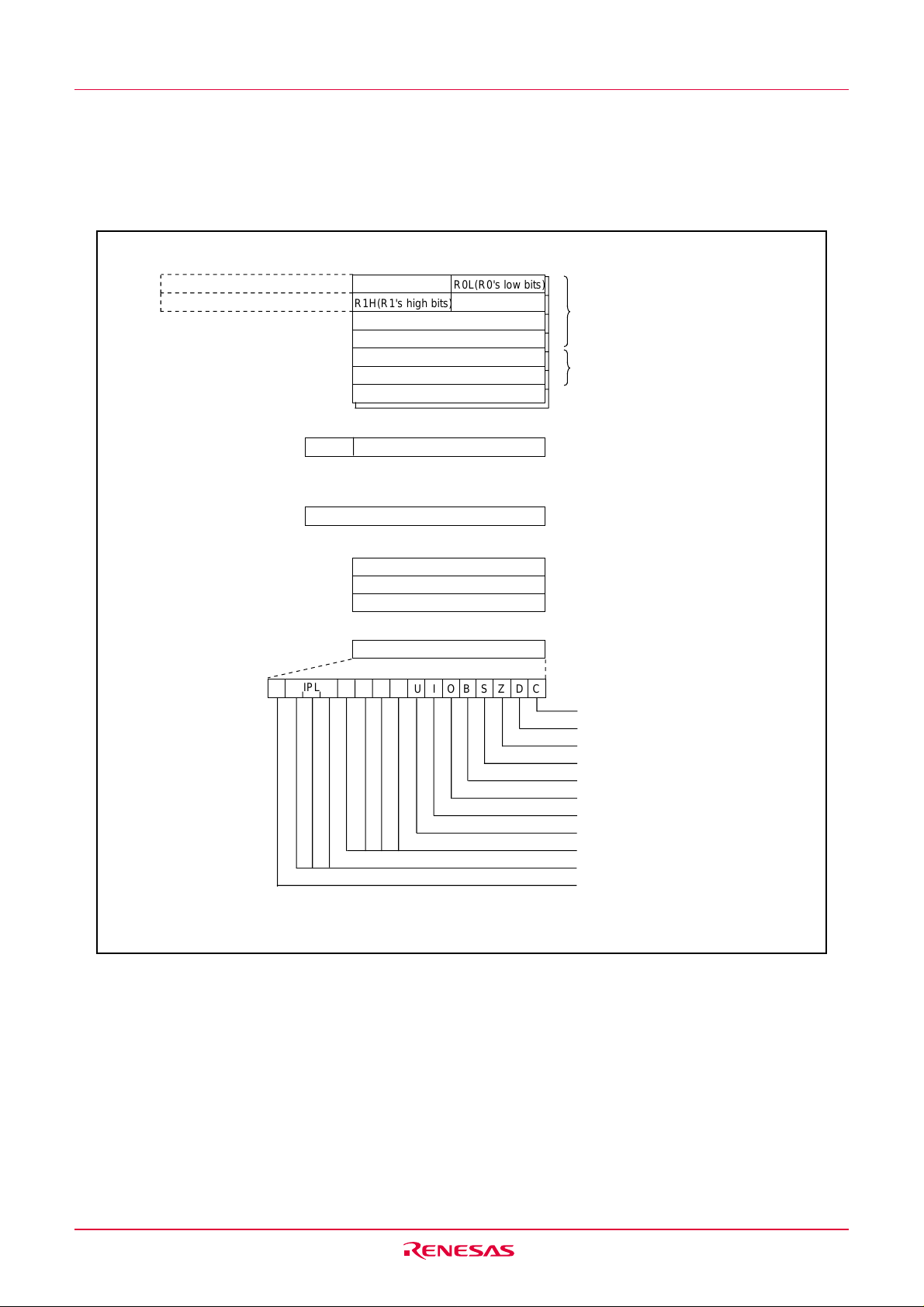
2. Central Processing Unit (CPU)
Figure 2.1 shows the CPU registers. The CPU has 13 registers. Of these, R0, R1, R2, R3, A0, A1 and FB
comprise a register bank. There are two register banks.
b31
R2
R3
b15
R0H(R0's high bits)
R1H(R1's high bits)
b19
b15
INTBH
The upper 4 bits of INTB are INTBH and
the lower 16 bits of INTB are INTBL.
b19
PC
b15
b15
b15
b7 b8
IPL
b8 b7 b0
R0L(R0's low bits)
R1L(R1's low bits)
R2
R3
A0
A1
FB
INTBL
USP
ISP
SB
FLG
Data registers (Note 1)
Address registers (Note 1)
Frame base registers (Note 1)
b0
Interrupt table register
b0
Program counter
b0
User stack pointer
Interrupt stack pointer
Static base register
b0
Flag register
b0
CDZSBOIU
Carry flag
Debug flag
Zero flag
Sign flag
Register bank select flag
Overflow flag
Interrupt enable flag
Stack pointer select flag
Reserved area
Processor interrupt priority level
Reserved area
Note 1: These re
isters comprise a register bank. There are two register banks.
Figure 2.1 Central Processing Unit Register
2.1 Data Registers (R0, R1, R2 and R3)
The R0 register consists of 16 bits, and is used mainly for transfers and arithmetic/logic operations. R1 to
R3 are the same as R0.
The R0 register can be separated between high (R0H) and low (R0L) for use as two 8-bit data registers.
R1H and R1L are the same as R0H and R0L. Conversely, R2 and R0 can be combined for use as a 32bit data register (R2R0). R3R1 is the same as R2R0.
Rev.1.00 Sep 30, 2004 page 7 of 26
REJ03B0069-0100Z
Page 8

R8C/13 Group 2. Central Processing Unit (CPU)
2.2 Address Registers (A0 and A1)
The register A0 consists of 16 bits, and is used for address register indirect addressing and address
register relative addressing. They also are used for transfers and logic/logic operations. A1 is the same as A0.
In some instructions, registers A1 and A0 can be combined for use as a 32-bit address register (A1A0).
2.3 Frame Base Register (FB)
FB is configured with 16 bits, and is used for FB relative addressing.
2.4 Interrupt Table Register (INTB)
INTB is configured with 20 bits, indicating the start address of an interrupt vector table.
2.5 Program Counter (PC)
PC is configured with 20 bits, indicating the address of an instruction to be executed.
2.6 User Stack Pointer (USP) and Interrupt Stack Pointer (ISP)
Stack pointer (SP) comes in two types: USP and ISP, each configured with 16 bits.
Your desired type of stack pointer (USP or ISP) can be selected by the U flag of FLG.
2.7 Static Base Register (SB)
SB is configured with 16 bits, and is used for SB relative addressing.
2.8 Flag Register (FLG)
FLG consists of 11 bits, indicating the CPU status.
2.8.1 Carry Flag (C Flag)
This flag retains a carry, borrow, or shift-out bit that has occurred in the arithmetic/logic unit.
2.8.2 Debug Flag (D Flag)
The D flag is used exclusively for debugging purpose. During normal use, it must be set to “0”.
2.8.3 Zero Flag (Z Flag)
This flag is set to “1” when an arithmetic operation resulted in 0; otherwise, it is “0”.
2.8.4 Sign Flag (S Flag)
This flag is set to “1” when an arithmetic operation resulted in a negative value; otherwise, it is “0”.
2.8.5 Register Bank Select Flag (B Flag)
Register bank 0 is selected when this flag is “0” ; register bank 1 is selected when this flag is “1”.
2.8.6 Overflow Flag (O Flag)
This flag is set to “1” when the operation resulted in an overflow; otherwise, it is “0”.
2.8.7 Interrupt Enable Flag (I Flag)
This flag enables a maskable interrupt.
Maskable interrupts are disabled when the I flag is “0”, and are enabled when the I flag is “1”. The I
flag is cleared to “0” when the interrupt request is accepted.
2.8.8 Stack Pointer Select Flag (U Flag)
ISP is selected when the U flag is “0”; USP is selected when the U flag is “1”.
The U flag is cleared to “0” when a hardware interrupt request is accepted or an INT instruction for
software interrupt Nos. 0 to 31 is executed.
2.8.9 Processor Interrupt Priority Level (IPL)
IPL is configured with three bits, for specification of up to eight processor interrupt priority levels from
level 0 to level 7.
If a requested interrupt has priority greater than IPL, the interrupt is enabled.
2.8.10 Reserved Area
When write to this bit, write "0". When read, its content is indeterminate.
Rev.1.00 Sep 30, 2004 page 8 of 26
REJ03B0069-0100Z
Page 9
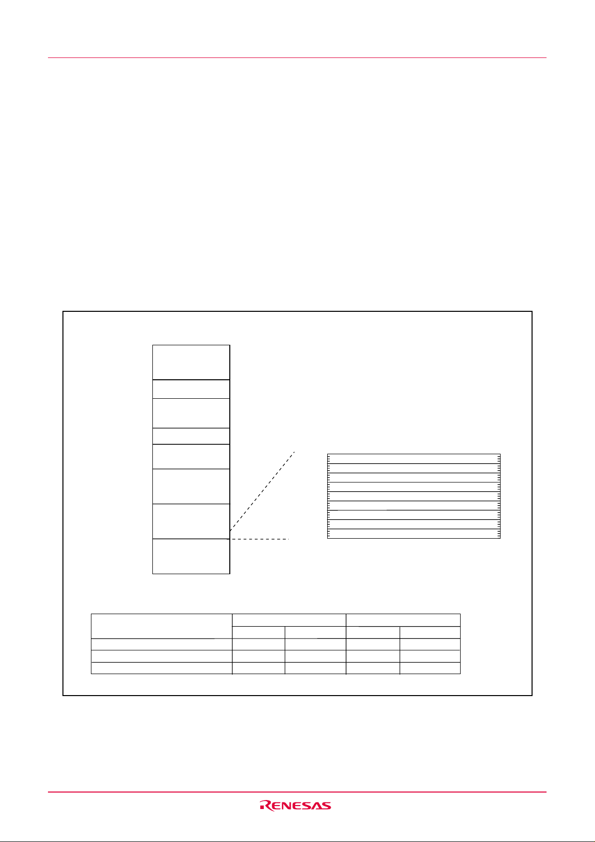
R8C/13 Group 3. Memory
3. Memory
Figure 3.1 is a memory map of this MCU. The address space extends the 1M bytes from address 0000016
to FFFFF16.
The internal ROM (program area) is allocated in a lower address direction beginning with address 0FFFF16.
For example, a 16-Kbyte internal ROM is allocated to the addresses from 0C00016 to 0FFFF16.
The fixed interrupt vector table is allocated to the addresses from 0FFDC
the start address of each interrupt routine here.
The internal ROM (data area) is allocated to the addresses from 0200016 to 02FFF16.
The internal RAM is allocated in an upper address direction beginning with address 0040016. For example,
a 1-Kbyte internal RAM is allocated to the addresses from 0040016 to 007FF16. In addition to storing data,
the internal RAM also stores the stack used when calling subroutines and when interrupts are generated.
Special function registers (SFR) are allocated to the addresses from 0000016 to 002FF16. Peripheral function control registers are located here. Of the SFR, any space which has no functions allocated is reserved
for future use and cannot be used by users.
16 to 0FFFF16. Therefore, store
00000
002FF
00400
0XXXX
02000
02FFF
0YYYY
0FFFF
FFFFF
16
16
16
16
16
16
16
16
16
SFR
(See Chapter 4 for details.)
Internal RAM
Internal ROM
(data area)
Internal ROM
(program area)
Expanding area
1
0FFDC
0FFFF
16
Watchdog timer,Oscillation stop detection,Voltage detection
16
Undefined instruction
NOTES:
1. The data flash ROM block A (2K bytes) and block B (2K bytes) are shown.
2. Blank spaces are reserved. No access is allowed.
Type name
R5F21134FP, R5F21134DFP
R5F21133FP, R5F21133DFP
R5F21132FP, R5F21132DFP
Internal ROM
Size
16K bytes
12K bytes
8K bytes
Address 0YYYY
0C000
16
16
0D000
0E000
16
16
Internal RAM
Size
1K bytes
768 bytes
512 bytes
Overflow
BRK instruction
Address match
Single step
(Reserved)
(Reserved)
Reset
Address 0XXXX
007FF
006FF
005FF
16
16
16
16
Figure 3.1 Memory Map
Rev.1.00 Sep 30, 2004 page 9 of 26
REJ03B0069-0100Z
Page 10

R8C/13 Group 4. Special Function Register (SFR)
4. Special Function Register (SFR)
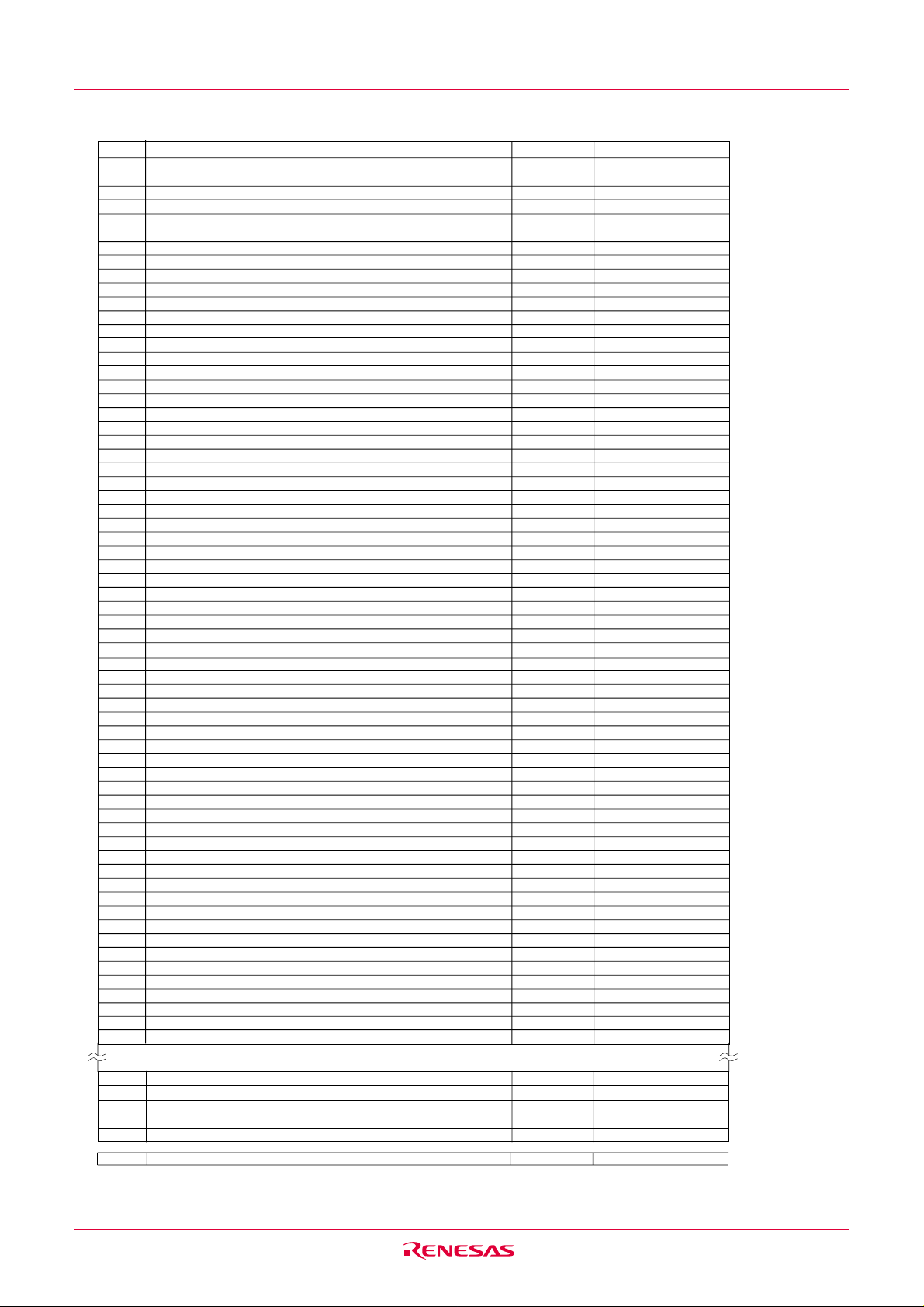
SFR(Special Function Register) is the control register of peripheral functions. Tables 4.1 to 4.4 list the SFR
information
Table 4.1 SFR Information(1)
Address
000016
000116
000216
000316
Processor mode register 0 PM0 00
000416
000516
Processor mode register 1 PM1 00
000616
System clock control register 0 CM0 01101000
000716
System clock control register 1 CM1 00100000
000816
High-speed on-chip oscillator control register 0 HR0 00
000916
Address match interrupt enable register AIER XXXXXX00
000A16
Protect register PRCR 00XXX000
000B16
High-speed on-chip oscillator control register 1 HR1 40
000C16
Oscillation stop detection register OCD 00000100
000D16
Watchdog timer reset register WDTR XX
000E16
Watchdog timer start register WDTS XX
000F16
Watchdog timer control register WDC 000XXXXX
001016
Address match interrupt register 0 RMAD0 00
001116
001216
001316
001416
Address match interrupt register 1 RMAD1 00
001516
001616
001716
001816
001916
Voltage detection register 1 VCR1 00
001A16
Voltage detection register 2 VCR2 10000000
001B16
001C16
001D16
001E16
INT0 input filter select register INT0F XXXXX000
001F16
Voltage detection interrupt register D4INT 00
002016
002116
002216
002316
002416
002516
002616
002716
002816
002916
002A16
002B16
002C16
002D16
002E16
002F16
003016
003116
003216
003316
003416
003516
003616
003716
003816
003916
003A16
003B16
003C16
003D16
003E16
003F16
X : Undefined
NOTES:
1. Blank columns are all reserved space. No access is allowed.
2. Software reset or the watchdog timer reset does not affect this register.
3. Owing to Reset input.
4. In the case of
RESET
pin = H retaining.
(1)
Register Symbol After reset
1
2
2
2
00
X0
00
X0
16
16
16
16
16
16
16
16
16
16
16
16
16
16
2
2
2
2
2
2
16
2
3
01000001
4
2
Rev.1.00 Sep 30, 2004 page 10 of 26
REJ03B0069-0100Z
Page 11

R8C/13 Group 4. Special Function Register (SFR)
Table 4.2 SFR Information(2)
Address
0040
16
0041
16
0042
16
0043
16
0044
16
0045
16
0046
16
0047
16
0048
16
0049
16
004A
16
004B
16
004C
16
004D
16
Key input interrupt control register KUPIC XXXXX000
004E
16
A/D conversion interrupt control register ADIC XXXXX000
004F
16
0050
16
Compare 1 interrupt control register
0051
16
UART0 transmit interrupt control register
0052
16
UART0 receive interrupt control register
0053
16
UART1 transmit interrupt control register
0054
16
UART1 receive interrupt control register
0055
16
INT2 interrupt control register INT2IC XXXXX000
0056
16
Timer X interrupt control register TXIC XXXXX000
0057
16
Timer Y interrupt control register TYIC XXXXX000
0058
16
Timer Z interrupt control register TZIC XXXXX000
0059
16
INT1 interrupt control register INT1IC XXXXX000
005A
16
INT3 interrupt control register INT3IC XXXXX000
005B
16
Timer C interrupt control register TCIC XXXXX000
005C
16
Compare 0 interrupt control register
005D
16
INT0 interrupt control register INT0IC XX00X000
005E
16
005F
16
0060
16
0061
16
0062
16
0063
16
0064
16
0065
16
0066
16
0067
16
0068
16
0069
16
006A
16
006B
16
006C
16
006D
16
006E
16
006F
16
0070
16
0071
16
0072
16
0073
16
0074
16
0075
16
0076
16
0077
16
0078
16
0079
16
007A
16
007B
16
007C
16
007D
16
007E
16
007F
16
(1)
Register Symbol After reset
X : Undefined
NOTES:
1. Blank columns are all reserved space. No access is allowed.
CMP1IC XXXXX000
S0TIC XXXXX000
S0RIC XXXXX000
S1TIC XXXXX000
S1RIC XXXXX000
CMP0IC XXXXX000
2
2
2
2
2
2
2
2
2
2
2
2
2
2
2
2
Rev.1.00 Sep 30, 2004 page 11 of 26
REJ03B0069-0100Z
Page 12

R8C/13 Group 4. Special Function Register (SFR)
Table 4.3 SFR Information(3)
Address
0080
16
Timer Y, Z mode register TYZMR 00
0081
16
Prescaler Y PREY FF
0082
16
Timer Y secondary TYSC FF
Timer Y primary TYPR FF
0083
16
0084
16
Timer Y, Z waveform output control register PUM 00
0085
16
Prescaler Z PREZ FF
0086
16
Timer Z secondary TZSC FF
0087
16
Timer Z primary TZPR FF
0088
16
0089
16
Timer Y, Z output control register TYZOC 00
008A
16
Timer X mode register TXMR 00
008B
16
008C
16
Prescaler X PREX FF
Timer X register TX FF
008D
16
Timer count source setting register TCSS 00
008E
16
008F
16
0090
16
Timer C register TC 00
0091
16
0092
16
0093
16
0094
16
0095
16
0096
16
External input enable register INTEN 00
0097
16
Key input enable register KIEN 00
0098
16
0099
16
009A
16
Timer C control register 0 TCC0 00
009B
16
Timer C control register 1 TCC1 00
009C
16
Capture, compare 0 register TM0 FF
009D
16
009E
16
Compare 1 register TM1 FF
009F
16
00A0
16
UART0 transmit/receive mode register
00A1
16
UART0 bit rate generator U0BRG XX
00A2
16
UART0 transmit buffer register U0TB XX
00A3
16
00A4
16
UART0 transmit/receive control register 0
00A5
16
UART0 transmit/receive control register 1
00A6
16
UART0 receive buffer register U0RB XX
00A7
16
00A8
16
UART1 transmit/receive mode register
00A9
16
UART1 bit rate register U1BRG XX
00AA
16
UART1 transmit buffer register U1TB XX
00AB
16
00AC
16
UART1 transmit/receive control register 0
00AD
16
UART1 transmit/receive control register 1
00AE
16
UART1 receive buffer register U1RB XX
00AF
16
00B0
16
UART transmit/receive control register 2
00B1
16
00B2
16
00B3
16
00B4
16
00B5
16
00B6
16
00B7
16
00B8
16
00B9
16
00BA
16
00BB
16
00BC
16
00BD
16
00BE
16
00BF
16
(1)
Register Symbol After reset
X : Undefined
NOTES:
1. Blank columns are all reserved space. No access is allowed.
16
16
16
16
16
16
16
16
16
16
16
16
16
16
00
16
16
16
16
16
16
FF
16
16
FF
U0MR 00
16
16
16
16
XX
16
U0C0 00001000
U0C1 00000010
16
XX
U1MR 00
16
16
16
16
XX
16
U1C0 00001000
U1C1 00000010
16
XX
UCON 00
16
16
2
2
2
2
Rev.1.00 Sep 30, 2004 page 12 of 26
REJ03B0069-0100Z
Page 13
R8C/13 Group 4. Special Function Register (SFR)
Table 4.4 SFR Information(4)
Address
00C0
16
A/D register AD XX
00C1
16
00C2
16
00C3
16
00C4
16
00C5
16
00C6
16
00C7
16
00C8
16
00C9
16
00CA
16
00CB
16
00CC
16
00CD
16
00CE
16
00CF
16
00D0
16
00D1
16
00D2
16
00D3
16
00D4
16
A/D control register 2 ADCON2 00
00D5
16
00D6
16
A/D control register 0 ADCON0 00000XXX
00D7
16
A/D control register 1 ADCON1 00
00D8
16
00D9
16
00DA
16
00DB
16
00DC
16
00DD
16
00DE
16
00DF
16
00E0
16
Port P0 register P0 XX
00E1
16
Port P1 register P1 XX
00E2
16
Port P0 direction register PD0 00
00E3
16
Port P1 direction register PD1 00
00E4
16
00E5
16
Port P3 register P3 XX
00E6
16
00E7
16
Port P3 direction register PD3 00
00E8
16
Port P4 register P4 XX
00E9
16
Port P4 direction register PD4 00
00EA
16
00EB
16
00EC
16
00ED
16
00EE
16
00EF
16
00F0
16
00F1
16
00F2
16
00F3
16
00F4
16
00F5
16
00F6
16
00F7
16
00F8
16
00F9
16
03FA
16
00FB
16
Pull-up control register 0 PUR0 00XX0000
00FC
16
00FD
16
Pull-up control register 1 PUR1 XXXXXX0X
00FE
16
Port P1 drive capacity control register DRR 00
Timer C output control register TCOUT 00
00FF
16
(1)
Register
Symbol After reset
16
XX
16
16
2
16
16
16
16
16
16
16
16
16
2
16
16
2
Flash memory control register 4 FMR4 01000000
01B3
16
01B4
16
01B5
16
Flash memory control register 1 FMR1 1000000X
01B6
16
01B7
16
Flash memory control register 0 FMR0 00000001
0FFFF
16
Option function select register
X : Undefined
NOTES:
1. The blank areas, 0100
2. The watchdog timer control bit is assigned. Refer to "Figure11.2 OFS, WDC, WDTR and WDTS registers" for the OFS register details
16
to 01B216 and 01B816 to 02FF16 are reserved and cannot be used by users.
(2)
OFS
Note 2
2
2
2
Rev.1.00 Sep 30, 2004 page 13 of 26
REJ03B0069-0100Z
Page 14

R8C/13 Group 5. Electrical Characteristics
5. Electrical Characteristics
Table 5.1 Absolute Maximum Ratings
Symbol
V
CC
AV
CC
V
I
O
V
P
d
T
opr
T
stg
Parameter Unit
Supply voltage
Analog supply voltage
Input voltage
Output voltage
Power dissipation
Operating ambient temperature
Storage temperature
Condition
VCC=AV
CC
V
CC
=AV
CC
C
Topr=25
Rated value
-0.3 to 6.5
-0.3 to 6.5
CC
-0.3 to V
-0.3 to VCC+0.3
-20 to 85 / -40 to 85 (D version)
+0.3
300
-65 to 150
V
V
V
V
mW
C
C
Table 5.2
Symbol
V
CC
AVcc
Vss
AVss
IH
V
V
IL
I
OH (sum)
I
OH (peak)
I
OH (avg)
I
OL (sum)
I
OL (peak)
I
OL (avg)
f (XIN)
Recommended Operating Conditions
Parameter
Supply voltage
Analog supply voltage
Supply voltage
Analog supply voltage
"H" input voltage
"L" input voltage
"H" peak all
output currents
"H" peak output current
"H" average output current
"L" peak all
output currents
"L" peak output
current
"L" average
output current
Main clock input oscillation frequency
Sum of all pins' IOH
(peak)
Sum of all pins' IOL
(peak)
Except P1
P10 to P1
Except P1
P10 to P1
0
to P1
7
0
to P1
7
7
Drive ability HIGH
Drive ability LOW
7
Drive ability HIGH
Drive ability LOW
3.0V ≤ Vcc ≤ 5.5V
2.7V ≤ Vcc < 3.0V
Note
1: Referenced to V
CC
= AVCC = 2.7 to 5.5V at Topr = -20 to 85 °C / -40 to 85 °C unless otherwise specified.
2: The mean output current is the mean value within 100ms.
3: Set Vcc=AVcc
Conditions
Min.
0.8V
2.7
Standard
Typ.
3
V
CC
0
0
CC
0
0
0
Max.
5.5
CC
V
0.2V
-60.0
-10.0
-5.0
60
10
30
10
5
15
5
20
10
Unit
V
V
V
V
V
CC
V
mA
mA
mA
mA
mA
mA
mA
mA
mA
mA
MHz
MHz
Rev.1.00 Sep 30, 2004 page 14 of 26
REJ03B0069-0100Z
Page 15

R8C/13 Group 5. Electrical Characteristics
Table 5.3 A/D Conversion Characteristics
Symbol Parameter Measuring condition
ref
=V
CC
V
f(XIN)=øAD=10 MHz, Vref=Vcc=5.0V
f(XIN)=øAD=10 MHz, Vref=Vcc=5.0V
f(XIN)=øAD=10 MHz, Vref=Vcc=3.3V
f(XIN)=øAD=10 MHz, Vref=Vcc=3.3V
V
REF=VCC
f(XIN)=øAD=10 MHz, Vref=Vcc=5.0V
f(XIN)=øAD=10 MHz, Vref=Vcc=5.0V
R
LADDER
tCONV
VREF
V
IA
Resolution
–
Absolute
–
accuracy
Ladder resistance
Conversion time
Reference voltage
Analog input voltage
A/D operation
–
clock frequency
10 bit mode
8 bit mode
10 bit mode
8 bit mode
10 bit mode
8 bit mode
Without sample & hold
2
With sample & hold
Standard
Min. Typ. Max.
10
3.3
2.8
0
0.25
1.0
Note
1: Referenced to V
2: When f
AD
CC
=AVCC=2.7 to 5.5V at Topr = -20 to 85 °C / -40 to 85 °C unless otherwise specified.
is 10 MHz more, divide the f
AD
and make A/D operation clock frequency (Ø
AD)
lower than
10 MHz.
3: When the Vcc is less than 4.2V, divide the f
AD
and make A/D operation clock frequency (Ø
AD)
lower than fAD/2.
4: Set Vcc=Vref
VCC
10
±2
±5 LSB
±2
40
4
V
10
10
Unit
Bit
LSB±3
LSB
LSB
kΩ
µs
µs
V
ref
V
MHz
MHz
P0
P1
P2
P3
P4
Figure 5.1 Port P0 to P4 measurement circuit
30pF
Rev.1.00 Sep 30, 2004 page 15 of 26
REJ03B0069-0100Z
Page 16

R8C/13 Group 5. Electrical Characteristics
–
–
–
–
–
–––
–
Table 5.4
Symbol
d(SR-ES)
t
Table 5.5
S y m b o l
d(SR-ES)
t
Note
1: Referenced to V
2: Definition of Program/Erase
The cycle of Program/Erase shows a cycle for each block.
If the program/erase number is “n” (n = 1000, 10000), “n” times erase can be performed for each block.
For example, if performing one-byte write to the distinct addresses on Block A of 2K-byte block 2048 times and then
erasing that block, the number of Program/Erase cycles is one time.
However, performing multiple writes to the same address before an erase operation is prohibited (overwriting
prohibited).
3: Maximum numbers of Program/Erase cycles for which all electrical characteristics is guaranteed.
4: Table 16.5 applies for Block A or B when the Program/Erase cycles are more than 1000. The byte program time up to
1000 cycles are the same as that of the program area (see Table 5.4).
5: To reduce the number of Program/Erase cycles, a block erase should ideally be performed after writing in series as
many distinct addresses (only one time each) as possible. If programming a set o f 16 bytes, write up to 128 sets and
then erase them one time. This will result in ideally reducing the number of Program/Erase cycles. Additionally,
averaging the number of Program/Erase cycles for Block A and B will be more effective. It is important to track the total
number of block erases and restrict the number.
6: If error occurs during block erase, attempt to execute the clear status register command, then the block erase
command at least three times until the erase error disappears.
7: Customers desiring Program/Erase failure rate information should contact their Renesas technical support representa-
tive.
8: -40 °C for D version.
Flash Memory (Program area) Electrical Characteristics
Parameter
Program/Erase cycle
–
Byte program time
–
–
Block erase time
Time delay from Suspend Request until Erase Suspend
Program, Erase Voltage
–
Read Voltage
–
–
–
Program, Erase Temperature
Data-retention duration
2
Measuring condition
V
CC
= 5.0 V at Topr = 25 °C
V
CC
= 5.0 V at Topr = 25 °C
Topr = 55 °C
Flash Memory (Data area Block A, Block B) Electrical Characteristics
P a r a m e t e r
Pr o g r a m / E r a s e e n d u r a n c e
B y t e p r o g r a m t i m e ( p r o g r a m / e r a s e e n d u r a n c e
≤1 0 0 0 t i m e s )
B y t e p r o g r a m t i m e ( p r o g r a m / e r a s e e n d u r a n c e
>1 0 0 0 t i m e s )
B l o c k e r a s e t i m e ( p r o g r a m / e r a s e e n d u r a n c e
≤1 0 0 0 t i m e s )
B l o c k e r a s e t i m e ( p r o g r a m / e r a s e e n d u r a n c e
> 1 0 0 0 t i m e s )
Time delay from Suspend Request
until Erase Suspend
Program, Erase Voltage
Read Voltage
Program/Erase Temperature
D a t a - r e t e n t i o n d u r a t i o n
CC=AVcc=2.7 to 5.5V at Topr = 0°C to 60°C unless otherwise specified.
2
Measuring condition
5 . 0 V a t T o p r = 2 5 °
C
VC
=
5 . 0 V a t T o p r = 2 5 °
C
VC
=
VCC = 5.0 V at Topr = 25 °C
CC = 5.0 V at Topr = 25 °C
V
Topr = 55 °C
Standard
Min. Typ. Max
3
1000
50
0.4
2.7
2.7
0
20
4
Standard
Min. Typ. Max
3
10 0 0 0
C
C
2.7
2.7
-20(-40)
20
5 0
6 5
0.2
0 . 3
8
8
5.5
5.5
60
400
9
8
5.5
5.5
85
Unit
cycle
µs
s
ms
V
V
°C
year
U n i t
t i m e s
µs
µ s
s
s
m s
V
V
° C
year
Erase-suspend request
(interrupt request)
FMR46
t
d(SR-ES)
Figure 5.2 Time delay from Suspend Request until Erase Suspend
Rev.1.00 Sep 30, 2004 page 16 of 26
REJ03B0069-0100Z
Page 17

R8C/13 Group 5. Electrical Characteristics
Table 5.6
Symbol
Vdet
td(E-A)
Vccmin
Voltage Detection Circuit Electrical Characteristics
Parameter
Voltage detection level
Voltage detection interrupt request generating time
Voltage detection circuit self consumption current
Waiting time until voltage detection circuit operation starts
Microcomputer operation voltage minimum value
2
3
Measuring condition
VC27=1, VCC=5.0V
Standard
Typ.
Min. Max.
3.3
600
2.7
4.3
40
20
NOTES:
1. The measuring condition is Vcc=AVcc=2.7V to 5.5V and Topr=-40°C to 85°C.
2. This shows the time until the voltage detection interrupt request is generated since the voltage passes Vdet.
3. This shows the required time until the voltage detection circuit operates when setting to "1" again after setting the VC27 bit in the VCR2
“
”
Table 5.7
Symbol
Vpor2
t
w(Vpor2-
Vdet)
t
w(por2)
Reset Circuit Electrical Characteristics (When Using Hardware Reset 2)
Parameter
Power-on reset valid voltage
Supply voltage rising time when power-on reset is canceled
Time to hold external power below valid voltage
2
Measuring condition
Standard
Typ.
Min. Max.
0
Vdet
100
NOTES:
1. The voltage detection circuit which is embedded in a microcomputer is a factor to generate the hardware reset 2. Refer to 5.1.2 Hardware
Reset 2 of Hardware Manual for details.
2. This condition is not applicable when using with Vcc ≥ 1.0V.
3. When turning power on after the time to hold the external power below effective voltage exceeds 10s, refer to Table 5.8 Reset Circuit
Electrical Characteristics (When Not Using Voltage Moitor 1 Reset).
Table 5.8
Symbol
Vpor1
t
w(Vpor1-
Vdet)
t
w(por1)
t
w(Vpor1-
Vdet)
t
w(por1)
t
w(Vpor1-
Vdet)
t
w(por1)
t
w(Vpor1-
Vdet)
t
w(por1)
Reset Circuit Electrical Characteristics (When Not Using Hardware Reset 2)
Parameter
Power-on reset valid voltage
Supply voltage rising time when power-on reset is canceled
Time to hold external power on below valid voltage
Supply voltage rising time when power-on reset is canceled
Time to hold external power on below valid voltage
Supply voltage rising time when power-on reset is canceled
Time to hold external power on below valid voltage
Supply voltage rising time when power-on reset is canceled
Time to hold external power on below valid voltage
Measuring condition
0°C ≤ Topr ≤ 85°C
0°C ≤ Topr ≤ 85°C
-20°C ≤ Topr ≤ 0°C
-20°C ≤ Topr ≤ 0°C
-20°C ≤ Topr ≤ 0°C
-20°C ≤ Topr ≤ 0°C
0°C ≤ Topr ≤ 85°C
0°C ≤ Topr ≤ 85°C
Min. Max.
10
30
10
Standard
Typ.
0.1
100
100
1
0.5
1
NOTES:
1. When not the sing hardware reset 2, use with Vcc ≥ 2.7V.
Unit
V3.8
µs
nA
µs
V
Unit
V
ms
s
Unit
V
ms
s
ms
s
ms
s
ms
s
3
V
det
V
por1
t
w(por1)
Internal reset signal
(“L” effective)
NOTES:
1. Hold the voltage of the microcomputer operation voltage range (Vccmin or above) within sampling time.
2. A sampling clock is selectable. Refer to “5.4 Voltage Detection Circuit” of Hardware Manual for details.
3. V
det
shows the voltage detection level of the voltage detection circuit. Refer to “5.4 Voltage Detection Circuit”
of Hardware Manual for details.
Figure 5.3 Reset Circuit Electrical Characteristics
Rev.1.00 Sep 30, 2004 page 17 of 26
REJ03B0069-0100Z
t
w(Vpor1–Vdet)
f
1
RING-S
Sampling time
X 32
1,2
t
w(por2)tw(Vpor2 –Vdet)
V
cc min
V
por2
f
RING-S
3
V
det
1
X 32
Page 18

R8C/13 Group 5. Electrical Characteristics
Table 5.9
Symbol
td(HRoffset)
td(HR)
High-speed On-Chip Oscillator Circuit Electrical Characteristics
Parameter
High-speed on-chip oscillator frequency 1 / {td(HRoffset)+td(HR)} when the
reset is released
Settable high-speed on-chip oscillator minimum period
High-speed on-chip oscillator period adjusted unit
High-speed on-chip oscillator temperature dependence(1)
High-speed on-chip oscillator temperature dependence(2)
Measuring condition
VCC=5.0V, Topr=25 °C
16
" in the HR1 register
Set "40
VCC=5.0V, Topr=25 °C
Set "00
16
" in the HR1 register
Differences when setting "01
in the HR register
Frequency fluctuation in temperature range
of -10 °C to 50 °C
Frequency fluctuation in temperature range
of -40 °C to 85 °C
16
" and "0016"
NOTES:
1. The measuring condition is Vcc=AVcc=5.0 V and Topr=25 °C.
Table 5.10
Symbol
td(P-R)
td(R-S)
Power Circuit Timing Characteristics
Parameter
Time for internal power supply stabilization during powering-on
STOP release time
3
Measuring condition
2
Note
1: The measuring condition is Vcc=AVcc=2.7 to 5.5 V and Topr=25 °C.
2: This shows the wait time until the internal power supply generating circuit is stabilized during power-on.
3: This shows the time until BCLK starts from the interrupt acknowledgement to cancel stop mode.
Table 5.11
Symbol
V
OH
V
OL
T+-VT-
V
IH
I
I
IL
PULLUP
R
fXIN
R
f
RING-S
V
RAM
Electrical Characteristics
Parameter
"H" output voltage
"L" output voltage
Hysteresis
"H" input current
"L" input current
Pull-up resistance
Feedback resistance
Low-speed on-chip oscillator frequency
RAM retention voltage
(1) [Vcc=5V]
Except X
OUT
X
OUT
P10 to P1
7
Except X
OUT
P10 to P1
7
X
OUT
INT0, INT1, INT2, INT3, KI0, KI1,
2
, KI3, CNTRo, CNTR1, TCIN,
KI
0
, RxD
1
RxD
RESET
IN
X
Measuring condition
IOH=-5mA
IOH=-200µA
Drive capacity HIGH
Drive capacity LOW
IOH= 5 mA
I
OH
= 200 µA
Drive capacity HIGH
Drive capacity LOW
Drive capacity LOW
Drive capacity HIGH
Drive capacity LOW
V
I
=5V
V
I
=0V
I
=0V
V
At stop mode 2.0
IOH=-1 mA V
IOH=-500µA
OL
= 15 mA
I
I
OL
= 5 mA
I
OL
= 200 µA
IOL= 1 mA
I
OL
=500 µA
Note
1 : Referenced to V
CC
=AVCC=4.2 to 5.5V at Topr = -20 to 85 °C / -40 to 85 °C, f(BCLK)=20MHz unless otherwise specified.
Standard
Typ.
Min. Max.
6
8
61
1
±5
±10
Standard
Typ.
Min. Max.
Standard
Typ.
1.0
125
Max.
-5.0
50
V
V
V
Min.
CC
CC
CC
CC
0.2
0.2
-
2.0
-
0.3
-
2.0
-
2.0
30
40
150
V
V
V
V
2.0
0.45
2.0
2.0
0.45
2.0
2.0
1.0
167
250
10
2.2
5.0
Unit
MHz
ns
ns
%
%
Unit
ms
2
µs
Unit
V
CC
V
CC
V
CC
CC
V
V
V
V
V
V
V
V
V
V
µA
µA
kΩ
MΩ
kHz
V
Rev.1.00 Sep 30, 2004 page 18 of 26
REJ03B0069-0100Z
Page 19

R8C/13 Group 5. Electrical Characteristics
Table 5.12 Electrical Characteristics (2)
Symbol
Power supply current
I
CC
(VCC=3.3 to 5.5V)
In single-chip mode, the output
pins are open and other pins
are V
SS
Parameter
[Vcc=5V]
High-speed
mode
Medium-speed
mode
High-speed
on-chip oscillator
mode
Low-speed
on-chip oscillator
mode
Wait mode
Wait mode
Stop mode
Measuring condition
XIN=20 MHz (square wave)
High-speed on-chip oscillator off
Low-speed on-chip oscillator on=125 kHz
No division
XIN=16 MHz (square wave)
High-speed on-chip oscillator off
Low-speed on-chip oscillator on=125 kHz
No division
XIN=10 MHz (square wave)
High-speed on-chip oscillator off
Low-speed on-chip oscillator on=125 kHz
No division
XIN=20 MHz (square wave)
High-speed on-chip oscillator off
Low-speed on-chip oscillator on=125 kHz
Division by 8
XIN=16 MHz (square wave)
High-speed on-chip oscillator off
Low-speed on-chip oscillator on=125 kHz
Division by 8
XIN=10 MHz (square wave)
High-speed on-chip oscillator off
Low-speed on-chip oscillator on=125 kHz
Division by 8
Main clock off
High-speed on-chip oscillator on=8 MHz
Low-speed on-chip oscillator on=125 kHz
No division
Main clock off
High-speed on-chip oscillator on=8 MHz
Low-speed on-chip oscillator on=125 kHz
Division by 8
Main clock off
High-speed on-chip oscillator off
Low-speed on-chip oscillator on=125 kHz
Division by 8
Main clock off
High-speed on-chip oscillator off
Low-speed on-chip oscillator on=125 kHz
When a WAIT instruction is executed
Peripheral clock operation
VC27="0"
Main clock off
High-speed on-chip oscillator off
Low-speed on-chip oscillator on=125 kHz
When a WAIT instruction is executed
Peripheral clock off
VC27="0"
Main clock off
High-speed on-chip oscillator off
Low-speed on-chip oscillator off
CM10="1"
Peripheral clock off
VC27="0"
NOTES
1: The power supply current measuring is executed using the measuring program on frash memory.
2: Timer Y is operated with timer mode.
Standard
Typ.
Min. Max.
9
15
14
8
5
4
3
2
4
1.5
470
2
2
40
38 76
0.8
8
900
80
3.0
Unit
mA
mA
mA
mA
mA
mA
mA
mA
µA
µA
µA
µA
Rev.1.00 Sep 30, 2004 page 19 of 26
REJ03B0069-0100Z
Page 20

R8C/13 Group 5. Electrical Characteristics
Timing requirements (Unless otherwise noted: VCC = 5V, VSS = 0V at Ta = 25 °C) [VCC=5V]
Table 5.13 XIN input
Symbol
tC(XIN)
tWH(XIN)
tWL(XIN)
Parameter
XIN input cycle time
XIN input HIGH pulse width
XIN input LOW pulse width
Standard
Min.
50
25
25
Unit
Max.
ns
ns
ns
Table 5.14 CNTR0 input, CNTR1 input, INT2 input
________
Symbol
tC(CNTR0)
tWH(CNTR0)
tWL(CNTR0)
Parameter
CNTR0 input cycle time
CNTR0 input HIGH pulse width
CNTR0 input LOW pulse width
________
Standard
Min.
100
40
40
Unit
Max.
ns
ns
ns
Table 5.15 TCIN input, INT3 input
Symbol
tC(TCIN)
tWH(TCIN)
tWL(TCIN)
Parameter
TCIN input cycle time
TCIN input HIGH pulse width
TCIN input LOW pulse width
Standard
Min.
1
400
2
200
2
200
Unit
Max.
ns
ns
ns
NOTES
1 :When using the Timer C input capture mode, adjust the cycle time above ( 1/ Timer C count source
frequency x 3).
2 : When using the Timer C input capture mode, adjust the pulse width above ( 1/ Timer C count source
frequency x 1.5).
Table 5.16 Serial Interface
Symbol
tC(CK)
tW(CKH)
tW(CKL)
td(C-Q)
th(C-Q)
tsu(D-C)
th(C-D)
Table 5.17
Symbol
tW(INH)
tW(INL)
NOTES
Parameter
CLKi input cycle time
CLKi input HIGH pulse width
CLKi input LOW pulse width
TxDi output delay time
TxDi hold time
RxDi input setup time
RxDi input hold time
External interrupt INT0 input
________
Parameter
________
INT0 input HIGH pulse width
________
INT0 input LOW pulse width
Min.
200
100
100
35
90
Min.
250
250
________ ________
Standard
Max.
80
0
Standard
Max.
1
2
Unit
ns
ns
ns
ns
ns
ns
ns
Unit
ns
ns
1 : When selecting the digital filter by the INT0 input filter select bit, use the INT0 input HIGH pulse width
to the greater value,either ( 1/ digital filter clock frequency x 3) or the minimum value of standard.
________ ________
2 : When selecting the digital filter by the INT0 input filter select bit, use the INT0 input LOW pusle width
to the greater value,either ( 1/ digital filter clock frequency x 3) or the minimum value of standard.
Rev.1.00 Sep 30, 2004 page 20 of 26
REJ03B0069-0100Z
Page 21

R8C/13 Group 5. Electrical Characteristics
VCC = 5V
tc(CNTR0)
WH(CNTR0)
t
CNTR0 input
tWL(CNTR0)
tc(TCIN)
t
WH(TCIN)
TCIN input
tWL(TCIN)
tc(XIN)
t
WH(XIN)
XIN input
tWL(XIN)
CLKi
TxDi
RxDi
INTi
Figure 5.4
tW(CKH)
tW(INL)
Vcc=5V timing diagram
tc(CK)
tW(CKL)
tW(INH)
th(C-Q)
tsu(D-C)td(C-Q)
th(C-D)
Rev.1.00 Sep 30, 2004 page 21 of 26
REJ03B0069-0100Z
Page 22

R8C/13 Group 5. Electrical Characteristics
Table 5.18 Electrical Characteristics (3)
Symbol
"H" output voltage
V
OH
"L" output voltage
V
OL
V
I
I
R
R
f
V
Note
1 : Referenced to V
Hysteresis
T+-VT-
"H" input current
IH
IL
"L" input current
PULLUP
Pull-up resistance
Feedback resistance
fXIN
RING-S
Low-speed on-chip oscillator frequency
RAM
RAM retention voltage
CC
=AVCC=2.7 to 3.3V at Topr = -20 to 85 °C / -40 to 85 °C, f(BCLK)=10MHz unless otherwise specified.
Parameter
Except X
X
OUT
P10 to P1
Except X
P10 to P1
X
OUT
0
, INT1, INT2, INT3, KI0, KI1,
INT
KI
2
, KI3, CNTRo, CNTR1, TCIN,
0
, RxD
RxD
RESET
X
IN
OUT
OUT
7
7
1
[Vcc=3V]
IOH=-1mA
Drive capacity HIGH
Drive capacity LOW
IOH= 1 mA
Drive capacity HIGH
Drive capacity LOW
Drive capacity HIGH
Drive capacity LOW
V
I
=3V
I
=0V
VI=0V
At stop mode
Measuring condition
IOH=-0.1 mA V
IOH=-50 µA
OL
= 2 mA
I
I
OL
= 1 mA
IOL= 0.1 mA
I
OL
=50 µA
V
V
Min.
CC
CC
CC
0.2
0.2
66
40
2.0
-
0.5
-
0.5
-
0.5
Standard
Typ.
160
3.0
125
Max.
V
CC
V
V
0.5
0.5
0.5
0.5
0.5
0.8
1.8
4.0
-4.0
500
250
Unit
V
CC
V
CC
V
V
V
V
V
V
V
V
µA
µAV
kΩ
MΩ
kHz
V
Rev.1.00 Sep 30, 2004 page 22 of 26
REJ03B0069-0100Z
Page 23

R8C/13 Group 5. Electrical Characteristics
Table 5.19 Electrical Characteristics (4)
Symbol
Power supply current
ICC
(V
CC=2.7 to 3.3V)
In single-chip mode, the output
pins are open and other pins
are V
SS
Parameter
[Vcc=3V]
High-speed
mode
Medium-speed
mode
High-speed
on-chip oscillator
mode
Low-speed
on-chip oscillator
mode
Wait mode
Wait mode
Stop mode
Measuring condition
XIN=20 MHz (square wave)
High-speed on-chip oscillator off
Low-speed on-chip oscillator on=125 kHz
No division
XIN=16 MHz (square wave)
High-speed on-chip oscillator off
Low-speed on-chip oscillator on=125 kHz
No division
XIN=10 MHz (square wave)
High-speed on-chip oscillator off
Low-speed on-chip oscillator on=125 kHz
No division
XIN=20 MHz (square wave)
High-speed on-chip oscillator off
Low-speed on-chip oscillator on=125 kHz
Division by 8
XIN=16 MHz (square wave)
High-speed on-chip oscillator off
Low-speed on-chip oscillator on=125 kHz
Division by 8
XIN=10 MHz (square wave)
High-speed on-chip oscillator off
Low-speed on-chip oscillator on=125 kHz
Division by 8
Main clock off
High-speed on-chip oscillator on=8 MHz
Low-speed on-chip oscillator on=125 kHz
No division
Main clock off
High-speed on-chip oscillator on=8 MHz
Low-speed on-chip oscillator on=125 kHz
Division by 8
Main clock off
High-speed on-chip oscillator off
Low-speed on-chip oscillator on=125 kHz
Division by 8
Main clock off
High-speed on-chip oscillator off
Low-speed on-chip oscillator on=125 kHz
When a WAIT instruction is executed
Peripheral clock operation
VC27="0"
Main clock off
High-speed on-chip oscillator off
Low-speed on-chip oscillator on=125 kHz
When a WAIT instruction is executed
Peripheral clock off
VC27="0"
Main clock off
High-speed on-chip oscillator off
Low-speed on-chip oscillator off
CM10="1"
Peripheral clock off
VC27="0"
NOTES
1: The power supply current measuring is executed using the measuring program on frash memory.
2: Timer Y is operated with timer mode.
Standard
Typ.
Min. Max.
8
7
5
2.5
1.6
3.5
1.5
420
2
2
37
35
0.7
13
12
3
7.5
800
74
70
3.0
Unit
mA
mA
mA
mA
mA
mA
mA
mA
µA
µA
µA
µA
Rev.1.00 Sep 30, 2004 page 23 of 26
REJ03B0069-0100Z
Page 24

R8C/13 Group 5. Electrical Characteristics
Timing requirements (Unless otherwise noted: VCC = 3V, VSS = 0V at Ta = 25 °C) [VCC=3V]
Table 5.20 XIN input
Symbol
tC(XIN)
tWH(XIN)
tWL(XIN)
Parameter
XIN input cycle time
XIN input HIGH pulse width
XIN input LOW pulse width
Standard
Min.
100
40
40
Unit
Max.
ns
ns
ns
Table 5.21 CNTR0 input, CNTR1 input, INT2 input
________
Symbol
tC(CNTR0)
tWH(CNTR0)
tWL(CNTR0)
Parameter
CNTR0 input cycle time
CNTR0 input HIGH pulse width
CNTR0 input LOW pulse width
________
Standard
Min.
300
120
120
Unit
Max.
ns
ns
ns
Table 5.22 TCIN input, INT3 input
Symbol
tC(TCIN)
tWH(TCIN)
tWL(TCIN)
Parameter
TCIN input cycle time
TCIN input HIGH pulse width
TCIN input LOW pulse width
Standard
Min.
1200
600
600
Unit
Max.
1
2
2
ns
ns
ns
NOTES
1 :When using the Timer C input capture mode, adjust the cycle time above ( 1/ Timer C count source
frequency x 3).
2 : When using the Timer C input capture mode, adjust the pulse width above ( 1/ Timer C count source
frequency x 1.5).
Table 5.23 Serial Interface
Symbol
tC(CK)
tW(CKH)
tW(CKL)
td(C-Q)
th(C-Q)
tsu(D-C)
th(C-D)
Parameter
CLKi input cycle time
CLKi input HIGH pulse width
CLKi input LOW pulse width
TxDi output delay time
TxDi hold time
RxDi input setup time
RxDi input hold time
Standard
Min.
300
150
150
0
55
90
Max.
160
Unit
ns
ns
ns
ns
ns
ns
ns
Table 5.24
Symbol
tW(INH)
tW(INL)
NOTES
External interrupt INT0 input
________
INT0 input HIGH pulse width
________
INT0 input LOW pulse width
________
Parameter
________ ________
Standard
Min.
1
380
2
380
Max.
1 : When selecting the digital filter by the INT0 input filter select bit, use the INT0 input HIGH pulse width
to the greater value,either ( 1/ digital filter clock frequency x 3) or the minimum value of standard.
________ ________
2 : When selecting the digital filter by the INT0 input filter select bit, use the INT0 input LOW pusle width
to the greater value,either ( 1/ digital filter clock frequency x 3) or the minimum value of standard.
Rev.1.00 Sep 30, 2004 page 24 of 26
REJ03B0069-0100Z
Unit
ns
ns
Page 25

R8C/13 Group 5. Electrical Characteristics
VCC = 3V
tc(CNTR0)
WH(CNTR0)
t
CNTR0 input
tWL(CNTR0)
tc(TCIN)
t
WH(TCIN)
TCIN input
tWL(TCIN)
tc(XIN)
t
WH(XIN)
XIN input
tWL(XIN)
CLK
i
TxD
i
RxD
i
INT
i
Figure 5.5
tW(CKH)
Vcc=3V timing diagram
tW(INL)
tc(CK)
tW(CKL)
tW(INH)
th(C-Q)
tsu(D-C)td(C-Q)
th(C-D)
Rev.1.00 Sep 30, 2004 page 25 of 26
REJ03B0069-0100Z
Page 26

R8C/13 Group
Package Dimensions
Package Dimensions
32P6U-A
EIAJ Package Code
LQFP32-P-0707-0.80
Plastic 32pin 7✕7mm body LQFP
JEDEC Code
Weight(g)
—
H
D
D
2532
1
8
e
b
24
E
E
H
17
169
F
M
x
y
Lead Material
Cu Alloy
2
A
1
A
Lp
Detail F
M
D
e
2
b
I
2
E
M
Recommended Mount Pad
Symbol
A
L
1
A3
c
L
Dimension in Millimeters
Min Nom Max
A
A
A
—
1
0
——
2
b
c
6.9 7.0 7.1
D
6.9 7.0 7.1
E
e
H
H
—
8.8 9.0 9.2
D
8.8 9.0 9.2
E
L
L
1
——
Lp 0.45
A3
x
y
b
I
M
M
—
—
—
2
2
1.0
D
E
—
0.1
1.4
0.8
0.50.3
1.0
0.6
0.25
—
—
—
0.5
7.4
7.4
1.7
0.2
0.450.370.32
0.1750.1250.105
—
0.7
0.75
—
0.2
0.1
10¡0¡
——
——
——
——
Rev.1.00 Sep 30, 2004 page 26 of 26
REJ03B0069-0100Z
Page 27

REVISION HISTORY R8C/13 Group Datasheet
Rev. Date Description
Page Summary
0.10 Oct 28, 2003
First edition issued
0.20 Dec05, 2003
1.00 Sep 30, 2004
5 Figure 1.3 revised
10
16
Chapter 4, NOTES revised
Table 5.4 revised
Table 5.5 revised
17
Table 5.6 revised
Figure 5.3 added
18
Table 5.8 revised
Table 5.10 revised
21
22
25
All pages
2
5
6
9
10-13
12
14
15
16
17
18
19
20
22
23
24
Figure 5.3 revised to Figure 5.4
Table 5.17 revised
Figure 5.4 revised to Figure 5.5
Words standardized (on-chip oscillator, serial interface, A/D)
Table 1.1 revised
Figure 1.3, NOTES 3 added
Table 1.3 revised
Figure 3.1, NOTES added
One body sentence in chapter 4 added ; Titles of Table 4.1 to 4.4 added
Table 4.3 revised ; Table 4.4 revised
Table 5.2 revised
Table 5.3 revised
Table 5.4 and Table 5.5 revised
Table 5.6, 5.7 and 5.8 revised ; Figure 5.3 revised
Table 5.9 and 5.11 revised
Table 5.12 revised
Table 5.13 revised
Table 5.18 revised
Table 5.19 revised
Table 5.20 and Table 5.24 revised
A-1
Page 28

Sales Strategic Planning Div. Nippon Bldg., 2-6-2, Ohte-machi, Chiyoda-ku, Tokyo 100-0004, Japan
Keep safety first in your circuit designs!
1. Renesas Technology Corp. puts the maximum effort into making semiconductor products better and more reliable, but there is always the possibility that trouble
may occur with them. Trouble with semiconductors may lead to personal injury, fire or property damage.
Remember to give due consideration to safety when making your circuit designs, with appropriate measures such as (i) placement of substitutive, auxiliary circuits,
(ii) use of nonflammable material or (iii) prevention against any malfunction or mishap.
Notes regarding these materials
1. These materials are intended as a reference to assist our customers in the selection of the Renesas Technology Corp. product best suited to the customer's
application; they do not convey any license under any intellectual property rights, or any other rights, belonging to Renesas Technology Corp. or a third party.
2. Renesas Technology Corp. assumes no responsibility for any damage, or infringement of any third-party's rights, originating in the use of any product data,
diagrams, charts, programs, algorithms, or circuit application examples contained in these materials.
3. All information contained in these materials, including product data, diagrams, charts, programs and algorithms represents information on products at the time of
publication of these materials, and are subject to change by Renesas Technology Corp. without notice due to product improvements or other reasons. It is
therefore recommended that customers contact Renesas Technology Corp. or an authorized Renesas Technology Corp. product distributor for the latest product
information before purchasing a product listed herein.
The information described here may contain technical inaccuracies or typographical errors.
Renesas Technology Corp. assumes no responsibility for any damage, liability, or other loss rising from these inaccuracies or errors.
Please also pay attention to information published by Renesas Technology Corp. by various means, including the Renesas Technology Corp. Semiconductor
home page (http://www.renesas.com).
4. When using any or all of the information contained in these materials, including product data, diagrams, charts, programs, and algorithms, please be sure to
evaluate all information as a total system before making a final decision on the applicability of the information and products. Renesas Technology Corp. assumes
no responsibility for any damage, liability or other loss resulting from the information contained herein.
5. Renesas Technology Corp. semiconductors are not designed or manufactured for use in a device or system that is used under circumstances in which human life
is potentially at stake. Please contact Renesas Technology Corp. or an authorized Renesas Technology Corp. product distributor when considering the use of a
product contained herein for any specific purposes, such as apparatus or systems for transportation, vehicular, medical, aerospace, nuclear, or undersea repeater
use.
6. The prior written approval of Renesas Technology Corp. is necessary to reprint or reproduce in whole or in part these materials.
7. If these products or technologies are subject to the Japanese export control restrictions, they must be exported under a license from the Japanese government and
cannot be imported into a country other than the approved destination.
Any diversion or reexport contrary to the export control laws and regulations of Japan and/or the country of destination is prohibited.
8. Please contact Renesas Technology Corp. for further details on these materials or the products contained therein.
RENESAS SALES OFFICES
Refer to "http://www.renesas.com/en/network" for the latest and detailed information.
Renesas Technology America, Inc.
450 Holger Way, San Jose, CA 95134-1368, U.S.A
Tel: <1> (408) 382-7500, Fax: <1> (408) 382-7501
Renesas Technology Europe Limited
Dukes Meadow, Millboard Road, Bourne End, Buckinghamshire, SL8 5FH, U.K.
Tel: <44> (1628) 585-100, Fax: <44> (1628) 585-900
Renesas Technology Hong Kong Ltd.
7th Floor, North Tower, World Finance Centre, Harbour City, 1 Canton Road, Tsimshatsui, Kowloon, Hong Kong
Tel: <852> 2265-6688, Fax: <852> 2730-6071
Renesas Technology Taiwan Co., Ltd.
10th Floor, No.99, Fushing North Road, Taipei, Taiwan
Tel: <886> (2) 2715-2888, Fax: <886> (2) 2713-2999
Renesas Technology (Shanghai) Co., Ltd.
Unit2607 Ruijing Building, No.205 Maoming Road (S), Shanghai 200020, China
Tel: <86> (21) 6472-1001, Fax: <86> (21) 6415-2952
Renesas Technology Singapore Pte. Ltd.
1 Harbour Front Avenue, #06-10, Keppel Bay Tower, Singapore 098632
Tel: <65> 6213-0200, Fax: <65> 6278-8001
© 2004. Renesas Technology Corp., All rights reserved. Printed in Japan.
http://www.renesas.com
Colophon .2.0
 Loading...