

Page 1

REJ09B0042-0600O
The revision list can be viewed directly by
clicking the title page.
The revision list summarizes the locations of
revisions and additions. Details should always
be checked by referring to the relevant text.
H8/38024, H8/38024S,
8
H8/38024F-ZTAT, H8/38124
Hardware Manual
Renesas 8-Bit Single-Chip Microcomputer
H8 Family/H8/300L Super Low Power Series
Group
Rev. 6.00
Revision Date: Aug 27, 2004
Page 2

Keep safety first in your circuit designs!
1. Renesas Technology Corp. puts the maximum effort into making semiconductor products better and
more reliable, but there is always the possibility that trouble may occur with them. Trouble with
semiconductors may lead to personal injury, fire or property damage.
Remember to give due consideration to safety when making your circuit designs, with appropriate
measures such as (i) placement of substitutive, auxiliary circuits, (ii) use of nonflammable material or
(iii) prevention against any malfunction or mishap.
Notes regarding these materials
1. These materials are intended as a reference to assist our customers in the selection of the Renesas
Technology Corp. product best suited to the customer's application; they do not convey any license
under any intellectual property rights, or any other rights, belonging to Renesas Technology Corp. or
a third party.
2. Renesas Technology Corp. assumes no responsibility for any damage, or infringement of any thirdparty's rights, originating in the use of any product data, diagrams, charts, programs, algorithms, or
circuit application examples contained in these materials.
3. All information contained in these materials, including product data, diagrams, charts, programs and
algorithms represents information on products at the time of publication of these materials, and are
subject to change by Renesas Technology Corp. without notice due to product improvements or
other reasons. It is therefore recommended that customers contact Renesas Technology Corp. or
an authorized Renesas Technology Corp. product distributor for the latest product information
before purchasing a product listed herein.
The information described here may contain technical inaccuracies or typographical errors.
Renesas Technology Corp. assumes no responsibility for any damage, liability, or other loss rising
from these inaccuracies or errors.
Please also pay attention to information published by Renesas Technology Corp. by various means,
including the Renesas Technology Corp. Semiconductor home page (http://www.renesas.com).
4. When using any or all of the information contained in these materials, including product data,
diagrams, charts, programs, and algorithms, please be sure to evaluate all information as a total
system before making a final decision on the applicability of the information and products. Renesas
Technology Corp. assumes no responsibility for any damage, liability or other loss resulting from the
information contained herein.
5. Renesas Technology Corp. semiconductors are not designed or manufactured for use in a device or
system that is used under circumstances in which human life is potentially at stake. Please contact
Renesas Technology Corp. or an authorized Renesas Technology Corp. product distributor when
considering the use of a product contained herein for any specific purposes, such as apparatus or
systems for transportation, vehicular, medical, aerospace, nuclear, or undersea repeater use.
6. The prior written approval of Renesas Technology Corp. is necessary to reprint or reproduce in
whole or in part these materials.
7. If these products or technologies are subject to the Japanese export control restrictions, they must
be exported under a license from the Japanese government and cannot be imported into a country
other than the approved destination.
Any diversion or reexport contrary to the export control laws and regulations of Japan and/or the
country of destination is prohibited.
8. Please contact Renesas Technology Corp. for further details on these materials or the products
contained therein.
Rev. 6.00, 08/04, page ii of xxx
Page 3

General Precautions on Handling of Product
1. Treatment of NC Pins
Note: Do not connect anything to the NC pins.
The NC (not connected) pins are either not connected to any of the internal circuitry or are
used as test pins or to reduce noise. If something is connected to the NC pins, the
operation of the LSI is not guaranteed.
2. Trea t ment of Unused Input Pins
Note: Fix all unused input pins to high or low level.
Generally, the input pins of CMOS products are high-impedance input pins. If unused pins
are in their open states, intermediate levels are induced by noise in the vicinity, a passthrough current flows internally, and a malfunction may occur.
3. Processing before Initialization
Note: When power is first supplied, the product’s state is undefined.
The states of internal circuits are undefined until full power is supplied throughout the
chip and a low level is input on the reset pin. During the period where the states are
undefined, the register settings and the output state of each pin are also undefined. Design
your system so that it does not malfunction beca use of processing while it is in this
undefined state. For those products which have a reset function, reset the LSI immediately
after the power supply has been turned on.
4. Prohibition of Access to Undefined or Reserved Addresses
Note: Access to undefined or reserved addresses is prohibited.
The undefined or reserved addresses may be used to expand functions, or test registers
may have been be allocated to these addresses. Do not access these registers; the system’s
operation is not guaranteed if they are accessed.
Rev. 6.00, 08/04, page iii of xxx
Page 4

Configuration of This Manual
This manual comprises the following items:
1. General Precautions on Handling of Product
2. Configuration of This Manual
3. Preface
4. Contents
5. Overview
6. Description of Functional Modules
• CPU and System-Control Modules
• On-Chip Peripheral Modules
The configuration of the functional description of each module differs according to the
module. However, the generic style includes the following items:
i) Feature
ii) Input/Output Pin
iii) Register Description
iv) Operation
v) Usage Note
When designing an application system that includes this LSI, take notes into account. Each section
includes notes in relation to the descr i ptions given, and usage notes are give n, as required, as the
final part of each section.
7. List of Registers
8. Electrical Characteristics
9. Appendix
• Product Codes, Package Dimensions, etc.
Rev. 6.00, 08/04, page iv of xxx
Page 5

Preface
The H8/38024 Group is a single-chip microcomputer built around the high-speed H8/300L CPU
and equipped with peripheral system functions on-chip. The H8/38024 Group incorporates
peripheral functions including ROM, RAM, timer, serial communications interface (SCI), 10-bit
PWM, A/D converter, LCD controller/driver, and I/O ports. It is a microcomputer allowing the
implementation of a sophisticated control system. Versions are available with types of internal
ROM: flash memory (F-ZTAT™
application products with a great deal of specification fluidity, and allows for rapid and flexible
response to contingencies arising between the initial stages of production and full-scale
production.
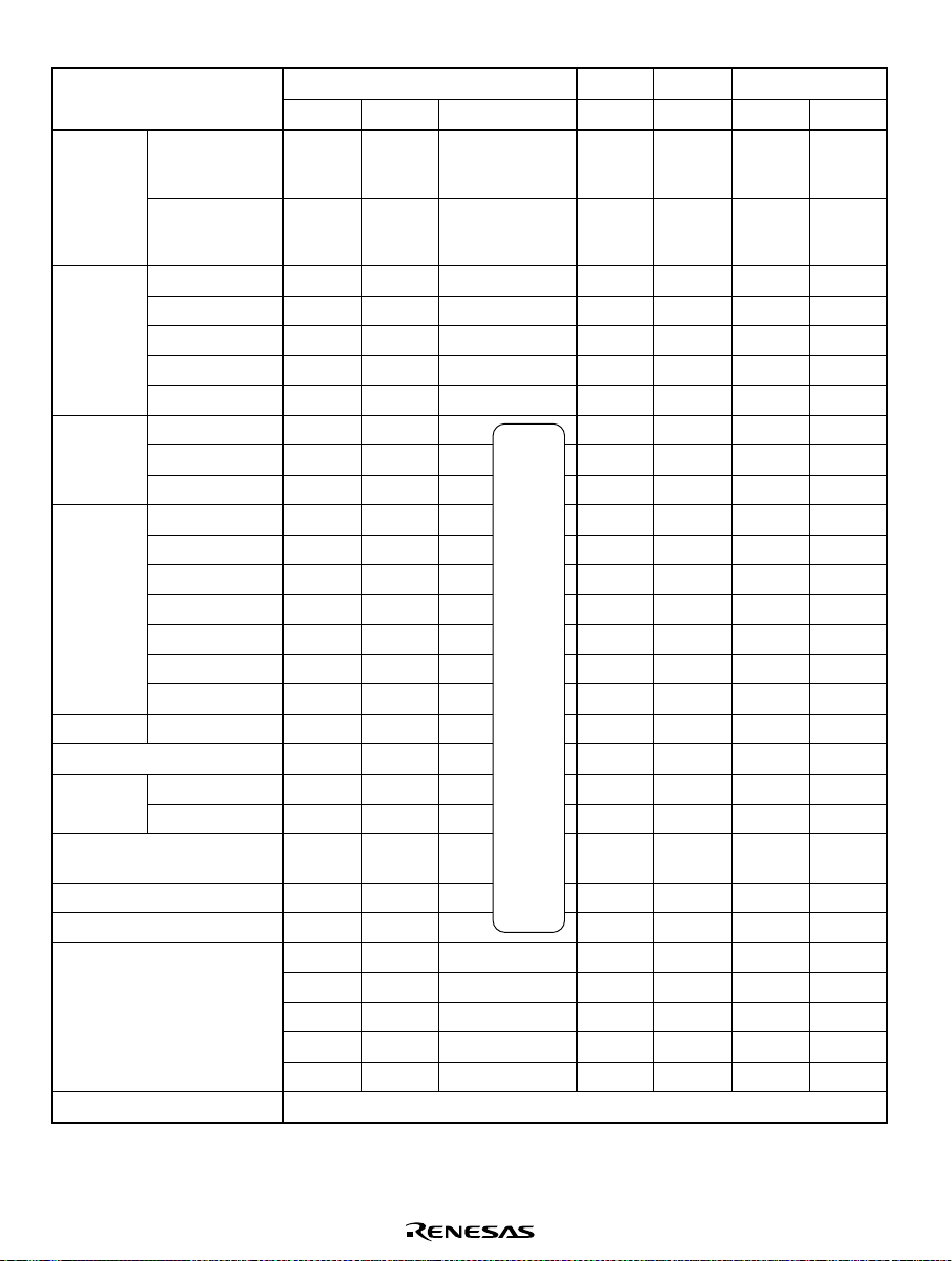
Below is a table listing the product specifications for each group.
Notes: 1. F-ZTAT is a trademark of Renesas Technology Corp.
2. ZTAT is a trademark of Renesas Technology Corp.
1
*
) and PROM (ZTAT™
2
*
). This makes it possible to design
Rev. 6.00, 08/04, page v of xxx
Page 6
Specifications
Item
Memory ROM 32 Kbytes 8 Kbytes
RAM 1 Kbyte 512 bytes
Operating
voltage and
operating
frequency
I/O portsInput only 999 9999
Timers Clock (timer A) 1 1 1 1 1 1 1
SCI UART/Synchronous 8 × 18 × 18 × 18 × 18 × 18 × 18 × 1
A-D 10 × 8 10 × 8 10 × 8 10 × 8 10 × 8 10 × 8 10 × 8
LCD seg 32 32 32 32 32 32 32
External interrupt (internal
wakeup)
POR (power-on reset) — — — — — 1 1
LVD (low-voltage detecti on ci rc ui t) — — — — — 1 1
Package FP-80A FP-80A FP-80A FP-80A FP-80A FP-80A FP-80A
Operating temperature Standard specifications: –20 to 70°C, WTR: –40 to 85°C
4.5 to 5.5 V 16 MHz 16 MHz — — — 16 MHz 16 MHz
2.7 to 5.5 V 10 MHz 10 MHz — — — 16 MHz 16 MHz
1.8 to 5.5 V 4 MHz 4 MHz — — — — —
2.7 to 3.6 V — — 10 MHz 10 MHz 10 MHz — —
1.8 to 3.6 V — — — — 4 MHz — —
Output only 6 6 6 6 6 6 6
I/O 515151 51515050
Reload (timer C) 1 1 1 1 1 1 1
Compare (timer F) 1 1 1 1 1 1 1
Capture (timer G) 1 1 1 1 1 1 1
AEC 111 1111
WDT 1 1 1 1 1
WDT (discrete) 11
com 444 4444
ZTAT Mask Flash Flash Mask Flash Mask
13(8) 13(8) 13(8) 13(8) 13(8) 13(8) 13(8)
FP-80B FP-80B FP-80B FP-80B
TFP-80C TFP-80C TFP-80C TFP-80C TFP-80C TFP-80C TFP-80C
38024 38024R 38024S 38124
to
32 Kbytes
or
1 Kbyte
Chip Chip Chip Chip
32 Kbytes 32 Kbytes 8 Kbytes
to
32 Kbytes
1 Kbyte 1 Kbyte 512 bytes
or
1 Kbyte
Please
use R
version.
TLP85V TLP85V TLP85V
32 Kbytes 8 Kbytes
to
32 Kbytes
1 Kbyte 512 bytes
or
1 Kbyte
Rev. 6.00, 08/04, page vi of xxx
Page 7

Target Readers: This manual is designed for use by people who design application systems using
the H8/38024 Group, H8/38024S Group, H8/38024F-ZTAT, and H8/38124 Group.
To use this manual, basic knowledge of electric circuits, logic circuits and microcomputers is
required.
Purpose: This manual provides the information of the hardware functions and electrical
characteristics of the H8/38024 Group, H8/38024S Group, H8/38024F-ZTAT, and H8/38124
Group. The H8/300L Series Programming Manual contains detailed information of executable
instructions. Please read the Programming Manual together with this manual.
How to Use the Book:
• To understa nd gene ra l fu nc tio n s
→ Read the manual from the beginning.
The manual explains the CPU, system control functions, peripheral functions and electrical
characteristics in that order.
• To understanding CPU functions
→ Refer to the separate H8/300L Series Programming Manual.
Explanatory Note: Bit sequence: upper bit at left, and lower bit at right
List of Related Documents: The latest documents are available on our Web site. Please make
sure that you have the late st version.
(http://www.renesas.com/)
• User manual for H8/38024 Group
Name of Document Document No.
H8/38024 Group, H8/38024S Group, H8/38024F-ZTAT™,
H8/38124 Group Hardware Manual
H8/300L Series Programming Manual ADE-602-040
This manual
• User manual for development tools
Name of Document Document No.
H8S, H8/300 Series, C/C++ Compiler, Assembler, Optimizing Linkage
Editor User’s Manual
High-Performance Debugging Interface User’s Manual ADE-702-161A
High-Performance Embedded Workshop ADE-702-201A
ADE-702-247
• Application note
Name of Document Document No.
H8/300 Series, H8/300L Series software ADE-502-052
Rev. 6.00, 08/04, page vii of xxx
Page 8

Notes: The following limitations apply to H8/38024 and H8/38124 programming and debugging
when the on-chip emulator is used.
1. Pin 95 is not available because it is used exclusively by the on-chip emulator.
2. Pins 33, 34, and 35 are unavailable for use. In order to use these pins additional
hardware must be mounted on the user board.
3. The address range H'7000 to H'7FFF is used by the on-chip emulator and is unavailable
to the user.
4. The address range H'F780 to H'FB7F must not be accessed under any circumstances.
5. When the on-chip emulator is being used, pin 95 is I/O, pins 33 and 34 are input, and
pin 35 is output.
6. When using the on-chip emulator, pins OSC1 and OSC2 should be connected to an
oscillator, or an external clock should be supplied to pin OSC1, even if the on-chip
oscillator of the H8/38124 Group is selected.
Rev. 6.00, 08/04, page viii of xxx
Page 9
List of Items Revised or Added for This Version
Item Page Revisions (See Manual for Details)
1.1 Overview
Table 1.1 Features
6 Table 1.1 amended
Product Code
Mask ROM Version ZTAT Version F-ZTAT Version Package
HD64338024 HD64738024 HD64F38024R
HD64338020 — — FP-80A
HD64F38024
FP-80A
FP-80B
TFP-80C
TLP-85V (HD64F38024R only)
Die (mask ROM/F-ZTAT version
only)
FP-80B
TFP-80C
Die
ROM/RAM Size
(Byte)
32K/1K
8K/512
3.4.2 Notes on
Rewriting Port Mode
Registers
Table 3.5 Conditions
under which Interrupt
Request Flag is Set
to 1
97 Table 3.5 amended
Interrupt Request
Flags Set to 1 Conditions
IWPR IWPF7
When PMR5 bit WKP7 is changed from 0 to 1 while pin
WKEGS7 = 0.
When PMR5 bit WK P 7 is changed fro m 1 to 0 while pin
WKEGS7 = 1.
IWPF6
When PMR5 bit WKP6 is changed from 0 to 1 while pin
WKEGS6 = 0.
When PMR5 bit WK P 6 is changed fro m 1 to 0 while pin
WKEGS6 = 1.
IWPF5
When PMR5 bit WKP5 is changed from 0 to 1 while pin
WKEGS5 = 0.
When PMR5 bit WK P 5 is changed fro m 1 to 0 while pin
WKEGS5 = 1.
IWPF4
When PMR5 bit WKP4 is changed from 0 to 1 while pin
WKEGS4 = 0.
When PMR5 bit WK P 4 is changed fro m 1 to 0 while pin
WKEGS4 = 1.
IWPF3
When PMR5 bit WKP3 is changed from 0 to 1 while pin
WKEGS3 = 0.
When PMR5 bit WK P 3 is changed fro m 1 to 0 while pin
WKEGS3 = 1.
IWPF2
When PMR5 bit WKP2 is changed from 0 to 1 while pin
WKEGS2 = 0.
When PMR5 bit WK P 2 is changed fro m 1 to 0 while pin
WKEGS2 = 1.
IWPF1
When PMR5 bit WKP1 is changed from 0 to 1 while pin
WKEGS1 = 0.
When PMR5 bit WK P 1 is changed fro m 1 to 0 while pin
WKEGS1 = 1.
IWPF0
When PMR5 bit WKP0 is changed from 0 to 1 while pin
WKEGS0 = 0.
When PMR5 bit WK P 0 is changed fro m 1 to 0 while pin
WKEGS0 = 1.
is low and WEGR bit
7
is low and WEGR bit
7
is low and WEGR bit
6
is low and WEGR bit
6
is low and WEGR bit
5
is low and WEGR bit
5
is low and WEGR bit
4
is low and WEGR bit
4
is low and WEGR bit
3
is low and WEGR bit
3
is low and WEGR bit
2
is low and WEGR bit
2
is low and WEGR bit
1
is low and WEGR bit
1
is low and WEGR bit
0
is low and WEGR bit
0
Rev. 6.00, 08/04, page ix of xxx
Page 10
Item Page Revisions (See Manual for Details)
4.1.1 Block Diagram
Figure 4.2 Block
Diagram of Clock Pulse
102 Figure 4.2 amended
(Before) Internal reset signal → (After) Internal reset signal
(other than watchdog timer or low-voltage detect circuit reset)
Generators (H8/38124
Group)
4.2 System Clock
Generator
105 Table 4.2
Frequency (MHz) 4 4.193
Table 4.2 Crystal
Oscillator Parameters
On-Chip Oscillator
Selection Method
(H8/38124 Group Only)
108 Note added
The on-chip oscillator is selected by setting the IRQAEC pin
input level during resets.*
* Other than watchdog timer or low-voltage detect circuit
reset.
4.4 Prescalers 111 Prescalers S (PPS)
Description amended
The output from prescaler S is shared by timer A,
timer G, SCI3, the A/D converter, the LCD controller,
F,
watchdog timer, and the 10-bit PWM. The divider ratio can be
set separately for each on-chip peripheral function.
4.5.1 Definition of
Oscillation Stabilization
Wait Time
5.1 Overview
Table 5.1 Operating
Modes
115 2. Wait time
Description amended, notes *1, *2 added
Oscillation stabilization wait time = oscillation stabilization time + wait time
Notes: 1. H8/38024 Group
2. H8/38124 Group
117 Table 5.1 amended
Operating Mode Description
Watch mode The CPU halts. The time-base function of timer A, timer F,
= t
+ (8 to 16,384 states)
rc
(to 131,072 states)
timer G, AEC and LCD controller/driver are operable on the
subclock
timer C, timer
1
*
................. (1)
2
*
Rev. 6.00, 08/04, page x of xxx
Page 11
Item Page Revisions (See Manual for Details)
8.1 Overview
Table 8.1 Port
Functions
187,
188
Table 8.1 amended
Port Description Pins Other Functions
Port 3
• 8-bit I/O port
• MOS input pull-up
• Large-current
• MOS open drain
option
2
*
port
output selectable
(only P3
5
P3
/AEVL
7
P3
/AEVH
6
P3
to P3
5
3
P32, TMOFH
, TMOFL
P3
1
P3
/UD Timer C count up/down
0
)
(Before) Input terminal → (After) input pin
8.9.1 Overview
Figure 8.8 Port
9 Pin
222 Figure 8.8 figure title amended
Configuration
9.2.1 Overview 238 Features
Description deleted
• Use of module standby mode enables this module to be
placed in standby mode independently when not used.
9.4.2 Register
Descriptions
258 Timer Control Register F (TCRF)
Bits 2 to—Clock Select L (CKSL2 to CKSL0)
Note * amended
Note: * …. Note that the timer F counter may increment if the
setting of IRQ3 in port mode register 1 (PMR1) is changed
0 to 1 or from 1 to 0 while the TMIF pin is low order to changed
the TMIF pin function.
9.6.1 Overview 290 Feature
• On-chip the H8/38/124 Group, 10 internal clocks (φ/64, φ/128,
φ/256, φ/512, φ/1024, φ/2048, φ/4096, φ/8192, φw/32, or
watchdog on-chip oscillator) are available for selection for use
by the counter.
Figure 9.17 (2) Block
Diagram of Watchdog
Timer (H8/38124
Group)
292 Block Diagram
Figure amended
(Before) On-chip oscillator → (After)
oscillator
Function
Switching
Registers
Asynchronous counter event
input pins AEVL, AEVH
None PMR2
Timer F output compare
output
selection input
PMR3
ECCR
PMR3
PMR3
Watchdog on-chip
from
Rev. 6.00, 08/04, page xi of xxx
Page 12

Item Page Revisions (See Manual for Details)
9.6.2 Register
Descriptions
297 Timer Mode Register (TMW)
Bits 3 to 0—Clock Select (CKS3 to CKS0)
Bit table amended
Bit 3
CKS3
Bit 2
CKS2
Bit 1
CKS1
Bit 0
CKS0 Description
0XXX
Watchdog on-chip oscillat or
9.7.2 Register
Configurations
309 Event Counter Control/Status Register (ECCSR)
Description amended
• Bit 7—Control
• Bit 6—Counter
9.7.3 Operation
Figure 9.22 Event
Counter Operation
Waveform
316 Event Counter PWM Operation
Figure 9.22 amended
Ndr: Value of ECPWDRH and ECPWDRL Fixed
= H’FFFF
14.1 Overview 423 Note * added
Note: * The voltage maintained in standby mode is the same as
the RAM data retaining voltage (VRAM). See section 16.8.2,
DC Characteristics, for information on retaining voltage.
14.2.1 Low-Voltage
Detection Control
Register (LVDCR)
428 Note added
Note: Setting values marked with an asterisk (*) are invalid.
Table 14.3 LVDCR
Settings and Function
Register Selections
14.2.2 Low-Voltage
Detection Status
Register (LVDSR)
14.3.2 Low-Voltage
Detection Circuit
LVDR (Reset by Low
Voltage Detect) Circuit:
428 Note amended
Note: * These bits
432 Description amended
To operate the LVDR, set the LVDE bit in LVDCR to 1, wait for
150 µs (t
LVDON
detection power supply have stabilized, based on overflow of
LVDNT, etc., then set the LVDRE bit in LVDCR to 1.
LVDI (Interrupt by Low
Voltage Detect) Circuit:
433 Description amended
To operate the LVDI, set the LVDE bit in LVDCR to 1, wait for
150 µs (t
LVDON
detection power supply have stabilized, based on overflow of
LVDNT, etc., then set the LVDDE and LVDUE bits in LVDCR to
1.
Overflow H (OVH)
Overflow L (OVL)
low when Ndr
initialized by resets trigged by LVDR.
) until the reference voltage and the low-voltage-
) until the reference voltage and the low-voltage-
Rev. 6.00, 08/04, page xii of xxx
Page 13

Item Page Revisions (See Manual for Details)
14.3.2 Low-Voltage
Detection Circuit
Operation and
Cancellation Setting
Procedure Using LVDR
437 Description amended
2. After waiting for LVDCNT overflow, etc., to ensure that the
stabilization time (t
and low voltage detection power supply has elapsed, clear
bits LVDDF and LVDUF in LVDSR to 0.
= 150 µs) for the reference voltage
LVDON
and LVDI:
16.4.2 DC
Characteristics
Table 16.8 DC
Characteristics
16.8.1 Power Supply
462 Table amended
Item Sym bol Applicable Pi ns Min Typ Max Unit Test Condit i on Not es
output low
current
(per pin)
IOLOutput pins
except port 9
P9
P93 to P9
487 Figure amended
to P9
0
Values
——0.5 mAAllowable
— — 25.0 mA
2
— — 10.0
— — 10.0 mA
5
Voltage and Operating
Ranges
Power Supply Voltage
and Oscillation
Frequency Range (OnChip Oscillator
Selected)
1
*
2
*
5
*
Rev. 6.00, 08/04, page xiii of xxx
Page 14
Item Page Revisions (See Manual for Details)
16.8.1 Power Supply
490 Figure amended
Voltage and Operating
Ranges
1.0
Analog Power Supply
Voltage and A/D
Converter Operating
Range (On-Chip
Oscillator Selected)
16.8.2 DC
Characteristics
Table 16.21 DC
Characteristics
492 Table 16.21 amended
φ (MHz)
0.35
2.7 5.5
AV
CC (V)
• Active (high-speed) mode
• Sleep (high-speed) mode
Item Symbol Applicable Pins Min Typ Max Unit Test Condition Notes
V
Output
high
voltage
OH
P13, P14, P17,
P3
to P37,
0
P4
to P42,
0
P5
to P57,
0
to P67,
P6
0
P7
to P77,
0
P8
to P87,
0
PA
to PA
0
3
Values
VCC – 1.0 — — V VCC = 4.0 V to 5.5 V
V
– 0.5 — — VCC = 4.0 V to 5.5 V
CC
VCC – 0.3 — — –IOH = 0.1 mA
493 Table 16.21 amended
Item Symbol Applicable Pins Min Typ Max Unit Test Condition Notes
Output low
V
P90 to P9
voltage
Pull-up
MOS
current
OL
–I
p
P1
3
P3
0
P5
0
P6
0
5
, P14, P17,
to P37,
to P57,
to P6
7
Values
——1.5 VCC = 4.0 V to 5.5 V
——1.0 V
20 — 200 µAVVCC = 5.0 V,
— 40 — VCC = 2.7 V,
= 1.0 mA
–I
OH
= 0.5 mA
–I
OH
= 15 mA
I
OL
= 4.0 V to 5.5 V
CC
= 10 mA
I
OL
= 0.0 V
V
IN
V
= 0.0 V
IN
Reference
value
Rev. 6.00, 08/04, page xiv of xxx
Page 15

Item Page Revisions (See Manual for Details)
16.8.2 DC
Characteristics
Table 16.21 DC
Characteristics
497 to
499
Table 16.21 amended, note *6 added
Item Symbol Applicable Pins Min Typ Max Unit Test Condition Notes
I
Watch
WATCHVCC
mode
current
consumption
I
Standby
STBYVCC
mode
current
consumption
V
RAM
RAM data
retaining
voltage
V
CC
Values
— TBD — µA
— 1.8 —
— 1.8 6.0 VCC = 2.7 V,
— TBD — µA
— 0.5 —
— 0.05 — VCC = 2.7 V,
— 0.6 — VCC = 5.0 V,
— 0.16 —
— 1.0 5.0
2.0 —— V
VCC = 2.7 V,
T
= 25°C,
a
32-kHz crystal
resonator used,
LCD not used
32-kHz crystal
resonator used,
LCD not used
V
= 2.7 V,
CC
T
= 25°C,
a
32-kHz crystal
resonator not used
= 2.7 V,
V
CC
T
= 25°C,
a
32-kHz crystal
resonator not used
T
= 25°C,
a
SUBSTP (subclock
oscillator control
register) setting = 1
T
= 25°C,
a
32-kHz crystal
resonator not used
= 5.0 V,
V
CC
T
= 25°C,
a
SUBSTP (subclock
oscillator control
register) setting = 1
32-kHz crystal
resonator not used
1 *3 *4
*
Reference
value
2 *3 *4
*
Reference
value
3 *4
*
1 *3 *4
*
Reference
value
2 *3 *4
*
Reference
value
2 *4
*
Reference
value
2 *3 *4
*
Reference
value
4
*2 *
Reference
value
3 *4
*
6
*
Item Symbol
Allowable output low
current (per pin)
I
OL
Applicable
Pins Min Typ Max Unit
Output pins
except ports 3
and 9
Values
——2.0 mA
Port 3 ——10.0
Output pins
except port 9
——0.5
Port 9 ——15.0
——10.0
——8.0
Note: 6. Voltage maintained in standby mode
Rev. 6.00, 08/04, page xv of xxx
Test
Condition Notes
VCC = 4.0 V to
5.5 V
= 4.0 V to
V
CC
5.5 V
5
= 4.0 V to
*
V
CC
5.5 V
Page 16

Item Page Revisions (See Manual for Details)
16.8.3 AC
Characteristics
Table 16.22 Control
Signal Timing
500,
501
Table 16.22 amended, note *2 added
Item Symbol
System clock
oscillation
frequency
OSC clock (φ
cycle time
System clock (φ)
cycle time
f
OSC
)
t
OSC
OSC
t
cyc
Applicable
Pins Min Typ Max Unit Test Condition
OSC1, OSC
OSC1, OSC262.5 — 500 ns F igure 16.1
Values
2.0 — 16.0
2
0.7 — 2.0 On-chip oscillator
500 — 1429 On-chip oscillator
2 — 128 t
—— 182 µs
Note: 2. These characteristics are given as ranges between
minimum and maximum values in order to account for factors
such as temperature, power supply voltage, and variation
among production lots. When designing systems, make sure to
give due consideration to the SPEL range. Please see the Web
site for this product for actual performance data.
16.8.5 LCD
Characteristics
Table 16.25 LCD
Characteristics
503 Table 16.25 amended
Applicable
Item Symbol
Liquid crystal
display volt age
V
LCDV1
Pins
Values
Min Typ Max Unit Test Condition
2.7 — 5.5 V
MHz
OSC
selected
selected
Reference
Figure
2
*
Reference
Figure
2
*
16.8.7 Power Supply
506 Table 16.27
Voltage Detection
Circuit Characteristics
Table 16.27 Power
Item Symbol Min Typ Max Unit Test Conditions
LVD stabilization time T
150 ——µs
LVDON
Supply Voltage
Detection Circuit
Characteristics (1)
16.8.8 Power-On
509 Title amended
Reset Circuit
Characteristics
B.2 Functions 574 PWCR1—PWM1 Control Register
Note 1 amended
Notes: 1. tφ: Period of
PWM1 input clock
589 OSCCR—Clock Pulse Generator Control Register
Bit table amended
2
IRQAECF
R
1
OSCF
R
0
0
R/W
Rated Values
Rev. 6.00, 08/04, page xvi of xxx
Page 17
Item Page Revisions (See Manual for Details)
E. List of Product
Codes
Table E.1 H8/38024
Group Product Code
Lineup
618 Table E.1 amended
Product Type Product Code Mark Code
H8/38124 HD64F38124H F38124H 80-pin QFP (FP-80A)
H8/38124
Group
F-ZTAT
versions
Mask ROM
versions
H8/38123 HD64338123H 38123(***)H 80-pin QFP (FP-80A)Mask ROM
versions
H8/38122 HD64338122H 38122(***)H 80-pin QFP (FP-80A)Mask ROM
versions
H8/38121 HD64338121H 38121(***)H 80-pin QFP (FP-80A)
Mask ROM
versions
H8/38120 HD64338120H 38120(***)H 80-pin QFP (FP-80A)Mask ROM
versions
Regular
specifications
Wide-range
specifications
Regular
specifications
specifications
Regular
specifications
specifications
Regular
specifications
Wide-range
specifications
Regular
specifications
Wide-range
specifications
Regular
specifications
specifications
HD64F38124W F38124W 80-pin TQFP (TFP-80C)
HD64F38124HW F38124H 80-pin QFP (FP-80A)
HD64F38124WW F38124W 80-pin TQFP (TFP-80C)
HD64338124H 38124(***)H 80-pin QFP (FP-80A)
HD64338124W 38124(***) 80-pin TQFP (TFP-80C)
HD64338124HW 38124(***)H 80-pin QFP (FP-80A)Wide-range
HD64338124WW 38124(***) 80-pin TQFP (TFP-80C)
HD64338123W 38123(***) 80-pin TQFP (TFP-80C)
HD64338123HW 38123(***)H 80-pin QFP (FP-80A)Wide-range
HD64338123WW 38123(***) 80-pin TQFP (TFP-80C)
HD64338122W 38122(***) 80-pin TQFP (TFP-80C)
HD64338122HW 38122(***)H 80-pin QFP (FP-80A)
HD64338122WW 38122(***) 80-pin TQFP (TFP-80C)
HD64338121W 38121(***) 80-pin TQFP (TFP-80C)
HD64338121HW 38121(***)H 80-pin QFP (FP-80A)
HD64338121WW 38121(***) 80-pin TQFP (TFP-80C)
HD64338120W 38120(***) 80-pin TQFP (TFP-80C)
HD64338120HW 38120(***)H 80-pin QFP (FP-80A)Wide-range
HD64338120WW 38120(***) 80-pin TQFP (TFP-80C)
Package
(Package Code)
Rev. 6.00, 08/04, page xvii of xxx
Page 18

Rev. 6.00, 08/04, page xviii of xxx
Page 19

Contents
Section 1 Overview............................................................................................................. 1
1.1 Overview........................................................................................................................... 1
1.2 Internal Block Diagram..................................................................................................... 7
1.3 Pin Arrangement and Functions........................................................................................ 9
1.3.1 Pin Arrangement.................................................................................................. 9
1.3.2 Pin Functions ....................................................................................................... 19
Section 2 CPU...................................................................................................................... 25
2.1 Overview........................................................................................................................... 25
2.1.1 Features................................................................................................................ 25
2.1.2 Address Space...................................................................................................... 26
2.1.3 Register Configuration......................................................................................... 26
2.2 Register Descriptions........................................................................................................27
2.2.1 General Registers................................................................................................. 27
2.2.2 Control Registers ................................................................................................. 27
2.2.3 Initial Register Values.......................................................................................... 29
2.3 Data Formats..................................................................................................................... 29
2.3.1 Data Formats in General Registers ...................................................................... 30
2.3.2 Memory Data Formats......................................................................................... 31
2.4 Addressing Modes.............................................................................................................32
2.4.1 Addressing Modes............................................................................................... 32
2.4.2 Effective Address Calculation.............................................................................. 34
2.5 Instruction Set................................................................................................................... 38
2.5.1 Data Transfer Instructions.................................................................................... 40
2.5.2 Arithmetic Operations.......................................................................................... 42
2.5.3 Logic Operations.................................................................................................. 43
2.5.4 Shift Operations................................................................................................... 43
2.5.5 Bit Manipulations................................................................................................. 45
2.5.6 Branching Instructions......................................................................................... 49
2.5.7 System Control Instructions................................................................................. 51
2.5.8 Block Data Transfer Instruction........................................................................... 52
2.6 Basic Operational Timing................................................................................................. 54
2.6.1 Access to On-Chip Memory (RAM, ROM)......................................................... 54
2.6.2 Access to On-Chip Peripheral Modules............................................................... 55
2.7 CPU States........................................................................................................................ 57
2.7.1 Overview.............................................................................................................. 57
2.7.2 Program Execution State...................................................................................... 58
2.7.3 Program Halt State............................................................................................... 58
2.7.4 Exception-Handling State.................................................................................... 58
Rev. 6.00, 08/04, page xix of xxx
Page 20

2.8 Memory Map .................................................................................................................... 59
2.8.1 Memory Map....................................................................................................... 59
2.9 Application Notes ............................................................................................................. 64
2.9.1 Notes on Data Access.......................................................................................... 64
2.9.2 Notes on Bit Manipulation................................................................................... 66
2.9.3 Notes on Use of the EEPMOV Instruction.......................................................... 72
Section 3 Exception Handling......................................................................................... 73
3.1 Overview........................................................................................................................... 73
3.2 Reset.................................................................................................................................. 73
3.2.1 Overview.............................................................................................................. 73
3.2.2 Reset Sequence.................................................................................................... 73
3.2.3 Interrupt Immediately after Reset........................................................................ 74
3.3 Interrupts........................................................................................................................... 75
3.3.1 Overview.............................................................................................................. 75
3.3.2 Interrupt Control Registers.................................................................................. 77
3.3.3 External Interrupts............................................................................................... 87
3.3.4 Internal Interrupts ................................................................................................ 88
3.3.5 Interrupt Operations............................................................................................. 89
3.3.6 Interrupt Response Time...................................................................................... 94
3.4 Application Notes ............................................................................................................. 95
3.4.1 Notes on Stack Area Use..................................................................................... 95
3.4.2 Notes on Rewriting Port Mode Registers............................................................. 96
3.4.3 Method for Clearing Interrupt Request Flags ...................................................... 98
Section 4 Clock Pulse Generators................................................................................... 101
4.1 Overview........................................................................................................................... 101
4.1.1 Block Diagram..................................................................................................... 101
4.1.2 System Clock and Subclock................................................................................. 102
4.1.3 Register Descriptions........................................................................................... 102
4.2 System Clock Generator................................................................................................... 104
4.3 Subclock Generator........................................................................................................... 109
4.4 Prescalers.......................................................................................................................... 111
4.5 Note on Oscillators ........................................................................................................... 112
4.5.1 Definition of Oscillation Stabilization Wait Time............................................... 113
4.5.2 Notes on Use of Crystal Oscillator Element (Excl uding Ceramic Oscillator
Element)............................................................................................................... 115
4.5.3 Note on Use of HD64F38024.............................................................................. 116
4.6 Notes on H8/38124 Group................................................................................................ 116
Section 5 Power-Down Modes........................................................................................ 117
5.1 Overview........................................................................................................................... 117
5.1.1 System Control Registers..................................................................................... 120
Rev. 6.00, 08/04, page xx of xxx
Page 21

5.2 Sleep Mode ....................................................................................................................... 124
5.2.1 Transition to Sleep Mode..................................................................................... 124
5.2.2 Clearing Sleep Mode............................................................................................ 125
5.2.3 Clock Frequency in Sleep (Medium-Speed) Mode.............................................. 125
5.3 Standby Mode................................................................................................................... 126
5.3.1 Transition to Standby Mode................................................................................. 126
5.3.2 Clearing Standby Mode....................................................................................... 126
5.3.3 Oscillator Stabilization Time after Standby Mode is Cleared.............................. 127
5.3.4 Standby Mode Transition and Pin States............................................................. 128
5.3.5 Notes on External Input Signal Changes before/after Standby Mode.................. 129
5.4 Watch Mode...................................................................................................................... 131
5.4.1 Transition to Watch Mode................................................................................... 131
5.4.2 Clearing Watch Mode.......................................................................................... 131
5.4.3 Oscillator StabilizationTime after Watch Mode is Cleared ................................. 131
5.4.4 Notes on External Input Signal Changes before/after Watch Mode .................... 131
5.5 Subsleep Mode.................................................................................................................. 132
5.5.1 Transition to Subsleep Mode............................................................................... 132
5.5.2 Clearing Subsleep Mode...................................................................................... 132
5.6 Subactive Mode ................................................................................................................ 133
5.6.1 Transition to Subactive Mode.............................................................................. 133
5.6.2 Clearing Subactive Mode..................................................................................... 133
5.6.3 Operating Frequency in Subactive Mode............................................................. 133
5.7 Active (Medium-Speed) Mode ......................................................................................... 134
5.7.1 Transition to Active (Medium-Speed) Mode....................................................... 134
5.7.2 Clearing Active (Medium-Speed) Mode.............................................................. 134
5.7.3 Operating Frequency in Active (Medium-Speed) Mode...................................... 134
5.8 Direct Transfer.................................................................................................................. 135
5.8.1 Overview of Direct Transfer................................................................................ 135
5.8.2 Direct Transition Times....................................................................................... 136
5.8.3 Notes on External Input Signal Changes before/after Direct Transition.............. 138
5.9 Module Standby Mode...................................................................................................... 139
5.9.1 Setting Module Standby Mode ............................................................................ 139
5.9.2 Clearing Module Standby Mode.......................................................................... 139
Section 6 ROM..................................................................................................................... 141
6.1 Overview........................................................................................................................... 141
6.1.1 Block Diagram..................................................................................................... 141
6.2 H8/38024 PROM Mode.................................................................................................... 142
6.2.1 Setting to PROM Mode ....................................................................................... 142
6.2.2 Socket Adapter Pin Arrangement and Memory Map........................................... 142
6.3 H8/38024 Programming.................................................................................................... 145
6.3.1 Writing and Verifying.......................................................................................... 145
6.3.2 Programming Precautions.................................................................................... 150
Rev. 6.00, 08/04, page xxi of xxx
Page 22

6.4 Reliability of Programmed Data....................................................................................... 151
6.5 Flash Memory Overview .................................................................................................. 152
6.5.1 Features................................................................................................................ 152
6.5.2 Block Diagram..................................................................................................... 153
6.5.3 Block Configuration............................................................................................. 154
6.5.4 Register Configuration......................................................................................... 155
6.6 Descriptions of Registers of the Flash Memory................................................................ 156
6.6.1 Flash Memory Control Register 1 (FLMCR1)..................................................... 156
6.6.2 Flash Memory Control Register 2 (FLMCR2)..................................................... 158
6.6.3 Erase Block Register (EBR)................................................................................ 159
6.6.4 Flash Memory Power Control Register (FLPWCR)............................................ 159
6.6.5 Flash Memory Enable Register (FENR).............................................................. 160
6.7 On-Board Programming Modes........................................................................................ 161
6.7.1 Boot Mode........................................................................................................... 162
6.7.2 Programming/Erasing in User Program Mode..................................................... 164
6.7.3 Notes on On-Board Programming ....................................................................... 165
6.8 Flash Memory Programming/Erasing............................................................................... 165
6.8.1 Program/Program-Verify..................................................................................... 165
6.8.2 Erase/Erase-Verify............................................................................................... 169
6.8.3 Interrupt Handling when Programming/Erasing Flash Memory.......................... 169
6.9 Program/Erase Protection ................................................................................................. 171
6.9.1 Hardware Protection............................................................................................ 171
6.9.2 Software Protection.............................................................................................. 171
6.9.3 Error Protection.................................................................................................... 171
6.10 Programmer Mode ............................................................................................................ 172
6.10.1 Socket Adapter..................................................................................................... 172
6.10.2 Programmer Mode Commands............................................................................ 172
6.10.3 Memory Read Mode............................................................................................ 175
6.10.4 Auto-Program Mode............................................................................................ 178
6.10.5 Auto-Erase Mode................................................................................................. 180
6.10.6 Status Read Mode................................................................................................ 181
6.10.7 Status Polling....................................................................................................... 183
6.10.8 Programmer Mode Transition Time .................................................................... 183
6.10.9 Notes on Memory Programming.......................................................................... 184
6.11 Power-Down States for Flash Memory............................................................................. 184
Section 7 RAM..................................................................................................................... 185
7.1 Overview........................................................................................................................... 185
7.1.1 Block Diagram..................................................................................................... 185
Section 8 I/O Ports.............................................................................................................. 187
8.1 Overview........................................................................................................................... 187
8.2 Port 1................................................................................................................................. 189
Rev. 6.00, 08/04, page xxii of xxx
Page 23

8.2.1 Overview.............................................................................................................. 189
8.2.2 Register Configuration and Description............................................................... 189
8.2.3 Pin Functions ....................................................................................................... 194
8.2.4 Pin States.............................................................................................................. 195
8.2.5 MOS Input Pull-Up.............................................................................................. 195
8.3 Port 3................................................................................................................................. 196
8.3.1 Overview.............................................................................................................. 196
8.3.2 Register Configuration and Description............................................................... 196
8.3.3 Pin Functions ....................................................................................................... 201
8.3.4 Pin States.............................................................................................................. 202
8.3.5 MOS Input Pull-Up.............................................................................................. 202
8.4 Port 4................................................................................................................................. 203
8.4.1 Overview.............................................................................................................. 203
8.4.2 Register Configuration and Description............................................................... 203
8.4.3 Pin Functions ....................................................................................................... 205
8.4.4 Pin States.............................................................................................................. 206
8.5 Port 5................................................................................................................................. 207
8.5.1 Overview.............................................................................................................. 207
8.5.2 Register Configuration and Description............................................................... 207
8.5.3 Pin Functions ....................................................................................................... 210
8.5.4 Pin States.............................................................................................................. 211
8.5.5 MOS Input Pull-Up.............................................................................................. 211
8.6 Port 6................................................................................................................................. 212
8.6.1 Overview.............................................................................................................. 212
8.6.2 Register Configuration and Description............................................................... 212
8.6.3 Pin Functions ....................................................................................................... 214
8.6.4 Pin States.............................................................................................................. 215
8.6.5 MOS Input Pull-Up.............................................................................................. 215
8.7 Port 7................................................................................................................................. 216
8.7.1 Overview.............................................................................................................. 216
8.7.2 Register Configuration and Description............................................................... 216
8.7.3 Pin Functions ....................................................................................................... 218
8.7.4 Pin States.............................................................................................................. 218
8.8 Port 8................................................................................................................................. 219
8.8.1 Overview.............................................................................................................. 219
8.8.2 Register Configuration and Description............................................................... 219
8.8.3 Pin Functions ....................................................................................................... 221
8.8.4 Pin States.............................................................................................................. 221
8.9 Port 9................................................................................................................................. 222
8.9.1 Overview.............................................................................................................. 222
8.9.2 Register Configuration and Description............................................................... 222
8.9.3 Pin Functions ....................................................................................................... 225
8.9.4 Pin States.............................................................................................................. 225
Rev. 6.00, 08/04, page xxiii of xxx
Page 24

8.10 Port A................................................................................................................................ 226
8.10.1 Overview.............................................................................................................. 226
8.10.2 Register Configuration and Description............................................................... 226
8.10.3 Pin Functions....................................................................................................... 228
8.10.4 Pin States ............................................................................................................. 229
8.11 Port B................................................................................................................................ 230
8.11.1 Overview.............................................................................................................. 230
8.11.2 Register Configuration and Description............................................................... 230
8.11.3 Pin Functions....................................................................................................... 232
8.12 Input/Output Data Inversion Function.............................................................................. 233
8.12.1 Overview.............................................................................................................. 233
8.12.2 Register Configuration and Descriptions............................................................. 234
8.12.3 Note on Modification of Serial Port Control Register......................................... 235
8.13 Application Note............................................................................................................... 236
8.13.1 The Management of the Un-Use Terminal.......................................................... 236
Section 9 Timers.................................................................................................................. 237
9.1 Overview........................................................................................................................... 237
9.2 Timer A............................................................................................................................. 238
9.2.1 Overview.............................................................................................................. 238
9.2.2 Register Descriptions........................................................................................... 240
9.2.3 Timer Operation................................................................................................... 243
9.2.4 Timer A Operation States.................................................................................... 243
9.2.5 Application Note.................................................................................................. 244
9.3 Timer C............................................................................................................................. 244
9.3.1 Overview.............................................................................................................. 244
9.3.2 Register Descriptions........................................................................................... 246
9.3.3 Timer Operation................................................................................................... 249
9.3.4 Timer C Operation States..................................................................................... 251
9.4 Timer F ............................................................................................................................. 252
9.4.1 Overview.............................................................................................................. 252
9.4.2 Register Descriptions........................................................................................... 255
9.4.3 CPU Interface ...................................................................................................... 262
9.4.4 Operation............................................................................................................. 265
9.4.5 Application Notes................................................................................................ 268
9.5 Timer G............................................................................................................................. 271
9.5.1 Overview.............................................................................................................. 271
9.5.2 Register Descriptions........................................................................................... 273
9.5.3 Noise Canceler..................................................................................................... 278
9.5.4 Operation............................................................................................................. 280
9.5.5 Application Notes................................................................................................ 284
9.5.6 Timer G Application Example............................................................................. 289
9.6 Watchdog Timer............................................................................................................... 290
Rev. 6.00, 08/04, page xxiv of xxx
Page 25

9.6.1 Overview.............................................................................................................. 290
9.6.2 Register Descriptions........................................................................................... 293
9.6.3 Timer Operation................................................................................................... 299
9.6.4 Watchdog Timer Operation States....................................................................... 300
9.7 Asynchronous Event Counter (AEC)................................................................................ 301
9.7.1 Overview.............................................................................................................. 301
9.7.2 Register Configurations....................................................................................... 304
9.7.3 Operation ............................................................................................................. 313
9.7.4 Asynchronous Event Counter Operation Modes.................................................. 317
9.7.5 Application Notes................................................................................................ 318
Section 10 Serial Communication Interface................................................................ 319
10.1 Overview........................................................................................................................... 319
10.1.1 Features................................................................................................................ 319
10.1.2 Block Diagram..................................................................................................... 321
10.1.3 Pin Configuration................................................................................................. 322
10.1.4 Register Configuration......................................................................................... 322
10.2 Register Descriptions........................................................................................................ 323
10.2.1 Receive Shift Register (RSR) .............................................................................. 323
10.2.2 Receive Data Register (RDR).............................................................................. 323
10.2.3 Transmit Shift Register (TSR)............................................................................. 324
10.2.4 Transmit Data Register (TDR)............................................................................. 324
10.2.5 Serial Mode Register (SMR)................................................................................ 325
10.2.6 Serial Control Register 3 (SCR3)......................................................................... 328
10.2.7 Serial Status Register (SSR) ................................................................................ 332
10.2.8 Bit Rate Register (BRR) ...................................................................................... 336
10.2.9 Clock stop register 1 (CKSTPR1)........................................................................ 342
10.2.10 Serial Port Control Register (SPCR).................................................................... 342
10.3 Operation........................................................................................................................... 344
10.3.1 Overview.............................................................................................................. 344
10.3.2 Operation in Asynchronous Mode....................................................................... 348
10.3.3 Operation in Synchronous Mode ......................................................................... 357
10.3.4 Multiprocessor Communication Function............................................................ 364
10.4 Interrupts........................................................................................................................... 371
10.5 Application Notes ............................................................................................................. 372
Section 11 10-Bit PWM..................................................................................................... 377
11.1 Overview........................................................................................................................... 377
11.1.1 Features................................................................................................................ 377
11.1.2 Block Diagram..................................................................................................... 378
11.1.3 Pin Configuration................................................................................................. 379
11.1.4 Register Configuration......................................................................................... 380
11.2 Register Descriptions........................................................................................................ 380
Rev. 6.00, 08/04, page xxv of xxx
Page 26

11.2.1 PWM Control Register (PWCRm) ...................................................................... 380
11.2.2 PWM Data Registers U and L (PWDRUm, PWDRLm) ..................................... 382
11.2.3 Clock Stop Register 2 (CKSTPR2)...................................................................... 383
11.3 Operation .......................................................................................................................... 384
11.3.1 Operation............................................................................................................. 384
11.3.2 PWM Operation Modes....................................................................................... 385
Section 12 A/D Converter................................................................................................. 387
12.1 Overview........................................................................................................................... 387
12.1.1 Features................................................................................................................ 387
12.1.2 Block Diagram..................................................................................................... 388
12.1.3 Pin Configuration................................................................................................. 389
12.1.4 Register Configuration......................................................................................... 389
12.2 Register Descriptions........................................................................................................ 390
12.2.1 A/D Result Registers (ADRRH, ADRRL)........................................................... 390
12.2.2 A/D Mode Register (AMR)................................................................................. 390
12.2.3 A/D Start Register (ADSR) ................................................................................. 392
12.2.4 Clock Stop Register 1 (CKSTPR1)...................................................................... 393
12.3 Operation .......................................................................................................................... 394
12.3.1 A/D Conversion Operation.................................................................................. 394
12.3.2 Start of A/D Conversion by External Trigger Input............................................. 394
12.3.3 A/D Converter Operation Modes......................................................................... 395
12.4 Interrupts........................................................................................................................... 395
12.5 Typical Use....................................................................................................................... 395
12.6 A/D Conversion Accuracy Definitions............................................................................. 398
12.7 Application Notes ............................................................................................................. 400
12.7.1 Application Notes ................................................................................................ 400
12.7.2 Permissible Signal Source Impedance................................................................. 400
12.7.3 Influences on Absolute Precision......................................................................... 400
Section 13 LCD Controller/Driver................................................................................. 403
13.1 Overview........................................................................................................................... 403
13.1.1 Features................................................................................................................ 403
13.1.2 Block Diagram..................................................................................................... 404
13.1.3 Pin Configuration................................................................................................. 406
13.1.4 Register Configuration......................................................................................... 406
13.2 Register Descriptions........................................................................................................ 407
13.2.1 LCD Port Control Register (LPCR)..................................................................... 407
13.2.2 LCD Control Register (LCR)............................................................................... 409
13.2.3 LCD Control Register 2 (LCR2).......................................................................... 411
13.2.4 Clock Stop Register 2 (CKSTPR2)...................................................................... 413
13.3 Operation .......................................................................................................................... 414
13.3.1 Settings up to LCD Display................................................................................. 414
Rev. 6.00, 08/04, page xxvi of xxx
Page 27

13.3.2 Relationship between LCD RAM and Display.................................................... 416
13.3.3 Operation in Power-Down Modes ....................................................................... 421
13.3.4 Boosting the LCD Drive Power Supply............................................................... 422
Section 14 Power-On Reset and Low-Voltage Detection Circuits
(H8/38124 Group Only)............................................................................... 423
14.1 Overview........................................................................................................................... 423
14.1.1 Features................................................................................................................ 423
14.1.2 Block Diagram..................................................................................................... 424
14.1.3 Pin Description..................................................................................................... 425
14.1.4 Register Descriptions........................................................................................... 425
14.2 Individual Register Descriptions....................................................................................... 425
14.2.1 Low-Voltage Detection Control Register (LVDCR) ........................................... 425
14.2.2 Low-Voltage Detection Status Register (LVDSR).............................................. 428
14.2.3 Low-Voltage Detection Counter (LVDCNT)...................................................... 430
14.2.4 Clock Stop Register 2 (CKSTPR2)...................................................................... 430
14.3 Operation........................................................................................................................... 431
14.3.1 Power-On Reset Circuit....................................................................................... 431
14.3.2 Low-Voltage Detection Circuit............................................................................ 432
Section 15 Power Supply Circuit (H8/38124 Group Only)..................................... 439
15.1 When Using Internal Power Supply Step-Down Circuit................................................... 439
15.2 When Not Using Internal Power Supply Step-Down Circuit............................................ 440
Section 16 Electrical Characteristics.............................................................................. 441
16.1 H8/38024 ZTAT Version and Mask ROM Version Absolute Maximum Ratings............ 441
16.2 H8/38024 ZTAT Version and Mask ROM Version Electrical Characteristics................. 442
16.2.1 Power Supply Voltage and Operating Range....................................................... 442
16.2.2 DC Characteristics............................................................................................... 444
16.2.3 AC Characteristics............................................................................................... 450
16.2.4 A/D Converter Characteristics............................................................................. 453
16.2.5 LCD Characteristics ............................................................................................. 454
16.3 H8/38024 F-ZTAT Version and H8/38024R F-ZTAT Version Absolute Maximum
Ratings.............................................................................................................................. 455
16.4 H8/38024 F-ZTAT Version and H8/38024R F-ZTAT Version Electrical Characteristics 456
16.4.1 Power Supply Voltage and Operating Range....................................................... 456
16.4.2 DC Characteristics............................................................................................... 458
16.4.3 AC Characteristics............................................................................................... 464
16.4.4 A/D Converter Characteristics............................................................................. 467
16.4.5 LCD Characteristics ............................................................................................. 468
16.4.6 Flash Memory Characteristics.............................................................................. 469
16.5 H8/38024S Group Mask ROM Version Absolute Maximum Ratings.............................. 471
16.6 H8/38024S Group Mask ROM Version Electrical Characteristics................................... 472
Rev. 6.00, 08/04, page xxvii of xxx
Page 28

16.6.1 Power Supply Voltage and Operating Range....................................................... 472
16.6.2 DC Characteristics............................................................................................... 474
16.6.3 AC Characteristics............................................................................................... 481
16.6.4 A/D Converter Characteristics............................................................................. 484
16.6.5 LCD Characteristics............................................................................................. 485
16.7 Absolute Maximum Ratings of H8/38124 Group............................................................. 486
16.8 Electrical Characteristics of H8/38124 Group.................................................................. 487
16.8.1 Power Supply Voltage and Operating Ranges..................................................... 487
16.8.2 DC Characteristics............................................................................................... 491
16.8.3 AC Characteristics............................................................................................... 500
16.8.4 A/D Converter Characteristics............................................................................. 502
16.8.5 LCD Characteristics............................................................................................. 503
16.8.6 Flash Memory Characteristics ............................................................................. 504
16.8.7 Power Supply Voltage Detection Circuit Characteristics.................................... 506
16.8.8 Power-On Reset Circuit Characteristics .............................................................. 509
16.8.9 Watchdog Timer Characteristics.......................................................................... 510
16.9 Operation Timing.............................................................................................................. 510
16.10 Output Load Circuit.......................................................................................................... 513
16.11 Resonator Equivalent Circuit............................................................................................ 513
16.12 Usage Note........................................................................................................................ 514
Appendix A CPU Instruction Set.................................................................................... 515
A.1 Instructions........................................................................................................................ 515
A.2 Operation Code Map......................................................................................................... 523
A.3 Number of Execution States ............................................................................................. 525
Appendix B Internal I/O Registers................................................................................. 530
B.1 Addresses.......................................................................................................................... 530
B.2 Functions........................................................................................................................... 535
Appendix C I/O Port Block Diagrams........................................................................... 596
C.1 Block Diagrams of Port 1 ................................................................................................. 596
C.2 Block Diagrams of Port 3 ................................................................................................. 599
C.3 Block Diagrams of Port 4 ................................................................................................. 604
C.4 Block Diagram of Port 5................................................................................................... 608
C.5 Block Diagram of Port 6................................................................................................... 609
C.6 Block Diagram of Port 7................................................................................................... 610
C.7 Block Diagram of Port 8................................................................................................... 611
C.8 Block Diagrams of Port 9 ................................................................................................. 612
C.9 Block Diagram of Port A.................................................................................................. 613
C.10 Block Diagram of Port B .................................................................................................. 614
Appendix D Port States in the Different Processing States ..................................... 615
Rev. 6.00, 08/04, page xxviii of xxx
Page 29

Appendix E List of Product Codes................................................................................. 616
Appendix F Package Dimensions................................................................................... 619
Appendix G Specifications of Chip Form..................................................................... 623
Appendix H Form of Bonding Pads................................................................................ 625
Appendix I Specifications of Chip Tray...................................................................... 626
Rev. 6.00, 08/04, page xxix of xxx
Page 30

Rev. 6.00, 08/04, page xxx of xxx
Page 31

Section 1 Overview
1.1 Overview
The H8/300L Series is a series of single-chip microcomputers (MCU: microcomputer unit), built
around the high-speed H8/300L CPU and equipped with peripheral system functions on-chip.
Within the H8/300L Series, the H8/38024 Group, H8/38024S Group, and H8/38124 Group
comprise single-chip microcomputers equipped with a LCD (Liquid Crystal Display)
controller/driver. Other on-chip peripheral functions include six timers, a two-channel 10-bit
pulse width modulator (PWM), a serial communication interface, and an A/D converter.
Together, these functions make the H8/38024 Group, H8/38024S Group, and H8/38124 Group
ideally suited for embedded applications in systems requiring low power consumption and LCD
display. Models in the H8/38024 Group, H8/38024S Group, and H8/38124 Group are the
H8/38024, H8/38024S, and H8/38124 with on-chip 32-Kbyte ROM and 1-Kbyte RAM, the
H8/38023, H8/38023S, and H8/38123 with on-chip 24-Kbyte ROM and 1-Kbyte RAM, the
H8/38022, H8/38022S, and H8/38122 with on-chip 16-Kbyte ROM and 1-Kbyte RAM, the
H8/38021, H8/38021S, and H8/38121 with 12-Kbyte ROM and 512 byte RAM, and the
H8/38020, H8/38020S, and H8/38120 with 8-Kbyte ROM and 512 byte RAM.
1
*
The H8/38024 is also available in a ZTAT™
programmed as required by the user. The H8/38024 is also available in F-ZTAT™
on-chip flash memory which can be reprogrammed on board.
version with on-chip PROM which can be
2
*
versions with
The H8/38124 is also available in an F-ZTAT™ version with on-chip flash memory that can be
programmed on board.
Table 1.1 summarizes the features of the H8/38024 Group, H8/38024S Group, and H8/38124
Group.
Notes: 1. ZTAT (Zero Turn Around Time) is a trademark of Renesas Technology Corp.
2. F-ZTAT is a trademark of Renesas Technology Corp.
Rev. 6.00, 08/04, page 1 of 628
Page 32

Table 1.1 Features
Item Specification
CPU High-speed H8/300L CPU
• General-register architecture
General registers: Sixteen 8-bit registers (can be used as eight 16-bit
registers)
• Operating speed
Max. operating speed: 8 MHz (5 MHz for HD64F38024 and H8/38024S
Group)
Add/subtract: 0.25 µs (operating at 8 MHz), 0.4 µs (operating at φ =
5 MHz)
Multiply/divide: 1.75 µs (operating at 8 MHz), 2.8 µs (operating at φ =
5 MHz)
Can run on 32.768 kHz or 38.4 kHz subclock (32.768 kHz only for
H8/38124 Group)
• Instruction set compatible with H8/300 CPU
Instruction length of 2 bytes or 4 bytes
Basic arithmetic operations between registers
MOV instruction for data transfer between memory and registers
• Typical instructions
Multiply (8 bits × 8 bits)
Divide (16 bits ÷ 8 bits)
Bit accumulator
Register-indirect designation of bit position
Interrupts 22 interrupt sources
• 13 external interrupt sources (IRQ
IRQAEC)
• 9 internal interrupt sources
, IRQ3, IRQ1, IRQ0, WKP7 to WKP0,
4
Rev. 6.00, 08/04, page 2 of 628
Page 33

Item Specification
Clock pulse
generators
Power-down
modes
Memory Large on-chip me mory
I/O ports 66 pins
Two on-chip clock pulse generators
• System clo ck pul se gener ator:
1.0 to 16 MHz: H8/38024 Group
1.0 to 10 MHz: HD64F38024, HD64F38024R, and H8/38024S Group
2.0 to 16 MHz: H8/38124 Group
• Subclock pulse generator: 32.768 kHz, 38.4 kHz
H8/38124 Group equipped with on-chip oscillator
Seven power-down modes
• Sleep (high-speed) mode
• Sleep (medium-speed) mode
• Standby mode
• Watch mode
• Subsleep mode
• Subactive mode
• Active (medium-speed) mode
• H8/38024, H8/38024S, and H8/38124: 32-Kbyte ROM, 1-Kbyte RAM
• H8/38023, H8/38023S, and H8/38123: 24-Kbyte ROM, 1-Kbyte RAM
• H8/38022, H8/38022S, and H8/38122: 16-Kbyte ROM, 1-Kbyte RAM
• H8/38021, H8/38021S, and H8/38121: 12-Kbyte ROM, 512 byte RAM
• H8/38020, H8/38020S, and H8/38120: 8-Kbyte ROM, 512 byte RAM
• 51 I/O pins (50 pins on H8/38124 Group)
• 9 input pins
• 6 output pins
Rev. 6.00, 08/04, page 3 of 628
Page 34

Item Specification
Timers Six on-chip timers
• Timer A: 8-bit timer
Count-up timer with selection of eight internal clock signals divided from the
system clock (φ)* and four clock signals divided from the watch clock (φ
• Asynchronous event counter: 16-bit timer
Count-up timer able to count asynchronous external events
independently of the MCU's internal clocks
Asynchronous external events can be counted (both rising and falling edge
detection possible)
• Timer C: 8-bit timer
Count-up/down timer with selection of seven internal clock signals or
event input from external pin
Auto-reloading
• Timer F: 16-bit timer
Can be used as two independent 8-bit timers
Count-up timer with selection of four internal clock signals or event input
from external pin
Provision for toggle output by means of compare-match function
• Timer G: 8-bit timer
Count-up timer with selection of four internal clock signals
Incorporates input capture function (built-in noise canceler)
• Watchdog timer
Reset signal generated by overflow of 8-bit counter
*
)
w
Rev. 6.00, 08/04, page 4 of 628
Page 35

Item Specification
Serial
communication
interface
10-bit PWM Pulse-division PWM output for reduced ripple
A/D converter Successive approximations using a resistance ladder
LCD controller/
driver
Power-on reset
and low-voltage
detect circuits
(H8/38124 Group
only)
• SCI3: 8-bit synchronous/asynchronous serial interface
Incorporates multiproce ssor com muni cation function
• Can be used as a 10-bit D/A converter by connecting to an external lowpass filter.
• 8-channel analog input pins
• Conversion time: 31/φ or 62/φ per channel
LCD controller/driver equipped with a maximum of 32 segment pins and four
common pins
• Choice of four duty cycles (static, 1/2, 1/3, or 1/4)
• Segment pins can be switched to general-purpose port function in 4-bit units
Power-on reset circuit
• An internal reset signal can be issued at power-on by connecting an
external capacitor.
Low-voltage detect circuit
• Monitors the power supply voltage and issues an internal reset signal or
interrupt if the voltage goes below or above a specified range.
Rev. 6.00, 08/04, page 5 of 628
Page 36

Item Specification
Product lineup
Mask ROM Version ZTAT Version F-ZTAT Version Package
HD64338024 HD64738024 HD64F38024R
HD64338023 — — FP-80A
HD64338022 — — FP-80A
HD64338021 — — FP-80A
HD64338020 — — FP-80A
HD64338024S — — FP-80A
HD64338023S — — FP-80A
HD64338022S — — FP-80A
HD64338021S — — FP-80A
HD64338020S — — FP-80A
HD64338124 — HD64F38124 FP-80A
HD64338123 — — FP-80A
HD64338122 — — FP-80A
HD64338121 — — FP-80A
HD64338120 — — FP-80A
Refer to appendix E for information on product model numbers.
Product Code
HD64F38024
FP-80A
FP-80B
TFP-80C
TLP-85V (HD64F38024R only)
Die (mask ROM/F-ZTAT version
only)
FP-80B
TFP-80C
Die
FP-80B
TFP-80C
Die
FP-80B
TFP-80C
Die
FP-80B
TFP-80C
Die
TFP-80C
TLP-85V
Die
TFP-80C
TLP-85V
Die
TFP-80C
TLP-85V
Die
TFP-80C
TLP-85V
Die
TFP-80C
TLP-85V
Die
TFP-80C
TFP-80C
TFP-80C
TFP-80C
TFP-80C
Note: * See section 4, Clock Pulse Generators, for the definition of φ and φw.
ROM/RAM Size
(Byte)
32K/1K
24K/1K
16K/1K
12K/512
8K/512
32K/1K
24K/1K
16K/1K
12K/512
8K/512
32K/1K
24K/1K
16K/1K
12K/512
8K/512
Rev. 6.00, 08/04, page 6 of 628
Page 37

1.2 Internal Block Diagram
Figure 1.1(1) shows a block diagram of the H8/38024 Group and H8/38024S Group.
Figure 1.1(2) shows a block diagram of the H8/38124 Group.
Rev. 6.00, 08/04, page 7 of 628
Page 38

OSC
OSC
x
1
x
2
1
2
Sub clock
OSC
System clock
OSC
P13/TMIG
/IRQ4/ADTRG
P1
4
P1
/IRQ3/TMIF
7
P3
P3
P3
/TMOFL
1
/TMOFH
2
0
/UD
P3
P3
P3
3
4
5
(8 Kbytes to 32 Kbytes)
Power-on reset and
low-voltage detect circuits
P36/AEVH
/AEVL
P3
7
P40/SCK
32
P41/RXD
32
P42/TXD
32
P43/IRQ
0
/WKP0/SEG
P5
0
P51/WKP1/SEG
P52/WKP2/SEG
P53/WKP3/SEG
P54/WKP4/SEG
P55/WKP5/SEG
P56/WKP6/SEG
P57/WKP7/SEG
P61/SEG
P62/SEG
P63/SEG
P64/SEG
P65/SEG
P66/SEG
P67/SEG
Note: If the on-chip emulator is used, pins 95,
33, 34, and 35 are reserved for the
emulator and not available to the user.
P60/SEG
1
2
3
4
5
6
7
8
9
10
11
12
13
14
15
16
AV
Port 6 Port 5 Port 4 Port 3 Port 1
CC
Timer G
Asynchronous
ROM
Timer A
Timer C
counter
(16 bits)
A/D
(10 bits)
H8/300L
CPU
RAM
(512 bytes to 1 Kbyte)
10-bit PWM1
10-bit PWM2
Timer F
Serial
communication
interface
(SCI3)
WDT
LCD
controller
Large-current (15 mA/pin)
Port APort 9Port 8Port 7
supply
LCD power
Port B
CV
CC
V
SS
V
= AV
SS
SS
V
CC
RES
TEST
PA
/COM
3
PA2/COM
PA1/COM
PA0/COM
4
3
2
1
IRQAEC
P9
5
P9
4
P93/V
ref
P9
2
P91/PWM
P90/PWM
P87/SEG
P86/SEG
2
1
32
31
P85/SEG30
/SEG
P8
4
29
P83/SEG28
/SEG27
P8
2
/SEG
P8
1
26
P80/SEG
25
P77/SEG
24
P76/SEG
23
P75/SEG
22
P74/SEG
21
P73/SEG
20
P72/SEG
19
P71/SEG
18
P70/SEG
17
V
1
V
2
V
3
PB7/AN
7
PB6/AN
6
PB5/AN
5
PB4/AN
4
PB3/AN3/IRQ1/TMIC
/AN
PB
2
2
PB1/AN1/extU
/AN0/extD
PB
0
Figure 1.1(2) Block Diagram (H8/38124 Group)
Rev. 6.00, 08/04, page 8 of 628
Page 39

1.3 Pin Arrangement and Functions
1.3.1 Pin Arrangement
The H8/38024 Group, H8/38024S Group, and H8/38124 Group pin arrangements are shown in
figures 1.2, 1.3, and 1.4. The bonding pad location diagram of the HCD64338024, HCD64338023,
HCD64338022, HCD64338021, and HCD64338020 is shown in figure 1.5. The bonding pad
coordinates of the HCD64338024, HCD64338023, HCD64338022, HCD64338021, and
HCD64338020 are given in table 1.2. The bonding pad location diagram of the HCD64F38024,
HCD64F38024R is shown in figure 1.6. The bonding pad coordinates of the HCD64F38024 are
given in table 1.3. The bonding pad location diagram of the HCD64338024S, HCD64338023S,
HCD64338022S, HCD64338021S, and HCD64338020S is shown in figure 1.7. The bonding pad
coordinates of the HCD64338024S, HCD64338023S, HCD64338022S, HCD64338021S, and
HCD64338020S are given in table 1.4.
2
IRQAEC
P95P94P93P92P9
1
/PWM
/PWM
1
0
P9
VSSVCCV1V2V3PA
1
/COM
/COM
0
PA
2
1
3
/COM
/COM
2
PA
PA
4
3
32
/SEG
/SEG
7
P8
P8
31
6
30
/SEG
/SEG
5
P8
P8
29
4
/UD
P3
0
/TMOFL
P3
1
/TMOFH
P3
2
P3
P3
P3
P36/AEVH
/AEVL
P3
7
/SCK
P4
0
P41/RXD
P42/TXD
P43/IRQ
PB0/AN
PB1/AN
PB2/AN
PB3/AN3/IRQ1/TMIC
/AN
PB
4
PB5/AN
PB6/AN
PB7/AN
60595857565554535251504948474645444342
61
62
63
64
3
65
4
66
5
67
68
69
32
70
32
71
32
72
0
73
0
74
1
75
2
76
77
4
78
5
79
6
80
7
FP-80A, TFP-80C
(Top view)
12345678910111213141516171819
6
CC
AV
/TMIG
3
/ADTRG
4
P1
/IRQ
4
P1
X
/TMIF
3
/IRQ
7
P1
1X2
SS
=AV
SS
V
1
OSC2OSC
TEST
P1
RES
1
/SEG
0
/WKP
0
P5
2
/SEG
/SEG
1
/WKP
/WKP
1
P5
P5
3
2
2
4
/SEG
3
/WKP
3
P5
5
/SEG
/SEG
4
/WKP
/WKP
4
P5
P5
6
5
5
41
40
39
38
37
36
35
34
33
32
31
30
29
28
27
26
25
24
23
22
21
20
7
/SEG
/SEG
6
/WKP
/WKP
6
P5
P5
8
7
7
P83/SEG
P82/SEG
P81/SEG
P80/SEG
P77/SEG
P76/SEG
P75/SEG
P74/SEG
P73/SEG
P72/SEG
P71/SEG
P70/SEG
P67/SEG
P66/SEG
P65/SEG
P64/SEG
P63/SEG
P62/SEG
P61/SEG
P60/SEG
28
27
26
25
24
23
22
21
20
19
18
17
16
15
14
13
12
11
10
9
Note: If the on-chip emulator is used, pins 95, 33, 34, and 35 are reserved for the emulator and not available to the user.
Figure 1.2(1) Pin Arrangement (FP-80A, TFP-80C: Top View,
H8/38024 Group, H8/38024F-ZTAT Group, H8/38024S Group)
Rev. 6.00, 08/04, page 9 of 628
Page 40

IRQAEC
P95P94P9
2
1
ref
/V
/PWM
/PWM
3
1
0
P92P9
P9
VSSVCCV1V2V3PA
1
/COM
/COM
0
PA
2
1
3
4
/COM
/COM
2
3
PA
PA
32
/SEG
/SEG
7
P8
P8
31
6
30
/SEG
/SEG
5
P8
P8
29
4
/UD
P3
0
/TMOFL
P3
1
/TMOFH
P3
2
P3
P3
P3
P36/AEVH
/AEVL
P3
7
/SCK
P4
0
P41/RXD
P42/TXD
P43/IRQ
PB0/AN0/extD
/AN1/extU
PB
1
/AN
PB
PB3/AN3/IRQ1/TMIC
2
/AN
PB
4
PB5/AN
PB6/AN
PB7/AN
60595857565554535251504948474645444342
61
62
63
64
3
65
4
66
5
67
68
69
32
70
32
71
32
72
0
73
FP-80A,TFP-80C
(Top view)
74
75
2
76
77
4
78
5
79
6
80
7
12345678910111213141516171819
CC
AV
/TMIG
3
/ADTRG
4
P1
/IRQ
4
P1
CV
CC
1X2
X
/TMIF
3
/IRQ
7
P1
SS
=AV
SS
V
1
OSC2OSC
RES
TEST
1
/SEG
/SEG
0
/WKP
/WKP
0
P5
P5
2
1
1
3
/SEG
/SEG
2
/WKP
/WKP
2
P5
P5
4
3
3
5
/SEG
/SEG
4
/WKP
/WKP
4
P5
P5
6
5
5
41
40
39
38
37
36
35
34
33
32
31
30
29
28
27
26
25
24
23
22
21
20
7
/SEG
/SEG
6
/WKP
/WKP
6
P5
P5
8
7
7
P83/SEG
P82/SEG
P81/SEG
P80/SEG
P77/SEG
P76/SEG
P75/SEG
P74/SEG
P73/SEG
P72/SEG
P71/SEG
P70/SEG
P67/SEG
P66/SEG
P65/SEG
P64/SEG
P63/SEG
P62/SEG
P61/SEG
P60/SEG
28
27
26
25
24
23
22
21
20
19
18
17
16
15
14
13
12
11
10
9
Note: If the on-chip emulator is used, pins 95, 33, 34, and 35 are reserved for the emulator and not available to the user.
Figure 1.2(2) Pin Arrangement (FP-80A, TFP-80C: Top View, H8/38124 Group)
Rev. 6.00, 08/04, page 10 of 628
Page 41

/TMOFL
/UD
1
0
P3
IRQAEC
P3
5P94P93P92P91
P9
2
1
/PWM
/PWM
0
P9
VSSVCCV1V2V3PA
1
2
/COM
/COM
0
1
PA
3
/COM
/COM
2
PA
PA
4
3
32
/SEG
/SEG
7
P8
P8
31
6
30
/SEG
/SEG
5
P8
P8
29
4
28
/SEG
/SEG
3
P8
P8
27
2
/TMOFH
P3
2
P3
P3
P3
P36/AEVH
P3
/AEVL
7
/SCK
P4
0
P41/RXD
P42/TXD
P43/IRQ
PB0/AN
PB1/AN
PB2/AN
PB3/AN3/IRQ1/TMIC
PB
/AN
4
PB5/AN
6463626160595857565554535251504948474645444342
65
66
3
67
4
68
5
69
70
71
32
72
32
73
32
74
0
75
0
76
1
77
2
78
79
4
80
5
FP-80B
(Top view)
1234567891011121314151617181920212223
6
/AN
6
PB
7
/AN
7
PB
CC
AV
/TMIG
3
/ADTRG
4
P1
/IRQ
4
P1
6
P1
1X2
X
/TMIF
3
/IRQ
7
P1
SS
OSC2OSC
=AV
SS
V
1
RES
TEST
1
/SEG
/SEG
0
/WKP
/WKP
0
P5
P5
2
1
1
3
/SEG
/SEG
2
/WKP
/WKP
2
P5
P5
4
3
3
5
/SEG
4
/WKP
4
P5
6
/SEG
5
/WKP
5
P5
7
/SEG
/SEG
6
/WKP
/WKP
6
P5
P5
8
7
7
41
40
39
38
37
36
35
34
33
32
31
30
29
28
27
26
25
24
9
/SEG
0
/SEG
P6
P6
10
1
P81/SEG
P80/SEG
P77/SEG
P76/SEG
P75/SEG
P74/SEG
P73/SEG
P72/SEG
P71/SEG
P70/SEG
P67/SEG
P66/SEG
P65/SEG
P64/SEG
P63/SEG
P62/SEG
26
25
24
23
22
21
20
19
18
17
16
15
14
13
12
11
Note: If the on-chip emulator is used, pins 95, 33, 34, and 35 are reserved for the emulator and not available to the user.
Figure 1.3 Pin Arrangement (FP-80B: Top View, H8/38024 Group,
H8/38024F-ZTAT Group)
Rev. 6.00, 08/04, page 11 of 628
Page 42

A1 A2 A3 A4 A5 A6 A7 A8 A9 A10
B1 B2 B3 B4 B5 B6 B7 B8 B9 B10
C1 C2 C3 C4 C5 C6 C7 C8 C9 C10
D1 D2 D3 D4 D8 D9 D10
E1 E2 E3 E8 E9 E10
TLP-85V
(Top view)
F1 F2 F3 F8 F9 F10
G1 G2 G3 G8 G9 G10
H1 H2 H3 H4 H5 H6 H7 H8 H9 H10
J1 J2 J3 J4 J5 J6 J7 J8 J9 J10
K1 K2 K3 K4 K5 K6 K7 K8 K9 K10
Note: Pins are shown in transparent view.
Figure 1.4 Pin Arrangement (TLP-85V, H8/38024RF-ZTAT Group, H8/38024S Group)
Rev. 6.00, 08/04, page 12 of 628
Page 43

81 79 77 75 73 71 69 67 65 63
80 78 76 74 72 70 68 66 64 62
Type code
1
61
11
13
15
17
19
21
2
3
4
5
6
7
8
9
10
12
14
16
18
20
22
23
24 26 28 30 32 34 36 38 40
25 27 29 31 33 35 37 39 41
(0, 0)
Y
X
60
59
58
57
56
55
54
53
52
51
50
49
48
47
46
45
44
43
42
Chip size: 3.99 mm × 3.99 mm
Voltage level on the back of the chip: GND
Figure 1.5 Bonding Pad Location Diagram of HCD64338024, HCD64338023,
HCD64338022, HCD64338021, and HCD64338020 (Top View)
Rev. 6.00, 08/04, page 13 of 628
Page 44

Table 1.2 Bonding Pad Coordinates of HCD64338024, HCD64338023, HCD64338022,
HCD64338021, and HCD64338020
Coordinates Coordinates
Pad No. Pad Name X (µµµµm) Y (µµµµm) Pad No. Pad Name X (µµµµm) Y (µµµµm)
1AV
CC
2 P13/TMIG –1870 1274 43 P85/SEG30 1870 –1395
3 P14/IRQ4/ADTRG –1870 1058 44 P86/SEG31 1870 –1251
4 P16 –1870 909 45 P87/SEG32 1870 –1111
5 P17/IRQ3/TMIF –1870 759 46 PA3/COM4 1870 –970
6 X1 –1870 608 47 PA2/COM3 1870 –831
7 X2 –1870 475 48 PA1/COM2 1870 –691
8AV
9V
SS
SS
10 OSC2 –1870 –10 51 V2 1870 –270
11 OSC1 –1870 –150 52 V1 1870 –131
12 TEST –1870 –290 53 V
13 RES –1870 –425 54 V
14 P50/WKP0 /SEG1 –1870 –560 55 P90/PWM1 1870 293
15 P51/WKP1 /SEG2 –1870 –695 56 P91/PWM2 1870 489
16 P52/WKP2 /SEG3 –1870 –831 57 P92 1870 685
17 P53/WKP3 /SEG4 –1870 –966 58 P93 1870 880
18 P54/WKP4 /SEG5 –1870 –1101 59 P94 1870 1076
19 P55/WKP5 /SEG6 –1870 –1236 60 P95 1870 1274
20 P56/WKP6 /SEG7 –1870 –1379 61 IRQAEC 1870 1546
21 P57/WKP7 /SEG8 –1870 –1561 62 P30/UD 1782 1872
22 P60/SEG9 –1780 –1872 63 P31/TMOFL 1621 1872
23 P61/SEG10 –1621 –1872 64 P32/TMOFH 1084 1872
24 P62/SEG11 –1037 –1872 65 P33 948 1872
25 P63/SEG12 –896 –1872 66 P34 810 1872
26 P64/SEG13 –765 –1872 67 P35 673 1872
27 P65/SEG14 –635 –1872 68 P36/AEVH 536 1872
28 P66/SEG15 –502 –1872 69 P37/AEVL 311 1872
29 P67/SEG16 –371 –1872 70 P40/SCK32 176 1872
30 P70/SEG17 –239 –1872 71 P41/RXD32 38 1872
31 P71/SEG18 –108 –1872 72 P42/TXD32 –99 1872
32 P72/SEG19 23 –1872 73 P43/IRQ0 –234 1872
33 P73/SEG20 156 –1872 74 PB0/AN0 –482 1872
34 P74/SEG21 287 –1872 75 PB1/AN1 –614 1872
35 P75/SEG22 419 –1872 76 PB2/AN2 –745 1872
36 P76/SEG23 550 –1872 77 PB3/AN3/IRQ1/TMIC –878 1872
37 P77/SEG24 682 –1872 78 PB4/AN4 –1008 1872
38 P80/SEG25 833 –1872 79 PB5/AN5 –1148 1872
39 P81/SEG26 1040 –1872 80 PB6/AN6 –1621 1872
40 P82/SEG27 1621 –1872 81 PB7/AN7 –1782 1872
41 P83/SEG28 1782 –1872
Note: VSS Pads (No. 8 and 9) should be connected to power supply lines.
TEST Pad (No. 12) should be connected to V
If the pad of these aren’t connected to the power supply line, the LSI will not operate correctly. These values show the
coordinates of the centers of pads. The accuracy is ±5 µm. The home-point position is the chip’s center and the center
is located at half the distance between the upper and lower pads and left and right pads.
–1870 1546 42 P84/SEG29 1870 –1571
–1870 304 49 PA0/COM1 1870 –550
–1870 173 50 V3 1870 –410
CC
SS
.
SS
1870 10
1870 150
Rev. 6.00, 08/04, page 14 of 628
Page 45

81 79 77 75 73 71 69 67 65
80 78 76 74 72 70 68 66 64
11
13
15
17
19
21
23
62
60
58
56
54
52
50
48
46
44
42
63
61
59
57
55
53
51
49
47
45
43
1
2
3
4
5
6
7
8
9
10
12
14
16
18
20
22
24 262528 30 32 34 36 38 40
27 29 31 33 35 37 39 41
(0, 0)
Y
X
Type code
Chip size: 3.84 mm × 4.24 mm
Voltage level on the back of the chip: GND
: NC pad
Figure 1.6 Bonding Pad Location Diagram of HCD64F38024, HCD64F38024R (Top View)
Rev. 6.00, 08/04, page 15 of 628
Page 46

Table 1.3 Bonding Pad Coordinates of HCD64F38024, HCD64F38024R
Coordinates Coordinates
Pad No. Pad Name X (µµµµm) Y (µµµµm) Pad No. Pad Name X (µµµµm) Y (µµµµm)
1 PB7/AN7 –1802 1904 42 P83/SEG28 1802 –1898
2AV
CC
3 P13/TMIG –1802 1443 44 P85/SEG30 1802 –1594
4 P14/IRQ4/ADTRG –1802 1292 45 P86/SEG31 1802 –1454
5 P16 –1802 1157 46 P87/SEG32 1802 –1296
6 P17/IRQ3/TMIF –1802 1022 47 PA3/COM4 1802 –1182
7 X1 –1802 887 48 PA2/COM3 1802 –1068
8 X2 –1802 753 49 PA1/COM2 1802 –954
9AV
10 V
SS
SS
11 OSC2 –1802 318 52 V2 1802 –534
12 OSC1 –1802 202 53 V1 1802 –402
13 TEST –1802 69 54 V
14 RES –1802 –63 55 V
15 P50/WKP0 /SEG1 –1802 –195 56 P90/PWM1 1802 206
16 P51/WKP1 /SEG2 –1802 –355 57 P91/PWM2 1802 457
17 P52/WKP2 /SEG3 –1802 –514 58 P92 1802 707
18 P53/WKP3 /SEG4 –1802 –674 59 P93 1802 958
19 P54/WKP4 /SEG5 –1802 –844 60 P94 1802 1209
20 P55/WKP5 /SEG6 –1802 –1008 61 P95 1802 1460
21 P56/WKP6 /SEG7 –1802 –1348 62 IRQAEC 1802 1710
22 P57/WKP7 /SEG8 –1802 –1709 63 P30/UD 1802 1904
23 P60/SEG9 –1802 –1904 64 P31/TMOFL 1686 1999
24 P61/SEG10 –1686 –1999 65 P32/TMOFH 1222 1999
25 P62/SEG11 –1198 –1999 66 P33 1077 1999
26 P63/SEG12 –1057 –1999 67 P34 932 1999
27 P64/SEG13 –916 –1999 68 P35 788 1999
28 P65/SEG14 –755 –1999 69 P36/AEVH 643 1999
29 P66/SEG15 –625 –1999 70 P37/AEVL 498 1999
30 P67/SEG16 –493 –1999 71 P40/SCK32 353 1999
31 P70/SEG17 –352 –1999 72 P41/RXD32 226 1999
32 P71/SEG18 –202 –1999 73 P42/TXD32 63 1999
33 P72/SEG19 –69 –1999 74 P43/IRQ0 –82 1999
34 P73/SEG20 72 –1999 75 PB0/AN0 –229 1999
35 P74/SEG21 213 –1999 76 PB1/AN1 –404 1999
36 P75/SEG22 330 –1999 77 PB2/AN2 –577 1999
37 P76/SEG23 459 –1999 78 PB3/AN3/IRQ1/TMIC –751 1999
38 P77/SEG24 583 –1999 79 PB4/AN4 –925 1999
39 P80/SEG25 730 –1999 80 PB5/AN5 –1099 1999
40 P81/SEG26 937 –1999 81 PB6/AN6 –1686 1999
41 P82/SEG27 1686 –1999
Note: VSS Pads (No. 9 and 10) should be connected to power supply lines.
TEST Pad (No. 13) should be connected to V
If the pad of these aren’t connected to the power supply line, the LSI will not operate correctly. These values show the
coordinates of the centers of pads. The accuracy is ±5 µm. The home-point position is the chip’s center and the center
is located at half the distance between the upper and lower pads and left and right pads.
–1802 1717 43 P84/SEG29 1802 –1750
–1802 638 50 PA0/COM1 1802 –840
–1802 473 51 V3 1802 –726
CC
SS
.
SS
1802 –267
1802 –126
Rev. 6.00, 08/04, page 16 of 628
Page 47

807978777675747372
7170696867666564636261
1
2
3
4
5
6
7
8
9
10
11
12
13
14
15
16
17
18
19
20
212223242526272829
Y
(0.0)
3031323334353637383940
X
60
59
58
57
56
55
54
53
52
51
50
49
48
47
46
45
44
43
42
41
Chip size: 2.91 mm × 2.91 mm
Voltage level on the back of the chip: GND
Figure 1.7 Bonding Pad Location Diagram of HCD64338024S, HCD64338023S,
HCD64338022S, HCD64338021S, and HCD64338020S (Top View)
Rev. 6.00, 08/04, page 17 of 628
Page 48

Table 1.4 Bonding Pad Coordinates of HCD64338024S, HCD64338023S, HCD64338022S,
HCD64338021S, and HCD64338020S
Coordinates Coordinates
Pad No. Pad Name X (µµµµm) Y (µµµµm) Pad No. Pad Name X (µµµµm) Y (µµµµm)
1AV
CC
2 P13/TMIG –1338 823 42 P85/SEG30 1338 –929
3 P14/IRQ4/ADTRG –1338 737 43 P86/SEG31 1338 –820
4 P16 –1338 649 44 P87/SEG32 1338 –721
5 P17/IRQ3/TMIF –1338 556 45 PA3/COM4 1338 –610
6 X1 –1338 460 46 PA2/COM3 1338 –499
7 X2 –1338 363 47 PA1/COM2 1338 –388
8V
SS
= AV
SS
9 OSC2 –1338 100 49 V3 1338 –189
10 OSC1 –1338 13 50 V2 1338 –91
11 TEST –1338 –74 51 V1 1338 6
12 RES –1338 –168 52 V
13 P50/WKP0 /SEG1 –1338 –265 53 V
14 P51/WKP1 /SEG2 –1338 –373 54 P90/PWM1 1338 528
15 P52/WKP2 /SEG3 –1338 –481 55 P91/PWM2 1338 614
16 P53/WKP3 /SEG4 –1338 –590 56 P92 1338 699
17 P54/WKP4 /SEG5 –1338 –698 57 P93 1338 785
18 P55/WKP5 /SEG6 –1338 –806 58 P94 1338 871
19 P56/WKP6 /SEG7 –1338 –892 59 P95 1338 957
20 P57/WKP7 /SEG8 –1338 –1091 60 IRQAEC 1338 1147
21 P60/SEG9 –1121 –1338 61 P30/UD 1131 1338
22 P61/SEG10 –927 –1338 62 P31/TMOFL 936 1338
23 P62/SEG11 –805 –1338 63 P32/TMOFH 831 1338
24 P63/SEG12 –703 –1338 64 P33 735 1338
25 P64/SEG13 –593 –1338 65 P34 631 1338
26 P65/SEG14 –483 –1338 66 P35 526 1338
27 P66/SEG15 –372 –1338 67 P36/AEVH 421 1338
28 P67/SEG16 –263 –1338 68 P37/AEVL 317 1338
29 P70/SEG17 –166 –1338 69 P40/SCK32 212 1338
30 P71/SEG18 –47 –1338 70 P41/RXD32 108 1338
31 P72/SEG19 55 –1338 71 P42/TXD32 3 1338
32 P73/SEG20 166 –1338 72 P43/IRQ0 –101 1338
33 P74/SEG21 277 –1338 73 PB0/AN0 –249 1338
34 P75/SEG22 388 –1338 74 PB1/AN1 –362 1338
35 P76/SEG23 499 –1338 75 PB2/AN2 –476 1338
36 P77/SEG24 610 –1338 76 PB3/AN3/IRQ1/TMIC –589 1338
37 P80/SEG25 701 –1338 77 PB4/AN4 –702 1338
38 P81/SEG26 790 –1338 78 PB5/AN5 –791 1338
39 P82/SEG27 885 –1338 79 PB6/AN6 –880 1338
40 P83/SEG28 1076 –1338 80 PB7/AN7 –1081 1338
Note: Pad No. 11 (TEST) should be connected to VSS.
If it is not connected, the LSI will not operate correctly.
These values show the coordinates of the centers of pads. The accuracy is ±5 µm.
The home-point position is the chip’s center and the center is located at halfway between the upper and lower pads and
the left and right pads.
–1338 1053 41 P84/SEG29 1338 –1121
–1338 229 48 PA0/COM1 1338 –277
CC
SS
1338 156
1338 362
Rev. 6.00, 08/04, page 18 of 628
Page 49

1.3.2 Pin Functions
*
*
*
Table 1.5 outlines the pin functions of the H8/38024 Group.
Table 1.5 Pin Functions
Pin No.
Pad
Pad
1
No.
No.
9
541055853
8 9 8 Input Analog ground: This is
52
53
51
52
50
51
Type Symbol
Power
V
CC
source
pins
V
SS
AV
CC
AV
SS
V
1
V
2
V
3
*
CV
CC
FP-80A
TFP-80C FP-80B TLP-85V
52 54 E8 53 54 52 Input Power supply: All V
8
(= AV
53
SS
)
10
(= AVSS)
55
D8
E1
(= AV
)
SS
1 3 B1 1 2 1 Input Analog power supply:
8 (= VSS)10
(= V
)E1(= VSS)
SS
51
50
49
4
4 — — — — — Input Power supply: This is
53
52
51
F9
E9
F8
Pad
2
3
No.
I/O Name and Functions
CC
pins should be connected
to the system power
supply.
Input Ground: All V
SS
pins
should be connected to
the system power supply
(0 V).
This is the power supply
pin for the A/D converter.
When the A/D converter
is not used, connect this
pin to the system power
supply.
the A/D converter ground
pin. It should be
connected to the system
power supply (0V).
51
Input LCD power supply:
50
49
These are the power
supply pins for the LCD
controller/driver.
the internal step-down
power supply pin. To
ensure stability, a
capacitor with a rating of
about 0.1 µF should be
connected between this
pin and the V
SS
pin.
Rev. 6.00, 08/04, page 19 of 628
Page 50

Type Symbol
*
*
*
OSC
pins
System
1
OSC
2
X
1
X
2
RES 12 14 F3 13 14 12 Input Reset: When this pin is
control
TEST 11 13 E2 12 13 11 Input Test pin: This pin is
Interrupt
pins
IRQ
IRQ
IRQ
IRQ
0
1
3
4
IRQAEC 60 62 C10 61 62 60 Input Asynchronous event
WKP7 to
WKP
0
Pin No.
Pad
No.
Pad
2
3
No.
I/O Name and Functions
FP-80A
TFP-80C FP-80B TLP-85V
Pad
No.
1
10 12 F2 11 12 10 InputClock
9 11 E3 10 11 9 Output
6 8 D3 6 7 6 Input
7 9 D2 7 8 7 Output
72
76
5
3
20 to 13 22 to 15 H1, J1,
74
78
7
5
C5
B3
D1
B2
73
74
72
77
5
3
78
6
4
Input IRQ interrupt request 0,
76
5
3
21 to1422 to1520 to13Input Wakeup interrupt
H3, G1,
H2, G2,
F2, G3
These pins connect to a
crystal or ceramic
oscillator, or can be used
to input an external clock.
See section 4, Clock
Pulse Generators, for a
typical connection
diagram.
These pins connect to a
32.768-kHz or 38.4-kHz
crystal oscillator.
See section 4, Clock
Pulse Generators, for a
typical connection
diagram.
driven low, the chip is
reset
reserved and cannot be
used. It should be
connected to V
.
SS
1, 3, and 4: These are
input pins for edgesensitive external
interrupts, with a selection
of rising or falling edge
counter event signal:
This is an interrupt input
pin for enabling
asynchronous event
input.
On the H8/38124 Group,
this must be fixed at V
CC
or GND because the
oscillator is selected by
the input level during
resets. Refer to section 4,
Clock Pulse Generators,
for information on the
selection method.
request 7 to 0: These are
input pins for rising or
falling-edge-sensitive
external interrupts.
Rev. 6.00, 08/04, page 20 of 628
Page 51

Type Symbol
*
*
*
Timer
pins
AEVL
AEVH6867
TMIC 76 78 B3 77 78 76 Input Timer C event input:
UD 61 63 A9 62 63 61 Input Timer C up/down select:
TMIF 5 7 D1 5 6 5 Input Timer F event input:
TMOFL 62 64 A8 63 64 62 Output Timer FL output: This is
TMOFH 63 65 B9 64 65 63 Output Timer FH output: This is
TMIG 2 4 C1 2 3 2 Input Timer G capture input:
10-bit
PWM pin
PWM1
PWM25455
Pin No.
FP-80A
TFP-80C FP-80B TLP-85V
70
69
56
57
A6
B7
E10
D9
Pad
No.
Pad
2
3
No.
I/O Name and Functions
Pad
No.
1
696870696867Input Asynchronous event
counter event input:
This is an event input pin
for input to the
asynchronous event
counter.
This is an event input pin
for input to the timer C
counter.
This pin selects up- or
down-counting for the
timer C counter. The
counter operates as a
down-counter when this
pin is high, and as an upcounter when low.
This is an event input pin
for input to the timer F
counter.
an output pin for
waveforms generated by
the timer FL output
compare function.
an output pin for
waveforms generated by
the timer FH output
compare function.
This is an input pin for
timer G input capture.
555656575455Output 10-bit PWM output:
These are output pins for
waveforms generated by
the channel 1 and 2 10-bit
PWMs.
Rev. 6.00, 08/04, page 21 of 628
Page 52

Type Symbol
*
*
*
I/O ports P1
P1
P1
P1
7
6
4
3
P37 to
P3
0
P4
3
P42 to
P4
0
P57 to
P5
0
P67 to
P6
0
P77 to
P7
0
Pin No.
Pad
No.
6
5
4
3
Pad
2
3
No.
I/O Name and Functions
5
I/O Port 1: This is a 4-bit I/O
4
3
2
port. Input or output can
be designated for each bit
by means of port control
FP-80A
TFP-80C FP-80B TLP-85V
5
4
3
2
7
6
5
4
D1
C2
B2
C1
Pad
No.
5
4
3
2
1
register 1 (PCR1).
Note that the H8/38124
Group is not equipped
with a pin 16.
68 to 61 70 to 63 A6, B7
C7, A7
B8, B9
A8, A9
69 to6270 to6368 to61I/O Port 3: This is an 8-bit I/O
port. Input or output can
be designated for each bit
by means of port control
register 3 (PCR3).
If the on-chip emulator is
used, pins 33, 34, and 35
are reserved for the
emulator and not
available to the user.
72 74 C5 73 74 72 Input Port 4 (bit 3): This is a 1-
bit input port.
71 to 69 73 to 71 B6
B5
C6
72 to7073 to7171 to69I/O Port 4 (bits 2 to 0): This
is a 3-bit I/O port. Input or
output can be designated
for each bit by means of
port control register 4
(PCR4).
20 to 13 22 to 15 H1, J1
H3, G1
H2, G2
F1, G3
21 to1422 to1520 to13I/O Port 5: This is an 8-bit I/O
port. Input or output can
be designated for each bit
by means of port control
register 5 (PCR5).
28 to 21 30 to 23 K5, J4
H4, K4
J3, J2
K3, K2
29 to2230 to2328 to21I/O Port 6: This is an 8-bit I/O
port. Input or output can
be designated for each bit
by means of port control
register 6 (PCR6).
36 to 29 38 to 41 J8, J7
K6, H7
H6, J7
H6, J5
J6, H5
37 to3038 to3136 to29I/O Port 7: This is an 8-bit I/O
port. Input or output can
be designated for each bit
by means of port control
register 7 (PCR7).
Rev. 6.00, 08/04, page 22 of 628
Page 53

Type Symbol
*
*
*
I/O ports P87 to
P8
0
P95 to
P9
0
PA3 to
PA
0
PB7 to
PB
0
Serial
RXD
32
communication
(SCI)
A/D
converter
TXD
SCK
AN7 to
AN
0
32
32
ADTRG 3 5 B2 3 4 3 Input A/D converter trigger
Pin No.
Pad
No.
Pad
2
3
No.
I/O Name and Functions
port. Input or output can
be designated for each bit
by means of port control
FP-80A
TFP-80C FP-80B TLP-85V
44 to 37 46 to 39 H9, J9
H10, J10
K8, K9
H8, K7
Pad
1
No.
45 to3846 to3944 to37I/O Port 8: This is an 8-bit I/O
register 8 (PCR8).
59 to 54 61 to 56 B10, C8
D10, C9
D9, E10
60 to5561 to5659 to54Output Port 9: This is a 6-bit
output port. If the on-chip
emulator is used, pin 95 is
reserved for the emulator
and not available to the
user. In the case of the
F-ZTAT version, pin 95
should not be left open in
the user mode, and
should instead be pulled
up to high level.
45 to 48 47 to 50 G10
G8
G9
F10
46 to4947 to5045 to48I/O Port A: This is a 4-bit I/O
port. Input or output can
be designated for each bit
by means of port control
register A (PCRA).
80 to 73 2, 1,
80 to 75
A3, A2
C3, A4
B3, B4
81 to741,
80 to73Input Port B: This is an 8-bit
81 to
input port.
75
A5, C4
70 72 B5 71 72 70 Input SCI3 receive data input:
This is the SCI3 data
input pin.
71 73 B6 72 73 71 Output SCI3 transmit data
output: This is the SCI3
data output pin.
69 71 C6 70 71 69 I/O SCI3 clock I/O: This is
the SCI3 clock I/O pin.
80 to 73 2, 1,
80 to 75
A3, A2
C3, A4
B3, B4
A5, C4
81 to741,
80 to73Input Analog input channels 7
81 to
75
to 0: These are analog
data input channels to the
A/D converte.
input: This is the external
trigger input pin to the A/D
converter.
Rev. 6.00, 08/04, page 23 of 628
Page 54

Pin No.
*
*
*
Pad
Type Symbol
LCD
controller/
COM4 to
COM
1
driver
SEG32 to
SEG
1
FP-80A
TFP-80C FP-80B TLP-85V
45 to 48 47 to 50 G10, G8
G9, F10
44 to 13 46 to 15 H9, J9,
H10, J10,
K8, K9, H8,
Pad
1
No.
46 to4947 to5045 to48Output LCD common output:
45 to1446 to1544 to13Output LCD segment output:
No.
Pad
2
3
No.
I/O Name and Functions
These are the LCD
common output pins.
These are the LCD
segment output pins.
K7, J8, J7,
K6, H7, H6,
J5, J6, H5,
K5, J4, H4,
K4, J3, J2,
K3, K2, H1,
J1, H3, G1,
H2, G2, F1,
G3
NC NC — — A1, A10,
———— NC pin
D4, K2,
K10
Lowvoltage
detect
circuit
(LVD)
V
ref
4
*
extD 73 — — — — — Input LVD power supply drop
57 — — — — — Input LVD reference voltage
input: This is the LVD
reference voltage input
pin.
detect voltage input:
This is the LVD power
supply drop detect
voltage input pin.
extD 74 — — — — — Input LVD power supply rise
detect voltage input:
This is the LVD power
supply rise detect voltage
input pin.
Notes: 1. Pad number for HCD64338024, HCD64338023, HCD64338022, HCD64338021, and
HCD64338020.
2. Pad number for HCD64F38024 and HCD64F38024R.
3. Pad number for HCD64338024S, HCD64338023S, HCD64338022S, HCD64338021S,
and HCD64338020S.
4. H8/38124 Group only
Rev. 6.00, 08/04, page 24 of 628
Page 55

Section 2 CPU
2.1 Overview
The H8/300L CPU has sixteen 8-bit general registers, which can also be pa i red as eight 16-bit
registers. Its concise instruction set is designed fo r high-speed operation.
2.1.1 Features
Features of the H8/300L CPU are listed below.
• General-register architecture
Sixteen 8-bit general regi st ers, also usable as eight 16-bit general registers
• Instruction set with 55 basic instructions, including:
Multiply and divide instructions
Powerful bit-manipulation instructions
• Eight addressing modes
Register direct
Register indirect
Register indirect with displacement
Register indirect with post-increment or pre-decrement
Absolute address
Immediate
Program-counter relative
Memory indirect
• 64-Kbyte address space
• High-speed operation
All frequently used instructions are executed in two to four states
High-speed arithmetic and logic operations
8- or 16-bit register-register add or subtract: 0 .25 µs
8 × 8-bit multiply: 1.75 µs
16 ÷ 8-bit divide: 1.75 µs
*
*
*
Note: * These values are at φ = 8 MHz.
• Low-power operation modes
SLEEP instruction for transfer to low-power operation
Rev. 6.00, 08/04, page 25 of 628
Page 56

2.1.2 Address Spa ce
The H8/300L CPU supports an address space of up to 64 Kbytes for storing program code and
data.
See section 2.8, Memory Map, for details of the memory map.
2.1.3 Register Configuration
Figure 2.1 shows the register structure of the H8/300L CPU. There are two groups of registers: the
general registers and control registers.
General registers (Rn)
7070
R0H
R1H
R2H
R3H
R4H
R5H
R6H
R7H
(SP)
R0L
R1L
R2L
R3L
R4L
R5L
R6L
R7L
Control registers (CR)
15 0
[Legend]
SP: Stack pointer
PC: Program counter
CCR: Condition code register
I: Interrupt mask bit
U: User bit
H: Half-carry flag
N: Negative flag
Z: Zero flag
V: Overflow flag
C: Carry flag
Rev. 6.00, 08/04, page 26 of 628
PC
76543210
CCR
I UHUNZ VC
Figure 2.1 CPU Registers
Page 57

2.2 Register Descriptions
2.2.1 General Registers
All the general registers can be used as both data registers and address registers.
When used as data registers, they can be accessed as 16-bit registers (R0 to R7), or the high bytes
(R0H to R7H) and low bytes (R0L to R7L) can be accessed separately as 8-bit registers.
When used as address registers, the general registers are accessed as 16-bit registers (R0 to R7).
R7 also functions as the stack pointer (SP), used implicitly by hardware in exception processing
and subroutine calls. When it functions as the stack pointer, as indicated in figure 2.2, SP (R7)
points to the top of the stack.
Lower address side [H'0000]
Unused area
SP (R7)
Stack area
Upper address side [H'FFFF]
Figure 2.2 Stack Pointer
2.2.2 Control Registers
The CPU control registers include a 16-bit pro gram counter (PC) and an 8-bit condition code
register (CCR).
Program Counter (PC)
This 16-bit register indicates the address of the next instruction the CPU will execute. All
instructions are fetched 16 bits (1 word) at a time, so the least significant bit of the PC is ignored
(always regarded as 0).
Rev. 6.00, 08/04, page 27 of 628
Page 58

Condition Code Register (CCR)
This 8-bit register contains internal status information, including the interrupt mask bit (I) and
half-carry (H), negative (N), zero (Z), overflow (V), and carry (C) flags. These bits can be read
and written by so ftware (using the LDC, STC, ANDC, ORC, and XORC instructions). The N, Z,
V, and C flags are used as branching conditions for conditional branching (Bcc) instructions.
Bit 7—Interrupt Mask Bit (I): When this bit is set to 1, interrupts are masked. This bit is set to 1
automatically at the start of exception handling. The interrupt mask bit may be read and written
by software. For further details, see section 3.3, Interrupts.
Bit 6—User Bit (U): Can be used freely by the user.
Bit 5—Half-Carry Flag (H): When the ADD.B, ADDX.B, SUB.B, SUBX.B, CMP.B, or NEG.B
instruction is executed, this flag is set to 1 if there is a carry or borrow at bit 3, and is cleared to 0
otherwise.
The H flag is used implicitly by the DAA and DAS instructions.
When the ADD.W, SUB.W, or CMP.W instruction is executed, the H flag is set to 1 if there is a
carry or borrow at bit 11, and is cleared to 0 otherwise.
Bit 4—User Bit (U): Can be used freely by the user.
Bit 3—Negative Flag (N): Indicates the most significant bit (sign bit) of the result of an
instruction.
Bit 2—Zero Flag (Z): Set to 1 to indicate a zero result, and cleared to 0 to indicate a non-zero
result.
Bit 1—Overflow Flag (V): Set to 1 when an arithmetic overflow occurs, and cleared to 0 at other
times.
Bit 0—Carry Flag (C): Set to 1 when a carry occurs, and cleared to 0 otherwise. Used by:
• Add instructions, to indicate a carry
• Subtract instructions, to indicate a borrow
• Shift and rotate instructions, to store the value shifted out of the end bit
The carry flag is also used as a bit accumulator by bit manipulation instructions.
Some instructions leave some or all of the flag bits unchanged.
Refer to the H8/300L Series Programming Manual for the action of each instruction on the flag
bits.
Rev. 6.00, 08/04, page 28 of 628
Page 59

2.2.3 Initial Register Values
When the CPU is reset, the program counter (PC) is initialized to the value stored at address
H'0000 in the vector table, and the I bit in the CCR is set to 1. The other CCR bits and the general
registers are not initialized. In particular, the stack pointer (R7) is not initialized. T he stack pointer
should be initialized by software, by the first instruction executed af ter a r e set.
2.3 Data Formats
The H8/300L CPU can process 1-bit data, 4-bit (BCD) data, 8-bit (byte) data, and 16-bit (word)
data.
• Bit manipulation instructions operate on 1-bit data specified as bit n in a byte operand
(n = 0, 1, 2, ..., 7).
• All arithmetic and logic instructions except ADD S and SUBS can operate on byte data.
• The MOV.W, ADD.W, SUB.W, CMP.W, ADDS, SUBS, MULXU (8 bits × 8 bits), and
DIVXU (16 bits ÷ 8 bits) instructions operate on word data.
• The DAA and DAS instructions perform decimal arithmetic adjustments on byte data in
packed BCD form. Each nibble of the byte is treated as a decimal digit.
Rev. 6.00, 08/04, page 29 of 628
Page 60

2.3.1 Data Formats in General Registers
Data of all the sizes above can be stored in general registers as shown in figure 2.3.
Data Type Register No. Data Format
70
1-bit data RnH
1-bit data RnL
Byte data RnH
Byte data RnL
Word data Rn
76543210 Don't care
70
76543210Don't care
70
MSB LSB
70
Don't care
15 0
MSB LSB
MSB LSB
Don't care
7034
4-bit BCD data RnH
Upper digit Lower digit
4-bit BCD data RnL
[Legend]
Upper byte of general register
RnH:
Lower byte of general register
RnL:
Most significant bit
MSB:
Least significant bit
LSB:
Rev. 6.00, 08/04, page 30 of 628
70
Don't care
Figure 2.3 Register Data Formats
Don't care
34
Upper digit Lower digit
Page 61

2.3.2 Memory Data Formats
Figure 2.4 indicates the data formats in memory. The H8/300L CPU can access word data stored
in memory (MOV.W instruction), but the word data must always begin at an even address. If word
data starting at an odd address is accessed, the least significant bit of the address is regarded as 0,
and the word data starting at the preceding address is accessed. The same applies to instruction
codes.
1-bit data
Byte data
Word data
Byte data (CCR) on stack
Word data on stack
Note: * Ignored on return
[Legend]
CCR: Condition code register
AddressData Type
Address n
Address n
Even address
Odd address
Even address
Odd address
Even address
Odd address
Data Format
70
76543210
MSB LSB
MSB
MSB LSBCCR
MSB LSB
MSB
Upper 8 bits
Lower 8 bits
*
CCR
LSB
LSB
Figure 2.4 Memory Data Formats
When the stack is accessed using R7 as an address register, word access should always be
performed. When the CCR is pushed on the stack, two identical copies of the CCR are pushed to
make a complete word. When they are restored, the lower byte is ignored.
Rev. 6.00, 08/04, page 31 of 628
Page 62

2.4 Addressing Modes
2.4.1 Addressing Modes
The H8/300L CPU supports the eight addressing modes listed in table 2.1. Each instruction uses a
subset of these addressing modes.
Table 2.1 Addressing Modes
No. Address Modes Symbol
1 Register direct Rn
2 Register indirect @Rn
3 Register indirect with displacement @(d:16, Rn)
4 Register indirect with post-increment
Register indirect with pre-decrement
5 Absolute address @aa:8 or @aa:16
6 Immediate #xx:8 or #xx:16
7 Program-counter relative @(d:8, PC)
8 Memory indirect @@aa:8
Register Direct—Rn: The register field of the instruction specifies an 8- or 16-bit general register
containing the operand.
@Rn+
@–Rn
Only the MOV.W, ADD.W, SUB.W, CMP.W, ADDS, SUBS, MULXU (8 bits × 8 bits), and
DIVXU (16 bits ÷ 8 bits) instructions have 16-bit operands.
Register Indirect—@Rn: The register field of the instruction specifies a 16-bit general register
containing the address of the operand in memory.
Register Indirect with Displacement—@(d:16, Rn): The instruction has a second word (bytes 3
and 4) containing a displacement which is added to the contents of the specified general register to
obtain the operand address in memory.
This mode is used only in MOV instructions. For the MOV.W instruction, the resulting address
must be even.
Rev. 6.00, 08/04, page 32 of 628
Page 63

Register Indirect with Post-Increment or Pre-Decrement—@Rn+ or @–Rn:
• Register indirect with post-increment—@Rn+
The @Rn+ mode is used with MOV instructions t hat load registers from memory.
The register field of the instruction specifies a 16-bit general register containing the address of
the operand. After the operand is accessed, the register is incremented by 1 for MOV.B or 2 for
MOV.W. For MOV.W, the original contents of the 16-bit general register must be even.
• Register indirect with pre-decrement—@–Rn
The @–Rn mode is used with MOV instructions that store register contents to memory.
The register field of the instruction specifies a 16-bit general register which is decremented by
1 or 2 to obtain the address of the operand in memory. The register retains the decremented
value. The size of the decrement is 1 for MOV.B or 2 for MOV.W. For MOV.W, the original
contents of the register must be even.
Absolute Address—@aa:8 or @aa:16: The instruction specifies the absolute address of the
operand in memory.
The absolute address may be 8 bits long (@aa:8) or 16 bits long (@aa:16). The MOV.B and bit
manipulation instructions can use 8-bit absolute addresses. The MOV.B, MOV.W, JMP, and JSR
instructions can use 16-bit absolute addresses.
For an 8-bit absolute address, the upper 8 bits are assumed to be 1 (H'FF). The address range is
H'FF00 to H'FFFF (65280 to 65535).
Immediate—#xx:8 or #xx:16: The instruction contains an 8-bit operand (#xx:8) i n its second
byte, or a 16-bit operand (#xx:16) in its third and fourth bytes. Only MOV.W instructio ns ca n
contain 16-bit immediate values.
The ADDS and SUBS instructions implicitly contain the value 1 or 2 as immediate data. Some bit
manipulation instructions contain 3-bit immediate data in the second or fourth byte of the
instruction, specifying a bit number.
Program-Counter Relative—@(d:8, PC): This mode is used in the Bcc and BSR instructions.
An 8-bit displacement in byte 2 of the instruction code is sign-extended to 16 bits and added to the
program counter contents to generate a branch destination address. The possible branching range
is –126 to +128 bytes (–63 to +64 words) from the current address. The displacement should be an
even number.
Memory Indirect—@@aa:8: This mode can be used by the JMP and JSR instructions. The
second byte of the instruction code specifies an 8-bit absolute address. The word located at this
address contains the branch destination address.
Rev. 6.00, 08/04, page 33 of 628
Page 64

The upper 8 bits of the absolute address are assumed to be 0 (H'00), so the address range is from
H'0000 to H'00FF (0 to 255). Note that with the H8/300L Series, the lower end of the address area
is also used as a vector area. See section 3.3, Interrupts, for details on the vector area.
If an odd address is specified as a branch destination or as the operand address of a MOV.W
instruction, the least significant bit is regarded as 0, causing word access to be performed at the
address preceding the specified address. See section 2.3.2, Memory Data Formats, for further
information.
2.4.2 Effective Address Calculation
Table 2.2 shows how effective addresses are calculated in each of the addressing modes.
Arithmetic and logic instructions use register direct addressing (1). The ADD.B, ADDX, SUBX,
CMP.B, AND, OR, and XOR instructions can also use immediate addressing (6).
Data transfer instructions can use all addressing modes except program-counter relative (7) and
memory indirect (8).
Bit manipulation instructions can use register direct (1 ) , register indirect (2 ), or 8-bit absolute
addressing (5) to specify the operand. Register indirect (1) (BSET, BCLR, BNOT, and BTST
instructions) or 3-bit immediate addressing (6) can be used indepe ndently to specify a bit position
in the operand.
Rev. 6.00, 08/04, page 34 of 628
Page 65

Table 2.2 Effective Address Calculation
rn
30
rm
30
015
Operand is contents of registers indicated by rm/rn
015
015
015
disp
indicated by rm
Contents (16 bits) of register
indicated by rm
Contents (16 bits) of register
015
015
015
015
1 or 2
indicated by rm
Contents (16 bits) of register
indicated by rm
Contents (16 bits) of register
1 or 2
87 34015
op rm rn
Addressing Mode and
Instruction Format
No. Effective Address Calculation Method Effective Address (EA)
1 Register direct, Rn
Register indirect, @Rn
2
Incremented or decremented
by 1 if operand is byte size,
and by 2 if word size
76 34015
76 34015
76 34015
76 34015
disp
op rm
Register indirect with displacement,
3
op rm
@(d:16, Rn)
op rm
Register indirect with
post-increment, @Rn+
Register indirect with pre-decrement,
@−Rn
4
op rm
Rev. 6.00, 08/04, page 35 of 628
Page 66
015
87 015
015
H'FF
Operand is 1- or 2-byte immediate data
015
PC contents
015
abs
87 015
op
op
Addressing Mode and
@aa:8
Instruction Format No. Effective Address Calculation Method Effective Address (EA)
@aa:16
5 Absolute address
Rev. 6.00, 08/04, page 36 of 628
abs
87 015
Immediate
#xx:8
6
IMM
op
015
#xx:16
op
IMM
Program-counter relative
@(d:8, PC)
7
Sign extension disp
7015
8
op disp
Page 67
015
abs
87 015
H'00
Memory contents (16 bits)
abs
87 015
op
Addressing Mode and
Instruction Format No. Effective Address Calculation Method Effective Address (EA)
8 Memory indirect, @@aa:8
Register field
Operation field
Displacement
[Legend]
rm, rn:
op:
disp:
Immediate data
Absolute address
IMM:
abs:
Rev. 6.00, 08/04, page 37 of 628
Page 68

2.5 Instruction Set
The H8/300L Series can use a total of 55 instructions, which are grouped by function in table 2.3 .
Table 2.3 Instruction Set
Function Instructions Number
1
Data transfer MOV, PUSH
*
Arithmetic operations ADD, SUB, ADDX, SUBX, INC, DEC, ADDS, SUBS, DAA,
DAS, MULXU, DIVXU, CMP, NEG
Logic operations AND, OR, XOR, NOT 4
Shift SHAL, SHAR, SHLL, SHLR, ROTL, ROTR, ROTXL, ROTXR 8
Bit manipulation BSET, BCLR, BNOT, BTST, BAND, BIAND, BOR, BIOR,
BXOR, BIXOR, BLD, BILD, BST, BIST
2
Branch Bcc
*
, JMP, BSR, JSR, RTS 5
System control RTE, SLEEP, LDC, STC, ANDC, ORC, XORC, NOP 8
Block data transfer EEPMOV 1
Notes: 1. PUSH Rn is equivalent to MOV.W Rn, @–SP.
POP Rn is equivalent to MOV.W @SP+, Rn. The same applies to the machine
language.
2. Bcc is a conditional branch instruction in which cc represents a condition code.
, POP
1
*
1
14
14
Total: 55
The following sections give a concise summary of the instructions in each category, and indicate
the bit patterns of their object code. The notation used is defined next.
Rev. 6.00, 08/04, page 38 of 628
Page 69

Notation
Rd General register (destination)
Rs General register (source)
Rn General register
(EAd), <EAd> Destination operand
(EAs), <EAs> Source operand
CCR Condition code register
N N (negative) flag of CCR
Z Z (zero) flag of CCR
V V (overflow) flag of CCR
C C (carry) flag of CCR
PC Program counter
SP Stack pointer
#IMM Immediate data
disp Displacement
+ Addition
– Subtraction
× Multiplication
÷ Division
∧ AND logical
∨ OR logical
⊕ Exclusive OR logical
→ Move
~ Logical negation (logical compl eme nt)
:3 3-bit length
:8 8-bit length
:16 16-bit length
( ), < > Contents of operand indicated by effective address
Rev. 6.00, 08/04, page 39 of 628
Page 70

2.5.1 Data Transfer Instructions
Table 2.4 describes the data transfer instructions. Figure 2.5 shows their object code formats.
Table 2.4 Data Transfer Instructions
Instruction Size
MOV B/W (EAs) → Rd, Rs → (EAd)
POP W @SP+ → Rn
PUSH W Rn → @–SP
Notes: * Size: Operand size
B: Byte
W: Word
*
Function
Moves data between two general registers or between a general
register and memory, or moves immediate data to a general
register.
The Rn, @Rn, @(d:16, Rn), @aa:16, #xx:16, @–Rn, and @Rn+
addressing modes are available for word data. The @aa:8
addressing mode is available for byte data only.
The @–R7 and @R7+ modes require word operands. Do not
specify byte size for these two modes.
Pops a 16-bit general register from the stack. Equivalent to
MOV.W @SP+, Rn.
Pushes a 16-bit general register onto the stack. Equivalent to
MOV.W Rn, @–SP.
Certain precautions are required in data access. See section 2.9.1, Notes on Data Access, for
details.
Figure 2.7 lists the format of the bit manipulation instructions.
Rev. 6.00, 08/04, page 40 of 628
Page 71

15 087
op rm rn
15 087
op rm rn
15 087
op rm rn
disp
MOV
Rm→Rn
@Rm←→Rn
@(d:16, Rm)←→Rn
15 087
op rm rn
15 087
op rn abs
15 087
op rn
abs
15 087
op rn IMM
15 087
op rn
IMM
15 087
op rn
[Legend]
op:
rm, rn:
disp:
abs:
IMM:
Operation field
Register field
Displacement
Absolute address
Immediate data
111
@Rm+→Rn, or
Rn →@−Rm
@aa:8←→Rn
@aa:16←→Rn
#xx:8→Rn
#xx:16→Rn
PUSH, POP
@SP+ Rn, or
→
Rn @−SP
→
Figure 2.5 Data Transfer Instruction Codes
Rev. 6.00, 08/04, page 41 of 628
Page 72

2.5.2 Arith metic Operations
Table 2.5 describes the arithmetic instructions.
Table 2.5 Arithmetic Instructions
Instruction Size
ADD
SUB
ADDX
SUBX
INC
DEC
ADDS
SUBS
DAA
DAS
MULXU B Rd × Rs → Rd
DIVXU B Rd ÷ Rs → Rd
CMP B/W Rd – Rs, Rd – #IMM
NEG B 0 – Rd → Rd
Notes: * Size: Operand size
B: Byte
W: Word
*
B/W Rd ± Rs → Rd, Rd + #IMM → Rd
B Rd ± Rs ± C → Rd, Rd ± #IMM ± C → Rd
B Rd ± 1 → Rd
W Rd ± 1 → Rd, Rd ± 2 → Rd
B Rd decimal adjust → Rd
Function
Performs addition or subtraction on data in two general registers,
or addition on immediate data and data in a general register.
Immediate data cannot be subtracted from data in a general
register. Word data can be added or subtracted only when both
words are in general registers.
Performs addition or subtraction with carry or borrow on byte data
in two general registers, or addition or subtraction on immediate
data and data in a general register.
Increments or decrements a general register by 1.
Adds or subtracts 1 or 2 to or from a general register
Decimal-adjusts (adjusts to 4-bit BCD) an addition or subtraction
result in a general register by referring to the CCR
Performs 8-bit × 8-bit unsigned multipl ic atio n on data in two
general registers, providing a 16-bit result
Performs 16-bit ÷ 8-bit unsigned division on data in two general
registers, providing an 8-bit quotient and 8-bit remainder
Compares data in a general register with data in another general
register or with immediate data, and indicates the result in the
CCR. Word data can be compared only between two general
registers.
Obtains the two’s complement (arithmetic complement) of data in a
general register
Rev. 6.00, 08/04, page 42 of 628
Page 73

2.5.3 Logic Operations
Table 2.6 describes the four instructions that perform logic operations.
Table 2.6 Logic Operation Instructions
Instruction Size
AND B Rd ∧ Rs → Rd, Rd ∧ #IMM → Rd
OR B Rd ∨ Rs → Rd, Rd ∨ #IMM → Rd
XOR B Rd ⊕ Rs → Rd, Rd ⊕ #IMM → Rd
NOT B ~ Rd → Rd
Notes: * Size: Operand size
B: Byte
*
Function
Performs a logical AND operation on a general register and
another general register or immediate data
Performs a logical OR operation on a general register and another
general register or immediate data
Performs a logical exclusive OR operation on a general register
and another general register or immediate data
Obtains the one’s complement (logical complement) of general
register contents
2.5.4 Shift Operations
Table 2.7 describes the eight shift instructions.
Table 2.7 Shift Instr uctions
Instruction Size
SHAL
SHAR
SHLL
SHLR
ROTL
ROTR
ROTXL
ROTXR
Notes: * Size: Operand size
B: Byte
*
B Rd shift → Rd
B Rd shift → Rd
B Rd rotate → Rd
B Rd rotate through carry → Rd
Function
Performs an arithmetic shift operation on general register contents
Performs a logical shift operation on general register contents
Rotates general register contents
Rotates general register contents through the C (carry) bit
Rev. 6.00, 08/04, page 43 of 628
Page 74

Figure 2.6 shows the instruction code format of arithmetic, logic, and shift instructions.
15 087
op rm rn
15 087
op rn
15 087
op rn
15 087
op
15 087
rn IMM
op rn
15 087
op
15 087
rn IMM
op
[Legend]
op:
rm, rn:
IMM:
Operation field
Register field
Immediate data
rm
rm
rn
ADD, SUB, CMP,
ADDX, SUBX (Rm)
ADDS, SUBS, INC, DEC,
DAA, DAS, NEG, NOT
MULXU, DIVXU
ADD, ADDX, SUBX,
CMP (#XX:8)
AND, OR, XOR (Rm)
AND, OR, XOR (#xx:8)
SHAL, SHAR, SHLL, SHLR,
ROTL, ROTR, ROTXL, ROTXR
Figure 2.6 Arithmetic, Logic, and Shift Instruction Codes
Rev. 6.00, 08/04, page 44 of 628
Page 75

2.5.5 Bit Manipulations
Table 2.8 describes the bit-manipulation instructions. Figure 2.7 shows their object code formats.
Table 2.8 Bit-Manipulation Instructions
Instruction Size
BSET B 1 → (<bit-No.> of <EAd>)
BCLR B 0 → (<bit-No.> of <EAd>)
BNOT B ~ (<bit-No.> of <EAd>) → (<bit-No.> of <EAd>)
BTST B ~ (<bit-No.> of <EAd>) → Z
BAND B C ∧ (<bit-No.> of <EAd>) → C
BIAND B C ∧ [~ (<bit-No.> of <EAd>)] → C
BOR B C ∨ (<bit-No.> of <EAd>) → C
BIOR B C ∨ [~ (<bit-No.> of <EAd>)] → C
Notes: * Size: Operand size
B: Byte
*
Function
Sets a specified bit in a general register or memory to 1. The bit
number is specified by 3-bit immediate data or the lower three bits
of a general register.
Clears a specified bit in a general register or memory to 0. The bit
number is specified by 3-bit immediate data or the lower three bits
of a general register.
Inverts a specified bit in a general register or memory. The bit
number is specified by 3-bit immediate data or the lower three bits
of a general register.
Tests a specified bit in a general register or memory and sets or
clears the Z flag accordingly. The bit number is specified by 3-bit
immediate data or the lower three bits of a general register.
ANDs the C flag with a specified bit in a general register or
memory, and stores the result in the C flag.
ANDs the C flag with the inverse of a specified bit in a general
register or memory, and stores the result in the C flag.
The bit number is specified by 3-bit immediate data.
ORs the C flag with a specified bit in a general register or memory,
and stores the result in the C flag.
ORs the C flag with the inverse of a specified bit in a general
register or memory, and stores the result in the C flag.
The bit number is specified by 3-bit immediate data.
Rev. 6.00, 08/04, page 45 of 628
Page 76

Instruction Size
BXOR B C ⊕ (<bit-No.> of <EAd>) → C
BIXOR B C ⊕ [~(<bit-No.> of <EAd>)] → C
BLD B (<bit-No.> of <EAd>) → C
BILD B ~ (<bit-No.> of <EAd>) → C
BST B C → (<bit-No.> of <EAd>)
BIST B ~ C → (<bit-No.> of <EAd>)
Notes: * Size: Operand size
B: Byte
*
Function
XORs the C flag with a specified bit in a general register or
memory, and stores the result in the C flag.
XORs the C flag with the inverse of a specified bit in a general
register or memory, and stores the result in the C flag.
The bit number is specified by 3-bit immediate data.
Copies a specified bit in a general register or memory to the C flag.
Copies the inverse of a specified bit in a general register or
memory to the C flag.
The bit number is specified by 3-bit immediate data.
Copies the C flag to a specified bit in a general register or memory.
Copies the inverse of the C flag to a specified bit in a general
register or memory.
The bit number is specified by 3-bit immediate data.
Certain precautions are required in bit manipulation. See section 2.9.2, Notes on Bit
Manipulation, for details.
Figure 2.7 lists the format of the bit manipulation instructions.
Rev. 6.00, 08/04, page 46 of 628
Page 77

15 087
op IMM rn
BSET, BCLR, BNOT, BTST
Operand:
Bit No.:
register direct (Rn)
immediate (#xx:3)
15 087
op rn
15 087
op 0
op
15 087
op 0
15 087
op
op
15 087
op
15 087
op IMM rn
rm
rn
rn
abs
abs
Operand:
Bit No.:
Operand:
0000000IMM
Bit No.:
Operand:
0000000rmop
Bit No.:
Operand:
0000IMM
Bit No.:
Operand:
0000rmop
Bit No.:
register direct (Rn)
register direct (Rm)
register indirect (@Rn)
immediate (#xx:3)
register indirect (@Rn)
register direct (Rm)
absolute (@aa:8)
immediate (#xx:3)
absolute (@aa:8)
register direct (Rm)
BAND, BOR, BXOR, BLD, BST
Operand:
Bit No.:
register direct (Rn)
immediate (#xx:3)
15 087
op 0
15 087
op
[Legend]
op:
rm, rn:
abs:
IMM:
Operation field
Register field
Absolute address
Immediate data
Figure 2.7 Bit Manipulation Instruction Codes
rn
0000000IMMop
abs
0000IMMop
Operand:
Bit No.:
Operand:
Bit No.:
register indirect (@Rn)
immediate (#xx:3)
absolute (@aa:8)
immediate (#xx:3)
Rev. 6.00, 08/04, page 47 of 628
Page 78

15 087
op IMM rn
15 087
op 0
15 087
op
[Legend]
op:
rm, rn:
abs:
IMM:
Operation field
Register field
Absolute address
Immediate data
Figure 2.7 Bit Manipulation Instructio n Codes (cont)
BIAND, BIOR, BIXOR, BILD, BIST
Operand:
Bit No.:
rn
0000000IMMop
abs
0000IMMop
Operand:
Bit No.:
Operand:
Bit No.:
register direct (Rn)
immediate (#xx:3)
register indirect (@Rn)
immediate (#xx:3)
absolute (@aa:8)
immediate (#xx:3)
Rev. 6.00, 08/04, page 48 of 628
Page 79

2.5.6 Branching Instructions
Table 2.9 describes the branching instructions. Figure 2.8 shows their object code formats.
Table 2.9 Branching Instructions
Instruction Size Function
Bcc — Branches to the designated address if condition cc is true. The
branching conditions are given below.
Mnemonic Description Condition
BRA (BT) Always (true) Always
BRN (BF) Never (false) Never
BHI High C ∨ Z = 0
BLS Low or same C ∨ Z = 1
BCC (BHS) Carry clear (high or same) C = 0
BCS (BLO) Carry set (low) C = 1
BNE Not equal Z = 0
BEQ Equal Z = 1
BVC Overflow clear V = 0
BVS Overflow set V = 1
BPL Plus N = 0
BMI Minus N = 1
BGE Greater or equal N ⊕ V = 0
BLT Less than N ⊕ V = 1
BGT Greater than Z ∨ (N ⊕ V) = 0
BLE Less or equal Z ∨ (N ⊕ V) = 1
JMP — Branches unconditionally to a specified address
BSR — Branches to a subroutine at a specified address
JSR — Branches to a subroutine at a specified address
RTS — Returns from a subroutine
Rev. 6.00, 08/04, page 49 of 628
Page 80

15 087
op cc disp
15 087
op rm 0
15 087
op
abs
15 087
op abs
15 087
op disp
15 087
op rm 0
15 087
op
abs
000
000
Bcc
JMP (@Rm)
JMP (@aa:16)
JMP (@@aa:8)
BSR
JSR (@Rm)
JSR (@aa:16)
15 087
op abs
15 087
[Legend]
op:
Operation field
cc:
Condition field
rm:
Register field
disp:
Displacement
abs:
Absolute address
Figure 2.8 Branching Instruction Codes
Rev. 6.00, 08/04, page 50 of 628
op
JSR (@@aa:8)
RTS
Page 81

2.5.7 System Control Instructions
Table 2.10 describes the system control instructions. Figure 2.9 shows their object code formats.
Table 2.10 System Control Instructions
Instruction Size
RTE — Returns from an exception-handling routine
SLEEP — Causes a transition from active mode to a power-down mode. See
LDC B Rs → CCR, #IMM → CCR
STC B CCR → Rd
ANDC B CCR ∧ #IMM → CCR
ORC B CCR ∨ #IMM → CCR
XORC B CCR ⊕ #IMM → CCR
NOP — PC + 2 → PC
Notes: * Size: Operand size
B: Byte
*
Function
section 5, Power-Down Modes, for details.
Moves immediate data or general register contents to the condition
code register
Copies the condition code register to a specified general register
Logically ANDs the condition code register with immediate data
Logically ORs the condition code register with immediate data
Logically exclusive-ORs the condition code register with immediate
data
Only increments the program counter
Rev. 6.00, 08/04, page 51 of 628
Page 82

15 087
op
15 087
op rn
RTE, SLEEP, NOP
LDC, STC (Rn)
15 087
op IMM
ANDC, ORC,
XORC, LDC (#xx:8)
[Legend]
op:
Operation field
rn:
Register field
IMM:
Immediate data
Figure 2.9 System Control Instruction Codes
2.5.8 Block Data Transfer Instruction
Table 2.11 describes the block data transfer instruction. Figure 2.10 shows its object code format.
Table 2.11 Block Data Transfer Instruction
Instruction Size Function
EEPMOV — If R4L ≠ 0 then
repeat @R5+ → @R6+
R4L – 1 → R4L
until R4L = 0
else next;
Block transfer instruction. Transfers the number of data bytes
specified by R4L from locations starting at the address indicated by
R5 to locations starting at the address indicated by R6. After the
transfer, the next instruction is executed.
Certain precautions are required in using the EEPMOV instruction. See section 2.9.3, Notes on
Use of the EEPMOV Instruction, for details.
Rev. 6.00, 08/04, page 52 of 628
Page 83

15 087
op
op
[Legend]
op: Operation field
Figure 2.10 Block Data Transfer Instruction Code
Rev. 6.00, 08/04, page 53 of 628
Page 84

2.6 Basic Operational Timing
CPU operation is synchronized by a system clock (φ) or a subclock (φ
clock signals see section 4, Clock Pulse Generators. The period from a rising edge of φ or φ
). For details on these
SUB
SUB
to
the next rising edge is called one state. A bus cycle consists of two states or three states. The
cycle differs depending on whether access is to on-chip memory or to on-chip peripheral modules.
2.6.1 Access to On-Chip Memory (RAM, ROM)
Access to on-chip memory takes place in two states. The data bus width is 16 bits, allowing
access in byte or word size. Figure 2.11 shows the on-chip memory access cycle.
Bus cycle
φ or φ
SUB
Internal address bus
Internal read signal
Internal data bus
(read access)
T1 state
Address
T2 state
Read data
Internal write signal
Internal data bus
(write access)
Figure 2.11 On-Chip Memory Access Cycle
Rev. 6.00, 08/04, page 54 of 628
Write data
Page 85

2.6.2 Access to On-Chip Peripheral Modules
On-chip peripheral modules are accessed in two states or three states. The data bus width is 8 bits,
so access is by byte size only. This means that for accessing word data, two instructions must be
used. Figures 2.12 and 2.13 show the on-chip peripheral module access cycle.
Two-state access to on-chip peripheral modules
Bus cycle
T
state
2
Read data
Write data
φ or φ
SUB
Internal address bus
Internal read signal
Internal data bus
(read access)
Internal write signal
Internal data bus
(write access)
T1 state
Address
Figure 2.12 On-Chip Peripheral Module Access Cycle (2-State Access)
Rev. 6.00, 08/04, page 55 of 628
Page 86
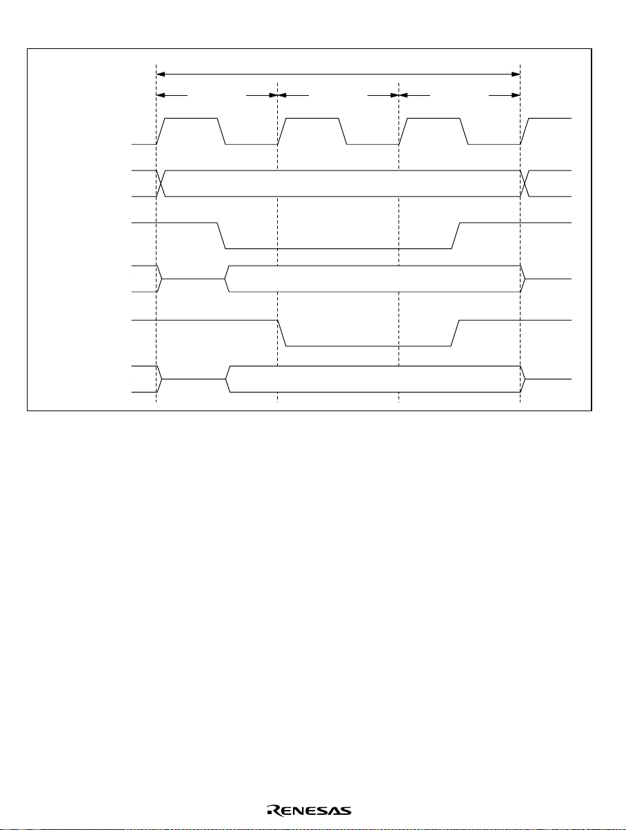
Three-state access to on-chip peripheral modules
Bus cycle
φ or φ
SUB
Internal
address bus
Internal
read signal
Internal
data bus
(read access)
Internal
write signal
Internal
data bus
(write access)
Figure 2.13 On-Chip Peripheral Module Access Cycle (3-State Access)
T1 state
T2 state T3 state
Address
Read data
Write data
Rev. 6.00, 08/04, page 56 of 628
Page 87

2.7 CPU States
2.7.1 Overview
There are four CPU states: the reset state, program execution state, program halt state, and
exception-handling state. The program execution state includes active (high-speed or mediumspeed) mode and subactive mode. In the program halt state there are a sleep (high-speed or
medium-speed) mode, standby mode, watch mode, and sub-sleep mode. These states are shown in
figure 2.14. Figure 2.15 shows the state transitions.
CPU state Reset state
The CPU is initialized
Program
execution state
Program halt state
A state in which some
or all of the chip
functions are stopped
to conserve power
The CPU executes successive program
instructions at high speed,
synchronized by the system clock
The CPU executes successive
program instructions at
reduced speed, synchronized
by the system clock
The CPU executes
successive program
instructions at reduced
speed, synchronized
by the subclock
Active
(high speed) mode
Active
(medium speed) mode
Subactive mode
Sleep (high-speed)
mode
Sleep (medium-speed)
mode
Standby mode
Low-power
modes
Watch mode
Subsleep mode
Exception-
handling state
A transient state in which the CPU changes
the processing flow due to a reset or an interrupt
Note: See section 5, Power-Down Modes, for details on the modes and their transitions.
Figure 2.14 CPU Operation States
Rev. 6.00, 08/04, page 57 of 628
Page 88

Reset state
Reset cleared
Exception-handling state
Reset occurs
Reset
occurs
Program halt state
Reset
occurs
SLEEP instruction executed
Interrupt
source
occurs
Interrupt
source
occurs
Program execution state
Exceptionhandling
complete
Figure 2.15 State Transitions
2.7.2 Program Execution State
In the program execution state the CPU executes program instructions in sequence.
There are three modes in this state, two active modes (high speed and medium speed) and one
subactive mode. Operation is synchronized with the system clock in active mode (high speed and
medium speed), and with the subclock in subactive mode. See section 5, Power-Down Modes for
details on these modes.
2.7.3 Program Halt State
In the program halt state there are five modes: two sleep modes (high speed and medium speed),
standby mode, watch mode, and subsleep mode. See section 5, Power-Down Modes for details on
these modes.
2.7.4 Exception-Handling State
The exception-handling state is a transient state occurring when exception handling is started by a
reset or interrupt and the CPU changes its normal processing flow. In exception handling caused
by an interrupt, SP (R7) is referenced and the PC and CCR values are saved on the stack.
For details on interrupt handling, see sectio n 3. 3, Interrupts.
Rev. 6.00, 08/04, page 58 of 628
Page 89
2.8 Memory Map
2.8.1 Memory Map
The memory map of the H8/38024, H8/38024S, and H8/38124 are shown in figure 2.16(1), that of
the H8/38023, H8/38023S, and H8/38123 in figure 2.16(2), that of the H8/38022, H8/38022S, and
H8/38122 in figure 2.16(3), that of the H8/38021, H8/38021S, and H8/38121 in figure 2.16(4),
and that of the H8/38020, H8/38020S, and H8/38120 in figure 2.16(5).
HD64F38024, HD64F38024R, HD64F38124
H'0000
H'0029
H'002A
H'7000
H'7FFF
H'F020
H'F02B
H'F740
H'F74F
H'F780
H'FB7F
H'FB80
H'FF7F
H'FF80
H'FFFF
(flash memory version)
Interrupt vector area
On-chip ROM
Firmware
for on-chip emulator
Not used
Internal I/O register
Not used
LCD RAM (16 bytes)
Not used
(Workarea for reprogramming
flash memory: 1 Kbyte)
On-chip RAM
(2 Kbytes)
User area
(1 Kbyte)
Internal I/O register
(128 bytes)
1
*
2
*
32 Kbytes
(32768 bytes)
1024 bytes
HD64338024 (mask ROM version)
HD64338024S (mask ROM version)
HD64738024 (PROM version)
H'0000
H'0029
H'002A
H'7FFF
H'F740
H'F74F
H'FB80
H'FF7F
H'FF80
H'FFFF
Interrupt vector area
On-chip ROM
Not used
LCD RAM (16 bytes)
Not used
Internal I/O register
(128 bytes)
32 Kbytes
(32768 bytes)
1024 bytesOn-chip RAM
Notes: 1. Not available to the user if the on-chip emulator is used.
2. Used by the programming control program when programming flash memory. Also, not available to the user
if the on-chip emulator is used.
Figure 2.16(1) H8/38024, H8/38024S, and H8/38124 Memory Map
Rev. 6.00, 08/04, page 59 of 628
Page 90

H'0000
H'0029
H'002A
H'5FFF
H'F740
H'F74F
Interrupt vector area
On-chip ROM
Not used
LCD RAM
(16 bytes)
24 Kbytes
(24576 bytes)
H'FB80
H'FF7F
H'FF80
H'FFFF
Figure 2.16(2) H8/38023, H8/38023S, and H8/38123 Memory Map
Rev. 6.00, 08/04, page 60 of 628
Not used
1024 bytesOn-chip RAM
Internal I/O registers
(128 bytes)
Page 91
H'0000
H'0029
H'002A
H'3FFF
H'F740
H'F74F
Interrupt vector area
On-chip ROM
Not used
LCD RAM
(16 bytes)
16 Kbytes
(16384 bytes)
Not used
H'FB80
1024 bytesOn-chip RAM
H'FF7F
H'FF80
H'FFFF
Internal I/O registers
(128 bytes)
Figure 2.16(3) H8/38022, H8/38022S, and H8/38122 Memory Map
Rev. 6.00, 08/04, page 61 of 628
Page 92

H'0000
H'0029
H'002A
H'2FFF
H'F740
H'F74F
Interrupt vector area
On-chip ROM
Not used
LCD RAM
(16 bytes)
12 Kbytes
(12288 bytes)
H'FD80
H'FF7F
H'FF80
H'FFFF
Figure 2.16(4) H8/38021, H8/38021S, and H8/38121 Memory Map
Rev. 6.00, 08/04, page 62 of 628
Not used
512 bytesOn-chip RAM
Internal I/O registers
(128 bytes)
Page 93

H'0000
H'0029
H'002A
H'1FFF
H'F740
H'F74F
Interrupt vector area
On-chip ROM
Not used
LCD RAM
(16 bytes)
8 Kbytes
(8192 bytes)
Not used
H'FD80
512 bytesOn-chip RAM
H'FF7F
H'FF80
H'FFFF
Internal I/O registers
(128 bytes)
Figure 2.16(5) H8/38020, H8/38020S, and H8/38120 Memory Map
Rev. 6.00, 08/04, page 63 of 628
Page 94

2.9 Application Notes
2.9.1 Notes on Data Access
1. Access to Empty Areas:
The address space of the H8/300L CPU includes empty areas in addition to the RAM,
registers, and ROM areas available to the user. If these empty areas are mistakenly accessed
by an application program, the following results will occur.
Data transfer from CPU to empty area:
The transferred data will be lost. This action may also cause the CPU to misoperate.
Data transfer from empty area to CPU:
Unpredictable data is transferred.
2. Access to Internal I/O Registers:
Internal data transfer to or from on-chip modules other than the ROM and R AM areas makes
use of an 8-bit data width. If word access is attempted to these areas, the following results will
occur.
Word access from CPU to I/O register area:
Upper byte: Will be written to I/O register.
Lower byte: Transferred data will be lost.
Word access from I/O register to CPU:
Upper byte: Will be written to upper part of CPU register.
Lower byte: Unpredictable data will be written to lower part of CPU r e gister.
Byte size instructions should therefore be used when transferring data to or from I/O registers
other than the on-chip ROM and RAM areas. Figure 2.17 shows the data size and number of
states in which on-chip peripheral modules can be accessed.
Rev. 6.00, 08/04, page 64 of 628
Page 95

H'0000
H'0029
H'002A
Interrupt vector area
(42 bytes)
Access
Word Byte
States
32 Kbytes
On-chip ROM
1
*
H'7FFF
Not used
H'F020
H'F02B
H'F740
H'F74F
H'F780
H'FB7F
2
*
H'FB80
H'FF7F
H'FF80
H'FFFF
Notes:
These examples apply to the H8/38024.
1. On the H8/38024, H8/38124, and H8/38024S, 32 Kbytes and the address is H'7FFF; on the
2. On the H8/38021, H8/38121, H8/38021S, H8/38020, H8/38120, and H8/38020S, 512 bytes
3. Only the HD64F38024, HD64F38024R, and HD64F38124 are equipped with internal I/O
Internal I/O registers
Not used
LCD RAM
(16 bytes)
Not used
(1-Kbyte work area for flash
memory programming)
Internal RAM
User Area
Internal I/O registers
(128 bytes)
H8/38023, H8/38123, and H8/38023S, 24 Kbytes and the address is H'5FFF; on the
H8/38022, H8/38122, and H8/38022S, 16 Kbytes and the address is H'3FFF; on the
H8/38021, H8/38121, and H8/38021S, 12 Kbytes and the address is H'2FFF; on the
H8/38020, H8/38120, and H8/38020S, 8 Kbytes and the address is H'1FFF.
and the address is H'FD80.
registers from H'F020 to H'F02B and on-chip RAM from H'F780 to H'FB7F. Attempting to
access these areas on products other than the HD64F38024, HD64F38024R, and
HD64F38124 will result in access to an empty area.
3
*
3
*
1024 bytes
H'FF98 to H'FF9F
H'FFA8 to H'FFAF
×
×
×
×
×
×
2
2
2
2
2
2
3
2
3
2
Figure 2.17 Data Size and Number of States for Access to and from
On-Chip Peripheral Modules
Rev. 6.00, 08/04, page 65 of 628
Page 96

2.9.2 Notes on Bit Manipulation
The BSET, BCLR, BNOT, BST, and BIST instructions read one byte of data, modify the data,
then write the data byte again. Special care is required when using these instructions in cases
where two registers are assigned to the same address, in the case of registers that include writeonly bits, and when the instruction accesses an I/O port.
Order of Operation Operation
1 Read Read byte data at the designated address
2 Modify Modify a designated bit in the read data
3 Write Write the altered byte data to the designated address
1. Bit manipulation in two registers assigned to the same address
Example 1: timer load register and timer counter
Figure 2.18 shows an example in which two timer registers share the same address. When a bit
manipulation instruction accesses the timer load register and timer counter of a reloadable timer,
since these two registers share the same address, the following operations take place.
Order of Operation Operation
1 Read Timer counter data is read (one byte)
2 Modify The CPU modifies (sets or resets) the bit designated in the instruction
3 Write The altered byte data is written to the timer load register
The timer counter is counting, so the value read is not necessarily the same as the value in the
timer load register. As a result, bits other than the intended bit in the timer load register may be
modified to the timer counter value.
Count clock Timer counter
Reload
Timer load register
Read
Write
Internal
data bus
Figure 2.18 Timer Configuration Example
Rev. 6.00, 08/04, page 66 of 628
Page 97

Example 2: BSET instruction executed designating port 3
and P36 are designated as input pins, with a low-level signal input at P37 and a high-level
P3
7
signal at P3
example, the BSET instruction is used to change pin P3
. The remaining pins, P35 to P31, are output pins and output low-level signals. In this
6
to high-level output.
0
[A: Prior to executing BSET]
P3
7
P3
6
P3
5
P3
4
P3
3
P3
2
P3
1
P3
0
Input/output Input Input Output Output Output Output Output Output
Pin state Low level High level Low level Low level Low level Low level Low level Low level
PCR300111111
PDR310000000
[B: BSET instruction executed]
BSET #0 , @PDR3 The BSET instruction is executed designating port 3.
[C: After executing BSET]
P3
7
Input/output Input Input Output Output Output Output Output Output
Pin state Low level High level Low level Low level Low level Low level Low level High level
PCR300111111
PDR3 0 1000001
P3
6
P3
5
P3
4
P3
3
P3
2
P3
1
P3
0
[D: Explanation of how BSET operates]
When the BSET instruction is executed, first the CPU reads port 3.
Since P3
P3
and P36 are input pins, the CPU reads the pin states (low-level and high-level input).
7
to P30 are output pins, so the CPU reads the value in PDR3. In this example PDR3 has a value
5
of H'80, but the value read by the CPU is H'40.
Next, the CPU sets bit 0 of the read data to 1, changing the PDR3 data to H'41. Finally, the CPU
writes this value (H'41) to PDR3, completing execution of BSET.
As a result of this operation, bit 0 in PDR3 becomes 1, and P3
outputs a high-level signal.
0
However, bits 7 and 6 of PDR3 end up with different values.
To avoid this problem, store a copy of the PDR3 data in a work area in memory. Perform the bit
manipulation on the data in the work area, then write this data to PDR3.
Rev. 6.00, 08/04, page 67 of 628
Page 98

[A: Prior to executing BSET]
MOV. B #80, R0L The PDR3 value (H'80) is written to a work area in memory
MOV. B R0L, @RAM0 (RAM0) as well as to PDR3
MOV. B R0L, @PDR3
P3
7
P3
6
P3
5
P3
4
P3
3
P3
2
P3
1
P3
0
Input/output Input Input Output Output Output Output Output Output
Pin state Low level High level Low level Low level Low level Low level Low level Low level
PCR300111111
PDR310000000
RAM010000000
[B: BSET instruction executed]
BSET #0 , @RAM0 The BSET instruction is executed designating the PDR3
work area (RAM0).
Rev. 6.00, 08/04, page 68 of 628
Page 99

2. Bit manipulation in a register containing a write-only bit
Example 3: BCLR instruction executed designating port 3 control register PCR3
As in the examples above, P3
high-level signal at P3
6
signals. In this example, the BCLR instruction is used to change pin P3
and P36 are input pins, with a low-level signal input at P37 and a
7
. The remaining pins, P35 to P30, are output pins that output low-level
to an input port. It is
0
assumed that a high-level signal will be input to this input pin.
[A: Prior to executing BCLR]
P3
7
Input/output Input Input Output Output Output Output Output Output
Pin state Low level High level Low level Low level Low level Low level Low level Low level
PCR300111111
PDR310000000
P3
6
P3
5
P3
4
P3
3
P3
2
P3
1
P3
0
[B: BCLR instruction executed]
BCLR #0 , @PCR3 The BCLR instruction is executed designating PCR3.
[C: After executing BCLR]
P3
7
Input/output Output Output Output Output Output Output Output Input
Pin state Low level High level Low level Low level Low level Low level Low level High level
PCR3 1 1111110
PDR310000000
P3
6
P3
5
P3
4
P3
3
P3
2
P3
1
P3
0
[D: Explanation of how BCLR operates]
When the BCLR instruction is executed, first the CPU reads PCR3. Since PCR3 is a write-only
register, the CPU reads a value of H'FF, even though the PCR3 value is actually H'3F.
Next, the CPU clears bit 0 in the read data to 0, changing the data to H'FE. Finally, this value
(H'FE) is written to PCR3 and BCLR instruction execution ends.
As a result of this operation, bit 0 in PCR3 b ecomes 0, making P3
and 6 in PCR3 change to 1, so that P3
and P36 change from input pins to output pins.
7
an input port. However, bits 7
0
To avoid this problem, store a copy of the PCR3 data in a work area in memory. Perform the bit
manipulation on the data in the work area, then write this data to PCR3.
Rev. 6.00, 08/04, page 69 of 628
Page 100
[A: Prior to executing BCLR]
MOV. B #3F, R0L The PCR3 value (H'3F) is written to a work area in memory
MOV. B R0L, @RAM0 (RAM0) as well as to PCR3.
MOV. B R0L, @PCR3
P3
7
P3
6
P3
5
P3
4
P3
3
P3
2
P3
1
P3
0
Input/output Input Input Output Output Output Output Output Output
Pin state Low level High level Low level Low level Low level Low level Low level Low level
PCR300111111
PDR310000000
RAM000111111
[B: BCLR instruction executed]
BCLR #0 , @RAM0 The BCLR instruction is executed designating the PCR3
work area (RAM0).
[C: After executing BCLR]
MOV. B @RAM0, R0L The work area (RAM0) value is written to PCR3.
MOV. B R0L, @PCR3
P3
7
Input/output Input Input Output Output Output Output Output Output
Pin state Low level High level Low level Low level Low level Low level Low level High level
PCR300111110
PDR310000000
RAM000111110
P3
6
P3
5
P3
4
P3
3
P3
2
P3
1
P3
0
Table 2.12 lists the pairs of registers that share identical addresses. Table 2.13 lists the registers
that contain write-only bits.
Rev. 6.00, 08/04, page 70 of 628
 Loading...