

Page 1
OB1203SD
Integrated Context Engine for Heart Rate and Bl ood Oxygen Saturation measurement with BLE
X0008647 Rev.1.2
Feb.8.21
Page 1
Copyright © 2021
TLSR8258
-BT-EVK
The Integrated Context Engine (ICE) for Biosensing
(see Figure 2) includes:
■
Renesas OB1203 reflective photoplethysmography
(PPG), proximity (PS) and light / color (LS/CS)
sensor
■
Telink’s TLSR8258F512 micro controller with
Bluetooth Low Energy (BLE) radio
■
LiPo’s LP201030 rechargeable Li ion battery , 3.7
V, 40mAh, 10
[1] Light and color sensing function not used in this application.
× 30 × 2 mm
3
.
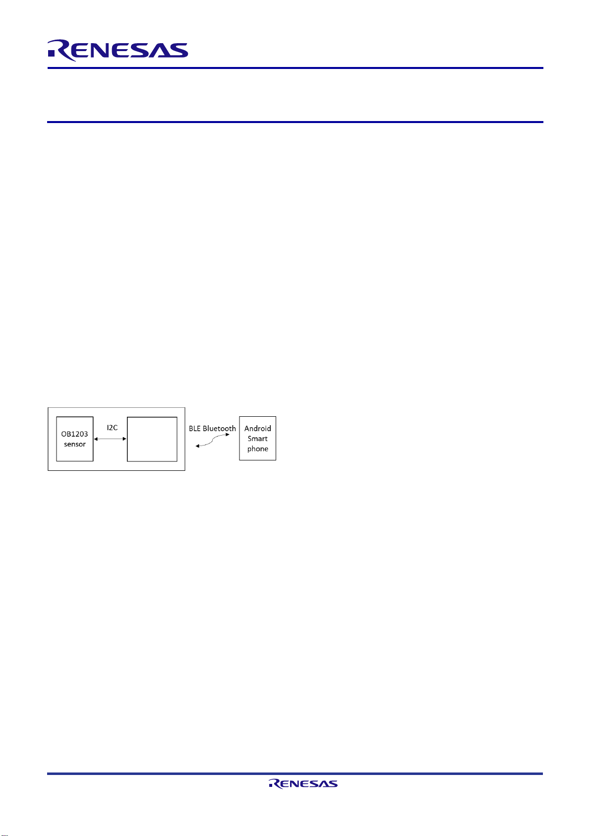
The ICE hardware performs reflective, non-invasive
measurements (e.g., at the fingertip), transmits the data
via BLE to a smartphone or tablet (see Figure 1), where
the Heart Rate (HR) and blood oxygen saturation
(SpO
) are determined by an Android app. During this
2
process the proximity sensor function keeps the
measurement running as long as there is a finger
present.
Controller
Figure 1. Block Diagram of ICE
OB1203 Sensor Features
■
Highly reliable and industry-proven OSIP package
with integrated cover glass for hypoallergenic
products
■
Integrated and factory trimmed LED source, driver,
and photodetector
■
PPG (Heart Rate and Blood Oxygen Concentration):
●
Aesthetic industrial design options with unique
far-red LED allowing SpO
behind visibly dark, IR-transmissive ink.
●
16 to 18 bits output resolution
●
High speed sampling up to 3200 samples per
second for highest resolution and improved
SNR
●
On-chip averaging and FIFO data storage
enable convenient asynchronous access to data
measurements
2
[1]
Evaluation Kit Manual
■
Proximity Sensor:
●
Up to 16 bits resolution
●
Ambient light suppression
●
Analog and digital crosstalk cancelation
■
Wide operation temperature range: -40°C to +85°C
■
Wide supply voltage range:
●
1.7V to 3.6V for digital / analog
●
3.3 V to 5.0 V for LEDs
■
I2C interface capable of 100kHz or 400kHz
communication
■
Programmable level-based interrupt functions
■
Industry’s smallest package: 4.2 × 2 × 1.2 mm3
14-pin module
Radio Mode Features
■
Telink TLSR8258F512
●
BT 4.2 BLE 2.4GHz radio
●
32-bit MCU at 48MHz, 512 kB flash, 32kB SRAM
●
Wide supply voltage range: 1.9V to 3.6V
■
Compact size: 32-pin, 5.0 × 5.0 × 0.75 mm package
ICE Characteristics
■
PCB (see Figure 2):
●
Operation temperature range: -40°C to +85°C
●
PCB supply voltage range: 3.3 V to 6.5V
●
PCB: 40mm × 11mm (21mm with program pads) ×
5mm with USB charge connector (3.1mm without)
●
Program pad PCB section removable
■
Battery life:
●
150 × 30s measurements
●
Typical PCB quiescence current: 0.5 µA at 4V
●
Battery capacity: 40mAh if charged up to 4.2V
●
Battery operation: 3.3V to 4.2V
●
Rechargeable via USB Micro cable
●
> 70% shelf: 1 year stored (-20°C to 30°C)
■
Battery operating temperature range -20C° to + 60°C
Applications
■
Mobile devices: Wearables, Fitness, and Accessories
■
Industrial: Worker Safety, Driver Assist
Page 2

OB1203SD-BT-EVK Evaluation Kit Manual
X0008647 Rev.1.2
Feb.8.21
Page 2
Contents
1. ICE Hardware.................................................................................................................................................. 3
2. Sensor Function............................................................................................................................................. 4
3. Getting Started ............................................................................................................................................... 5
4. Resources ....................................................................................................................................................... 7
4.1 PCB Schematics .................................................................................................................................... 7
4.2 PCB Layout ............................................................................................................................................ 9
4.3 PCB Components ................................................................................................................................ 10
4.4 Programming Pins ............................................................................................................................... 10
4.5 Programming Tools ............................................................................................................................. 10
4.6 Bill of Materials .................................................................................................................................... 11
4.7 OB1203 Run Mode .............................................................................................................................. 11
4.8 HR Algorithm ....................................................................................................................................... 12
4.9 SpO2 Algorithm .................................................................................................................................... 12
4.10 Recharging the Battery ........................................................................................................................ 12
4.11 Troubleshoot ........................................................................................................................................ 12
5. Ordering Information ................................................................................................................................... 13
6. Revision History .......................................................................................................................................... 13
Figures
Figure 1. Block Diagram of ICE ................................................................................................................................ 1
Figure 2. ICE Hardware ............................................................................................................................................ 3
Figure 3. Reflective HR and SpO2 Measurement .................................................................................................... 4
Figure 4. PPG Signal Measured at Finger Tip .......................................................................................................... 4
Figure 5. Recommended Height of a Finger Rest .................................................................................................... 4
Figure 6. PCB Activation Switch ............................................................................................................................... 5
Figure 7. Finger Rest Examples ............................................................................................................................... 6
Figure 8. Components for the OB1203 Sensor ........................................................................................................ 7
Figure 9. OB1203 Schematics .................................................................................................................................. 7
Figure 10. MCU Schematics ..................................................................................................................................... 8
Figure 11. Power Schematics ................................................................................................................................... 8
Figure 12. Connector Schematics ............................................................................................................................ 9
Figure 13. PCB Bottom with Telink Chip Left of the Middle ..................................................................................... 9
Figure 14. PCB Top with OB1203 at the Right ......................................................................................................... 9
Figure 15. PCB Functions ....................................................................................................................................... 10
Figure 16. Functions of Programming Pins ............................................................................................................ 10
Tables
Table 1. Bill of Materials ......................................................................................................................................... 11
Page 3
OB1203SD-BT-EVK Evaluation Kit Manual
X0008647 Rev.1.2
Feb.8.21
Page 3
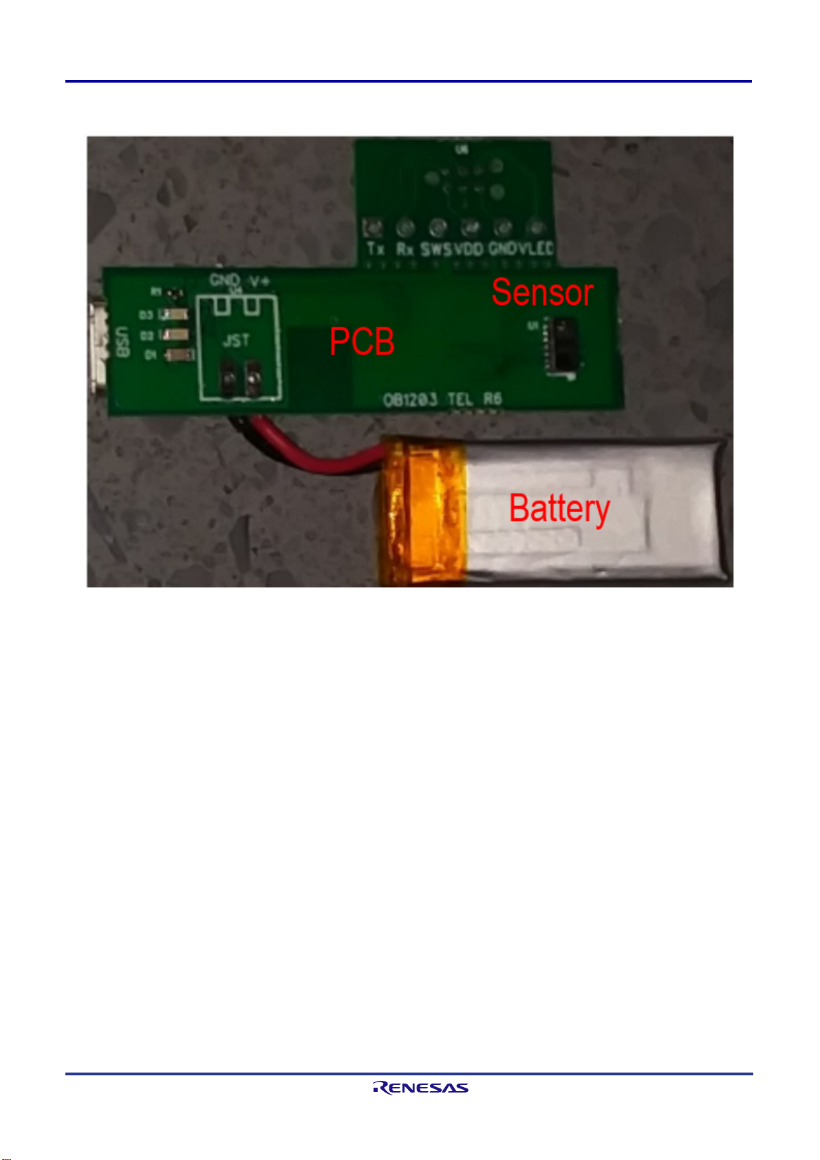
1. ICE Hardware
Figure 2. ICE Hardware
Page 4
OB1203SD-BT-EVK Evaluation Kit Manual
X0008647 Rev.1.2
Feb.8.21
Page 4
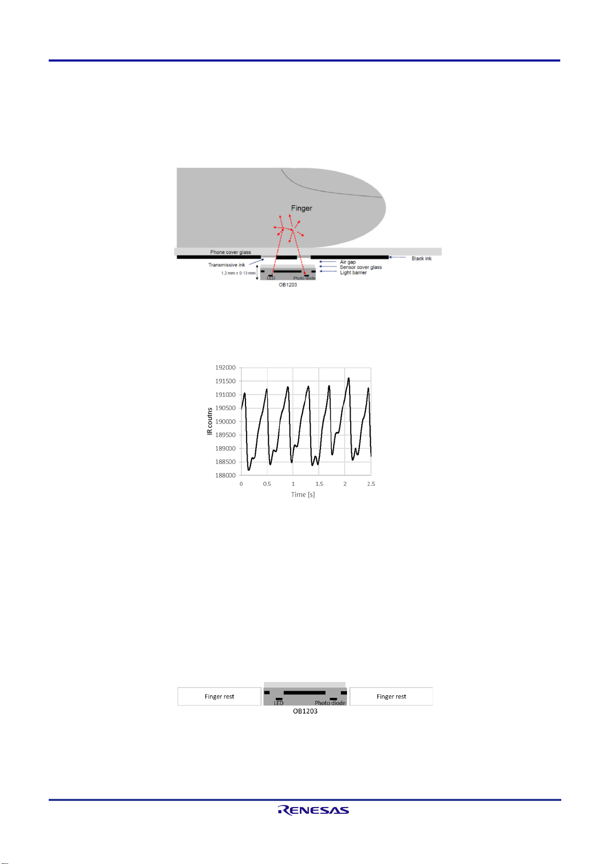
2. Sensor Function
Figure 3 shows the principal of a reflective measu rement. In this case the sensor is located under a cover glass
that uses black and IR transmissive ink to visibly hide the PCB / sensor module. Light from the sensor module’ s
LED is reflected from the finger tissue and detected by the photo diode. As blood absorbs light, changes in bl ood
volume (caused by the heart beat) generate a small change in the intensity of the reflected light.
Figure 3. Reflective HR and SpO2 Measurement
Figure 4 shows this signal change of about 3,000 counts (peak to peak) on top of a DC signal of 190,000 counts
due to direct reflections from the finger tissue.
Figure 4. PPG Signal Measured at Finger Tip
The DC content of the signal as well as light reflections in the sensor set up (like reflections from the cover glass,
etc.) are called optical crosstalk. For a high AC t o DC ratio, a good AC signal and / or a small DC signal are key.
■
In order to get a good blood flow / good AC signal, the finger pressure onto the sensor needs to be light.
■
In order to keep the optical cross talk small, the dist ance from the sensor to the finger should be kept to a
minimum.
For example, without using a cover glass the f inger pressure can be kept low by using a finger rest (like the
cover of the provided sensor house) to spread the finger – sensor force over a larger area.
To recycle some of the diffused light the best col or f or the finger rest is white. To avoid additional optical cros s
talk the finger rest should not be thicker than the package (see Figure 5).
Figure 5. Recommended Height of a Finger Rest
Page 5
OB1203SD-BT-EVK Evaluation Kit Manual
X0008647 Rev.1.2
Feb.8.21
Page 5
3. Getting Started
1. Install the Android app:
a. Download the app from the USB stick or GitHub
(
https://github.com/hyperdga/Android_OB1203_serial_BLE)
b. Click on the app to install.
c. Go to Settings -> Apps -> IDT HR Sensor -> Permissions -> activate ‘your locati on’ .
d. Turn on Bluetooth.
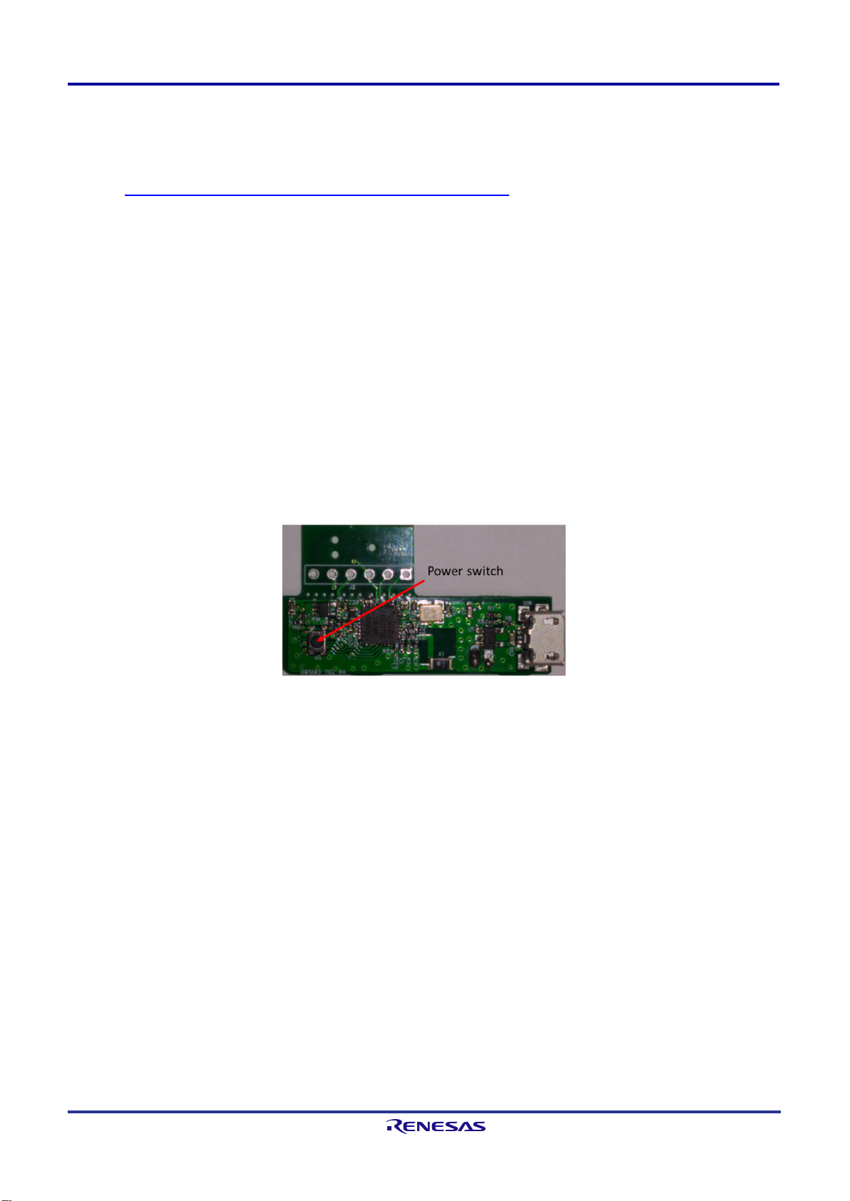
e. Open app. Activate sensor board by pushing the a ct ivation switch (Figure 6). Keep finger off sensor to
get a low data rate while pairing Android device with sen sor. App asks for Bluetooth pairing. After pairing
close app and reopen it.
f. After sensor re-programming unpair and pair again.
g. If Bluetooth does not connect, turn Bluetooth off / on and / or reboot Android device.
2. Open the app.
3. Put your finger on the heart rate sensor. Apply pressure until the activation switch on the bottom side of the
PCB (see arrow in Figure 6) clicks. Keep pressure until counter starts counting.
The pressure level sufficient to activate the switch is not required during measurement, as the sensor boa rd
stays active for about 30 seconds after the switch i s released. Less pressure on the blood vessels produce
better results.
Figure 6. PCB Activation Switch
4. The proximity function of the sensor deactivates / reactivates the red LED and heart rate measurement if the
finger is out of / back in range. This allows to relax or repositioning the finger without losing Bluetooth
connection.
5. When activated, the sensor measures the reflecte d LED light signals and transmits them to the Android
device which calculates and displays heart rate and S pO2.
6. A Finger Rest around the sensor (examples are shown i n F igure 7) distributes the force between sensor and
finger, improving the blood flow and accuracy of measurement.
Page 6

OB1203SD-BT-EVK Evaluation Kit Manual
X0008647 Rev.1.2
Feb.8.21
Page 6
Figure 7. Finger Rest Examples
Page 7

OB1203SD-BT-EVK Evaluation Kit Manual
X0008647 Rev.1.2
Feb.8.21
Page 7
4. Resources
4.1 PCB Schematics
■
The PCB contains the OB1203 and Telink devices a s well as the following components:
●
Voltage stabilization and bypass capacitors for t he OB1203
●
Voltage stabilization and bypass capacitors, ant enna, and quartz for the Telink module
●
Pull-up resistors for the I2C bus and the interrupt
●
A 3.3V voltage regulator
●
A normally open-power switch
●
A re-chargeable battery and a USB 5V to 4.2V Li Ion batt ery charger
Figure 8. Components for the OB1203 Sensor
Figure 9. OB1203 Schematics
Page 8

OB1203SD-BT-EVK Evaluation Kit Manual
X0008647 Rev.1.2
Feb.8.21
Page 8
Figure 10. MCU Schematics
(Note: The battery voltage sense feature is supported by HW but not programmed yet in FW.)
Figure 11. Power Schematics
(Note: When the switch U2 is pressed (upper left), the U12 becomes conductive and the MCU wakes up. The MCU keeps the wake
line high for about 40 seconds leaving U12 conductive. When releasing the wake line, the system pow er is sw itched off.)
Page 9

OB1203SD-BT-EVK Evaluation Kit Manual
X0008647 Rev.1.2
Feb.8.21
Page 9
4.2 PCB Layout
Figure 12. Connector Schematics
Figure 13. PCB Bottom with Telink Chip Left of the Middle
Figure 14. PCB Top with OB1203 at the Right
Page 10

OB1203SD-BT-EVK Evaluation Kit Manual
X0008647 Rev.1.2
Feb.8.21
Page 10
4.3 PCB Components
4.4 Programming Pins
Figure 15. PCB Functions
4.5 Programming Tools
Hardware:
■
Telink Programmer, available from Telink
Software:
■
Telink-Semi IDE
■
Telink BDT
a. Open the .bin file.
b. Select 8258
c. Connect the tool to ICE PCB.
d. Click Erase.
[b]
for C coding and compiling
[b]
(Burn & Debug) for code (.bin file) uploading:
Figure 16. Functions of Programming Pins
(Note: Remove re-chargeable battery for programming)
Page 11

OB1203SD-BT-EVK Evaluation Kit Manual
X0008647 Rev.1.2
Feb.8.21
Page 11
RefDes Value
Name
Manufacturer
A1 2.4GHz AN T3216A 063R2400A Yageo
C1 18pF CAP 0402 ti ght
C2 1.2pF CAP 0402 ti ght
C3 220pF CAP 0402 ti ght
C4 1.8pF CAP 0402 ti ght
C5 1pF CAP 0402 ti ght
C6, C10, C11, C17 0.1uF CAP 0402 ti ght
C7 4.7uF CAP_0603
C8, C9 10uF CA P_0603
C12, C13 15pF CAP 0402 ti ght
C14, C19, C20, C21 1uF CAP 0402 ti ght
C15 22uF CAP_0603
C16 0.2uF CAP 0402 ti ght
C18
2.2uF CAP 0402 ti ght
C22 DNP
CAP 0402 ti ght
D1 SML-D12U1WT86 LED Red 0603 Rohm
D2, D3 SML-E12M8WT86 Rohm LED Green 0603 Rohm
J2 HDR- 1x 6
L1 1.3nH 0402 IN D
L2 3.3nH 0402 IN D
L4
10uH IN D_0603
R1 200 RES 0402 ti ght
R2
2M RES 0402 tight
R3 10M RES 0402 ti ght
R4, R9 1M RES 0402 ti ght
R5, R10 3.9M
RES 0402 ti ght
R6 15k RES 0402 ti ght
R7, R8 100 RES 0402 ti ght
R11
3.3M RES 0402 tigh t
U1 OB1203
U2 PTS 830GX140 swi tch C&K
U3 ECS-240-12-33Q-JES- TR?
U4 JST+pad 2 pin batt
U5 TLSR8258F512ET32 Telink
U6 Tag_connect_6_ARM
U8 TLV 70033DCKR
U9 TS881I CT
U10 USB m i cro AMP 10118192- 0002LF
U11 500mA Li Po charger MCP 73831T- 2A TI /OT
U12 PMZ950UPEYL l ow l eakage PMOS Nexperia
e. Click Activate.
f. Click Download.
g. Click Start mcu.
[b]
Available with user manual from https://www.telink-semi.com/.
4.6 Bill of Materials
4.7 OB1203 Run Mode
■
1600 samples per second
■
16 times averaging on OB1203 before data gets stored in FIFO
■
Automatic Gain control adjusting the LED currents to keep signal between 70 and 100 % of ADC count range
Table 1. Bill of Materials
Page 12

OB1203SD-BT-EVK Evaluation Kit Manual
X0008647 Rev.1.2
Feb.8.21
Page 12
4.8 HR Algorithm
■
Partial autocorrelation coarse / fine search method
4.9 SpO2 Algorithm
■
Collect about 2.5s worth of data
■
Measure and remove DC
■
Remove slope
■
Measure RMS
■
R = (Red_rms/Red_dc) / (IR_rm s/IR_dc)
■
SpO2 = f(R), where f is a polynomial fit to hypoxia
■
Calibration data
4.10 Recharging the Battery
■
Use a male micro USB to male USB A cable
■
Charge time around 90min
■
Do not operate the module and keep sensor face clear from objects during charging
4.11 Troubleshoot
Android app starts but shows no data.
1. Tip on the commands in upper window line:
a. Restart Bluetooth device scan.
b. Restart Bluetooth connection.
2. Check phone settings, network, Bluetooth, and pair with OB1203.
a. Bluetooth pairing shows error message ‘Pairing rejected by OB_1203’. OB1203 was already Bluetooth
connected.
b. Un-pair Bluetooth and pair again. Reboot the phone.
Page 13

OB1203SD-BT-EVK Evaluation Kit Manual
X0008647 Rev.1.2
Feb.8.21
Page 13
Orderable Part Number
Description
OB1203SD-BT-EVK
OB1203SD-BT Evaluation Board
Revision
Date
Description
1.2
Feb.8.21
Changed to PCB version R6.
1.1
May.4.20
Reformatted headers and footers within document.
1.0
Jan.10.19
Initial release.
5. Ordering Information
6. Revision History
Updated the document to the latest template.
Redefined document title.
Page 14

IMPORTANT NOTICE AND DISCLAIMER
RENESAS ELECTRONICS CORPORATION AND ITS SUBSIDIARIES (“RENESAS”) PROVIDES TECHNICAL
SPECIFICATIONS AND RELIABILITY DATA (INCLUDING DATASHEETS), DESIGN RESOURCES (INCLUDING
REFERENCE DESIGNS), APPLICATION OR OTHER DESIGN ADVICE, WEB TOOLS, SAFETY INFORMATION, AND
OTHER RESOURCES “AS IS” AND WITH ALL FAULTS, AND DISCL AIMS ALL WARRANTIES, EXPRESS OR IMPLIED,
INCLUDING, WITHOUT LIMITATION, ANY IMPLIED WARRANTIES OF MERCHANTABILITY, FITNESS FOR A
PARTICULAR PURPOSE, OR NON-INFRINGEMENT OF THIRD PARTY INTELLECTUAL PROPERTY RIGHTS.
These resources are intended for developers skilled in the art designing with Renesas products. You are solely responsible
for (1) selecting the appropriate products for your application, (2) designing, validating, and testing your application, and (3)
ensuring your application meets applicable standards, and any other safety, security, or other requirements. These
resources are subject to change without notice. Renesas grants you permission to use these resources only for
development of an application that uses Renesas products. Other reproduction or use of these resources is strictly
prohibited. No license is granted to any other Renesas intellectual property or to any third party intellectual property.
Renesas disclaims responsibility for, and you will fully indemnify Renesas and its representatives against, any claims,
damages, costs, losses , or liabilities arising out of your use of these resources. Renesas' products are provided only subject
to Renesas' Terms and Conditions of Sale or other applicable terms agreed to in writing. No use of any Renesas resources
expands or otherwise alters any applicable warranties or warranty disclaimers for these products.
Corporate Headquarters
TOYOSU FORESIA, 3-2-24 Toyosu,
Koto-ku, Tokyo 135-0061, Japan
www.renesas .com
Trademarks
Renesas and the Renesas logo are trademarks of Renesas
Electronics Corporation. All trad emarks and registered
trademarks are the property of their respective owners.
(Rev.1.0 Mar 2020)
Contact Information
For further information on a product, technology, the most
up-to-date version of a document, or your nearest sales
office, please visit:
www.renesas .com/contact/
© 2020 Renesas Electronics Corporation. All rights reserved.
 Loading...